WO2012144403A1 - Appareil et procédé pour la cristallisation d'un film amorphe - Google Patents
Appareil et procédé pour la cristallisation d'un film amorphe Download PDFInfo
- Publication number
- WO2012144403A1 WO2012144403A1 PCT/JP2012/059978 JP2012059978W WO2012144403A1 WO 2012144403 A1 WO2012144403 A1 WO 2012144403A1 JP 2012059978 W JP2012059978 W JP 2012059978W WO 2012144403 A1 WO2012144403 A1 WO 2012144403A1
- Authority
- WO
- WIPO (PCT)
- Prior art keywords
- laser light
- laser beam
- amorphous film
- region
- objective lens
- Prior art date
- Legal status (The legal status is an assumption and is not a legal conclusion. Google has not performed a legal analysis and makes no representation as to the accuracy of the status listed.)
- Ceased
Links
Images

Classifications
-
- H—ELECTRICITY
- H10—SEMICONDUCTOR DEVICES; ELECTRIC SOLID-STATE DEVICES NOT OTHERWISE PROVIDED FOR
- H10P—GENERIC PROCESSES OR APPARATUS FOR THE MANUFACTURE OR TREATMENT OF DEVICES COVERED BY CLASS H10
- H10P34/00—Irradiation with electromagnetic or particle radiation of wafers, substrates or parts of devices
- H10P34/40—Irradiation with electromagnetic or particle radiation of wafers, substrates or parts of devices with high-energy radiation
- H10P34/42—Irradiation with electromagnetic or particle radiation of wafers, substrates or parts of devices with high-energy radiation with electromagnetic radiation, e.g. laser annealing
-
- H—ELECTRICITY
- H10—SEMICONDUCTOR DEVICES; ELECTRIC SOLID-STATE DEVICES NOT OTHERWISE PROVIDED FOR
- H10P—GENERIC PROCESSES OR APPARATUS FOR THE MANUFACTURE OR TREATMENT OF DEVICES COVERED BY CLASS H10
- H10P14/00—Formation of materials, e.g. in the shape of layers or pillars
- H10P14/20—Formation of materials, e.g. in the shape of layers or pillars of semiconductor materials
- H10P14/34—Deposited materials, e.g. layers
- H10P14/3402—Deposited materials, e.g. layers characterised by the chemical composition
- H10P14/3404—Deposited materials, e.g. layers characterised by the chemical composition being Group IVA materials
- H10P14/3411—Silicon, silicon germanium or germanium
-
- H—ELECTRICITY
- H10—SEMICONDUCTOR DEVICES; ELECTRIC SOLID-STATE DEVICES NOT OTHERWISE PROVIDED FOR
- H10P—GENERIC PROCESSES OR APPARATUS FOR THE MANUFACTURE OR TREATMENT OF DEVICES COVERED BY CLASS H10
- H10P14/00—Formation of materials, e.g. in the shape of layers or pillars
- H10P14/20—Formation of materials, e.g. in the shape of layers or pillars of semiconductor materials
- H10P14/38—Formation of materials, e.g. in the shape of layers or pillars of semiconductor materials characterised by treatments done after the formation of the materials
- H10P14/3802—Crystallisation or recrystallisation of non-monocrystalline semiconductor materials, e.g. regrowth
- H10P14/3808—Crystallisation or recrystallisation of non-monocrystalline semiconductor materials, e.g. regrowth using laser beams
Definitions
- the present invention relates to an amorphous film crystallization apparatus for sequentially performing side surface crystallization by irradiating a laser beam to an amorphous film, and a method therefor.
- Patent Document 1 propose SLS (sequential ⁇ ⁇ lateral solidification) technology for producing huge single crystal silicon by inducing lateral growth of silicon crystal using an energy source as a laser. ing.
- the SLS technology is based on the phenomenon that silicon grains grow in a direction perpendicular to the boundary surface between liquid silicon and solid phase silicon.
- the silicon grain is laterally grown to a predetermined length to crystallize the amorphous silicon thin film.
- Patent Document 3 it is proposed in Patent Document 3 to provide a method with improved production efficiency when sequentially using a lateral crystallization (SLS) method to crystallize silicon.
- the optical member used in the conventional apparatus is composed of the laser light transmission region and the laser light shielding region.
- the laser light shielding region completely shields the laser beam, so that the pattern of the laser light transmission region can be accurately projected as an image on the amorphous film as the irradiation object.
- the laser light shielding region is composed of a metal such as Cr or CrO film attached to quartz glass, etc., and absorbs the incident laser light and converts the light into heat to shield the laser light. Therefore, there is a problem that high-temperature heat is generated and the Cr film or the CrO film is damaged. Further, when heat is generated in the optical member, air convection is generated, which causes distortion of the pattern image by the optical member.
- a method of cooling the optical member is also conceivable in order to prevent the above-described adverse effects caused by the generation of heat. For example, it is conceivable to cool the optical member by blowing air, but turbulence may occur in the air that has cooled the optical member, which may cause distortion of the pattern image. Although a method using a coolant such as water is conceivable, there is a problem that it is difficult to control the flow rate of the coolant or to control the vapor by evaporation of the coolant.
- the present invention has been made to solve the above-described problems of the prior art, and reduces the generation of heat in the optical member during laser light irradiation without taking a cooling means, thereby preventing adverse effects due to temperature rise.
- An object is to provide an amorphous film crystallization apparatus and a crystallization method that can be eliminated.
- the first present invention is A laser light source that outputs laser light to irradiate the amorphous film;
- a laser light transmission region that is disposed on the laser beam path of the optical system on the front side of the objective lens and transmits a part of the laser beam, and a laser beam shielding area that blocks a part of the laser beam
- an optical member that forms an image pattern by the laser light transmitting region and the laser light shielding region,
- the optical member is smaller than a value (R / M) obtained by a product of a resolution (R) of the objective lens and a reciprocal of a magnification (M) of the objective lens in the laser light shielding region, and the laser light.
- the laser beam transmission part for temperature rise suppression which has the control dimension larger than the wavelength of the above, and enables transmission of the laser beam is provided.
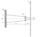
- the magnification (M) of the objective lens is the ratio (b / a) between the distance (b) between the amorphous film and the objective lens and the distance (a) between the optical member and the objective lens, or on the amorphous film. It is determined by the ratio (d / D) of the pattern image size (d) and the pattern image size (D) of the optical member.
- the amorphous film crystallization apparatus is the amorphous film crystallization apparatus according to the first aspect, wherein the laser beam transmission part for suppressing temperature rise has a narrow width on the laser beam irradiation surface. It has a shape.
- the temperature rise suppression laser light transmitting portion is a circle having a diameter of the restriction dimension on the laser light irradiation surface. It has a shape.
- the amorphous film crystallization apparatus according to any one of the first to third aspects of the present invention, wherein the laser beam transmitting part for suppressing temperature rise has a through-site or a relative transmittance of the laser beam. It is characterized by comprising a high part.
- the optical member in any one of the first to fourth aspects of the present invention, has an unirradiated region where the laser beam is not irradiated.
- An amorphous film crystallization apparatus is characterized in that, in any of the first to fifth aspects of the present invention, the amorphous film is sequentially subjected to side surface crystallization by irradiation with the laser beam. To do.
- a laser beam is irradiated through an optical member having a laser beam transmission region and a laser beam shielding region, and the optical is controlled according to the laser beam transmission region and the laser beam shielding region.
- a crystallization method of condensing a laser beam of a pattern transmitted through a member with an objective lens and irradiating the amorphous film, and sequentially crystallizing the amorphous film by side crystallization A part of the laser light irradiated to the laser light shielding area is made smaller than the product of the resolution of the objective lens and the reciprocal of the magnification in the laser light shielding area to pass through the optical member, and at least A part of the irradiation is performed to the irradiation region where the amorphous film is irradiated with the laser beam transmitted through the laser beam transmission region.
- the laser light applied to the laser beam transmission part for suppressing temperature increase in the laser beam shielding area is transmitted through the region of the laser beam transmission part for suppressing temperature increase in the laser beam shielding area.
- it does not irradiate with sufficient energy on the amorphous film by passing through a region having a regulation dimension smaller than the product of the resolution of the objective lens and the reciprocal of the magnification.
- the resolution of the objective lens is the minimum dimension that allows the pattern of the optical member to be patterned on the amorphous film by laser light irradiation.
- magnification (M) of the objective lens can be determined as follows.
- the distance between the objective lens and the optical member is the distance between the optical center of the objective lens on the optical axis and the surface of the optical member.
- the distance between the objective lens and the amorphous film is the optical center of the objective lens on the optical axis and the surface of the amorphous film. It can be shown by the distance.
- the region of the laser beam transmitting portion for suppressing temperature increase does not have a size smaller than the product of the resolution of the objective lens and the reciprocal of the magnification, the laser beam transmitted through the region has sufficient energy. In this state, the amorphous film is irradiated to impair the function as a laser light shielding region.
- the temperature rise suppression laser beam transmitting portion has a regulation size smaller than the product in any direction (in the plane direction) at any position of the temperature increase suppression laser beam transmission portion in the plane direction. It has a dimension smaller than the product.
- the regulation dimension of the laser beam transmitting part for suppressing temperature rise does not have a dimension larger than the wavelength of the laser beam, diffraction is conspicuous when the laser beam is transmitted through the laser beam transmitting part for temperature increase suppression. And is scattered outside the irradiated surface of the amorphous film. For this reason, it is necessary for the laser beam transmission part for temperature rise suppression to have a regulation dimension larger than the wavelength of the laser beam.
- the fact that the laser beam transmitting part for suppressing temperature increase has a regulation dimension larger than the wavelength of the laser beam indicates that the regulation dimension satisfies this condition.
- the regulation size required for the laser beam transmission part for suppressing the temperature increase is not limited to a specific numerical value.
- the required regulation dimension is exemplified by a dimension of 0.5 to 1.0 ⁇ m on the amorphous film.
- the optical member in the present invention is not limited to a specific material, and any optical member can be used as long as a laser light irradiation region and a laser light shielding region can be obtained. It can also be formed by film formation or the like.
- the laser beam transmitting region may be any region that can impart energy to the amorphous film to such an extent that the laser beam is transmitted and the side surface crystallization is sequentially performed by irradiating the amorphous film with the laser beam.
- the laser light transmission region may be formed by a penetrating portion, or may be configured by a portion having a relatively high transmittance.
- the laser light shielding region may be a region where the laser light is transmitted with relatively lower energy than the laser light transmitting region, in addition to the region where the laser light is not transmitted. In other words, it is only necessary that the energy of the laser light that passes through the laser light shielding region is distinguished from the energy of the laser light that passes through the laser light transmitting region, and the side crystallization is performed sequentially.
- the laser beam transmission part for temperature rise suppression allows the laser beam to be partially transmitted in the laser beam shielding region when the laser beam is not transmitted in the laser beam shielding region.
- the transmission of the laser light only gives small energy to the amorphous film as compared with the laser light transmission region.
- the laser light transmitting portion for temperature rise suppression transmits the laser light with a higher transmittance than the laser light shielding region.
- the amount of energy given to the amorphous film of the transmitted laser beam in the laser beam transmitting portion for suppressing temperature rise is much smaller than that of the laser beam transmitted through the laser beam transmitting region, so that the side crystallization is not hindered sequentially.
- the shape of the laser beam transmission part for temperature rise suppression is not particularly limited as long as it satisfies the above-mentioned regulation dimension.
- a strip shape having the prescribed regulation dimension in the short width direction can be used.
- the laser beam transmitting portion for suppressing temperature increase is formed of a penetrating portion, it can be said to be a slit shape.
- a plurality of the strips can be arranged in parallel at a predetermined interval, or arranged vertically and horizontally, and the temperature rise of the optical member can be effectively suppressed.
- the shape of the laser beam transmitting portion for suppressing temperature increase can be a circular shape having the above-mentioned regulated size as a diameter.
- the laser beam transmitting portion for suppressing the temperature increase is constituted by a penetrating portion, it can be said to be a hole shape. By increasing the number of the circular shapes, the temperature of the optical member can be effectively suppressed.
- the laser beam transmitting portion for suppressing the temperature increase may be provided on the optical member with a different shape.
- the present invention can be suitably used as an SLS crystallization method and apparatus for manufacturing a polycrystalline or single crystal semiconductor film of a thin film transistor used in a pixel switch or a drive circuit of a liquid crystal display or an organic EL display.
- the laser beam is transmitted through the laser beam transmitting portion for suppressing temperature increase provided in the laser beam shielding region of the optical member so that there is no hindrance to crystallization. Suppresses the generation of heat, effectively prevents damage due to temperature rise, and improves durability. Moreover, generation
- FIG. 1 is a schematic view showing a laser annealing apparatus 1 corresponding to the amorphous film crystallization apparatus of the present invention.
- the laser annealing apparatus 1 has a stage 3 on which a substrate 2 on which an amorphous silicon film is formed is placed. Further, an X movement motor 4a that moves the stage 3 in the X axis direction and a Y movement motor 4b that can move in the Y axis direction are provided.
- An X movement driver 5a and a Y movement driver 5b are electrically connected to each motor. It is connected to the.
- Each driver is connected to a system controller 6 constituted by a computer, and can control each moving motor.
- the laser annealing apparatus 1 includes a laser light source 10 that outputs a laser beam 10a having a predetermined wavelength.
- the silicon film is in an amorphous state before processing.
- a laser light source 10 for example, a laser oscillator LS2000 (1) or LSX315 (wavelength 308 nm, repetition frequency 300 Hz) manufactured by Coherent Co., Ltd. can be used.
- the laser light source 10 is not limited to a specific one in the present invention.
- An attenuator 11 is disposed in the irradiation direction of the laser light 10 a oscillated by the laser light source 10, and an optical system 15 including a mirror 12, a beam shaper 13, an objective lens 14 and the like is disposed in the emission direction of the attenuator 11.
- Laser light 10 a is guided through the optical system 15 and is irradiated onto the silicon film of the substrate 2.
- the attenuator 11 attenuates the laser beam 10a and adjusts it to a predetermined energy.
- a variable attenuator capable of adjusting the attenuation rate can be used.
- the attenuator 11 adjusts the attenuation factor of the laser beam 10a so as for example of about 600 mJ / cm 2 energy density of -1000mJ / cm 2 on the silicon film.
- the mirror 12 deflects the irradiation direction of the laser light 10a output from the laser light source 10.
- the laser light 10a output in the horizontal direction from the laser light source 10 is applied to the substrate 2 on which the silicon film is formed. Therefore, the direction is changed vertically.
- the beam shaper 13 shapes the laser beam 10a into a beam cross-sectional shape such as a rectangular shape or a circular shape.
- the objective lens 14 condenses the laser beam 10a and irradiates the vicinity of the silicon film surface on the substrate 2.
- the distance between the optical center of the objective lens 14 and the silicon film surface on the optical axis is b in the figure. It is shown.
- the silicon film is an object of processing.
- the present invention processes an amorphous film into a crystal film or a crystal film, and the material is limited to silicon. It is not something.
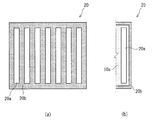
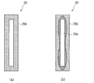
- the optical member 20 has a rectangular shape, and in the surface direction, the strip-shaped laser light transmission region 20a is arranged in parallel so that the long sides are adjacent to each other.
- the adjacent laser light transmission regions 20a are provided at a small interval.
- the optical member 20 is a laser light shielding region 20b in the plane direction except for the laser light transmitting region 20a.
- the manufacturing method of the optical member 20 having the laser light transmission region 20a and the laser light shielding region 20b is not particularly limited as the present invention.
- an optical member is composed of a material that transmits laser light, and a metal thin film is coated by vapor deposition or the like on a region other than the laser light transmitting region 20a using a shadow mask that covers a portion of the laser light transmitting region 20a.
- the light shielding region 20b can be formed.
- the optical member 20 may be obtained by removing the metal thin film by etching or the like in a region corresponding to the laser light transmitting region 20a with respect to the metal thin film coated on the surface of the optical member.
- the optical member 20 body is made of a material that transmits laser light, and a metal film made of Cr or CrO is formed on the laser light shielding region 20b excluding the laser light transmitting region 20a.
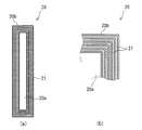
- a narrow laser beam transmitting part 21 for suppressing temperature rise is arranged at intervals along the edge of the laser beam transmitting region 20a. Are in parallel.
- the width of the laser beam transmitting portion 21 for suppressing temperature increase and the interval width between the laser beam transmitting portions 21 for suppressing temperature increase are substantially the same width. Accordingly, in the laser light shielding region 20b, the total area of the laser beam transmitting portion 21 for suppressing the temperature increase and the other total area are about 1 ⁇ 2 each.
- the width of the laser beam transmitting portion 21 for suppressing the temperature increase is smaller than the product (R / M) of the resolution (R) of the objective lens and the inverse of the magnification (M) of the objective lens described below. Furthermore, the width of the laser beam transmitting portion 21 for suppressing temperature increase is larger than the wavelength of the laser beam 10a. In this embodiment, the width exceeds, for example, 308 nm, which is the wavelength of the laser beam 10a. As shown in FIG. 4, the magnification of the objective lens is the ratio (b / a) between the distance (b) between the amorphous film on the substrate 2 and the objective lens 14 and the distance (a) between the optical member 20 and the objective lens 14.
- Laser light 10a is output from the laser light source 10.
- excimer laser light having a wavelength of 308 nm is output.
- the laser light 10 a is adjusted to energy suitable for silicon crystallization by the attenuator 11, deflected by the mirror 12, and enters the beam shaper 13.
- the beam shaper 13 forms the desired beam cross-sectional shape. For example, it is shaped into a beam cross-sectional shape having a major axis of 125 mm and a minor axis of 6 mm.
- the laser beam 10 a that has passed through the beam shaper 13 reaches the optical member 20, is patterned by a pattern according to the shape and arrangement of the laser beam transmission region 20 a, and reaches the objective lens 14.
- the laser beam 10a is condensed when passing through the objective lens 14, and is irradiated on the silicon film on the substrate 2 in a predetermined pattern image.
- Side crystallization can be performed sequentially by changing the position of the optical member 20 and irradiating the silicon film on the substrate 2 with a laser beam 10a in a predetermined pattern image. Further, the relative position between the laser beam 10a and the silicon film can be changed by moving the stage 2 while feeding the pitch by the X moving motor 4a and the Y moving motor 4b.
- the shutter is for blocking the laser beam at the end surface of the substrate not coated with a silicon (amorphous silicon) film.
- the reason why the shutter is arranged after the objective lens 14 is as follows. Depending on whether or not the laser beam 10a passes through the objective lens 14, a temperature change occurs and is affected by a focus shift of the objective lens 14 and the like. Even when the shutter is closed, the influence can be reduced by passing the laser beam 10a through the objective lens 14.
- the shutter is provided with a mirror tilted at 45 °, so that the energy of the laser beam 10a can be consumed toward a beam dump (not shown) without being reflected by the optical system.
- FIG. 2B is a view showing the periphery of the laser light transmission region 20a irradiated with the laser light 10a, and shows a part of the optical member 20.
- the laser beam 10a cannot enter the optical member 20 with a size suitable for the laser beam transmission region 20a due to the vibration of the apparatus and the fluctuation of the position of the laser beam 10a. Therefore, the laser beam 10a is shaped to be larger than the pattern size and is incident on the optical member 20, so that the laser beam 10a is not only irradiated to the laser beam shielding region 20b between the laser beam transmitting regions 20a but also the laser beam transmitting region. Laser light 10a is also irradiated around 20a, and high temperature is generated.
- the region that is not irradiated with laser light is also a non-irradiated region.
- a part of the laser light shielding region 20b around the laser light transmitting region 20a becomes particularly high temperature, and damage is likely to occur over time. Further, even before the damage occurs, air convection occurs, and the pattern image by the optical member 20 is damaged.
- the optical member 20 of this embodiment half the area of the original laser light shielding region 20b is the laser light transmitting portion 21 for suppressing the temperature rise, and this portion is irradiated with the laser light 10a. Heating during heating is suppressed. Thereby, the temperature rise of the whole optical member 20 becomes small.
- the generation of heat can be suppressed by minimizing the metal portion of the laser light shielding region 20b of the optical member 20, damage to the optical member 20 is reduced. can do. Furthermore, the pattern of the optical member 20 can be accurately projected onto the amorphous silicon film.
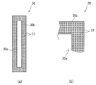
- FIG. 5 shows an optical member 30 of another form, and the optical member 30 has a laser light transmission region 30a and a laser light shielding region 30b as in the above embodiment.
- the optical member 30 instead of the laser beam transmission part 21 for suppressing temperature increase, circular laser beam transmission parts 31 for suppressing temperature increase are scattered in the laser beam shielding region 30b.
- the diameter of the transmission part 31 is smaller than the resolution of the objective lens 14 and larger than the wavelength of the laser beam 10a.
- the total area of the remaining portions of the laser beam transmitting portion 30a for suppressing temperature increase and the laser beam shielding region 30b is substantially the same. Also in this embodiment, when the laser beam 10a is irradiated, the generation of heat in the laser beam shielding region 30b is suppressed, and the occurrence of damage or distortion of the pattern image due to the temperature rise of the optical member 30 is prevented.
Landscapes
- Recrystallisation Techniques (AREA)
Abstract
Le but de la présente invention est de supprimer le chauffage et l'augmentation de température d'un élément optique pour obtenir une lumière laser avec une image d'un motif lors d'une solidification latérale séquentielle. L'invention concerne spécifiquement un appareil qui comprend : une source de lumière laser (10) qui émet une lumière laser (10a) avec laquelle un film amorphe est irradié ; un système optique (15) qui guide la lumière laser jusqu'au film amorphe ; une lentille d'objectif (14) constituant une partie du système optique (15) et collectant la lumière laser avec lequel le film amorphe est irradié ; et un élément optique (20) disposé avant la lentille d'objectif (14) sur le chemin optique de la lumière laser du système optique (15), et comprenant une région transmettant la lumière laser et une région bloquant la lumière laser. L'élément optique (20) comprend, dans la région bloquant la lumière laser, une partie transmettant la lumière laser empêchant l'augmentation de la température avec une taille de régulation plus petite que la valeur du produit de la résolution par l'inverse du grossissement de la lentille d'objectif (14) et plus grande que la longueur d'onde de la lumière laser (10a), ce qui permet la transmission de la lumière laser (10). L'invention concerne également un procédé dans lequel une source de lumière laser (10) émet une lumière laser (10a) avec laquelle un film amorphe est irradié. Un système optique (15) guide la lumière laser jusqu'au film amorphe. Une lentille d'objectif (14) constituant une partie du système optique (15) collecte la lumière laser avec laquelle le film amorphe est irradié. Un élément optique (20) est disposé avant la lentille d'objectif (14) sur le chemin optique de la lumière laser du système optique (15), et comprend une région transmettant la lumière laser et une région bloquant la lumière laser. L'élément optique (20) comprend, dans la région bloquant la lumière laser, une partie transmettant la lumière laser empêchant l'augmentation de la température permettant la transmission de la lumière laser (10) en ayant une taille de régulation plus petite que la valeur du produit de la résolution par l'inverse du grossissement de la lentille d'objectif (14) et plus grande que la longueur d'onde de la lumière laser (10a).
Applications Claiming Priority (2)
| Application Number | Priority Date | Filing Date | Title |
|---|---|---|---|
| JP2011-093994 | 2011-04-20 | ||
| JP2011093994A JP5435590B2 (ja) | 2011-04-20 | 2011-04-20 | アモルファス膜結晶化装置およびその方法 |
Publications (1)
| Publication Number | Publication Date |
|---|---|
| WO2012144403A1 true WO2012144403A1 (fr) | 2012-10-26 |
Family
ID=47041513
Family Applications (1)
| Application Number | Title | Priority Date | Filing Date |
|---|---|---|---|
| PCT/JP2012/059978 Ceased WO2012144403A1 (fr) | 2011-04-20 | 2012-04-12 | Appareil et procédé pour la cristallisation d'un film amorphe |
Country Status (3)
| Country | Link |
|---|---|
| JP (1) | JP5435590B2 (fr) |
| TW (1) | TW201248699A (fr) |
| WO (1) | WO2012144403A1 (fr) |
Cited By (1)
| Publication number | Priority date | Publication date | Assignee | Title |
|---|---|---|---|---|
| WO2018155455A1 (fr) * | 2017-02-21 | 2018-08-30 | 株式会社ブイ・テクノロジー | Dispositif d'irradiation laser, procédé de fabrication de transistor à couches minces, programme et masque de projection |
Families Citing this family (1)
| Publication number | Priority date | Publication date | Assignee | Title |
|---|---|---|---|---|
| JP2019129231A (ja) * | 2018-01-24 | 2019-08-01 | 株式会社ブイ・テクノロジー | レーザ照射装置、投影マスク及びレーザ照射方法 |
Citations (2)
| Publication number | Priority date | Publication date | Assignee | Title |
|---|---|---|---|---|
| JP2004349269A (ja) * | 2003-01-15 | 2004-12-09 | Sharp Corp | 結晶化半導体薄膜の製造方法ならびにその製造装置 |
| JP2005347380A (ja) * | 2004-06-01 | 2005-12-15 | Sharp Corp | 半導体薄膜の製造方法および製造装置 |
-
2011
- 2011-04-20 JP JP2011093994A patent/JP5435590B2/ja not_active Expired - Fee Related
-
2012
- 2012-04-12 WO PCT/JP2012/059978 patent/WO2012144403A1/fr not_active Ceased
- 2012-04-18 TW TW101113815A patent/TW201248699A/zh unknown
Patent Citations (2)
| Publication number | Priority date | Publication date | Assignee | Title |
|---|---|---|---|---|
| JP2004349269A (ja) * | 2003-01-15 | 2004-12-09 | Sharp Corp | 結晶化半導体薄膜の製造方法ならびにその製造装置 |
| JP2005347380A (ja) * | 2004-06-01 | 2005-12-15 | Sharp Corp | 半導体薄膜の製造方法および製造装置 |
Cited By (2)
| Publication number | Priority date | Publication date | Assignee | Title |
|---|---|---|---|---|
| WO2018155455A1 (fr) * | 2017-02-21 | 2018-08-30 | 株式会社ブイ・テクノロジー | Dispositif d'irradiation laser, procédé de fabrication de transistor à couches minces, programme et masque de projection |
| JP2018137302A (ja) * | 2017-02-21 | 2018-08-30 | 株式会社ブイ・テクノロジー | レーザ照射装置、薄膜トランジスタの製造方法およびプログラム |
Also Published As
| Publication number | Publication date |
|---|---|
| JP2012227372A (ja) | 2012-11-15 |
| JP5435590B2 (ja) | 2014-03-05 |
| TW201248699A (en) | 2012-12-01 |
Similar Documents
| Publication | Publication Date | Title |
|---|---|---|
| KR101325520B1 (ko) | 레이저 어닐링 방법 및 레이저 어닐링 장치 | |
| KR100894512B1 (ko) | 결정화 장치 및 결정화 방법 | |
| US20060254500A1 (en) | Line scan sequential lateral solidification of thin films | |
| JP2006512749A (ja) | 種々の照射パターンを有するシングルショット半導体処理システム及び方法 | |
| CN101288156A (zh) | 利用高频激光的薄膜均匀顺序横向固化的系统和方法 | |
| JP2004311906A (ja) | レーザ処理装置及びレーザ処理方法 | |
| KR100913618B1 (ko) | 결정화 장치 및 결정화 방법 | |
| KR100943361B1 (ko) | 결정화 장치 및 방법, 전자 디바이스의 제조방법, 전자디바이스, 및 광 변조소자 | |
| JP5366023B2 (ja) | レーザアニール方法及び装置 | |
| CN105144344B (zh) | 激光遮挡构件、激光处理装置及激光照射方法 | |
| JP5435590B2 (ja) | アモルファス膜結晶化装置およびその方法 | |
| JP5907530B2 (ja) | レーザアニール方法およびレーザアニール装置 | |
| JP2006013050A (ja) | レーザビーム投影マスク及びそれを用いたレーザ加工方法、レーザ加工装置 | |
| JP5999694B2 (ja) | レーザアニール方法および装置 | |
| JP2006196539A (ja) | 多結晶半導体薄膜の製造方法および製造装置 | |
| JP5030524B2 (ja) | レーザアニール方法及びレーザアニール装置 | |
| JP5030130B2 (ja) | 薄膜材料の結晶化装置 | |
| KR100619197B1 (ko) | 반도체 박막의 결정 성장 장치 및 결정 성장 방법 | |
| JP5348850B2 (ja) | ビーム照射装置 | |
| CN114101902B (zh) | 光学系统以及包括其的激光照射装置 | |
| JP2005235811A (ja) | 半導体薄膜形成装置 | |
| KR101301282B1 (ko) | 비정질 실리콘 결정화용 레이저 조사 장치 | |
| JP2007221062A (ja) | 半導体デバイスの製造方法および製造装置 | |
| JP5454911B2 (ja) | アニール処理体の製造方法およびレーザアニール装置 | |
| JP2005347380A (ja) | 半導体薄膜の製造方法および製造装置 |
Legal Events
| Date | Code | Title | Description |
|---|---|---|---|
| 121 | Ep: the epo has been informed by wipo that ep was designated in this application |
Ref document number: 12774639 Country of ref document: EP Kind code of ref document: A1 |
|
| NENP | Non-entry into the national phase |
Ref country code: DE |
|
| 122 | Ep: pct application non-entry in european phase |
Ref document number: 12774639 Country of ref document: EP Kind code of ref document: A1 |