WO2012144449A1 - Unité de rétroéclairage, et dispositif d'affichage - Google Patents
Unité de rétroéclairage, et dispositif d'affichage Download PDFInfo
- Publication number
- WO2012144449A1 WO2012144449A1 PCT/JP2012/060238 JP2012060238W WO2012144449A1 WO 2012144449 A1 WO2012144449 A1 WO 2012144449A1 JP 2012060238 W JP2012060238 W JP 2012060238W WO 2012144449 A1 WO2012144449 A1 WO 2012144449A1
- Authority
- WO
- WIPO (PCT)
- Prior art keywords
- light
- light guide
- light source
- guide plate
- backlight unit
- Prior art date
- Legal status (The legal status is an assumption and is not a legal conclusion. Google has not performed a legal analysis and makes no representation as to the accuracy of the status listed.)
- Ceased
Links
Images


Classifications
-
- G—PHYSICS
- G02—OPTICS
- G02B—OPTICAL ELEMENTS, SYSTEMS OR APPARATUS
- G02B6/00—Light guides; Structural details of arrangements comprising light guides and other optical elements, e.g. couplings
- G02B6/0001—Light guides; Structural details of arrangements comprising light guides and other optical elements, e.g. couplings specially adapted for lighting devices or systems
- G02B6/0011—Light guides; Structural details of arrangements comprising light guides and other optical elements, e.g. couplings specially adapted for lighting devices or systems the light guides being planar or of plate-like form
- G02B6/0081—Mechanical or electrical aspects of the light guide and light source in the lighting device peculiar to the adaptation to planar light guides, e.g. concerning packaging
- G02B6/0086—Positioning aspects
- G02B6/0091—Positioning aspects of the light source relative to the light guide
-
- G—PHYSICS
- G02—OPTICS
- G02B—OPTICAL ELEMENTS, SYSTEMS OR APPARATUS
- G02B6/00—Light guides; Structural details of arrangements comprising light guides and other optical elements, e.g. couplings
- G02B6/0001—Light guides; Structural details of arrangements comprising light guides and other optical elements, e.g. couplings specially adapted for lighting devices or systems
- G02B6/0011—Light guides; Structural details of arrangements comprising light guides and other optical elements, e.g. couplings specially adapted for lighting devices or systems the light guides being planar or of plate-like form
- G02B6/0033—Means for improving the coupling-out of light from the light guide
- G02B6/005—Means for improving the coupling-out of light from the light guide provided by one optical element, or plurality thereof, placed on the light output side of the light guide
- G02B6/0053—Prismatic sheet or layer; Brightness enhancement element, sheet or layer
-
- G—PHYSICS
- G02—OPTICS
- G02B—OPTICAL ELEMENTS, SYSTEMS OR APPARATUS
- G02B6/00—Light guides; Structural details of arrangements comprising light guides and other optical elements, e.g. couplings
- G02B6/0001—Light guides; Structural details of arrangements comprising light guides and other optical elements, e.g. couplings specially adapted for lighting devices or systems
- G02B6/0011—Light guides; Structural details of arrangements comprising light guides and other optical elements, e.g. couplings specially adapted for lighting devices or systems the light guides being planar or of plate-like form
- G02B6/0075—Arrangements of multiple light guides
- G02B6/0076—Stacked arrangements of multiple light guides of the same or different cross-sectional area
-
- G—PHYSICS
- G09—EDUCATION; CRYPTOGRAPHY; DISPLAY; ADVERTISING; SEALS
- G09G—ARRANGEMENTS OR CIRCUITS FOR CONTROL OF INDICATING DEVICES USING STATIC MEANS TO PRESENT VARIABLE INFORMATION
- G09G5/00—Control arrangements or circuits for visual indicators common to cathode-ray tube indicators and other visual indicators
- G09G5/10—Intensity circuits
-
- G—PHYSICS
- G02—OPTICS
- G02B—OPTICAL ELEMENTS, SYSTEMS OR APPARATUS
- G02B6/00—Light guides; Structural details of arrangements comprising light guides and other optical elements, e.g. couplings
- G02B6/0001—Light guides; Structural details of arrangements comprising light guides and other optical elements, e.g. couplings specially adapted for lighting devices or systems
- G02B6/0011—Light guides; Structural details of arrangements comprising light guides and other optical elements, e.g. couplings specially adapted for lighting devices or systems the light guides being planar or of plate-like form
- G02B6/0033—Means for improving the coupling-out of light from the light guide
- G02B6/0035—Means for improving the coupling-out of light from the light guide provided on the surface of the light guide or in the bulk of it
- G02B6/0036—2-D arrangement of prisms, protrusions, indentations or roughened surfaces
-
- G—PHYSICS
- G02—OPTICS
- G02B—OPTICAL ELEMENTS, SYSTEMS OR APPARATUS
- G02B6/00—Light guides; Structural details of arrangements comprising light guides and other optical elements, e.g. couplings
- G02B6/0001—Light guides; Structural details of arrangements comprising light guides and other optical elements, e.g. couplings specially adapted for lighting devices or systems
- G02B6/0011—Light guides; Structural details of arrangements comprising light guides and other optical elements, e.g. couplings specially adapted for lighting devices or systems the light guides being planar or of plate-like form
- G02B6/0033—Means for improving the coupling-out of light from the light guide
- G02B6/0058—Means for improving the coupling-out of light from the light guide varying in density, size, shape or depth along the light guide
- G02B6/0061—Means for improving the coupling-out of light from the light guide varying in density, size, shape or depth along the light guide to provide homogeneous light output intensity
-
- G—PHYSICS
- G02—OPTICS
- G02F—OPTICAL DEVICES OR ARRANGEMENTS FOR THE CONTROL OF LIGHT BY MODIFICATION OF THE OPTICAL PROPERTIES OF THE MEDIA OF THE ELEMENTS INVOLVED THEREIN; NON-LINEAR OPTICS; FREQUENCY-CHANGING OF LIGHT; OPTICAL LOGIC ELEMENTS; OPTICAL ANALOGUE/DIGITAL CONVERTERS
- G02F1/00—Devices or arrangements for the control of the intensity, colour, phase, polarisation or direction of light arriving from an independent light source, e.g. switching, gating or modulating; Non-linear optics
- G02F1/01—Devices or arrangements for the control of the intensity, colour, phase, polarisation or direction of light arriving from an independent light source, e.g. switching, gating or modulating; Non-linear optics for the control of the intensity, phase, polarisation or colour
- G02F1/13—Devices or arrangements for the control of the intensity, colour, phase, polarisation or direction of light arriving from an independent light source, e.g. switching, gating or modulating; Non-linear optics for the control of the intensity, phase, polarisation or colour based on liquid crystals, e.g. single liquid crystal display cells
- G02F1/133—Constructional arrangements; Operation of liquid crystal cells; Circuit arrangements
- G02F1/1333—Constructional arrangements; Manufacturing methods
- G02F1/1335—Structural association of cells with optical devices, e.g. polarisers or reflectors
- G02F1/1336—Illuminating devices
- G02F1/133615—Edge-illuminating devices, i.e. illuminating from the side
Definitions
- the present invention relates to a backlight unit and a display device.
- DV display dual view display
- a DV display can display two different images at the same time, each image being only viewable from a particular direction.
- the emitted light emitted from the DV display has luminance directivity in a direction in which each image can be viewed.
- the luminance directivity of the light emitted from the liquid crystal panel largely depends on the luminance directivity of the backlight light emitted from the backlight.
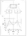
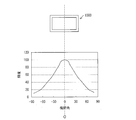
- the backlight has luminance directivity in the front direction of the display 1000 (viewing angle 0 ° in FIG. 14).
- the dual view display (hereinafter referred to as “DV display”) displayed on the DV display is centered on the display in the direction of the viewing angle of ⁇ 45 °.
- the backlight unit having the luminance directivity in the direction of the viewing angle of 0 ° shown in FIG. 14 is used for DV display, the luminance of the backlight light is reduced by about 60% around the viewing angle of ⁇ 45 °. As a result, the display quality deteriorates. Further, in order to increase the luminance in the vicinity of the viewing angle ⁇ 45 degrees, it is necessary to increase the luminance of the backlight as a whole, and there is a problem that the power consumption of the backlight is unnecessarily increased.
- Patent Document 1 discloses a backlight unit for a DV display (hereinafter simply referred to as “DV backlight unit”).
- FIG. 14 is a perspective view showing a configuration of a conventional DV backlight unit.
- the DV backlight units are arranged in order from the front side to the back side.
- a sheet 1015, a prism sheet 1014, a diffusion sheet 1013, a light guide plate 1012, and a reflection plate 1016 are provided. Further, a plurality of light sources 1011 are arranged along one side of the four sides of the light guide plate 1012.
- the prism forming surface of the prism sheet 1014 faces the side where the light guide plate 1012 is disposed, and its prism axis (prism ridgeline) is arranged in parallel along the vertical direction of the liquid crystal screen.
- the prism forming surface of the prism sheet 1015 faces the liquid crystal panel, and the prism axis is arranged so as to coincide with the horizontal direction of the liquid crystal screen.
- the light emitted from the light source 1011 enters the light guide plate 1012 from one side surface of the light guide plate 1012, and the incident light exits in a planar shape from one surface of the light guide plate 1012.
- Light emitted from the light guide plate 1012 is converted into light having luminance directivity in two directions by two prism sheets 1014 and 1015 that are incident through the diffusion sheet 1013, and is incident on a liquid crystal panel capable of DV display. To do.
- a backlight unit having a common configuration is preferable regardless of whether it is a small size, a medium size, or a large size, in order to simplify the design and reduce the cost for maintaining the manufacturing equipment.
- the light source 1011 is arranged along one side of one light guide plate 1012.
- the DV backlight unit shown in FIG. 14 when the DV backlight unit shown in FIG. 14 is enlarged, the color of the light in the vicinity of the light source 1012 and the light in the vicinity of the side surface away from the light source 1012 out of the light emitted in a planar shape from the light guide plate 1012. Therefore, the display quality is deteriorated.
- the present invention has been made in view of the above problems, and its object is to emit light having luminance directivity in a plurality of different directions without deterioration of display quality even when the size is increased. is there.
- the backlight unit of the present invention is a backlight unit having a light source and a light guide member, and the light source and the light guide member include the first and second light sources, 1 and a second light guide member, wherein the first light source is disposed on a side surface of the first light guide member, and the second light source is disposed on a side surface of the second light guide member.
- the first and second light sources are arranged to face each other via the first and second light guide members in a plan view, and further, the first or second light guide member is disposed.
- An optical path changing member for changing the optical path of the light passing therethrough which has an incident surface that directly emits light emitted from the light source and an output surface that directly emits incident light from the incident surface toward an external display panel It is characterized by having.
- the first and second light sources arranged to face each other via the first and second light guide members, and the first light source arranged on the side surface are the first.
- first and second light sources opposed to each other through the first and second light guide members are provided in a plan view, even if the size is increased, the distance between both side surfaces opposed in the plan view Can be prevented from changing, and display quality can be prevented from deteriorating.
- the backlight unit of the present invention is a backlight unit having a light source and a light guide member, and the light source and the light guide member include first and second light sources, and first and second light guide members, respectively.
- the first light source is disposed on a side surface of the first light guide member
- the second light source is disposed on a side surface of the second light guide member.
- the two light sources are arranged so as to face each other via the first and second light guide members in plan view, and further, are incident surfaces on which light emitted from the first or second light guide member is directly incident.
- an exit surface that directly emits incident light from the entrance surface toward an external display panel, and includes an optical path changing member that changes the optical path of the passing light.
- the display quality is not deteriorated even when the size is increased, and it is possible to emit light having luminance directivity in a plurality of different directions.
- FIG. 1 is a diagram illustrating an overall configuration of a display system according to an embodiment of the present invention.
- the state of DV display of the display system and the state of luminance of the displayed image are shown.
- FIGS. 1 to 12 An embodiment of the present invention will be described with reference to FIGS. 1 to 12 as follows. Descriptions of configurations other than those described in the following specific items may be omitted as necessary. However, in the case where they are described in other items, the configurations are the same. For convenience of explanation, members having the same functions as those shown in each item are given the same reference numerals, and the explanation thereof is omitted as appropriate.
- FIG. 1 is a diagram showing the overall configuration of the display system 100.
- a display system 100 has a liquid crystal panel (display panel) 5 having an image display area, a BL (backlight) unit 20 that illuminates the liquid crystal panel 5 from the back side, and an image display area.
- the frame 9 enclosing the liquid crystal panel 5 and the BL unit 20 and sensors (luminance sensors) 6A and 6B for detecting the amount of light emitted from the liquid crystal panel 5 are provided.
- the display system 100 includes a calculation unit 7, a light source drive control unit 8, and a memory 10 for controlling the light amounts of the light sources 4A and 4B in accordance with outputs from the sensors 6A and 6B.
- the BL unit 20 includes an optical path changing member 1 serving as an emission surface of the BL unit 20, a light guide plate (first light guide member) 2A, a light guide plate (second light guide member) 2B, and a reflection plate (reflection member). 3 and a light source (first light source) 4A and a light source (second light source) 4B. As will be described later, the BL unit 20 has luminance directivities in two different directions.
- the display system 100 is a display system capable of simultaneously displaying two or more images in different directions.
- the display system 100 can perform dual view display (hereinafter referred to as DV display) that displays two images simultaneously, or quartet view display (hereinafter referred to as CV display) that displays four images simultaneously. .
- DV display dual view display
- CV display quartet view display
- the display system 100 will be described as a display system that can mainly perform DV display.
- FIG. 2 shows a DV display state of the display system 100 and a luminance state of the displayed image.
- the display system 100 includes a right image IR that can be viewed when viewing the display system 100 from the right side and a left image IL that can be viewed when viewing the display system 100 from the left side. Both can be displayed simultaneously.
- the right image IR side (the right side of the drawing) may be referred to as “A side”
- the left image IL side (the left side of the drawing) may be referred to as “B side”.
- the light emitted from the display system 100 has a viewing angle of ⁇ 45 degrees and a brightness peaking at a peak angle while suppressing the brightness in the frontal direction (viewing angle direction 0 degree). It is comprised so that it may become.
- the viewing angle when viewing the display system 100 from the front is set to 0 degree
- the viewing angle from 0 degree to the A side is set to +
- the viewing angle from 0 degree to the B side viewing angle Is expressed as-.
- the right image IR which is an image with good display quality
- the left image IL can be viewed by the user on the B side.
- the display system 100 is not limited to DV display or CV display, and may be capable of 3D (stereoscopic) display.
- 3D stereo-dispelectron emission display
- the display system 100 for DV display by adjusting the relationship between the parallax barrier and the pixel structure from the display system 100 for DV display, a display system capable of 3D display for the naked eye without using 3D glasses can be obtained.
- the display system 100 will be described mainly as a display system capable of DV display.
- each component of the display system 100 will be described in order.
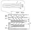
- FIG. 3 is a cross-sectional view showing the configuration of the liquid crystal panel 5 and the BL unit 20.
- the BL (backlight) unit 20 includes an optical path changing member 1, a light guide plate (first light guide member) 2A, a light guide plate (second light guide member) 2B, and a reflection plate (reflection member). 3), a light source (first light source) 4A, and a light source (second light source) 4B.
- front in the present specification means the surface on the side where the liquid crystal panel 5 displays an image (that is, the side on which the user views the liquid crystal panel 5).
- rear surface in the present specification means a surface opposite to the side on which the liquid crystal panel 5 displays an image.
- the BL unit 20 includes a liquid crystal panel 5, an optical path changing member 1, a light guide plate 2B, a light guide plate 2A, and a reflection plate 3 in order from the front side to the back side.
- the light source 4A is disposed on the side surface of the light guide plate 2A, and the light source 4B is disposed on the side surface of the light guide plate 2B.
- the light source 4A is disposed on one side (side surface) of the light guide plate 2A, and the light source 4B is disposed on one side (side surface) of the light guide plate 2B.
- the light sources 4A and 4B are disposed to face each other via the light guide plates 2A and 2B when the BL unit 20 is viewed in plan.
- the light guide plate 2A may be disposed on the front side, and the light guide plate 2B may be disposed on the back side.
- the BL unit 20 has a light source 4A and a light source 4B opposed to each other through the light guide plates 2A and 2B, a light guide plate 2A in which the light source 4A is arranged on one side, and a light source 4B on the side. Are disposed, and an optical path changing member 1 that changes the optical path of light passing therethrough.
- emission light A and B light having luminance directivity in which the luminance distribution in at least two directions different from the normal direction of the display screen of the liquid crystal panel 5 is maximized.
- emission light A and B light having luminance directivity in which the luminance distribution in at least two directions different from the normal direction of the display screen of the liquid crystal panel 5 is maximized.
- emission light A and B light having luminance directivity in which the luminance distribution in at least two directions different from the normal direction of the display screen of the liquid crystal panel 5 is maximized.
- the light can be emitted from the SUF2.
- the sidelight-type backlight is one in which light source light is incident from the side surface of the light guide, the incident light is reflected inside, and is emitted in a planar shape from the exit surface of the light guide.
- Patent Document 1 when only one light guide that emits light incident from one end face of the light guide in a planar shape is used, the size of the light guide is increased (the area is increased). The color of will change.
- a configuration in which light sources are provided on both sides of one light guide plate can be considered as the configuration of the backlight unit so as to have luminance directivity in two directions.
- FIG. 12 is a side view showing a state of the light guide plate in which the light sources 504A and 504B are arranged on the side surfaces facing each other.
- A) of FIG. 12 shows the state of the emitted light from the light guide plate in which the uneven pattern is sparse to dense from the right side to the left side of the paper, and (b) is the uneven pattern from dense to sparse from the central part to both side surfaces.
- C) shows the state of light emitted from a large light guide plate having a concavo-convex pattern from sparse to dense from the right side to the left side of the drawing.
- a light source 504A is disposed on one side surface of the opposite side surfaces of the light guide plate 502, and a light source 504B is disposed on the other side surface. ing.
- the concave / convex pattern is arranged from the side surface on the side where the light source 504B is arranged to the side surface on the side where the light source 504A is arranged so that the uneven pattern becomes dense. Has been.
- the uneven pattern is formed so that the in-plane luminance of the emitted light B emitted from the light source B is uniform.
- the light path through which the light emitted from the light sources 504A and 504B is guided in the light guide plate 502 is short.
- the light guide plate 502 even if the uneven pattern of the light guide plate 502 is aligned with the light source 504B (the light source 504B side is sparse and the light source 504A side is dense), the light emitted from the light source 504A Although it becomes weaker as it approaches the disposed side, it can reach the opposite side surface sufficiently and can be emitted as the emitted light A from the light emitting surface of the light guide plate 502.
- in-plane luminance variation is a problem.
- the concave / convex pattern of the light guide plate 502 is adjusted so that the central portion of the light guide plate 502 is dense and becomes sparse as it goes to both side surfaces. Then, the luminance variation in the surface of the emitted light A emitted from the light emitting surface of the light guide plate 502 from the light source 504A and the luminance variation in the surface of the emitted light B emitted from the light emitting surface of the light guide plate 502 from the light source 504B. Can be made equal.
- each of the outgoing light A and the outgoing light B can be adjusted by adjusting the concavo-convex pattern of the light guide plate even with a single light guide plate. In-plane luminance variation can be adjusted.
- the white light when the white light is repeatedly reflected a plurality of times in the light guide plate, the light amount on the low wavelength side gradually attenuates and the color changes. A smaller number of reflections is preferable.
- the light incident on the light guide plate 502 from the light sources 504A and 504B is sequentially emitted from the light exit surface as the exit light A and the exit light B, and is not reflected on the opposite side surface.
- the optical path length in the light guide plate 502 is short. For this reason, while uniforming the in-plane luminance variation of the emitted light A and B, all the light incident from the light sources 504A and 504B is emitted to the light emitting surface side of the light guide plate 502 up to the opposite side surface. I can't. For this reason, there is light reflected on a part of the opposite side surface.
- the optical path length inside the light guide plate 502 is short, so the light sources 504A and 504B enter the light guide plate 502.
- the number of reflections is small, and the change in the color of the light caused by reflection on the opposite side surfaces of the light sources 504A and 504B does not matter much. .
- the size of the light guide plate is small, even if the light guide plate 502 is a single light guide plate 502, by adjusting the concave / convex pattern, in-plane luminance variation can be suppressed, and there is no problem in color change. It is possible to emit a level of emitted light A and B.
- the optical path in the light guide plate 502 becomes long.
- the uneven pattern is sparsely and densely formed on the back surface of the large light guide plate 502 from the side surface on the side where the light source 504B is disposed to the side surface on the side where the light source 504A is disposed.
- the concave / convex pattern is formed so that the in-plane luminance of the emitted light B emitted from the light source 504B is uniform as in the light guide plate 502 of FIG.
- the optical path of the light guide plate 502 is short in the case of a small size, the outgoing light A has reached the side surface on which the light source 504B is arranged.
- the optical path of the light guide plate 502 is long, so A does not reach the side surface on which the light source 504B is disposed, and the emitted light A varies in luminance within the surface.
- the light is also reflected on the side surface opposite to the side surface on which each of the light sources 504A and 504B is disposed, and the emitted light Variations in the in-plane colors of A and outgoing light B increase.
- the BL unit 20 includes light sources 4A and 4B that are opposed to each other via the light guide plates 2A and 2B when viewed in plan. That is, since the light sources 4A and 4B are arranged on both side surfaces opposed to each other in plan view, the color between both side surfaces opposed to each other in plan view can be prevented from changing even when the size is increased (large area). Display quality can be prevented.
- the BL unit 20 includes two light guide plates 2A and 2B, and the uneven patterns of the light guide plates 2A and 2B can be individually adjusted. In-plane brightness variation and color variation can be suppressed.
- the BL unit 20 includes a plurality of light guide plates 2A and a light guide plate 2B. Therefore, by adjusting the uneven pattern on the back surface of each of the light guide plates 2A and 2B, each of the outgoing lights A and B is adjusted. It is possible to prevent in-plane variations in color while suppressing in-plane variations in luminance.
- the optical path changing member 1 is a kind of so-called optical sheet that plays a role of reflecting, diffusing, and condensing light emitted from the light guide plate 2, but the optical path changing member 1 of the present embodiment is at least its optical characteristics. Thus, the member changes the optical path of the transmitted light.
- the optical path changing member 1 includes a light incident surface (incident surface) SUF1 on which light emitted from the light guide plate 2B arranged facing the back surface is directly incident, and an incident light from the light incident surface SUF1.
- a light exit surface (exit surface) SUF2 that directly emits light toward the external liquid crystal panel 5 is provided.
- the light incident surface SUF1 and the light emitting surface SUF2 face each other in the vertical direction with respect to the paper surface.
- the light incident surface SUF1 may be flat or may have an uneven shape. That is, the BL unit 20 has a plurality of light sources 4A and 4B and a plurality of light guide plates 2A and 2B so as to have a luminance directivity in two directions. For this reason, as shown in FIG. 14, it is not necessary to provide the prism sheet 1014 having a convex shape toward the light guide plate 1013, and the light incident surface SUF1 can be made flat.
- the light incident surface SUF1 is not limited to be flat, and may have an uneven shape.
- the optical path changing member (optical sheet) 1 can be constituted by, for example, a diffusion sheet 1a shown in FIG. 4 or a lens sheet 1b shown in FIG.
- FIG. 4 is a diagram illustrating the light path of the BL unit 20 using the diffusion sheet 1a as the optical path changing member 1.
- FIG. 5 is a diagram illustrating the light path of the BL unit 20 using the lens sheet 1 b as the optical path changing member 1.
- the optical path changing member 1 has an emission angle ⁇ of light exiting from the light exit surface SUF ⁇ b> 2 of the optical path change member 1 and an exit angle ⁇ of light exiting from the light exit surface SUF ⁇ b> 4 ⁇ / b> B of the light guide plate 2 ⁇ / b> B.
- the optical characteristic is smaller than ( ⁇ ⁇ ).
- the light emitted from the light source 4 ⁇ / b> A has a luminance directivity in a direction inclined to the right side (A side, for example, viewing angle +45 degrees) with respect to the normal line of the light emission surface SUF ⁇ b> 2. It is possible to emit backlight light having On the other hand, the light emitted from the light source 4B can emit backlight light having luminance directivity in a direction inclined to the left side with respect to the normal line (B side, for example, a viewing angle of ⁇ 45 degrees). Yes.
- the light emitted from the light exit surface SUF2 of the optical path changing member 1 is directly applied to the external liquid crystal panel 5.
- the sheet-like member between the liquid crystal panel 5 and the light guide plate 2 ⁇ / b> B is composed of only one optical path changing member 1. Therefore, the optical path changing member (that is, the member existing between the light guide plate 2B and the liquid crystal panel 5) is smaller than the DV backlight unit described in Patent Document 1, and the utilization efficiency of the light emitted from the light guide plate 2B is reduced. Is expensive.
- FIG. 4A shows a state in which the light emitted from the light source 4A is emitted from the light emitting surface SUF4B of the light guide plate 2B and the light emitting surface SUF2 of the diffusion sheet 1a
- FIG. 4B illustrates the light emitted from the light source 4B.
- the state in which the emitted light is emitted from the light emitting surface SUF4B of the light guide plate 2B and the light emitting surface SUF2 of the diffusion sheet 1a is shown.
- the diffusing sheet 1a shown in FIG. 4 has a fine shape on the sheet surface (light incident surface SUF1 or light emitting surface SUF2) and a scattering material mixed therein, and generally has the above optical characteristics ( ⁇ ⁇ ⁇ ) has no direction dependency, but may be configured to have the above-described optical characteristics with respect to a specific direction.
- the above optical characteristics are given to the emission direction of the light sources 4A and 4B (in-plane direction of the diffusion sheet 1a). It is preferable.
- the diffusion sheet 1a is less isotropic than the lens sheet 1b described later when the optical characteristics are not direction-dependent, but conversely, the optical characteristics ( ⁇ ⁇ ) are isotropic. Since it can be said that it is provided, it is suitable as an optical path changing member 1 for CV display described later (FIG. 7).
- the light emitted from the light source 4A enters the light guide plate 2A from the side surface of the light guide plate 2A.
- the incident light exits from the light exit surface SUF4A of the light guide plate 2A, passes through the light guide plate 2B, exits from the light exit surface SUF4B of the light guide plate 2B at an exit angle ⁇ , and the exit light enters the diffusion sheet 1a.
- the exit light enters the diffusion sheet 1a.
- the diffusion sheet 1a then enters the light emitted from the light exit surface SUF4B of the light guide plate 2B at the exit angle ⁇ from the light incident surface SUF1, changes the angle of the incident light, and then exits from the light exit surface SUF2.
- the light is emitted at ⁇ ( ⁇ ⁇ ), and the emitted light is directly emitted to the liquid crystal panel 5.
- the light emitted from the light source 4B enters the light guide plate 2B from the side surface of the light guide plate 2B. Then, the incident light is emitted from the light exit surface SUF4B of the light guide plate 2B at an exit angle ⁇ , and the emitted light is incident on the diffusion sheet 1a.
- the diffusion sheet 1a then enters the light emitted from the light exit surface SUF4B of the light guide plate 2B at the exit angle ⁇ from the light incident surface SUF1, changes the angle of the incident light, and then exits from the light exit surface SUF2.
- the light is emitted at ⁇ ( ⁇ ⁇ ), and the emitted light is directly emitted to the liquid crystal panel 5.
- the diffusion sheet 1a of this embodiment is composed of a transparent resin as a base material (base material) and a light scattering agent (scattering fine particles) dispersed in the transparent resin.
- a thermoplastic resin for example, a thermosetting resin, or the like
- a polycarbonate resin an acrylic resin, a fluorine acrylic resin, a silicone acrylic resin, an epoxy acrylate Resins, polystyrene resins, cycloolefin polymers, methylstyrene resins, fluorene resins, polyethylene terephthalate (PET), polypropylene, acrylonitrile styrene copolymers, acrylonitrile polystyrene copolymers, and the like can be used.
- PET polyethylene terephthalate
- the light scattering agent scattering fine particles
- transparent fine particles made of an inorganic substance or a resin can be used.
- transparent fine particles made of an inorganic substance for example, fine particles made of an oxide such as silica (SiO 2 ), alumina (Al 2 O 3 ), magnesium oxide (MgO), titania, or other kinds such as calcium carbonate and barium sulfate. Fine particles can be used.
- Transparent fine particles made of resin include acrylic resin, styrene resin, acrylic styrene resin or a cross-linked product thereof; melamine formaldehyde resin; polytetrafluoroethylene, perfluoroalkoxy resin, tetrafluoroethylene-hexafluoropropylene copolymer, polyfluorovinylidene And particles made of a fluororesin such as ethylenetetrafluoroethylene copolymer; or a silicone resin can be used.
- the scattering fine particles having an average particle diameter (particle diameter) of the same order as the wavelength of visible light can contribute to light scattering. .
- the particle diameter of the scattering fine particles needs to be 100 nm or more. Further, in order to appropriately express the light scattering property, the particle diameter of each scattering fine particle is preferably on the order of larger than the wavelength of visible light, and is preferably 1 ⁇ m or more. Therefore, the average particle diameter of the scattering fine particles is preferably 1 ⁇ m or more, and more preferably about 2 ⁇ m.
- the fine particles for expressing the light scattering property are mixed in the transparent resin by about 5% by mass.
- the mixing ratio of the fine particles varies somewhat depending on the desired degree of light scattering (for example, defined by the haze value), but if it exceeds 5% by mass, the haze value increases unnecessarily.
- the distance that propagates through the diffusion sheet 1a is extended, and the transmittance is extremely lowered.
- the thickness of the diffusion sheet 1a is preferably 0.1 to 5 mm.
- the thickness of the diffusion sheet 1a is 0.1 to 5 mm, optimal light scattering properties and luminance can be obtained, which is preferable in terms of optical characteristics.
- the thickness is less than 0.1 mm, the desired light scattering property cannot be exhibited.
- the thickness exceeds 5 mm, the amount of resin is large, and thus the luminance is lowered due to absorption.
- the diffusion sheet 1a of the present embodiment has a haze value of 75% and a total light transmittance of 86%, but the haze value is 70% or more and the total light transmittance is 50% or more. Preferably there is.
- thermoplastic resin When a thermoplastic resin is used as the transparent resin, air bubbles may be used as the light scattering agent.
- the internal surface of the bubble formed inside the thermoplastic resin causes diffused reflection of light, and light scattering properties equivalent to or higher than when scattering particles are dispersed can be exhibited. Therefore, the film thickness of the diffusion sheet 1a can be made thinner.
- Examples of such a diffusion sheet 1a include white PET and white PP.
- White PET is a resin that is incompatible with PET, fillers such as titanium oxide (TiO 2 ), barium sulfate (BaSO 4 ), and calcium carbonate are dispersed in PET, and then the PET is stretched by a biaxial stretching method. By doing so, bubbles are generated around the filler to form.
- the diffusion sheet 1a made of a thermoplastic resin only needs to be stretched in at least one axial direction. This is because bubbles can be generated around the filler by stretching in at least one axial direction.
- thermoplastic resin examples include acrylonitrile polystyrene copolymer, polyethylene terephthalate (PET), polyethylene-2,6-naphthalate, polypropylene terephthalate, polybutylene terephthalate, cyclohexanedimethanol copolymer polyester resin, isophthalic acid copolymer polyester resin, Polyester resins such as sporoglycol copolymer polyester resin and fluorene copolymer polyester resin, polyolefin resins such as polyethylene, polypropylene, polymethylpentene, and alicyclic olefin copolymer resins, acrylic resins such as polymethyl methacrylate, polycarbonate, Polystyrene, polyamide, polyether, polyesteramide, polyetherester, polyvinyl chloride, cycloolefin polymer And their copolymers and component, also can be used as mixtures of these resins are not particularly limited.
- the thickness of the diffusion sheet 1a is preferably 25 to 500 ⁇ m.
- the thickness of the diffusion sheet 1a is less than 25 ⁇ m, it is not preferable because the sheet stiffness (strength) is insufficient and wrinkles are likely to occur in the manufacturing process and the frame 9. Also, when the thickness of the diffusion sheet 1a exceeds 500 ⁇ m, there is no particular problem with the optical characteristics, but it is difficult to process into a roll shape due to increased rigidity, and the slit cannot be easily formed. This is not preferable because the advantage of the thinness obtained is reduced.
- the diffusion sheet 1a may have a fine concavo-convex structure formed on the light incident surface SUF1 or the light emitting surface SUF2.
- a method of forming this fine concavo-convex structure when forming the diffusion sheet 1a, it is brought into close contact by applying pressure to a mold for shaping the fine concavo-convex structure by a coextrusion forming method or an injection molding method. There is a method of transferring the concavo-convex structure.
- the fine concavo-convex structure there is a method in which the light incident surface SUF1 or the light exit surface SUF2 of the diffusion sheet 1a is molded using a radiation curable resin such as UV (Ultra Violet) curable resin. More specifically, after the diffusion sheet 1a is formed as a plate-like member by a coextrusion method, a fine uneven structure is formed by UV forming an uneven shape on the light incident surface SUF1 or the light exit surface SUF2 of the diffusion sheet 1a. be able to.
- a radiation curable resin such as UV (Ultra Violet) curable resin.
- the surface state of the light incident surface SUF1 or the light exit surface SUF2 is often expressed by roughness as roughness, but here, the surface state is defined as haze value and unevenness spacing Sm value (hereinafter referred to as “Sm value”). It shows with.
- the haze value is defined by JIS K 7136, and is represented by an average value when measured five times using a haze meter.
- the Sm value is defined by the surface roughness standard JIS B0601-2001, and is a contact type surface roughness meter. Means an average value when measured under the condition of a cut-off value of 2.0 mm.
- the unevenness interval is fine but the unevenness roughness is insufficient, and the light surface scattering becomes weak. If it exceeds 900 ⁇ m, the unevenness interval is wide and the roughness becomes rough. Scattering becomes stronger, but it leads to lower front luminance.
- the surface roughness of the light incident surface SUF1 or the light exit surface SUF2 is regular, it is advantageous in obtaining a certain scattering effect as compared with the case where the surface roughness is irregular. It becomes easy.
- the surface condition of the mold is adjusted and transferred in-line during injection molding or extrusion molding. And a method of blasting an abrasive. Further, when the light scattering agent is bleed out under the extrusion conditions, the concentration and particle diameter of the scattering fine particles and the thickness of the scattering layer are adjusted.
- thermoplastic resin is heated and melted with an extruder, extruded from a T-die, and formed into a plate shape.
- the co-extrusion method is used in the case of a laminated plate, and a plurality of extruders are used to carry out lamination extrusion from a lamination die such as a feed block die or a manifold die to form a multilayer plate.
- FIG. 5A shows a state in which the light emitted from the light source 4A is emitted from the light emitting surface SUF4B of the light guide plate 2B and the light emitting surface SUF2 of the lens sheet 1b
- FIG. 5A shows a state in which the light emitted from the light source 4A is emitted from the light emitting surface SUF4B of the light guide plate 2B and the light emitting surface SUF2 of the lens sheet 1b
- FIG. 5B shows a state in which the light emitted from the light source 4A is emitted from the light emitting surface SUF4B of the light guide plate 2B and the light emitting surface SUF2 of the lens sheet 1b
- the lens sheet 1b has a plurality of prism rows 1c formed on the side of the light exit surface SUF2.
- the lens sheet 1b has an optical characteristic that makes the emission angle ⁇ of the light emitted from the light emission surface SUF2 smaller than the emission angle ⁇ of the light emitted from the light emission surface SUF4B of the light guide plate 2B.
- the ridge line (prism axis) of the prism row 1c is arranged perpendicular to the emission direction of the light sources 4A and 4B. For this reason, the magnitude of the emission angle ⁇ of the emitted light when the light incident on the lens sheet 1b at a predetermined incident angle along the propagation direction of the light emitted from the light sources 4A and 4B is emitted from the light exit surface SUF2 side is The light output from the light output surface SUF4B of the light guide plate 2B is smaller than the output angle ⁇ .
- the BL unit 20 having luminance directivity in a plurality of different directions is configured.
- the exit angle ⁇ from the lens sheet 1b can be controlled by adjusting the apex angle of the prism row 1c and the refractive index of the lens sheet 1b.
- the cross section of the prism row 1c is an isosceles triangle.
- the apex angle is about 80 to 100 degrees, and the refractive index is about 1.5.
- the emission angle ⁇ of the light guide plate 2B is 65 ⁇ 5 degrees
- the emission angle ⁇ 45 degrees of the lens sheet 1b can be realized.
- the emission angle ⁇ approaches 0 degrees.
- the light guide plate 2A receives light emitted from the light source 4A arranged on one end surface, emits the incident light from the light output surface SUF4A, and enters the light incident surface SUF1 of the optical path changing member 1 through the light guide plate 2B. It is a member that guides light to
- the light guide plate 2B receives light emitted from the light source 4B disposed on one end face, emits the incident light from the light exit surface SUF4B, and directly guides the light to the light entrance surface SUF1 of the optical path changing member 1 It is.
- the light guide plates 2A and 2B are transparent resin plates that convert linear light generated from the light sources 4A and 4B into a surface light source for entering the liquid crystal panel 5.
- the shape of the light guide plates 2A and 2B is a plate shape (cuboid shape), and the shape of the light exit surfaces SUF4A and 4B (bottom surfaces SUF5A and 5B) is a rectangular shape.
- the thickness of the light guide plates 2A and 2B is 0.2 mm to 3 mm, but the thickness of the light guide plates 2A and 2B is not limited to this range.
- the light incident on the light guide plate 2A from the light source 4A exits from the light exit surface SUF4A of the light guide plate 2A, passes through the light guide plate 2B, and has an angle corresponding to, for example, a viewing angle ⁇ + 70 degrees ⁇ 5 degrees.
- the light is emitted from the 2B emission surface SUF4B.
- the configuration of the BL unit 20 having the light guide plates 2A and 2B as described in the present embodiment allows the optical path to be changed.
- the effect of suppressing the luminance variation between the outgoing light A and the outgoing light B while reducing the deterioration of the luminance on the low wavelength side due to the increase in length can be obtained particularly remarkably.
- the panel size targeted by the BL unit 20 may be smaller than 20 inches. If the backlight is used for a panel size of 15 inches or more, the deterioration in luminance on the low wavelength side due to the longer optical path is reduced. However, it is possible to obtain an effect of suppressing variation in luminance between the outgoing light A and the outgoing light B.
- the light guide plates 2A and 2B are plate-shaped in this embodiment, but various shapes such as a wedge shape and a boat shape can be used. Moreover, as a constituent material of the light guide plates 2A and 2B, a synthetic resin having a high transmittance such as a methacrylic resin, an acrylic resin, a polycarbonate resin, a polyester resin, or a vinyl chloride resin can be used. As the light guide plates 2A and 2B, those in which the light exit surfaces SUF4A and 4B are mirror surfaces and the other bottom surfaces SUF5A and 5B are rough surfaces are used.
- the bottom surfaces SUF5A and 5B of the light guide plates 2A and 2B are subjected to prism (plural concavo-convex shape) processing, dot (plural concavo-convex shape) processing, and the like for uniform brightness and improved luminance.
- the light guide plates 2A and 2B can be adjusted so that the two light guide plates 2A and 2B can be adjusted by adjusting the refractive index, the arrangement of the prism patterns arranged on the bottom surfaces SUF5A and 5B, and the arrangement of the dot patterns. Even if they are overlapped, the emitted light from the light source 4A is emitted from the light emitting surface SUF4B of the light guide plate 2B at an angle ⁇ , and the emitted light from the light source 4B is emitted from the light emitting surface SUF4B of the light guide plate 2B at an angle ⁇ . It is supposed to be.
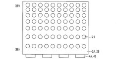
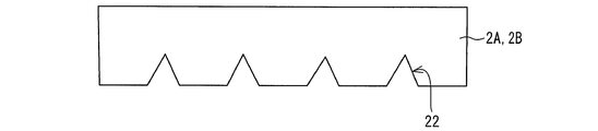
- FIG. 6 is a plan view showing the back surface of the light guide plates 2A and 2B subjected to dot processing.
- a plurality of dots 21 are formed on the back surfaces of the light guide plates 2A and 2B.
- each of the plurality of dots 21 has a hemispherical shape.
- the plurality of dots 21 On the back surface of the light guide plate 2A, the plurality of dots 21 have a low density from the side surface on the side where the light source 4A is arranged to the opposite side surface (side surface far from the light source 4A) facing the side surface. It is formed so as to be dense.
- a plurality of dots 21 has a density from the side surface on the side where the light source 4B is disposed to the opposite side surface (side surface far from the light source 4A) facing the side surface. Is formed from sparse to dense.
- the light incident on the light guide plate 2A from the light source 4A can be sequentially reflected by the plurality of dots 21 arranged on the back surface of the light guide plate 2A and can be incident on the optical path changing member 1.
- the light incident on the light guide plate 2B from the light source 4B can be sequentially reflected by the plurality of dots 21 arranged on the back surface of the light guide plate 2B and can be incident on the optical path changing member 1.
- BL unit 20 can be obtained.
- processing of the back surface of the light guide plates 2A and 2B is not limited to the hemispherical dots 21, but may be a prism shape (triangular pyramid shape) having a triangular cross section as shown in FIG.
- FIG. 7 is a cross-sectional view of the light guide plates 2A and 2B having prism-shaped processing formed on the back surface.
- an injection molding method in which the light guide plates 2A and 2B are formed by injection molding using a concavo-convex mold, or A pattern printing method in which a light guide member having a flat surface in advance is formed by injection molding or cast method, and dedicated ink is printed so as to make projections by screen printing can be exemplified.
- an injection molding method is generally used because it has a short tact and can be manufactured at low cost.
- the pattern printing method is generally used instead of the injection molding method because of the residual stress of the resin and the fact that cost merit cannot be achieved compared to the small size. Has been adopted.
- an uneven pattern is formed in order to form an uneven pattern in consideration of the effect of light reflected from the side facing the light source arranged on the side (the side far from the light source).
- the pattern density balance can be made relatively uniform in the plane.
- a light source is arranged on each of the opposing side surfaces of one light guide plate, and the density of the uneven pattern in the vicinity of one light source side is made sparse like the above uneven pattern, and the other light source
- the density of the uneven pattern in the vicinity of the side is made dense, the characteristics of light emitted from the light guide plate in different directions are different, and in-plane uniformity in perspective cannot be achieved.
- the BL unit 20 has different light guide plates 2A and 2B, the uneven and sparse / dense patterns arranged on the back surface are respectively optimized, and the outgoing light A (FIG. 3) is obtained. ) And outgoing light B (FIG. 3) can have the same characteristics.
- the reflecting plate 3 is a light reflecting member that reflects the light leaked from the bottom surface SUF5A of the light guide plate 2A.
- the surface shape of the reflecting plate 3 is a flat shape.
- the reflection plate 3 has a plate shape in this embodiment, but is not limited to a plate shape, and various shapes can be used.
- a film made of a polyester resin or a polyolefin resin, or a white film is used as a constituent material of the reflecting plate 3.
- a pigment such as titanium oxide, barium sulfate, calcium carbonate, aluminum hydroxide, magnesium carbonate, aluminum oxide is added to the plastic resin so as to be white. It is formed into a film or sheet. It is also possible to use a resin in which an inorganic filler such as calcium carbonate or titanium oxide is contained, a film is formed, and this is stretched to form a large number of microvoids.
- the light source 4A is provided at a position where light is emitted from the B side to the light guide plate 2A.
- the light source 4B is provided at a position where light is emitted from the A side to the light guide plate 2B. That is, as shown in FIG. 3, the light sources 4A and 4B are arranged on the left and right sides with respect to the paper surface.
- the direction in which the light from the light source 4A is emitted is the right direction (emitted light A in FIG. 3), and the direction in which the light from the light source 4B is emitted is the left direction (emitted light B in FIG. 3).
- the light sources 4A and 4B LEDs (Light Emitting Diodes) are used in the present embodiment, but a CCFT (Cold Cathode Fluorescent Tube) or a surface light source such as electroluminescence may be used. good.
- the light source is assumed to be at least two independent LEDs.
- the light sources 4A and 4B are CCFT, a U-shaped fluorescent tube may be used, and the single light tube in which the light source 4A and the light source 4B are connected to each other may be used.
- two L-shaped fluorescent tubes may be used in combination.
- the light sources 4A and 4B may include a reflector (not shown).
- the inner surface of the reflector has a parabolic shape, and the light sources 4A and 4B are arranged at the focal position.
- the liquid crystal panel 5 is a display panel that can simultaneously display a plurality of images. As shown in FIG. 3, the liquid crystal panel 5 has a light irradiation surface SUF3 to which light emitted from the light emission surface SUF4B of the light guide plate 2B is directly irradiated.
- the liquid crystal panel 5 is arranged in order from the front side to the back side.
- the polarizing plate 51, the parallax barrier (parallax barrier) 52, the adhesive layer 53, the CF (color filter) substrate 54, the TFT (thin film transistor) substrate 55, the polarization A plate 56 is provided.
- a liquid crystal layer (not shown) is arranged between the CF substrate 54 and the TFT substrate 55.
- the back surface of the display area located on the A side (the right side of the drawing) in the liquid crystal panel 5 is illuminated by light emitted from the optical path changing member 1 from the light source 4A through the light guide plates 2A and 2B.
- a luminance peak is obtained at a viewing angle of 45 degrees.
- the back surface of the display area located on the B side (the left side of the drawing) in the liquid crystal panel 5 is illuminated by light emitted from the optical path changing member 1 from the light source 4B through the light guide plate 2B.
- a luminance peak is obtained at a viewing angle of ⁇ 45 degrees.
- the luminance peak for the image displayed on the A side of the liquid crystal panel 5 and the luminance peak for the image displayed on the B side of the liquid crystal panel 5 are in different directions.
- the viewing angle at which the luminance peak can be obtained for each of the images displayed on the A side and the B side of the liquid crystal panel 5 can be set to a desired angle. It is possible to improve the display quality of the image.
- polarizing plates 51 and 56 are composed of a polarizing substrate containing a polarizing element, a base substrate (not shown) sandwiching the polarizing substrate between both sides, a protective film (not shown) on one side, and a polarizing plate on the other side. It is comprised from the release film (not shown) for affixing on a glass substrate.
- the polarizing plates 51 and 56 are as thin as about 0.12 mm to 0.4 mm even if about 10 layers are stacked.
- a polarizing substrate containing a polarizing element is iodine or a dichroic dye that is a polarizing element, which causes a polarizing effect.
- As the polarizing substrate polyvinyl alcohol (PVA, Poly Vinyle Alcohol) is used, and the polarizing element is included in this medium.
- Triacetyl cellulose (TAC, Triacetyl cellulose, Cellulose triacetate) is used as a base substrate for protecting the polarizing substrate.
- the release film is coated with an adhesive layer on the base substrate side, peeled off when applied to the glass substrate, and attached to the glass substrate with the adhesive layer.
- parallax barrier 52 Next, the parallax barrier 52 will be described with reference to FIGS.
- the parallax barrier 52 is an optical member in which a light transmission region and a blocking region are formed in a stripe shape, and the parallax barrier 52 separates a plurality of images to be displayed into individual display regions.
- FIG. 8 is a plan view of the liquid crystal panel 5 provided with a parallax barrier.
- FIG. 9 is a diagram illustrating how light is emitted to the A side and the B side of the liquid crystal panel 5.
- the parallax barrier 52 covers the right half of the pixels in the odd lines and the left half of the pixels in the even lines.
- An even line pixel in which the left half is covered with the parallax barrier 52 and the right half is exposed is referred to as a pixel 57A
- an odd line pixel in which the right half is covered with the parallax barrier 52 and the left half is exposed is referred to as a pixel 57B.
- the parallax barrier 52 covers half of the pixels, different images can be displayed on each of the pixels 57A and 57B (DV display), and different images can be viewed by the users on the A side and B side. .
- DV display can be performed by adjusting the parallax barrier 52 and the pixel configuration so that the viewing angle to the A side and the B side is ⁇ 45 degrees. Further, 3D display with the naked eye can be performed by adjusting the viewing angle to be ⁇ 6 degrees.
- the adhesive layer 53 shown in FIG. 3 is a transparent resin layer such as an acrylic resin that adheres the parallax barrier 52 and the CF substrate 54. Note that if the parallax barrier 52 and the CF substrate 54 are formed in contact with each other, the function as a parallax barrier cannot be exerted, so the adhesive layer 53 adjusts the distance between the parallax barrier 52 and the CF substrate 54 to an appropriate distance. This distance may be any distance that allows DV display.
- the CF substrate 54 shown in FIG. 3 has a colored layer or a black matrix (BM) that transmits red (R), green (G), and blue (B) light on the substrate in correspondence with each pixel. , Covered with a protective film.
- This colored layer is a coloring material or a colored film applied to the CF substrate 54 with a fine pattern, and a pigment-based or dye-based one is used.
- the BM layer prevents light leakage during black display and color mixing between adjacent colorants, and also prevents generation of photocurrent due to light irradiation to the TFT substrate 55.
- the photosensitive material is used for fixing the coloring material, it is mixed with the coloring material and fixed as it is.
- a thin BM layer of about 0.1 ⁇ m has a lot of metallic chromium, and carbon, titanium, nickel, etc. are also used.
- a high-definition screen has many stripe arrangements of colored layer patterns, but a low-definition screen has a good image quality with a good delta arrangement.
- the sensors 6A, 6B As shown in FIG. 1, the sensors 6 ⁇ / b> A and 6 ⁇ / b> B are provided on the front side of the liquid crystal panel 5, that is, the side on which the liquid crystal panel 5 displays an image, and are provided inside a frame frame 9 as a casing. Yes.
- the sensors 6A and 6B are luminance sensors that sense the luminance of light incident on the sensors 6A and 6B.
- the senor 6A is provided on the path of light emitted from the display area located on the left side (B side) of the liquid crystal panel 5.
- the sensor 6A measures the luminance of the light incident on it, and supplies the result of the measurement as detection data A to the calculation unit 7.
- the sensor 6B is provided on the path of light emitted from the display area located on the right side (A side) of the liquid crystal panel 5.
- the sensor 6B measures the luminance of the light incident on the sensor 6B, and supplies the result of the measurement to the calculation unit 7 as detection data B different from the detection data A.
- FIG. 10 is a block diagram illustrating a configuration of the display system 100 including the calculation unit 7.
- the calculation unit 7 includes a data analysis unit 71, a light source emission condition determination unit 72, and a calculation unit memory 73.
- the brightness of the incident light to the sensor 6A (left image IL in FIG. 2) is equal to the incident light to the sensor 6B (in FIG. 2).
- the luminance is higher than the luminance of the right image IR
- the data analysis unit 71 transmits a measurement command signal S_Enable_A to the sensor 6A.
- the data analysis unit 71 also transmits a measurement command signal S_Enable_B to the sensor 6B.
- the sensor 6A When the sensor 6A receives the measurement command signal S_Enable_A, the sensor 6A starts measuring the luminance, and transmits the measurement result to the data analysis unit 71 as detection data A.
- the sensor 6B receives the measurement command signal S_Enable_B, the sensor 6B starts measuring the luminance, and transmits the measurement result to the data analysis unit 71 as detection data B.
- the data analysis unit 71 receives the detection data A and B.
- the data analysis unit 71 transmits the analysis result A obtained by subjecting the detection data A to AD (Analog-Digital) conversion and noise removal to the light source emission condition determination unit 72.
- the data analysis unit 71 transmits the analysis result B obtained by performing AD conversion and noise removal on the detection data B to the light source emission condition determination unit 72.
- the light source emission condition determination unit 72 receives the analysis result A and the analysis result B.
- the light source emission condition determination unit 72 compares the brightness value measured by the sensor 6A indicated by the analysis result A and the brightness value measured by the sensor 6B indicated by the analysis result B.
- the luminance value measured by the sensor 6A indicated by the analysis result A is measured by the sensor 6B indicated by the analysis result B. It is larger than the brightness value.
- the calculation unit memory 73 is constituted by, for example, a ROM (Read Only Memory).
- a look-up table indicating the relationship between the result of the above-described size comparison and the increase / decrease in the current value applied to the light sources 4A and 4B is recorded in advance.
- the light source emission condition determination unit 72 reads the lookup table from the calculation unit memory 73.
- the look-up table includes information indicating that, when the luminance value indicated by the analysis result A is greater than the luminance value indicated by the analysis result B, the current value applied to the light source 4A is reduced by a predetermined value. It is out.
- the look-up table includes information indicating that when the luminance value indicated by the analysis result A is smaller than the luminance value indicated by the analysis result B, the current value applied to the light source 4A is increased by a predetermined value. Is included.
- the light source emission condition determination unit 72 controls the light emission condition setting value A to decrease or increase the current value applied to the light source 4A by a predetermined value according to the information included in the lookup table. Transmit to unit 8.
- the light emission condition setting value A is obtained by preliminarily setting the current value to be applied to the light source 4A to the light source drive control unit 8. The value is decreased by a predetermined value.
- the light emission condition setting value A is set in advance to the current value applied to the light source 4A to the light source drive control unit 8. The value is increased by a predetermined value.
- the light emission condition setting value A is the current applied to the light source 4A to the light source drive control unit 8. The value is reduced by a predetermined value.
- the look-up table includes information indicating that when the luminance value indicated by the analysis result A is larger than the luminance value indicated by the analysis result B, the current value applied to the light source 4B is increased by a predetermined value. May be included.
- the look-up table includes information indicating that when the luminance value indicated by the analysis result A is smaller than the luminance value indicated by the analysis result B, the current value applied to the light source 4B is decreased by a predetermined value. May be included.
- the light source light emission condition determining unit 72 uses the same principle as the light emission condition setting value A for increasing or decreasing the current value applied to the light source 4A, and the light emission condition setting value B for increasing or decreasing the current value applied to the light source 4B. Is transmitted to the light source drive control unit 8.
- the light source drive control unit 8 receives the light emission condition setting value A or the light emission condition setting value B.
- the light source drive control unit 8 can be constituted by, for example, a general LED drive circuit that drives the light sources 4A and 4B by supplying current to the light sources 4A and 4B.
- the light source drive control unit 8 can easily generate the light source control signal A, which is the current applied to the light source 4A, based on the light emission condition setting value A. That is, in this example, the light source drive control unit 8 may reduce the current value of the light source control signal A based on the light emission condition setting value A.
- the light source drive control unit 8 can easily generate the light source control signal B, which is the current applied to the light source 4B, based on the light emission condition setting value B. That is, in this example, the light source drive control unit 8 may increase the current value of the light source control signal B based on the light emission condition setting value B.
- the difference between the luminance value indicated by the analysis result A and the luminance value indicated by the analysis result B is a certain value (for example, the current value applied to the light source 4A or 4B in one operation).
- the value is less than the value to be increased or decreased, the operation is terminated.
- the difference between the brightness value indicated by the analysis result A (the brightness value measured by the sensor 6A) and the brightness value indicated by the analysis result B (the brightness value measured by the sensor 6B) refer to the analysis results A and B. Then, the light source emission condition determination unit 72 may obtain it.
- the drive control of the light sources 4A and 4B described above is current control in which the amplitude of the current applied to each of the light sources 4A and 4B is variable.
- PWM Pulse Width Modulation
- the display system 100 can achieve the same effect as that in the case where the drive control described above is performed even when the drive control of the light sources 4A and 4B is PWM. Such PWM control will be described.
- the calculation unit memory 73 the result of comparing the brightness value indicated by the analysis result A and the brightness value indicated by the analysis result B, and the pulse applied to the light sources 4A and 4B during one cycle.
- a look-up table showing the relationship with width expansion and contraction is recorded in advance.
- the “pulse width during one period of current” is simply referred to as “current pulse width”.
- the light source emission condition determination unit 72 reads the lookup table from the calculation unit memory 73.
- the look-up table includes information indicating that when the luminance value indicated by the analysis result A is greater than the luminance value indicated by the analysis result B, the pulse width of the current applied to the light source 4A is reduced by a predetermined width. Contains. Further, the lookup table indicates that when the luminance value indicated by the analysis result A is smaller than the luminance value indicated by the analysis result B, the pulse width of the current applied to the light source 4A is extended by a predetermined width. Contains information.
- the light source light emission condition determination unit 72 performs light source drive control on the light emission condition setting value A that expands or contracts the pulse width of the current applied to the light source 4A by a predetermined width according to the information included in the lookup table. Transmit to unit 8.
- the light emission condition setting value A indicates the pulse width of the current applied to the light source 4A to the light source drive control unit 8. , A value to be reduced by a predetermined width.
- the light emission condition setting value A indicates the pulse width of the current applied to the light source 4A to the light source drive control unit 8. , A value that extends by a predetermined width.
- the look-up table indicates that when the luminance value indicated by the analysis result A is larger than the luminance value indicated by the analysis result B, the pulse width of the current applied to the light source 4B is extended by a predetermined width. Information may be included.
- the lookup table indicates that when the luminance value indicated by the analysis result A is smaller than the luminance value indicated by the analysis result B, the pulse width of the current applied to the light source 4B is reduced by a predetermined width.
- Information may be included.
- the light source light emission condition determining unit 72 uses the same principle as the light emission condition setting value A for expanding and contracting the pulse width of the current applied to the light source 4A, and the light emission condition setting value B for expanding and contracting the pulse width of the current applied to the light source 4B. Is transmitted to the light source drive control unit 8.
- the light source drive control unit 8 receives the light emission condition setting value A or the light emission condition setting value B.
- the light source drive control unit 8 can be configured by, for example, a general LED drive circuit that drives the light sources 4A and 4B by supplying a current subjected to PWM modulation to the light sources 4A and 4B.
- the light source drive control unit 8 can easily generate the light source control signal A, which is the current applied to the light source 4A, based on the light emission condition setting value A. That is, the light source drive control unit 8 may expand or contract the pulse width of the current of the light source control signal A based on the light emission condition setting value A.
- the light source drive control unit 8 can easily generate the light source control signal B, which is the current applied to the light source 4B, based on the light emission condition setting value B. That is, the light source drive control unit 8 may expand or contract the pulse width of the current of the light source control signal B based on the light emission condition setting value B.
- the difference between the luminance value indicated by the analysis result A and the luminance value indicated by the analysis result B is a certain value (for example, a value corresponding to the pulse width of the current that is expanded or contracted by one operation). ) When it becomes less than, the operation is terminated.
- the difference between the brightness value indicated by the analysis result A (the brightness value measured by the sensor 6A) and the brightness value indicated by the analysis result B (the brightness value measured by the sensor 6B) refer to the analysis results A and B. Then, the light source emission condition determination unit 72 may obtain it.
- the display system 100 can achieve the effects described above even when the drive control of the light sources 4A and 4B is PWM.
- the light source drive control unit 8 may be configured to be able to read information recorded in the memory 10 and record information in the memory 10.
- the position where the memory 10 is provided may be in the backlight unit 300 or in another display device unit 200 (see FIG. 2).
- the solid state variation between the light source 4A and the light source 4B, the visual characteristics of the liquid crystal panel 5 are asymmetrical, the positional deviation of the parallax barrier 52, and the like.
- these luminances can be made substantially uniform.
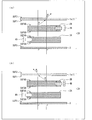
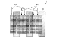
- FIG. 11 is a diagram showing a BL unit (backlight unit) 20c, which is still another configuration example of the backlight unit.
- the BL unit 20c is different from the BL unit 20 in that light sources are arranged along two sides (side surfaces) of the light guide plates 2A and 2B.
- light sources 4A and 4C are arranged on each of two adjacent sides of the light guide plate 2A.
- a light source is provided on each of the side facing the side where the light source 4A is disposed and the side facing the one side where the light source (first light source, second light source) 4C is disposed. Is not arranged.
- light sources 4B and 4D are arranged on each of the adjacent sides of the light guide plate 2B.
- the light source 4A, 4B, 4C, and 4D are arranged on each of the four sides (side surfaces) of the BL unit 20c when viewed in plan.
- the BL unit 20c it is possible to realize a backlight suitable for CV display in which different images are displayed in the four directions of left and right and up and down.
- the above-described optical characteristic ( ⁇ ⁇ ) has no direction dependency, or the direction from the left side to the right side (right side to left side) in plan view.
- the backlight unit of the present invention is a backlight unit having a light source and a light guide member in order to solve the above problems, and the light source and the light guide member are first and first, respectively.
- the first light source and the second light source are arranged opposite to each other via the first light guide member and the first light source member in plan view, and are arranged on the side surface of the optical member. 2 having an incident surface directly incident on the light emitted from the light guide member 2 and an output surface directly emitting the incident light from the incident surface toward the external display panel, and changing the optical path of the light passing therethrough
- An optical path changing member is provided.
- the first and second light sources arranged to face each other via the first and second light guide members, and the first light source arranged on the side surface are the first.
- first and second light sources opposed to each other through the first and second light guide members are provided in a plan view, even if the size is increased, the distance between both side surfaces opposed in the plan view Can be prevented from changing, and display quality can be prevented from deteriorating.
- the first and second light guide members are preferably arranged so as to overlap each other in plan view.
- a plurality of uneven shapes are formed on the back surfaces of the first and second light guide members, and the plurality of uneven shapes are formed on the back surface of the first light guide member.
- the density is formed from sparse to dense, and on the back surface of the second light guide member, It is preferable that the density be formed from sparse to dense from the side surface on the side where the second light source is disposed to the opposite side surface facing the side surface.
- the light path is changed by sequentially reflecting the light incident on the first light guide member from the first light source by the plurality of uneven shapes arranged on the back surface of the first light guide member.
- the light is incident on the member, and the light incident on the second light guide member from the second light source is sequentially reflected by the plurality of concave and convex shapes disposed on the back surface of the second light guide member, so that the optical path It can enter into a change member.
- the uneven shape may be a hemispherical shape or a triangular pyramid shape.
- a plurality of prism rows are formed on the emission surface of the optical path changing member, and the axis of each prism row is perpendicular to the emission directions of the first and second light sources.
- the emission angle of the emitted light when the light incident on the optical path changing member at a predetermined incident angle along the emission direction of the first and second light sources is emitted from the emission surface is It becomes smaller than the incident angle. For this reason, a backlight unit having luminance directivity in a plurality of different directions can be obtained.
- the optical path changing member preferably includes scattering fine particles that scatter light.
- the total light transmittance and the haze value are adjusted to desired values by appropriately adjusting the constituent material of the base material, the constituent material of the scattering fine particles, the average particle diameter (particle diameter), and the mixing rate. can do.
- the above optical characteristics have no direction dependency, but conversely, it can be said that the above optical characteristics are provided isotropically.
- CV display a backlight unit suitable for so-called quartet view display
- the display device of the present invention the backlight unit, the display panel that displays information on the display screen by receiving light emitted from the emission surface of the optical path changing member provided in the backlight unit, It is preferable to provide.
- the display panel has at least two luminance sensors that are installed in at least two directions different from the normal direction of the display screen and detect the luminance of light emitted from the display screen, and the two luminance sensors.
- a light source drive control unit that adjusts the magnitude of the current supplied to each of the first and second light sources so that the difference in luminance between the detected lights is smaller than a predetermined luminance difference. Preferably it is.
- the light source drive control unit supplies the current to each of the first and second light sources so that the difference in luminance between the lights detected by the two luminance sensors is smaller than the predetermined luminance difference. Adjust the size of. Therefore, it is possible to suppress in-plane luminance variations caused by variations in the first and second light sources.
- the present invention can be used for a backlight unit or a display device that requires the backlight unit.
- Optical path changing member 1a Diffusion sheet (optical path changing member) 1b Lens sheet (optical path changing member) 1c Prism row 2A
- Calculation unit 8 Light source drive control unit 20 BL unit (backlight unit) 20c BL unit (backlight unit) 21 dots (multiple irregular shapes)
- 100 Display system (display device) SUF1 Light incident surface (incident surface) SUF2 light exit surface (exit surface) SUF4A light exit surface SUF4B light exit surface SUF5A bottom surface SUF5B bottom surface
Landscapes
- Physics & Mathematics (AREA)
- General Physics & Mathematics (AREA)
- Optics & Photonics (AREA)
- Engineering & Computer Science (AREA)
- Computer Hardware Design (AREA)
- Theoretical Computer Science (AREA)
- Planar Illumination Modules (AREA)
Abstract
L'unité de rétroéclairage (BL) (20) de l'invention est équipée de sources de lumière (4A, 4B), et de plaques de guidage de lumière (2A, 2B). La source de lumière (4A) est placée sur une face latérale de la plaque de guidage de lumière (2A). La source de lumière (4B) est placée sur une face latérale de la plaque de guidage de lumière (2B). Selon une vue en plan, les sources de lumière (4A, 4B) sont disposées face à face avec les plaques de guidage de lumière (2A, 2B) pour intermédiaire. En outre, l'objet de l'invention possède : une face incidence de lumière (SUF1) sur laquelle la lumière émise en sortie par la plaques de guidage de lumière (2A) ou la plaque de guidage de lumière (2B) est directement incidente; et une face d'émission en sortie de lumière (SUF2) qui émet en sortie de manière directe la lumière incidente provenant de la face incidence de lumière (SUF1) et l'oriente vers un panneau à cristaux liquides (5) d'une partie externe. L'objet de l'invention est également équipé d'un élément de modification de trajet lumineux (1) qui modifie un trajet lumineux que la lumière traverse. Par conséquent, une lumière dotée de propriétés d'orientation de luminosité dans une pluralité de directions différentes, est émise sans détérioration de la qualité visuelle y compris dans le cas d'une augmentation des dimensions.
Priority Applications (1)
| Application Number | Priority Date | Filing Date | Title |
|---|---|---|---|
| US14/112,327 US20140043377A1 (en) | 2011-04-22 | 2012-04-16 | Backlight unit and display device |
Applications Claiming Priority (2)
| Application Number | Priority Date | Filing Date | Title |
|---|---|---|---|
| JP2011096583 | 2011-04-22 | ||
| JP2011-096583 | 2011-04-22 |
Publications (1)
| Publication Number | Publication Date |
|---|---|
| WO2012144449A1 true WO2012144449A1 (fr) | 2012-10-26 |
Family
ID=47041555
Family Applications (1)
| Application Number | Title | Priority Date | Filing Date |
|---|---|---|---|
| PCT/JP2012/060238 Ceased WO2012144449A1 (fr) | 2011-04-22 | 2012-04-16 | Unité de rétroéclairage, et dispositif d'affichage |
Country Status (2)
| Country | Link |
|---|---|
| US (1) | US20140043377A1 (fr) |
| WO (1) | WO2012144449A1 (fr) |
Families Citing this family (17)
| Publication number | Priority date | Publication date | Assignee | Title |
|---|---|---|---|---|
| CN104460115B (zh) * | 2014-12-31 | 2017-09-01 | 苏州大学 | 一种多视角像素指向型背光模组及裸眼3d显示装置 |
| TW201627964A (zh) * | 2015-01-26 | 2016-08-01 | 廣達電腦股份有限公司 | 可出現光紋圖案之電子裝置 |
| TWI588550B (zh) * | 2015-02-17 | 2017-06-21 | 元太科技工業股份有限公司 | 顯示裝置 |
| US20170010407A1 (en) * | 2015-07-09 | 2017-01-12 | Apple Inc. | Displays With Multimode Backlight Units |
| CN104991753B (zh) * | 2015-08-03 | 2019-07-26 | 联想(北京)有限公司 | 控制方法、控制装置及电子设备 |
| CN107179627B (zh) * | 2016-03-09 | 2020-10-23 | 台湾扬昕股份有限公司 | 光源模块以及显示装置 |
| CN105911746B (zh) * | 2016-06-29 | 2017-10-13 | 京东方科技集团股份有限公司 | 显示装置及其视角切换方法 |
| CN206301061U (zh) * | 2017-01-04 | 2017-07-04 | 京东方科技集团股份有限公司 | 一种背光模组及显示装置 |
| US10372196B2 (en) * | 2017-04-01 | 2019-08-06 | Intel Corporation | Dynamic pixel density adjustment |
| US10606076B2 (en) * | 2017-08-01 | 2020-03-31 | Visteon Global Technologies, Inc. | Dual-image head-up display |
| WO2019242208A1 (fr) * | 2018-06-22 | 2019-12-26 | 张家港康得新光电材料有限公司 | Structure et procédé permettant de réaliser la 3d à l'œil nu et la 2d/3d commutable |
| KR102587654B1 (ko) * | 2018-10-18 | 2023-10-11 | 삼성디스플레이 주식회사 | 백라이트 유닛 및 이를 포함하는 표시 장치 |
| CN110824775B (zh) * | 2019-11-27 | 2022-04-15 | 京东方科技集团股份有限公司 | 背光模组、显示装置及电子设备 |
| CN111176016B (zh) * | 2020-01-07 | 2022-10-18 | 京东方科技集团股份有限公司 | 一种背光模组和显示装置 |
| US11734436B2 (en) | 2021-06-25 | 2023-08-22 | Intel Corporation | Organic light emitting diode (OLED) compensation based on protected content |
| KR102522095B1 (ko) * | 2021-09-29 | 2023-04-17 | 엘지디스플레이 주식회사 | 표시 장치 |
| WO2023151087A1 (fr) * | 2022-02-14 | 2023-08-17 | 京东方科技集团股份有限公司 | Ensemble de rétroéclairage et appareil d'affichage |
Citations (7)
| Publication number | Priority date | Publication date | Assignee | Title |
|---|---|---|---|---|
| JP2006235288A (ja) * | 2005-02-25 | 2006-09-07 | Casio Comput Co Ltd | 表示装置及びそれに用いるバックライト |
| JP2008077946A (ja) * | 2006-09-20 | 2008-04-03 | Citizen Electronics Co Ltd | バックライトユニット及びそれを備えた表示装置 |
| JP2008204874A (ja) * | 2007-02-21 | 2008-09-04 | Fujifilm Corp | 面状照明装置 |
| JP2010020961A (ja) * | 2008-07-09 | 2010-01-28 | Citizen Electronics Co Ltd | 面状光源及び液晶表示装置 |
| JP2010177130A (ja) * | 2009-01-30 | 2010-08-12 | Keiwa Inc | 導光シート及びこれを用いたバックライトユニット |
| JP2011014520A (ja) * | 2008-12-04 | 2011-01-20 | Seiko Instruments Inc | 照明装置及び表示装置 |
| JP2011258458A (ja) * | 2010-06-10 | 2011-12-22 | Mitsubishi Electric Corp | バックライト装置および液晶表示装置 |
Family Cites Families (3)
| Publication number | Priority date | Publication date | Assignee | Title |
|---|---|---|---|---|
| JP2002050219A (ja) * | 2000-07-25 | 2002-02-15 | Internatl Business Mach Corp <Ibm> | 面状光源装置、導光板、表示装置 |
| US20100157625A1 (en) * | 2008-12-23 | 2010-06-24 | Mai Chien-Chin | Method for displaying multiple views |
| US20100231498A1 (en) * | 2009-03-13 | 2010-09-16 | Microsoft Corporation | Image display via multiple light guide sections |
-
2012
- 2012-04-16 WO PCT/JP2012/060238 patent/WO2012144449A1/fr not_active Ceased
- 2012-04-16 US US14/112,327 patent/US20140043377A1/en not_active Abandoned
Patent Citations (7)
| Publication number | Priority date | Publication date | Assignee | Title |
|---|---|---|---|---|
| JP2006235288A (ja) * | 2005-02-25 | 2006-09-07 | Casio Comput Co Ltd | 表示装置及びそれに用いるバックライト |
| JP2008077946A (ja) * | 2006-09-20 | 2008-04-03 | Citizen Electronics Co Ltd | バックライトユニット及びそれを備えた表示装置 |
| JP2008204874A (ja) * | 2007-02-21 | 2008-09-04 | Fujifilm Corp | 面状照明装置 |
| JP2010020961A (ja) * | 2008-07-09 | 2010-01-28 | Citizen Electronics Co Ltd | 面状光源及び液晶表示装置 |
| JP2011014520A (ja) * | 2008-12-04 | 2011-01-20 | Seiko Instruments Inc | 照明装置及び表示装置 |
| JP2010177130A (ja) * | 2009-01-30 | 2010-08-12 | Keiwa Inc | 導光シート及びこれを用いたバックライトユニット |
| JP2011258458A (ja) * | 2010-06-10 | 2011-12-22 | Mitsubishi Electric Corp | バックライト装置および液晶表示装置 |
Also Published As
| Publication number | Publication date |
|---|---|
| US20140043377A1 (en) | 2014-02-13 |
Similar Documents
| Publication | Publication Date | Title |
|---|---|---|
| WO2012144449A1 (fr) | Unité de rétroéclairage, et dispositif d'affichage | |
| US20140246982A1 (en) | Display device, and display device control method | |
| US20160187699A1 (en) | Liquid crystal display module and liquid crystal display comprising the same | |
| WO2007020966A1 (fr) | Dispositif d'éclairage planaire | |
| JP2009170205A (ja) | 導光板、導光板連結体、バックライトユニット、及び表示装置 | |
| JP2011197656A (ja) | 液晶表示装置 | |
| JP2003279712A (ja) | 透明ポリマーフィルム | |
| JP2006208930A (ja) | 光学シートとそれを用いたバックライト・ユニットおよびディスプレイ | |
| JP5217363B2 (ja) | レンズシート、ディスプレイ用光学シートおよびそれを用いたバックライトユニット、ディスプレイ装置 | |
| JP5104459B2 (ja) | 光学部材とそれを用いたバックライト・ユニット、ディスプレイ | |
| JP2009098566A (ja) | 光学シートおよびその製造方法 | |
| JP2010044270A (ja) | 光拡散板、光学シート、バックライトユニット及びディスプレイ装置 | |
| JP2010078980A (ja) | 光制御スタック及びそれを用いたバックライトユニット、表示装置 | |
| JP5245659B2 (ja) | 光デバイス、光均一デバイス、バックライトユニットおよびディスプレイ装置 | |
| CN100590349C (zh) | 面状照明装置 | |
| JP2011033643A (ja) | 光路変更シート、バックライトユニット及びディスプレイ装置 | |
| JP4956933B2 (ja) | 光学シートとそれを用いたバックライト・ユニットおよびディスプレイ | |
| JP2009210749A (ja) | 光学シート、これを用いたディスプレイ用バックライト・ユニットおよびディスプレイ | |
| WO2012144451A1 (fr) | Dispositif d'éclairage, et dispositif d'affichage | |
| JP5332469B2 (ja) | 光学部品、バックライトユニット及び表示装置 | |
| JP2012104266A (ja) | 導光板、バックライトユニット、及び表示装置 | |
| JP6195882B2 (ja) | 突起を有する光透過板 | |
| JP2014086387A (ja) | 導光板、導光板を備えたバックライトユニットおよび表示装置 | |
| WO2012144468A1 (fr) | Unité de rétroéclairage, et dispositif d'affichage | |
| JP2010122372A (ja) | 光学機能部材、バックライトユニット及びディスプレイ装置 |
Legal Events
| Date | Code | Title | Description |
|---|---|---|---|
| 121 | Ep: the epo has been informed by wipo that ep was designated in this application |
Ref document number: 12774143 Country of ref document: EP Kind code of ref document: A1 |
|
| WWE | Wipo information: entry into national phase |
Ref document number: 14112327 Country of ref document: US |
|
| NENP | Non-entry into the national phase |
Ref country code: DE |
|
| 122 | Ep: pct application non-entry in european phase |
Ref document number: 12774143 Country of ref document: EP Kind code of ref document: A1 |
|
| NENP | Non-entry into the national phase |
Ref country code: JP |