WO2012144686A1 - 단일상 형광체를 포함하는 백색 발광 다이오드 - Google Patents
단일상 형광체를 포함하는 백색 발광 다이오드 Download PDFInfo
- Publication number
- WO2012144686A1 WO2012144686A1 PCT/KR2011/003675 KR2011003675W WO2012144686A1 WO 2012144686 A1 WO2012144686 A1 WO 2012144686A1 KR 2011003675 W KR2011003675 W KR 2011003675W WO 2012144686 A1 WO2012144686 A1 WO 2012144686A1
- Authority
- WO
- WIPO (PCT)
- Prior art keywords
- phosphor
- white light
- emitting diode
- light emitting
- wavelength
- Prior art date
- Legal status (The legal status is an assumption and is not a legal conclusion. Google has not performed a legal analysis and makes no representation as to the accuracy of the status listed.)
- Ceased
Links
Images

Classifications
-
- H—ELECTRICITY
- H10—SEMICONDUCTOR DEVICES; ELECTRIC SOLID-STATE DEVICES NOT OTHERWISE PROVIDED FOR
- H10H—INORGANIC LIGHT-EMITTING SEMICONDUCTOR DEVICES HAVING POTENTIAL BARRIERS
- H10H20/00—Individual inorganic light-emitting semiconductor devices having potential barriers, e.g. light-emitting diodes [LED]
- H10H20/80—Constructional details
- H10H20/85—Packages
- H10H20/851—Wavelength conversion means
- H10H20/8511—Wavelength conversion means characterised by their material, e.g. binder
- H10H20/8512—Wavelength conversion materials
-
- H—ELECTRICITY
- H10—SEMICONDUCTOR DEVICES; ELECTRIC SOLID-STATE DEVICES NOT OTHERWISE PROVIDED FOR
- H10H—INORGANIC LIGHT-EMITTING SEMICONDUCTOR DEVICES HAVING POTENTIAL BARRIERS
- H10H20/00—Individual inorganic light-emitting semiconductor devices having potential barriers, e.g. light-emitting diodes [LED]
- H10H20/80—Constructional details
- H10H20/85—Packages
- H10H20/851—Wavelength conversion means
-
- C—CHEMISTRY; METALLURGY
- C09—DYES; PAINTS; POLISHES; NATURAL RESINS; ADHESIVES; COMPOSITIONS NOT OTHERWISE PROVIDED FOR; APPLICATIONS OF MATERIALS NOT OTHERWISE PROVIDED FOR
- C09K—MATERIALS FOR MISCELLANEOUS APPLICATIONS, NOT PROVIDED FOR ELSEWHERE
- C09K11/00—Luminescent materials, e.g. electroluminescent or chemiluminescent
- C09K11/08—Luminescent materials, e.g. electroluminescent or chemiluminescent containing inorganic luminescent materials
- C09K11/77—Luminescent materials, e.g. electroluminescent or chemiluminescent containing inorganic luminescent materials containing rare earth metals
- C09K11/7766—Luminescent materials, e.g. electroluminescent or chemiluminescent containing inorganic luminescent materials containing rare earth metals containing two or more rare earth metals
- C09K11/7774—Aluminates
-
- C—CHEMISTRY; METALLURGY
- C09—DYES; PAINTS; POLISHES; NATURAL RESINS; ADHESIVES; COMPOSITIONS NOT OTHERWISE PROVIDED FOR; APPLICATIONS OF MATERIALS NOT OTHERWISE PROVIDED FOR
- C09K—MATERIALS FOR MISCELLANEOUS APPLICATIONS, NOT PROVIDED FOR ELSEWHERE
- C09K11/00—Luminescent materials, e.g. electroluminescent or chemiluminescent
- C09K11/08—Luminescent materials, e.g. electroluminescent or chemiluminescent containing inorganic luminescent materials
- C09K11/77—Luminescent materials, e.g. electroluminescent or chemiluminescent containing inorganic luminescent materials containing rare earth metals
- C09K11/7766—Luminescent materials, e.g. electroluminescent or chemiluminescent containing inorganic luminescent materials containing rare earth metals containing two or more rare earth metals
- C09K11/7776—Vanadates; Chromates; Molybdates; Tungstates
-
- Y—GENERAL TAGGING OF NEW TECHNOLOGICAL DEVELOPMENTS; GENERAL TAGGING OF CROSS-SECTIONAL TECHNOLOGIES SPANNING OVER SEVERAL SECTIONS OF THE IPC; TECHNICAL SUBJECTS COVERED BY FORMER USPC CROSS-REFERENCE ART COLLECTIONS [XRACs] AND DIGESTS
- Y02—TECHNOLOGIES OR APPLICATIONS FOR MITIGATION OR ADAPTATION AGAINST CLIMATE CHANGE
- Y02B—CLIMATE CHANGE MITIGATION TECHNOLOGIES RELATED TO BUILDINGS, e.g. HOUSING, HOUSE APPLIANCES OR RELATED END-USER APPLICATIONS
- Y02B20/00—Energy efficient lighting technologies, e.g. halogen lamps or gas discharge lamps
Definitions
- the present invention relates to a white light emitting diode including a single phase phosphor.
- a single phase phosphor capable of emitting warm white using a single phase phosphor based on gadolinium (Gd), a rare earth metal ion of garnet type, is provided. It relates to a white light emitting diode comprising.
- a white LED using a light emitting device has attracted attention as a white light source for illumination or a white light source of a backlight unit.
- a YAG: Ce (yttrium aluminum garnet) phosphor is mainly used.
- the white LED using the YAG: Ce phosphor has the following characteristics.
- the excitation wavelength variable depends on the concentration of YAG: Ce, and has the advantage of high efficiency of the raw material for phosphor synthesis.
- the YAG: Ce phosphor has a disadvantage in that the practicality of the Y 3 Al 5 O 12 structure, that is, the color invariance is poor.
- particle size which is a standard of known phosphors, can be synthesized only at very high temperature, and has a disadvantage of forming a very narrow spectral band with a fluorescent excitation wavelength of 445 to 465 nm.
- the phosphor using TAG is a very expensive starting material (tebium oxide ( ⁇ b 4 O 7 )), there is a disadvantage that the unit price of the product increases. In addition, there is a problem that the brightness is about 20% lower than that of the phosphor based on the conventional YAG: Ce.
- the present invention is to solve the above-mentioned problems, to provide a white light emitting diode comprising a single-phase phosphor that emits warm white light, and has a high light efficiency.
- the present invention is to provide a white light emitting diode comprising a single-phase phosphor which can obtain a light emission wavelength of 1cd luminous intensity in the axial direction.
- the present invention is to provide a white light emitting diode comprising a single-phase phosphor having a color rendering index of Ra ⁇ 75 or more and a relatively low raw material cost.
- the present invention provides a white light emitting diode comprising a single phase phosphor, comprising a phosphor which is a single phase compound based on rare earth metal ion gadolinium (Gd) of garnet type activated by cerium; Ions contained in the phosphor is implemented by a material belonging to the 1.3.7 group of the periodic table, it is achieved by a white light emitting diode comprising a single-phase phosphor, characterized by the following formula.
- Gd rare earth metal ion gadolinium
- the rare earth metal ion concentration is 70% ⁇ Gd ⁇ 90%, 1% ⁇ Y ⁇ 2%, 1% ⁇ Lu ⁇ 2%, 0.01% ⁇ Tb ⁇ 2%, 0.1% ⁇ Ce ⁇ 6.5
- Tb, Ce, Pr, Sm based on the Gd, Y, Lu metal among the rare earth metal corresponding to%, 0.001% ⁇ Sm ⁇ 0.01%, 0.001% ⁇ Pr ⁇ 0.2% do.
- oxygen ions of O 2 may be substituted with F ⁇ 1 or N ⁇ 3 to increase the intensity of the radiation wavelength.
- the phosphor adds at least one of Ce + 3 , Pr + 3 , and Sm + 3 as activation ions, and the added activation ions may form different radiation wavelengths.
- the basic fluorescent material of the phosphor is Y + Lu + Tb / Gd, and the group 5 elements Nb and Ta may be added to the basic fluorescent material to increase the half width at half maximum of the spectrum.
- Phosphor particles distributed in the transparent polymer may reradiate light by binding to a polymer dispersed in a 6% to 18% mass concentration, and the side and the radiation substrate of the transparent polymer have the same thickness. It is preferable.
- the color rendering index may increase to 81 or more.
- the X coordinate and the Y coordinate may be adjacent to each other.
- the present invention can emit warm white light having a high color rendering index through a single-phase phosphor based on gadolinium, which is a garnet rare earth metal ion, and does not need to mix various colors and has a uniform chemical composition.
- gadolinium which is a garnet rare earth metal ion
- a white light emitting diode comprising a phosphor is provided.
- the present invention provides a white light emitting diode including a single-phase phosphor that can emit a uniform warm white light using a single-phase phosphor, a relatively low manufacturing cost.
- the present invention provides a white light emitting diode including a single-phase phosphor having an economic effect compared to the conventional light emitting lamp because the light speed and light efficiency is increased when the supply current to the hetero transition increases.
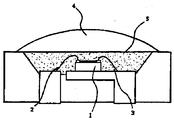
- FIG. 1 is a view showing the structure of a white light emitting diode including a single-phase phosphor according to an embodiment of the present invention
- FIG. 2 shows the emission of a phosphor having a structure of (Gd, Y, Lu, Tb, Ce, Pr, Sm) 3 (Al 1.99 K 0.005 N 0.005 ) [AlO 0.96 F 0.02 N 0.02 ] 3 according to an embodiment of the present invention. Shows the spectrum,
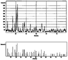
- FIG. 3 is a diagram illustrating an XRD analysis graph of phosphors according to an embodiment of the present invention.
- a white light emitting diode is a nitride semiconductor in which sapphire (Al 2 O 3 ) is formed on a surface thereof, and includes an LED device 1, heterotransition lines 2 and 3, and sapphire.
- substrate 4 and the transparent polymer 5 are included.
- the LED device 1 is implemented with an InGaN-based light emitting diode, and two lines 2 and 3 for hetero transition from the LED device 1 are generated.
- the sapphire substrate 4 is provided on the upper side of the transparent polymer 5 in the shape of a cone packaged with an aluminum polymer, and the transparent polymer 5 is distributed or coated with a phosphor. Description of the phosphor will be described later.
- the white light emitting diode according to the present invention is operated by the form of the fluorescent substance coated transparent polymer 5 and the phosphor, and is fixed to the radiation surface of the hetero transition.
- Application of the hetero phase is named by the fluorescent substance distributed in the transparent polymer 5 and the transparent polymer 5, and particle
- the hetero transition of the LED element 1 is radiated not only on the surface of the sapphire substrate 4 but also on the hetero transition side.
- particles of phosphor are applied to all four sides of the LED element 1 and to the surface substrate of the hetero transition.
- the application method for wavelength conversion is divided into two parts. That is, the circumference
- the thickness of the side of the transparent polymer (5) layer in which the conversion of the wavelength of light occurs and the thickness of the radiating substrate should be the same.
- the thickness of the transparent polymer (5) was adjusted to 80 ⁇ 200 ⁇ m, the optimum thickness was 120 ⁇ 160 ⁇ m. At this time, color change does not occur in all layers, and uniform warm-white light is emitted.
- M molecular weight of the silicone-organic polymer
- the ratio of the phosphor particles and the transparent polymer 5 is also important. If the concentration of the phosphor is lower than 4 ⁇ 5%, the dark blue radiation wavelength is emitted without causing the phosphor particles to emit light. If the particle concentration is 8-9%, the radiation of the original cold light is emitted, and if the concentration is slightly increased, natural and warm colors are emitted.
- the concentration of the phosphor particles was selected as an optimal concentration range of 12 to 16% to increase the luminance and uniformity of the radiation wavelength.
- the phosphor according to the present invention is based on gadolinium (Gd), a rare earth metal ion of garnet type activated with cerium (Ce), and the phosphor element is a substance belonging to groups 1, 3 and 7 of the periodic table and is represented by the following chemical formula. Can be.
- ⁇ Ln Gd, Y, Lu, ⁇ b, Ce, Pr, Sm, and constants A, x, and y are molar ratios, 0.25 ⁇ A ⁇ 3.5, 0.001 ⁇ X ⁇ 0.1, 0.001 ⁇ y ⁇ 0.05.
- Gd is gadolinium
- Y is yttrium
- Lu is lutetium
- ⁇ b is terbium
- Ce cerium
- Pr is praseodymium
- Sm is samarium.
- This long wavelength has two maximum peaks, and the distance between the two peaks is about ⁇ > 25 nm.
- the rare earth metal ions that may be included in the phosphor of the above structure may be used having a concentration range as follows.
- the radiation wavelength emitted from the phosphor changes.
- the concentration of Gd when the concentration of Gd is less than 70%, the position of the short wavelength is shifted, yellow light is emitted, and when 90% is exceeded, the light is reduced.
- the concentration of Y is less than 1%, the light is reduced to emit dark colors, and if it exceeds 2%, yellow light is emitted.
- the concentration of Lu is less than 1%, the light decreases, and if it exceeds 2%, the excitation spectrum of the short wavelength is changed.
- the concentration of Tb is less than 0.01%, the light decreases, and if it exceeds 2%, the light decreases.
- the concentration of Ce is less than 0.1%, the duration of the phosphor increases, and if it exceeds 6.5%, the luminous intensity is lowered.
- the concentration of Sm When the concentration of Sm is less than 0.001%, the brightness decreases, and when it exceeds 0.01%, the brightness of the light decreases. If the concentration of Pr is less than 0.001%, the brightness decreases. If the concentration of Pr exceeds 0.2%, the emission color of the phosphor becomes worse.
- the phosphor when the phosphor is used in the concentration outside the concentration range of the metal ion is used to reduce the light, or to emit a color other than white, it is preferable to implement using a metal having the concentration range. .
- the reason why the sum of the upper limit of the rare earth metal ion exceeds 100% in the composition of the phosphor obtained by using the metal ion is that the initial raw material is volatilized in the process of reducing (nitrogen + hydrogen) at high temperature (about 1000 degrees Celsius) and is lost. (loss) occurs.
- the mixed weight percent exceeds 100%, but this is to compensate for the loss due to volatilization during the chemical reaction, and the composition of the final phosphor is The sum of the above conditions has a composition ratio of not more than 100%.
- each rare earth metal ion has the following characteristics.
- Gd +3 ions together with Ce +3 and Pr +3 form an orange emission wavelength in the radiation phosphor, Y ions shift the radiation wavelength peak in the short wavelength region, and Lu ions shift the radiation wavelength in the short wavelength, To increase the brightness.
- Each particle is in the form of the same compound, creating an immiscible radiation wavelength from fluorescence.
- an irreversible layer is formed on the fluorescent compound, leading to complexity and radiation wavelength infringement in the formation of the phosphor layer.
- the distance ⁇ of the two emission wavelength peaks emitted from the phosphor will depend on the partial equilibrium of the cation lattice of Gd, Y, Lu and Tb.
- the other peak depends on the parity of Gd / Y + Lu + Tb, so that the distance between the spectral peaks by ⁇ / ⁇ + Lu + Tb ( ⁇ ). ) May be changed to 25-50 nm, which may change the color coordinates of the color temperature and radiation wavelength.
- XRD X-ray diffraction
- the phosphor has a garnet structure showing a cubic crystal structure, and the lattice parameter is reduced by a small concentration of F- 1 ions.
- Table 1 is a table showing the wavelength, illuminance, color temperature and color rendering index for each phosphor structure in which the cation lattice structure and the anion lattice structure are changed in the present invention.
Landscapes
- Chemical & Material Sciences (AREA)
- Inorganic Chemistry (AREA)
- Engineering & Computer Science (AREA)
- Materials Engineering (AREA)
- Organic Chemistry (AREA)
- Luminescent Compositions (AREA)
Abstract
본 발명은 단일상 형광체를 포함하는 백색 발광 다이오드에 관한 것이다. 단일상 형광체를 포함하는 백색 발광 다이오드는 세륨(Ce)으로 활성화시킨 석류석 종류의 희토류금속이온 가돌리늄(Gd)을 기초로 한 단일상 화합물인 형광체를 포함하며; 상기 형광체에 포함된 이온은 주기율표의 1. 3. 7족에 속하는 물질로 구현되며, 다음의 화학식으로 표시되는 것을 특징으로 한다. <화학식> (ΣLn)A(Al1-xMeⅠx/2MeⅤx/2)2[AlO4-xFy/2Ny/2]3 상기 화학식에서 ΣLn=Gd, Y, Lu, Тb, Ce, Pr, Sm 이며, 상수 A, x, y는 몰비율(molar ratios)이며, 0.25≤A≤3.5이며, 0.001≤x≤0.1, MeⅠ= Li 또는 Na 또는 K이고, 0.001≤y≤0.05, MeⅤ= V 또는 Nb 또는 Ta이다. 이를 통해, 석류석 희토류 금속이온인 가돌리늄을 기반으로 한 단일상의 형광체를 통해 연색평가지수가 높은 온백색의 빛을 방사할 수 있다.
Description
본 발명은 단일상 형광체를 포함하는 백색 발광 다이오드에 관한 것으로, 구체적으로는 석류석 종류의 희토류 금속 이온인 가돌리늄(Gd)을 기반으로 한 단일상 형광체를 이용하여 온백색을 발광할 수 있는 단일상 형광체를 포함하는 백색 발광 다이오드에 관한 것이다.
최근 발광소자를 사용한 백색 LED가 조명용 백색 광원이나 백라이트 유닛의 백색 광원으로 주목받고 있다.
종래의 백색 LED는 청색, 녹색 및 적색의 3원색 LED를 별도로 구비하여 구현되었으나, 연색성이 부족한 문제가 있었다. 이에, 최근에는 형광체를 이용한 백색 LED가 주로 사용되고 있다.
형광체를 사용하는 백색 LED의 경우, YAG:Ce(yttrium aluminum garnet)형광체가 주로 사용된다. YAG:Ce 형광체를 사용한 백색 LED는 다음과 같은 특징이 있다.
단파장 어두운 청색 빛에 의해 여기(Excitation)되고, 어두운 청색 빛의 고광학적 변환은 노란색으로 발광된다. 그리고, 여기파장의 변수는 YAG:Ce의 농도에 의존하며, 형광체 합성을 위한 원료 물질의 효율성이 높다는 장점을 갖는다.
그러나 YAG:Ce 형광체는 Y3Al5O12 구조의 실용성 즉, 색의 불변성이 떨어진다는 단점이 있다. 그리고, 알려진 형광체들의 표준이 되고 있는 입자 사이즈는 초고온에서만 합성이 가능하며, 형광 여기 파장이 445~465nm로 매우 좁은 스펙트럼 띠를 형성한다는 단점이 있다.
이에 따라 미국특허 US20060169998(A)에서는 terbium-aluminium garnet(ТAG) Tb3Al5O12:Ce를 제안하였다. 이 종래 기술에 따르면 TAG는 λ=425~485nm까지 넓은 여기 스펙트럼을 가지고 있으며, 장파장의 일부는 Ce+3의 이온의 활성화에 의한 형광 물질의 방사파장이 최대 스펙트럼으로서 λ=570nm의 쪽으로 이동하게 된다. 이러한 장파장 이동은 색온도를 Т<4000oК로 낮추게 되고, 초기의 방사파장인 T>6000oК를 T=4000oK로 변경할 수 있어, 사람의 눈에 좀 더 이로운 빛으로 변경이 가능한 장점이 있다.
그러나 TAG를 이용한 형광체는 출발 물질인 산화 텔비움(Тb4O7)이 매우 고가이므로, 상품의 단가가 높아진다는 단점이 있다. 또한 종래의 YAG:Ce를 기반으로 하는 형광체에 비해서도 약 20%정도 밝기가 낮다는 문제점이 있다.
본 발명은 전술한 문제점을 해결하기 위한 것으로, 온백색의 광을 발산하고, 높은 빛 효율을 갖는 단일상 형광체를 포함하는 백색 발광 다이오드를 제공하기 위한 것이다.
또한 본 발명은 축방향의 빛이 1cd 광도의 높은 발광파장을 얻을 수 있는 단일상 형광체를 포함하는 백색 발광 다이오드를 제공하기 위한 것이다.
뿐만 아니라, 본 발명은 연색평가지수가 Ra≥75 이상이며, 비교적 원료비가 저렴한 단일상 형광체를 포함하는 백색 발광 다이오드를 제공하기 위한 것이다.
상기 목적을 달성하기 위하여 본 발명은 단일상 형광체를 포함하는 백색 발광 다이오드에 있어서, 세륨으로 활성화 시킨 석류석 종류의 희토류금속이온 가돌리늄(Gd)을 기초로 한 단일상 화합물인 형광체를 포함하며; 상기 형광체에 포함된 이온은 주기율표의 1. 3. 7족에 속하는 물질로 구현되며, 다음의 화학식으로 표시되는 것을 특징으로 하는 단일상 형광체를 포함하는 백색 발광 다이오드에 의해 달성된다.
<화학식>
(ΣLn)A(Al1-xMeⅠx/2MeⅤx/2)2[AlO4-xFy/2Ny/2]3
상기 화학식에서 ΣLn=Gd, Y, Lu, Тb, Ce, Pr, Sm, Sc 이고, 상수 A, x, y는 몰비율(molar ratios)이며, 0.25≤A≤3.5이고, 0.001≤x≤0.1, MeⅠ= Li 또는 Na 또는 K이며, 0.001≤y≤0.05, MeⅤ= V 또는 Nb 또는 Ta이다.
상기 화학식을 가지는 형광체에는 희토류 금속이온의 농도가 70%<Gd≤90%, 1%<Y≤2%, 1%<Lu≤2%, 0.01%≤Tb≤2%, 0.1%<Ce≤6.5%, 0.001%<Sm≤0.01%, 0.001%<Pr≤0.2%에 해당하는 희토류 금속 중에서 Gd, Y, Lu 금속을 기반으로 Tb, Ce, Pr, Sm 중 적어도 하나의 희토류 금속을 첨가하여 형성하도록 한다.
그리고 λ=430~480nm에 의해 여기하고 여기파장에 의해 넓은 범위의 장파장 λ=610±2nm의 발광파장을 갖게 되며, 상기 장파장은 적어도 2개의 최대 피크를 가지며, 상기 최대 피크 간의 거리는 약 Δλ> 25nm인 것이 바람직하다.
상기 형광체에 포함된 사면체 구조의 AlO4에서 산소 O-2의 이온을 F-1 또는 N-3와 치환시켜, 복사파장의 세기를 증가시킬 수 있다.
상기 형광체 입자의 형태는 사각형의 팔면체 구조로 중 직경이 d50=2~4μm이고, 변수 d90≤20μm인 것이 바람직하다.
상기 형광체는 활성화 이온으로 Ce+3, Pr+3, Sm+3 중 적어도 하나를 첨가하며, 상기 첨가된 활성화 이온은 각각 다른 복사파장을 형성할 수 있다.
상기 Ce+3를 첨가하여 d-f 오비탈의 전자전이를 보충하며, 상기 Ce+3 및 Pr+3를 첨가하여 상기 복사파장의 최대 장파장의 세기가 증가되며, 상기 Ce+3, Pr+3 및 Sm+3을 첨가하여 상기 복사파장의 스펙트럼 띠가 λ=620~630nm으로 형성되는 것이 바람직하다.
상기 형광체의 기초 형광물질은 Y+Lu+Tb/Gd이며, 상기 기초 형광물질에 5족 원소 Nb, Ta를 첨가하여 스펙트럼의 반치폭(half width at half maximum)을 증가시킬 수 있다.
상기 기초 형광물질에 1족의 Li, Na, K 이온 중 적어도 하나의 이온을 혼합하여 스펙트럼의 반치폭을 증가시키는 것이 바람직하다.
상기 형광체가 도포된 투명 고분자를 더 포함하고; 상기 투명 고분자는 실리콘 그룹인 Si-O-C-C-O-Si 와 분자량 M=150000~250000의 카본 유닛의 실리콘 유기 고분자를 포함할 수 있다.
상기 투명 고분자에 분포된 형광체 입자는 질량농도가 6% 내지 18%로 분산된 고분자와의 결합에 의해 빛을 재방사(reradiationg)할 수 있고, 상기 투명 고분자의 측면 및 방사기판은 동일한 두께를 갖는 것이 바람직하다.
상기 형광체와 상기 투명 고분자 사이의 굴절지수의 비율은 1.85:1.55일 수 있고, 상기 백색 발광 다이오드의 색온도는 Т≤4000~3000°К인 온백색의 복사파장을 가지며, 상기 백색 발광 다이오드의 연색평가지수(color randering index)는 75<Ra≤86인 것이 바람직하다.
상기 투명 고분자의 축방향의 광도는 20~35cd이고, 복사파장 공경(aperture)의 반각(half-angle)은 2Θ=120 °인 것이 바람직하다.
상기 백색 발광 다이오드에 인가되는 직류전압이 i=50~350mA인 경우 광효율η=115~95lm/W이며, 상기 직류전압이 i=200~400mA이면, 연색평가지수가 81 이상으로 증가할 수 있다.
상기 복사파장의 피크(peak)의 이동(shift)에 의해 상기 연색평가지수가 증가되어 상기 복사파장의 장파장 Δλ=5~10nm인 것이 바람직하고, 상기 복사파장의 색좌표의 합은 ΣX+Y≤0.85이며, X좌표와 Y좌표가 인접해 있을 수 있다.
따라서 본 발명은 석류석 희토류 금속이온인 가돌리늄을 기반으로 한 단일상의 형광체를 통해 연색평가지수가 높은 온백색의 빛을 방사할 수 있어, 여러 가지 색을 혼합할 필요가 없으며, 화학성분이 균일한 단일상 형광체를 포함하는 백색 발광 다이오드가 제공된다.
또한 본 발명은 단일상 형광체를 이용하여 균일한 온백색의 빛을 방사할 수 있어 제조비가 비교적 저렴한 단일상 형광체를 포함하는 백색 발광 다이오드가 제공된다.
또한 본 발명은 헤테로전이에 공급 전류가 증가하면 광속도 및 광효율이 높아지므로, 종래의 발광 램프와 비교하여 경제적 효과가 있는 단일상 형광체를 포함하는 백색 발광 다이오드가 제공된다.
도 1은 본 발명의 일실시예에 따른 단일상 형광체를 포함하는 백색 발광 다이오드의 구조를 도시한 도면이고,
도 2는 본 발명의 일실시예에 따른 (Gd, Y, Lu, Tb, Ce, Pr, Sm)3(Al1.99K0.005N0.005)[AlO0.96F0.02N0.02]3 구조를 갖는 형광체의 방사 스펙트럼을 도시한 도면이며,
도 3은 본 발명의 일실시예에 따른 형광체에 대한 XRD 분석 그래프를 도시한 도면이다.
이하, 첨부한 도면을 참조하여 본 발명의 바람직한 실시예에 대해 설명하기로 한다.
도 1은 본 발명의 일실시예에 따른 단일상 형광체를 포함하는 백색 발광 다이오드의 구조를 도시한 도면이다. 도 1을 참조하면, 본 실시예에 따른 백색 발광 다이오드는 표면에 사파이어(Al2O3)가 형성되는 질화물 반도체이며, LED 소자(1)와, 헤테로전이용 선(2, 3)과, 사파이어 기판(4)과, 투명 고분자(5)를 포함한다.
본 실시예에 따른 LED 소자(1)는 InGaN계의 발광 다이오드로 구현되며, LED 소자(1)로부터의 헤테로전이를 위한 두개의 선(2, 3)이 생성된다.
사파이어 기판(4)은 알루미늄 폴리머로 패키징된 원추모양으로 투명 고분자(5) 상측에 마련되며, 투명 고분자(5)는 형광체가 분포 또는 도포된다. 형광체에 대한 설명은 후술하기로 한다.
본 발명에 따른 백색 발광 다이오드는 헤테로 상의 도포된 투명 고분자(5)와 형광체의 형태에 의해 동작되며, 헤테로 전이의 방사표면에 고정된다. 헤테로 상의 도포는 투명 고분자(5)와 투명 고분자(5)에 분포된 형광체에 의해 이름이 붙여지고, 형광체의 입자가 분포된다.
LED 소자(1)의 헤테로 전이는 사파이어 기판(4)의 표면뿐만 아니라 헤테로 전이 측면에서도 방사된다. 따라서 형광체의 입자를 LED 소자(1)의 모든 4개의 측면과 헤테로 전이의 표면 기판에 도포한다. 파장 변환을 위한 도포 방법은 두 부분으로 나뉜다. 즉, LED 측면의 표면을 제외한 LED 소자(1) 주위(옆부분)는 근접해서 도포하고, 빛을 발하는 표면은 형광체로 도포한다.
빛의 파장의 변환이 일어나는 투명 고분자(5) 층의 측면과 방사기판의 두께는 같아야 한다. 본 실시예에서는 투명 고분자(5)의 두께를 80~200μm까지 조절하였으며, 최적의 두께는 120~160μm이었다. 이때, 모든 층에서 색의 변경이 발생하지 않고, 균일한 온백색(warm-white)의 빛이 방사된다.
그리고 투명 고분자(5)의 축방향의 광도는 20~35cd이고, 방사파장 공경(aperture)의 반각(half-angle), 즉 투명 고분자(5)의 방사각도는 2Θ=120 °이다.
투명 고분자(5)는 실리콘 그룹인 Si-O-C-C-O-와 분자량 M=15000~25000의 탄소 유닛의 실리콘-유기 고분자(silicon-organic polymer)를 함유하는 구조로 형성된다. 실리콘-유기 고분자의 분자량이 높으면, 점성이 높아진다. 따라서, 실리콘-유기 고분자의 분자량을 조절하여, 빛의 파장의 변환이 일어나는 투명 고분자(5)의 층 두께를 조작할 수 있다.
형광체와 실리콘-유기 고분자 사이의 굴절 지수의 비율은 1.85 : 1.55가 되어야 한다. 기술된 형광체의 굴절 지수 n=1.85인데 반해, 실리콘-유기 고분자의 굴절지수는 1.55에서 1.65까지 변한다. 고분자의 굴절 지수 증가는 형광체 입자의 방사파장 각도를 증가시키는 원인이 되어, 백색 LED의 발광의 휘도의 증가를 돕는다.
형광체 입자와 투명 고분자(5)의 비율도 중요하다. 만약 형광체의 농도가 4~5% 미만으로 낮으면 어두운 파란색의 방사파장이 형광체 입자의 발광 현상을 일으키지 않고 빠져나가게 된다. 입자 농도가 8~9%가 된다면 원래의 냉광(cold light)의 방사파장이 방사되고, 농도를 약간 더 증가시키면 자연스럽고 따듯한 색이 방사된다.
형광체 입자의 농도가 15~16%이면, 강한 세기의 온백색(색온도 T=4000~3000oК)을 방사한다. 형광체 입자의 농도를 20%이상 증가시키면 백색이 감소하는 어두운 파란색 빛이 방사된다. 이 방사파장으로 노란색, 오렌지색, 빨간색의 구현이 가능하다.
본 실시예에서는 형광체 입자의 농도를 휘도와 방사파장의 균일성을 높이는 12~16%를 최적의 농도범위로 선택하였다.
본 발명에 따른 형광체는 세륨(Ce)으로 활성화시킨 석류석 종류의 희토류 금속이온인 가돌리늄(Gd)을 기초로 하며, 형광물질 요소는 주기율표의 1, 3, 7족에 속하는 물질로 다음의 화학식으로 나타낼 수 있다.
[화학식]
(ΣLn)A(Al1-xMeⅠx/2MeⅤx/2)2[AlO4-xFy/2Ny/2]3
상기 식에서 ΣLn=Gd, Y, Lu, Тb, Ce, Pr, Sm 이며, 상수 A, x, y는 몰비율(molar ratios)이고, 0.25≤A≤3.5 이며, 0.001≤X≤0.1, 0.001≤y≤0.05이다. 그리고 MeⅠ= Li 또는 Na 또는 K이고, MeⅤ= Nb 또는 Ta이다.
상기 Ln에 포함되는 희토류 금속에서 Gd는 가돌리늄, Y는 이트륨, Lu는 루테튬, Тb는 테르븀, Ce는 세륨, Pr은 프라세오디뮴, Sm은 사마륨이다.
본 실시예에 따른 형광체는 짧은 파장 λ=430~480nm에 의해 여기(exciation)되고, 여기파장에 의해 넓은 범위의 장파장 λ=610±2nm의 발광파장을 갖게 된다. 이 장파장은 최대 피크가 2개가 형성되며, 이 2개의 피크 간의 거리는 약 Δλ>25nm이다.
상기 화학식을 구조의 형광체에 포함될 수 있는 희토류 금속이온은 다음과 같은 농도범위를 가지는 것을 사용하도록 한다.
70%<Gd≤90%, 1%<Y≤2%, 1%<Lu≤2%, 0.01%≤Tb≤2%, 0.1%<Ce≤6.5%, 0.001%<Sm≤0.01%, 0.001%<Pr≤0.2%(여기서, 농도는 중량%이다)에 해당하는 희토류 금속 중에서 Gd, Y, Lu 금속을 기반으로 Tb, Ce, Pr, Sm 중 적어도 하나의 희토류 금속을 첨가하여 형성하도록 한다.
상기 희토류 금속이온의 농도는 각각의 임계치에 미달되거나 초과하여 포함되면 형광체로부터 방출되는 방사파장이 변화하게 된다.
즉, Gd의 농도가 70% 미만이면 짧은 파장의 위치가 이동하고, 노란색 빛이 방사되며, 90%가 초과되면 빛이 감소된다. Y의 농도가 1% 미만이면 빛이 감소하여 어두운 색이 방사되고, 2%를 초과하면 노란색 빛이 방사된다. Lu의 농도가 1% 미만이면 빛이 감소하고, 2%를 초과하면 짧은 파장의 여자 스펙트럼이 변경된다. Tb의 농도가 0.01% 미만이면 빛이 감소하고, 2%를 초과한 경우에도 빛이 감소한다. Ce의 농도가 0.1% 미만이면 형광체의 지속시간이 증가하며, 6.5%를 초과하면 광도가 떨어진다. Sm의 농도가 0.001% 미만이면 밝기가 감소하고, 0.01%를 초과한 경우에도 빛의 밝기가 감소한다. Pr의 농도가 0.001% 미만이면 밝기가 감소하고, 0.2%를 초과하면 형광체의 방출색이 나빠진다.
따라서 상기 형광체를 형성함에 있어 상기 금속이온의 농도 범위를 벗어난 것을 사용하게 되면 빛이 감소하거나, 흰색이 아닌 다른 색이 방사되게 되므로, 반드시 상기 농도의 범위를 가지는 금속을 이용하여 구현하는 것이 바람직하다.
여기서 상기 금속이온을 이용하여 얻어진 형광체의 조성에 희토류 금속이온의 상한치의 합이 100%가 초과되는 이유는, 최초 원료 물질이 고온(약 천도)에서 환원(질소+수소)되는 과정에서 휘발되어 손실(loss)이 발생하기 때문이다. 예컨대, Gd, Lu, Tb, Ce 등 4가지의 원소를 사용하여 형광체를 형성할 경우, 그 농도의 합은 90+3+2+6.5=101.5%가 되지만, 손실로 인해 최종에는 약 100%가 되는 것이다.
다시 말해, 원료 희토류 금속의 중량%를 전술한 농도의 조건과 같이 혼합하면, 혼합된 중량%가 100%를 초과되지만 이는 화학반응시 휘발로 인한 손실을 보정하기 위해 것이며, 최종의 형광체의 조성은 상기 조건 중 총합이 100%가 넘지 않는 조성비를 갖게 된다.
각 희토류 금속이온의 양이온 격자 구조는 유사하며, 각 성분은 다음과 같은 특성을 갖는다.
Gd+3 이온은 Ce+3, Pr+3와 함께 방사파장 형광체에 오렌지색 방사파장을 형성시키며, Y 이온은 단파장 부분의 방사파장 피크를 이동시키고, Lu 이온은 단파장의 방사파장을 이동시키고, 발광의 밝기를 증가시킨다.
Tb 이온은 형광체의 여기파장 스펙트럼 띠를 λ=430nm로 확장 시키며, Ce+3 이온은 방사파장의 기본 스펙트럼 피크를 λ=582 nm~548 nm으로 형성시킨다. Pr+3 이온은 두 번째 피크를 λмах=610±2nm 로 형성 시키며, Sm+3 이온은 기본 스펙트럼 곡선의 방사파장 반치폭을 확장시킨다.
그리고 각각의 입자가 동일한 화합물의 형태를 하고 있어, 형광으로부터의 혼합되지 않는 복사파장을 만든다. 높은 재생산성을 위해 2가 또는 3가 화합물을 혼합함으로써, 형광 화합물에 비가역적 층을 형성시키고, 형광체 층의 형성에 복합성과 방사파장 색의 침해를 이끌어낸다.
또한 형광체의 대부분의 입자는 입자 간 접착력이 낮아 입자가 뭉쳐 있지 않으며, 이러한 입자 구조는 철저한 분산 또는 일반적인 분산의 재현성이 좋아 중간 분산에 용이하다.
형광체로부터 방사되는 2개의 방사파장 스펙트럼 피크의 거리(Δλ)는 Gd, Y, Lu 그리고 Tb의 양이온 격자의 부분적 평형에 의존하게 된다. 다시 말해, 한 개의 피크는 λ=610±2nm이고, 다른 한 개의 피크는 Gd/Y+Lu+Tb의 평형(parity)에 의존하므로, Gd/Y+Lu+Tb에 의해 스펙트럼 피크 간의 거리(Δλ)가 25~50nm로 변경될 수 있고, 이 때문에 색온도와 방사파장의 색좌표가 변경될 수 있다. 이에 λ=626~630nm의 제3의 스펙트럼 곁가지 피크를 교정할 수 있게 된다.
또한 석류석의 구조는 입방체 결정격자이므로, 결정격자의 격자 변수(a)가 Lu+Tb+Y/Gd의 평형의 변화에 따라 변화되는 a=12.0±0.1값을 갖는다.
도 3은 본 발명에 따른 형광체를 “Dron-2” 장치로 Ua=40kE-v에서 XRD(X-ray Dirreaction) 분석한 결과이다. 도 3을 참조하면, 형광체는 석류석 구조로 입방체 결정구조를 나타내고 있고, 이 격자의 변수는 F-1이온의 적은 농도에 의해 감소한다. 그러나 모든 시료의 결정격자의 변수 크기에 대해서는 근본적으로 а=12.05±0.05으로 동일하다.
본 실시예에 따른 형광체는 Gd/Y+Lu+Tb에 5족 원소 Nb, Ta가 별도로 첨가되면, 기본 스펙트럼의 최대 방사파장이 Δλ=2~4nm만큼 반치폭이 증가된다.
표 1은 본 발명에서 양이온 격자 구조와 음이온 격자 구조를 변화시킨 각 형광체 구조별 실시예에 대한 파장, 조도, 색 온도 및 연색평가지수를 나타낸 표이다.
표 1
| 양이온 격자 구조 | 음이온 격자 구조 | 파장(최대,nm) | 조도 | 색온도 | 연색평가지수 Ra |
| Gd,Y,Lu,Tb,Ce,Pr,Sm)3 | (Al1.98Li0.01V0.01)[AlO0.99F0.01N0.01]3 | 609.2585 | 17677 | 3275 | 74.3 |
| (Gd,Y,Lu,Tb,Ce,Pr,Sm)3 | (Al1.98Na0.01Nb0.01)[AlO0.98F0.01N0.01]3 | 609.1587 | 21139 | 3409 | 75.4 |
| (Gd,Y,Lu,Tb,Ce,Pr,Sm)3 | (Al1.96Li0.02Ta0.02)[AlO0.96F0.02N0.02]3 | 609.2583 | 17931 | 3441 | 76.2 |
| (Gd,Y,Lu,Tb,Ce,Pr,Sm)3 | (Al1.99K0.005N0.005)[AlO0.96F0.02N0.02]3 | 609.1586 | 18608 | 3541 | 78.1 |
| (Gd,Lu,Tb,Ce,Pr,Sm)3 | (Al1.94Li0.03Ta0.03)[AlO0.98F0.01N0.01]3 | 609.1587 | 20005 | 3600 | 80.1 |
Claims (13)
- 단일상 형광체를 포함하는 백색 발광 다이오드에 있어서,세륨(Ce)으로 활성화시킨 석류석 종류의 희토류금속이온 가돌리늄(Gd)을 기초로 한 단일상 화합물인 형광체를 포함하며,상기 형광체에 포함된 이온은 주기율표의 1. 3. 7족에 속하는 물질로 구현되며, 다음의 화학식으로 표시되는 것을 특징으로 하는 단일상 형광체를 포함하는 백색 발광 다이오드.<화학식>(ΣLn)A(Al1-xMeⅠx/2MeⅤx/2)2[AlO4-yFy/2Ny/2]3상기 화학식에서 ΣLn=Gd, Y, Lu, Тb, Ce, Sm, Pr 이고, 상수 A, x, y는 몰비율(molar ratios)이며, 0.25≤A≤3.5이고, 0.001≤X≤0.1, MeⅠ= Li 또는 Na 또는 K이며, 0.001≤y≤0.05, MeⅤ= V 또는 Nb 또는 Ta이다.
- 제1항에 있어서,상기 형광체에 포함되는 희토류 금속은 그 농도가 70%<Gd≤90%, 1%<Y≤2%, 1%<Lu≤2%, 0.01%≤Tb≤2%, 0.1%<Ce≤6.5%, 0.001%<Sm≤0.01%, 0.001%<Pr≤0.2% 인 것을 특징으로 하는 단일상 형광체를 포함하는 백색 발광 다이오드.
- 제2항에 있어서,상기 형광체는 단파장과 장파장이 발생하며, 상기 단파장에 의한 여기파장에 의해 상기 장파장이 발생하며, 상기 장파장은 적어도 2개의 최대 피크를 가지며, 상기 최대 피크 간의 거리는 Δλ> 25nm인 것을 특징으로 하는 단일상 형광체를 포함하는 백색 발광 다이오드.
- 제3항에 있어서,상기 형광체에 포함된 사면체 구조의 AlO4에서 산소 O-2의 이온을 F-1또는 N-3와 치환시켜, 복사파장의 세기를 증가시키는 것을 특징으로 하는 단일상 형광체를 포함하는 백색 발광 다이오드.
- 제4항에 있어서,상기 형광체 입자의 형태는 사각형의 팔면체 구조로 중 직경이 d50=2~4μm이고, 변수 d90≤20μm인 것을 특징으로 하는 단일상 형광체를 포함하는 백색 발광 다이오드.
- 제5항에 있어서,상기 형광체는 활성화 이온으로 Ce+3, Pr+3, Sm+3 중 적어도 하나를 첨가하며, 상기 Ce+3를 첨가하여 d-f 오비탈의 전자 전이를 보충하고, 상기 Ce+3 및 Pr+3를 첨가하여 상기 복사파장의 최대 장파장의 세기를 증가시키고, 상기 Ce+3, Pr+3 및 Sm+3을 첨가하여 상기 복사파장의 스펙트럼 띠가 λ=620~630nm으로 형성되도록 하는 것을 특징으로 하는 단일상 형광체를 포함하는 백색 발광 다이오드.
- 제6항에 있어서,상기 형광체의 기초 형광물질은 Y+Lu+Tb/Gd이며, 상기 기초 형광물질에 5족 원소 Nb, Ta 또는 1족의 Li, Na, K 이온 중 적어도 하나의 이온을 혼합하여 스펙트럼의 반치폭을 증가시키는 것을 특징으로 하는 단일상 형광체를 포함하는 백색 발광 다이오드.
- 제1항 내지 제7항 중 어느 한 항에 있어서,상기 형광체가 도포된 투명 고분자를 더 포함하고,상기 투명 고분자의 측면 및 방사기판은 동일한 두께를 가지며, 상기 투명 고분자의 축방향의 광도는 20~35cd이고, 복사파장 공경(aperture)의 반각(half-angle)은 2Θ=120 °이며, 상기 형광체와 상기 투명 고분자 사이의 굴절지수의 비율은 1.85:1.55인 것을 특징으로 하는 단일상 형광체를 포함하는 백색 발광 다이오드
- 제8항에 있어서,상기 투명 고분자는 실리콘 그룹인 Si-O-C-C-O-Si 와 분자량 M=150000~250000의 카본 유닛의 실리콘 유기 고분자를 포함하며, 상기 투명 고분자에 분포된 형광체 입자는 질량농도가 6%~18%로 분산된 고분자와의 결합에 의해 빛을 재방사하는 것을 특징으로 하는 단일상 형광체를 포함하는 백색 발광 다이오드.
- 제9항에 있어서,상기 백색 발광 다이오드의 연색평가지수는 75<Ra≤86인 것을 특징으로 하는 단일상 형광체를 포함하는 백색 발광 다이오드.
- 제10항에 있어서,상기 백색 발광 다이오드에 인가되는 직류전압이 i=50~350mA인 경우 광효율η=115~95lm/W이며, 상기 직류전압이 i=200~400mA이면 연색평가지수가 81 이상으로증가하는 것을 특징으로 하는 단일상 형광체를 포함하는 백색 발광 다이오드.
- 제11항에 있어서,상기 복사파장의 피크(peak)의 이동(shift)에 의해 상기 연색평가지수가 증가되어 상기 복사파장의 장파장의 최대 피크 간의 거리가 증가하는 것을 특징으로 하는 단일상 형광체를 포함하는 백색 발광 다이오드.
- 제12항에 있어서,상기 복사파장의 색좌표의 합은 ΣX+Y≤0.85이며, X좌표와 Y좌표가 인접해 있는 것을 특징으로 하는 단일상 형광체를 포함하는 백색 발광 다이오드.
Applications Claiming Priority (2)
| Application Number | Priority Date | Filing Date | Title |
|---|---|---|---|
| KR10-2011-0036498 | 2011-04-20 | ||
| KR1020110036498A KR101337999B1 (ko) | 2011-04-20 | 2011-04-20 | 단일상 형광체를 포함하는 백색 발광 다이오드 |
Publications (1)
| Publication Number | Publication Date |
|---|---|
| WO2012144686A1 true WO2012144686A1 (ko) | 2012-10-26 |
Family
ID=47041765
Family Applications (1)
| Application Number | Title | Priority Date | Filing Date |
|---|---|---|---|
| PCT/KR2011/003675 Ceased WO2012144686A1 (ko) | 2011-04-20 | 2011-05-18 | 단일상 형광체를 포함하는 백색 발광 다이오드 |
Country Status (2)
| Country | Link |
|---|---|
| KR (1) | KR101337999B1 (ko) |
| WO (1) | WO2012144686A1 (ko) |
Families Citing this family (1)
| Publication number | Priority date | Publication date | Assignee | Title |
|---|---|---|---|---|
| RU2619318C2 (ru) * | 2015-08-17 | 2017-05-15 | Акционерное общество "Научно-исследовательский институт "Платан" с заводом при НИИ" | Фотолюминофор нейтрально-белого цвета свечения со структурой граната и светодиод на его основе |
Citations (5)
| Publication number | Priority date | Publication date | Assignee | Title |
|---|---|---|---|---|
| EP1429397A2 (en) * | 1996-07-29 | 2004-06-16 | Nichia Chemical Industries, Ltd. | Light emitting device |
| US20090105065A1 (en) * | 2006-03-23 | 2009-04-23 | Koninklijke Philips Electronics N.V. | Light emitting device with a ceramic garnet material |
| US20090289545A1 (en) * | 2008-05-26 | 2009-11-26 | Soshchin Naum | Warm-White Light-Emitting Diode and Its Phosphor Powder |
| US20090315449A1 (en) * | 2008-06-20 | 2009-12-24 | Soshchin Naum | Warm-white light-emitting diode and its orange phosphor powder |
| US20100044729A1 (en) * | 2008-08-22 | 2010-02-25 | Soshchin Naum | Warm-white light emtitting diode and its halide phosphor powder |
Family Cites Families (1)
| Publication number | Priority date | Publication date | Assignee | Title |
|---|---|---|---|---|
| US7094362B2 (en) * | 2003-10-29 | 2006-08-22 | General Electric Company | Garnet phosphor materials having enhanced spectral characteristics |
-
2011
- 2011-04-20 KR KR1020110036498A patent/KR101337999B1/ko not_active Expired - Fee Related
- 2011-05-18 WO PCT/KR2011/003675 patent/WO2012144686A1/ko not_active Ceased
Patent Citations (5)
| Publication number | Priority date | Publication date | Assignee | Title |
|---|---|---|---|---|
| EP1429397A2 (en) * | 1996-07-29 | 2004-06-16 | Nichia Chemical Industries, Ltd. | Light emitting device |
| US20090105065A1 (en) * | 2006-03-23 | 2009-04-23 | Koninklijke Philips Electronics N.V. | Light emitting device with a ceramic garnet material |
| US20090289545A1 (en) * | 2008-05-26 | 2009-11-26 | Soshchin Naum | Warm-White Light-Emitting Diode and Its Phosphor Powder |
| US20090315449A1 (en) * | 2008-06-20 | 2009-12-24 | Soshchin Naum | Warm-white light-emitting diode and its orange phosphor powder |
| US20100044729A1 (en) * | 2008-08-22 | 2010-02-25 | Soshchin Naum | Warm-white light emtitting diode and its halide phosphor powder |
Also Published As
| Publication number | Publication date |
|---|---|
| KR101337999B1 (ko) | 2013-12-06 |
| KR20120118873A (ko) | 2012-10-30 |
Similar Documents
| Publication | Publication Date | Title |
|---|---|---|
| Wang et al. | Highly efficient narrow-band green and red phosphors enabling wider color-gamut LED backlight for more brilliant displays | |
| Oh et al. | Analysis of wide color gamut of green/red bilayered freestanding phosphor film-capped white LEDs for LCD backlight | |
| CN108291141B (zh) | 窄带红色磷光体 | |
| US9507200B2 (en) | Method of manufacturing image display device and method of selecting color filter | |
| TWI690750B (zh) | 量子點顯示裝置 | |
| WO2014117400A1 (zh) | 背光模组及液晶显示装置 | |
| US9657222B2 (en) | Silicate phosphors | |
| JP2008517091A (ja) | 蛍光体及びその蛍光体を利用した発光素子{Phosphorandlightemittingdeviceusingthesame} | |
| WO2013115542A1 (ko) | 광산란을 최소화하는 형광체-기지 복합체 분말 및 이를 포함하는 led 구조체 | |
| CN110534631B (zh) | 一种led结合钙钛矿量子点微晶玻璃的显示用宽色域背光源 | |
| US7919785B2 (en) | Phosphor for white light-emitting diodes and fabrication of the same | |
| CN102994079A (zh) | 氮氧化物橙-红色荧光物质,包括其的发光膜或发光片及发光器件 | |
| WO2013015597A2 (ko) | 백색 led 장치 | |
| CN1547266A (zh) | 以二次激光方式产生白光光源的方法及其白光发光组件 | |
| Liu et al. | Phosphor Handbook: Novel Phosphors, Synthesis, and Applications | |
| KR20220088454A (ko) | 고색 영역 포토루미네선스 파장 변환된 백색 발광 디바이스 | |
| JP2008235458A (ja) | 白色発光装置、これを用いてなるバックライトおよび表示装置並びに照明装置 | |
| CN103045257B (zh) | 一种氮化物发光材料及采用该发光材料制成的发光器件 | |
| TWI551667B (zh) | 碳二亞胺磷光體 | |
| US20070090327A1 (en) | Novel red fluorescent powder | |
| EP1803162B1 (en) | Phosphor, light emitting device by using the same and manufacturing method of the same | |
| WO2012144686A1 (ko) | 단일상 형광체를 포함하는 백색 발광 다이오드 | |
| WO2010016740A2 (en) | Red phosphor and forming method thereof for use in solid state lighting | |
| KR101017136B1 (ko) | 신규 형광체 및 이의 제조 | |
| TWI266563B (en) | Compound, phosphor composition and light-emitting device containing the same |
Legal Events
| Date | Code | Title | Description |
|---|---|---|---|
| 121 | Ep: the epo has been informed by wipo that ep was designated in this application |
Ref document number: 11863819 Country of ref document: EP Kind code of ref document: A1 |
|
| NENP | Non-entry into the national phase |
Ref country code: DE |
|
| 122 | Ep: pct application non-entry in european phase |
Ref document number: 11863819 Country of ref document: EP Kind code of ref document: A1 |