WO2012147341A1 - 磁性シートとそれを用いた非接触受電装置、電子機器および非接触充電装置 - Google Patents
磁性シートとそれを用いた非接触受電装置、電子機器および非接触充電装置 Download PDFInfo
- Publication number
- WO2012147341A1 WO2012147341A1 PCT/JP2012/002818 JP2012002818W WO2012147341A1 WO 2012147341 A1 WO2012147341 A1 WO 2012147341A1 JP 2012002818 W JP2012002818 W JP 2012002818W WO 2012147341 A1 WO2012147341 A1 WO 2012147341A1
- Authority
- WO
- WIPO (PCT)
- Prior art keywords
- magnetic
- magnetic sheet
- ribbon
- power receiving
- coil
- Prior art date
- Legal status (The legal status is an assumption and is not a legal conclusion. Google has not performed a legal analysis and makes no representation as to the accuracy of the status listed.)
- Ceased
Links
Images


Classifications
-
- H—ELECTRICITY
- H01—ELECTRIC ELEMENTS
- H01F—MAGNETS; INDUCTANCES; TRANSFORMERS; SELECTION OF MATERIALS FOR THEIR MAGNETIC PROPERTIES
- H01F1/00—Magnets or magnetic bodies characterised by the magnetic materials therefor; Selection of materials for their magnetic properties
- H01F1/01—Magnets or magnetic bodies characterised by the magnetic materials therefor; Selection of materials for their magnetic properties of inorganic materials
- H01F1/03—Magnets or magnetic bodies characterised by the magnetic materials therefor; Selection of materials for their magnetic properties of inorganic materials characterised by their coercivity
- H01F1/12—Magnets or magnetic bodies characterised by the magnetic materials therefor; Selection of materials for their magnetic properties of inorganic materials characterised by their coercivity of soft-magnetic materials
- H01F1/14—Magnets or magnetic bodies characterised by the magnetic materials therefor; Selection of materials for their magnetic properties of inorganic materials characterised by their coercivity of soft-magnetic materials metals or alloys
- H01F1/147—Alloys characterised by their composition
- H01F1/153—Amorphous metallic alloys, e.g. glassy metals
- H01F1/15308—Amorphous metallic alloys, e.g. glassy metals based on Fe/Ni
-
- H—ELECTRICITY
- H01—ELECTRIC ELEMENTS
- H01F—MAGNETS; INDUCTANCES; TRANSFORMERS; SELECTION OF MATERIALS FOR THEIR MAGNETIC PROPERTIES
- H01F27/00—Details of transformers or inductances, in general
- H01F27/34—Special means for preventing or reducing unwanted electric or magnetic effects, e.g. no-load losses, reactive currents, harmonics, oscillations, leakage fields
- H01F27/36—Electric or magnetic shields or screens
- H01F27/366—Electric or magnetic shields or screens made of ferromagnetic material
-
- H—ELECTRICITY
- H01—ELECTRIC ELEMENTS
- H01F—MAGNETS; INDUCTANCES; TRANSFORMERS; SELECTION OF MATERIALS FOR THEIR MAGNETIC PROPERTIES
- H01F38/00—Adaptations of transformers or inductances for specific applications or functions
- H01F38/14—Inductive couplings
-
- H—ELECTRICITY
- H02—GENERATION; CONVERSION OR DISTRIBUTION OF ELECTRIC POWER
- H02J—ELECTRIC POWER NETWORKS; CIRCUIT ARRANGEMENTS OR SYSTEMS FOR SUPPLYING OR DISTRIBUTING ELECTRIC POWER; SYSTEMS FOR STORING ELECTRIC ENERGY
- H02J50/00—Circuit arrangements or systems for wireless supply or distribution of electric power
- H02J50/10—Circuit arrangements or systems for wireless supply or distribution of electric power using inductive coupling
- H02J50/12—Circuit arrangements or systems for wireless supply or distribution of electric power using inductive coupling of the resonant type
-
- H—ELECTRICITY
- H02—GENERATION; CONVERSION OR DISTRIBUTION OF ELECTRIC POWER
- H02J—ELECTRIC POWER NETWORKS; CIRCUIT ARRANGEMENTS OR SYSTEMS FOR SUPPLYING OR DISTRIBUTING ELECTRIC POWER; SYSTEMS FOR STORING ELECTRIC ENERGY
- H02J50/00—Circuit arrangements or systems for wireless supply or distribution of electric power
- H02J50/70—Circuit arrangements or systems for wireless supply or distribution of electric power involving the reduction of electric, magnetic or electromagnetic leakage fields
-
- H—ELECTRICITY
- H02—GENERATION; CONVERSION OR DISTRIBUTION OF ELECTRIC POWER
- H02J—ELECTRIC POWER NETWORKS; CIRCUIT ARRANGEMENTS OR SYSTEMS FOR SUPPLYING OR DISTRIBUTING ELECTRIC POWER; SYSTEMS FOR STORING ELECTRIC ENERGY
- H02J50/00—Circuit arrangements or systems for wireless supply or distribution of electric power
- H02J50/90—Circuit arrangements or systems for wireless supply or distribution of electric power involving detection or optimisation of position, e.g. alignment
-
- H—ELECTRICITY
- H02—GENERATION; CONVERSION OR DISTRIBUTION OF ELECTRIC POWER
- H02J—ELECTRIC POWER NETWORKS; CIRCUIT ARRANGEMENTS OR SYSTEMS FOR SUPPLYING OR DISTRIBUTING ELECTRIC POWER; SYSTEMS FOR STORING ELECTRIC ENERGY
- H02J7/00—Circuit arrangements for charging or discharging batteries or for supplying loads from batteries
- H02J7/60—Circuit arrangements for charging or discharging batteries or for supplying loads from batteries including safety or protection arrangements
- H02J7/61—Circuit arrangements for charging or discharging batteries or for supplying loads from batteries including safety or protection arrangements against overcharge
Definitions
- Embodiments of the present invention relate to a magnetic sheet and a non-contact power receiving device, an electronic device, and a non-contact charging device using the magnetic sheet.
- contact charging charging is performed by directly contacting the electrode of the power receiving device and the electrode of the power feeding device.
- the contact charging method is generally used because of its simple device structure.
- the weight of electronic devices has been reduced, and the contact pressure between the electrode of the power receiving device and the electrode of the power feeding device has become insufficient, resulting in a problem of charging failure.
- the secondary battery is vulnerable to heat, it is necessary to design a circuit so as not to cause overdischarge or overcharge in order to prevent the temperature of the battery from rising. From such a point, application of a non-contact charging method is being studied.
- the non-contact charging method is a method in which a coil is provided in both the power receiving device and the power feeding device, and charging is performed using electromagnetic induction. Since the non-contact charging method does not need to consider the contact pressure between the electrodes, the charging voltage can be stably supplied regardless of the contact state between the electrodes.
- a coil of a non-contact charging device a structure in which a coil is wound around a ferrite core, a structure in which a coil is mounted on a resin substrate mixed with ferrite powder or amorphous powder, and the like are known. However, since ferrite becomes brittle when processed thinly, it has weak impact resistance, and has a problem that a power receiving device is liable to be damaged due to dropping of the device or the like.
- Measures against eddy currents generated by electromagnetic induction are not sufficient in a power receiving device to which a conventional non-contact charging method is applied. Since the power receiving device includes a secondary battery, it is required to suppress the generation of heat as much as possible. Since the power receiving device is attached to the electronic device main body, the generation of heat adversely affects the circuit components and the like. Due to these reasons, a large amount of electric power cannot be transmitted during charging, and the charging time becomes long. Furthermore, the generation of eddy current leads to the generation of noise, which causes a reduction in charging efficiency. For such a point, it has been proposed to provide a magnetic ribbon at a predetermined position of the power receiving device. By controlling the permeability and thickness of the magnetic ribbon or the saturation magnetic flux density and thickness of the magnetic ribbon, heat generation due to eddy current, generation of noise, reduction in power reception efficiency, and the like are suppressed.
- a non-contact charging method has been proposed in which a magnet is arranged on the power feeding side of the non-contact charging device and the power receiving device is aligned.
- WPC Wireless Power Consortium
- WPC Wireless Power Consortium
- Conventional magnetic shields have, for example, a magnetic ribbon with a saturation magnetic flux density of 0.55 to 2T (5.5 to 20 kG), and such magnetic ribbons are laminated in the range of one or three or less. Yes. Even when a magnetic thin-film laminate is used as a magnetic shield, the magnetic shield easily causes magnetic saturation due to the magnetic field generated from the magnet disposed in the power feeding device, and the function as the magnetic shield may not be exhibited. .
- the problem to be solved by the present invention is that, in a non-contact charging method in which a magnet is arranged on the power feeding side, the eddy current generated on the power receiving side by electromagnetic induction is suppressed, so that the secondary battery generates heat or charges due to the eddy current.
- An object of the present invention is to provide a magnetic sheet that can suppress a decrease in efficiency, and a non-contact power receiving device, an electronic device, and a non-contact charging device using the magnetic sheet.
- the magnetic sheet of the embodiment includes a laminate of a plurality of magnetic ribbons and a resin film portion.
- the laminate includes magnetic ribbons laminated in the range of 5 to 25 sheets.
- the magnetic ribbon is provided with a cut portion having a width of 1 mm or less (including 0).
- the total outer peripheral length of the outer peripheral area of the magnetic ribbon disposed on one resin film portion is A and the total length of the cut portions provided in the magnetic ribbon is B
- the total outer peripheral length A of the magnetic ribbon is A.
- the ratio (B / A) of the total length B of the incised portion with respect to is in the range of 2 to 25.
- the magnetic sheet of this embodiment comprises a laminate of a plurality of magnetic ribbons and a resin film part.
- the laminate includes magnetic ribbons laminated in the range of 5 to 25 sheets.
- the magnetic ribbon is provided with a cut portion having a width of 1 mm or less (including 0).
- the total outer peripheral length of the outer peripheral area of the magnetic ribbon disposed on one resin film portion is A and the total length of the cut portions provided in the magnetic ribbon is B
- the total outer peripheral length A of the magnetic ribbon is A.
- the ratio (B / A) of the total length B of the incised portion with respect to is in the range of 2 to 25.
- FIG. 1 is a cross-sectional view showing a magnetic sheet according to an embodiment.
- 1 is a magnetic sheet
- 2 is a magnetic ribbon
- 3 is a resin film part.
- the structure in which the magnetic ribbon 2 and the resin film part 3 are laminated indicates a structure in which a plurality of magnetic ribbons 2 are laminated with respect to the thickness T of the magnetic sheet 1 as shown in FIG.
- the magnetic ribbon 2 is laminated in the range of 5 to 25 with respect to the thickness T of the magnetic sheet 1.
- the magnetic effect is not obtained by the magnetic saturation with the magnet arranged in the power feeding device.
- the thickness T of the magnetic sheet 1 becomes unnecessarily thick, so that there is a possibility that it cannot be mounted on a power receiving device or an electronic device.
- the thickness T of the magnetic sheet 1 is preferably in the range of 0.1 to 1 mm.
- the magnetic sheet 1 preferably includes at least one magnetic ribbon 2 having a thickness of 5 to 30 ⁇ m.
- the thickness of the magnetic ribbon 2 is less than 5 ⁇ m, it is difficult to produce it by a roll quenching method or the like, which causes an increase in cost.
- the plate thickness of the magnetic ribbon 2 exceeds 30 ⁇ m, the L value at 100 kHz or more is lowered.
- the plurality of magnetic ribbons 2 constituting the magnetic sheet 1 all have a plate thickness in the range of 5 to 30 ⁇ m.
- a more preferable plate thickness of the magnetic ribbon 2 is in the range of 10 to 25 ⁇ m.
- the resin film portion 3 examples include a resin previously processed into a film shape, an adhesive obtained by solidifying an adhesive, a resin film provided with an adhesive layer, and the like.
- the resin film portion 3 preferably has a shape that covers the entire magnetic ribbon 2 so that the magnetic ribbon 2 is not exposed.
- an Fe-based amorphous alloy ribbon is used as the magnetic ribbon 2
- the strength of the magnetic sheet 1 can be improved and the handleability of the magnetic sheet 1 can be enhanced.
- a polyethylene terephthalate (PET) film, a polyimide film, a polyester film, a polyphenylene sulfide (PPS) film, a polypropylene (PP) film, a polytetrafluoroethylene (PTFE) film, or the like can be used.
- the resin film part 3 is composed of an adhesive resin
- examples of the adhesive include an epoxy adhesive, a silicone adhesive, and an acrylic adhesive.
- the magnetic ribbon 2 and the resin film part 3 are preferably laminated alternately.
- laminating the magnetic ribbon 2 in the range of 5 to 25 sheets it is preferable to laminate the magnetic ribbon 2 and the resin film portion 3 alternately. Since the magnetic sheet 1 has a structure in which the magnetic ribbons 2 and the resin film portions 3 are alternately laminated, the magnetic ribbon 2 can be reliably fixed. Furthermore, it is easy to adjust the width of the cut portion described later to 1 mm or less.
- the magnetic sheet 1 preferably includes one or more magnetic ribbons 2 having a saturation magnetostriction constant of 15 ppm or more.
- the saturation magnetostriction constant of the magnetic ribbon 2 is 15 ppm or more, for example, magnetic anisotropy occurs due to the interaction with the quenching strain introduced when the amorphous alloy ribbon is produced. Magnetic saturation caused by the magnetic field is suppressed. That is, the necessary L value can be more effectively ensured.
- the saturation magnetostriction constant of the magnetic ribbon 2 is less than 15 ppm, magnetic saturation is likely to occur when the power feeding device has a magnet, and the L value becomes small.
- the upper limit of the saturation magnetostriction constant is not particularly limited, but is preferably 50 ppm or less from the viewpoint of manufacturability.
- the saturation magnetostriction constant is adjusted, for example, by strain during quenching by composition control or roll quenching.
- the magnetic ribbon 2 is less likely to be magnetically saturated when the saturation magnetostriction constant is increased.
- Examples of a method for increasing the saturation magnetostriction constant of the magnetic ribbon 2 include increasing the saturation magnetic flux density in the case of an Fe-based amorphous alloy and adding a small amount of rare earth elements. In the latter case, if the amount added is too large, it becomes difficult to apply the roll quenching method in the atmosphere, which increases the manufacturing cost of the magnetic ribbon 2.
- the saturation magnetostriction constant of the magnetic ribbon 2 is preferably in the range of 15 to 50 ppm, more preferably in the range of 20 to 50 ppm, and still more preferably in the range of 25 to 35 ppm. More preferably, the plurality of magnetic ribbons 2 constituting the magnetic sheet 1 all have a saturation magnetostriction constant of 15 ppm or more.
- the magnetic sheet 1 preferably includes at least one magnetic ribbon 2 having a saturation magnetic flux density of 1.2 T (12 kG) or more and 2.1 T (21 kG) or less.
- the saturation magnetic flux density of the magnetic ribbon 2 is more preferably 1.3 T or more and 2.0 T or less. More preferably, the plurality of magnetic ribbons 2 constituting the magnetic sheet 1 all have a saturation magnetic flux density of 1.2 to 2.1 T.
- Magnetic ribbon 2 is General formula: Fe 100-abc M a Xb T c (1) (Wherein M is at least one element selected from Ni and Co, T is at least selected from Mn, Cr, Ti, Zr, Hf, Mo, V, Nb, W, Ta, Cu, Sn and rare earth elements)
- M is at least one element selected from Ni and Co
- T is at least selected from Mn, Cr, Ti, Zr, Hf, Mo, V, Nb, W, Ta, Cu, Sn and rare earth elements
- X is at least one element selected from B, Si, C and P
- a, b and c are 0 ⁇ a ⁇ 25 atomic%, 10 ⁇ b ⁇ 35 atomic%, 0 ⁇ c ⁇ 5 atomic%)
- the M element is used to satisfy characteristics such as a saturation magnetic flux density and a saturation magnetostriction constant.
- T element is added to improve thermal stability, corrosion resistance, inductance value in a rapidly cooled state, and the like.
- Co is selected as the M element, it is preferable because the saturation magnetostriction constant and the saturation magnetic flux density are increased.
- the addition amount “a” of the M element is preferably 25 atomic% or less. When the addition amount exceeds 25 atomic%, the saturation magnetic flux density and the saturation magnetostriction constant decrease.
- the addition amount c of T element is preferably 5 atomic% or less. When the addition amount c exceeds 5 atomic%, the saturation magnetic flux density and the saturation magnetostriction constant are lowered, and the necessary characteristics (inductance) cannot be obtained in a rapidly cooled state.
- X element is an essential element for obtaining an amorphous phase.
- B (boron) and P (phosphorus) alone can make the magnetic alloy amorphous, and B is particularly preferred in terms of thermal stability and mechanical properties.
- Si (silicon) and C (carbon) are effective elements for accelerating the formation of the amorphous phase and increasing the crystallization temperature, that is, stabilizing the amorphous phase.
- the X element content is preferably in the range of 10 to 35 atomic%.
- the content of the X element is more preferably in the range of 12 to 30 atomic%.
- the amorphous alloy ribbon preferably has an Fe-rich composition in which the value of (100-abc) in formula (1) is 50 or more.
- the amorphous alloy ribbon used as the magnetic ribbon 2 can be produced by, for example, a roll quenching method (a molten metal quenching method). Specifically, an amorphous alloy ribbon used as the magnetic ribbon 2 is obtained by melting an alloy material adjusted to a predetermined composition ratio, and ejecting the molten alloy onto the surface of a cooling roll that rotates at high speed and quenching. Produced.
- a roll quenching method a molten metal quenching method
- the magnetic sheet 1 is preferably provided with one or more magnetic ribbons 2 that do not break when subjected to 180-degree contact bending.
- the flexible magnetic sheet 1 can be produced. Since the magnetic sheet 1 having flexibility can be arranged in a bent state or a bent state in a power receiving device described later, the usability of the magnetic sheet 1 is improved.
- Examples of such a magnetic ribbon 2 include those in which an amorphous alloy ribbon having the composition represented by the formula (1) is not subjected to heat treatment.
- Magnetic properties such as magnetostriction constant can be adjusted by heat-treating the amorphous alloy ribbon.
- a heat treatment at 350 ° C. or higher is performed, microcrystalline arrangement occurs inside the ribbon and becomes brittle, and the quenching strain introduced at the time of ribbon production is easily relaxed. For this reason, magnetic saturation is likely to occur when magnets are adjacent to each other. The obtained inductance value becomes small and the magnetic shielding effect is lowered.
- the magnetic ribbon 2 is easily broken, it is likely to be damaged when used as the magnetic sheet 1. When the magnetic ribbon 2 is broken, the amount of the cut portion changes, and there is a possibility that the B / A ratio described later will exceed 25.
- the magnetic sheet 1 preferably has a structure in which 5 to 25 amorphous alloy ribbons are laminated.
- a Co-based amorphous alloy ribbon or an Fe-based microcrystalline alloy ribbon (average crystal grain size of 10 to 50 nm) having a saturation magnetostriction constant of almost zero may be used when the number of laminated layers is 20% or less. In this case, it is preferable to arrange at a position away from the magnet of the power feeding device.
- a magnetic ribbon having a saturation magnetostriction constant of almost zero may not have a cut portion.
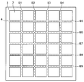
- FIG. 2 shows a first example of the magnetic ribbon 2 arranged on one resin film portion 3. 2 to 9, 2 is a magnetic ribbon, 3 is a resin film, and 4 is a cut portion. S is the width of the cut portion 4.
- the shape of the cut portion 4 may be either a shape that separates the magnetic ribbons 2 shown in FIG. 2 or a slit shape that cuts a part of the magnetic ribbon 2 shown in FIG. 4.
- FIG. 2 shows a state in which a gap is provided between the magnetic ribbons 2 for easy understanding, but the adjacent magnetic ribbons 2 may be in contact with each other (the width S of the cut portion 4 is 0 mm).
- the cut portion 4 is preferably 10% or less of the whole, and more preferably all the widths S are 1 mm or less (including 0).
- the width S of the cut portion 4 is preferably 0.5 mm or less.
- the cut portion 4 preferably has a shape penetrating from the front surface to the back surface of the magnetic ribbon 2, whereby a high Q value can be obtained. For example, sufficient characteristics cannot be obtained with a notch that does not penetrate, such as a recess or groove.
- the cut portion 4 in this embodiment does not include a cut that does not penetrate, such as a recess or a groove.
- the ratio of the total length B of the cut portions 4 provided in the magnetic ribbon 2 to the total outer peripheral length A of the outer peripheral region of the magnetic ribbon 2 arranged on one resin film 3. (B / A) is in the range of 2 to 25.
- the total outer peripheral length A of the outer peripheral region of the magnetic ribbon 2 is the outermost peripheral length of the magnetic ribbon 2 (which may be divided or not divided) disposed on one surface of the magnetic sheet 1. It is.
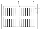
- the total outer peripheral length A of the outer peripheral region of the magnetic ribbon 2 is obtained from “A1 + A2 + A3 + A4” as shown in FIG. FIG.
- the outer peripheral length is also referred to as the outer peripheral length A in the case of other shapes. Since the cut portion 4 serving as a gap between the magnetic ribbons 2 has a width as small as 1 mm or less, the total outer circumferential length A of the outer circumferential region of the magnetic ribbon 2 is obtained by the above-described method.
- FIG. 3 shows how to obtain the total length B of the cut portions 4 provided in the magnetic ribbon 2.
- the total length B of the cut portions 4 is obtained from “B1 + B2 + B3 + B4 + B5 + B6 + B7 + B8 + B9”. If the width of B1 to B8 is 0.5 mm and the width of B9 is 2 mm, the total length B of the cut portions 4 is “B1 + B2 + B3 + B4 + B5 + B6 + B7 + B8”. As shown in FIG.
- the width S is 1 mm among the gap and the slit.
- the total length of the following cut portions 4 (including 0) is defined as B.
- the slit penetrates from the front surface to the back surface.
- the magnetic ribbon 2 having the slit-like cut portions 4 is easy to handle.
- the notch 4 formed by arranging the magnetic ribbons 2 with a gap is easy to adjust the width S in the range of 0 to 1 mm.
- the size of one piece is preferably 0.5 mm ⁇ 0.5 mm or more.
- the handleability is poor, and it is difficult to arrange the cut portions 4 so that the width S is in the range of 0 to 1 mm.
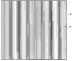
- one magnetic ribbon 2 may be disposed on the entire surface of the resin film portion 3, and a number of slits may be provided in the magnetic ribbon 2.
- the shape of the cut portion 4 is not limited to a linear shape, and may be a curved shape or a zigzag shape.
- FIG. 5 shows an example in which a plurality of slits (cuts 4) are provided in one magnetic ribbon 2.
- FIG. 5 shows an example in which the slit (cut portion 4) is not formed up to the end of the magnetic ribbon 2. In this case, since all the cut portions 4 can be provided in one magnetic ribbon 2, it is only necessary to place the magnetic ribbon 2 on the resin film portion 3. Therefore, it is easy to form a laminate of the magnetic ribbon 2 and the resin film portion 3.
- FIG. 6 shows an example in which a plurality of slits (notches 4) are provided from one end of the magnetic ribbon 2 to the opposite end.
- a large number of cut portions 4 having a constant width S are formed at a time by pasting the magnetic ribbon 2 before forming the cut portions 4 on the resin film portion 3 and then slitting the magnetic ribbon 2. It is possible to form the cut portion 4 easily.
- FIG. 7 shows an example in which a large number of cross-shaped cut portions 4 are provided in the magnetic ribbon 2.
- the shape of the cut portion 4 is not limited to a linear shape as shown in FIGS. 5 and 6, and may be a cross shape as shown in FIG.
- the cross-shaped cut portion 4 can be formed by an etching method.
- FIGS. 5 to 7 are examples in which a plurality of cut portions 4 are provided in one magnetic ribbon 2.
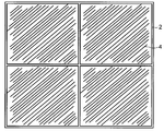
- FIG. 4 shows an example in which a plurality of magnetic ribbons 2 provided with the cut portions 4 are arranged on the resin film portion 3, the shape shown in FIGS. 8 and 9 may be used in addition to this.
- FIG. 8 shows an example in which four triangular magnetic ribbons 2 provided with a plurality of slits (cuts 4) are arranged in a square shape.
- the width S of the cut portion 4 can be controlled by both the slit width and the gap between the adjacent magnetic ribbons 2.
- FIG. 9 shows an example in which the magnetic ribbon 2 is provided with an oblique slit (cut portion 4). The slit may be formed obliquely.
- the method for forming the cut portion 4 is not particularly limited. For example, a method of cutting a long magnetic thin ribbon into a desired size with a cutting blade, a method of forming a slit by etching, and forming a slit by laser processing And the like.
- the cut portion 4 may be formed by combining these methods.
- the cut portion 4 may be formed after the magnetic ribbon 2 is arranged on the resin film portion 3, or the magnetic ribbon 2 in which the cut portion 4 is formed in advance may be arranged in the resin film portion 3.
- the cut portions 4 may be formed uniformly on the entire magnetic ribbon 2, or may be formed in a sparse / dense state so that the vicinity of the center of the magnetic ribbon 2 is dense, for example.
- the shape of the cut portion 4 formed in each magnetic ribbon 2 in the laminated structure may be different.
- the B / A ratio of the magnetic sheet 1 of this embodiment is controlled in the range of 2 to 25, the L value and Q value of the magnetic sheet 1 can be improved.
- a magnetic sheet having an L value of 11 ⁇ H or more and a Q value of 10 or more at 125 kHz can be obtained.
- the Q value does not improve, and when the B / A ratio exceeds 25, the L value decreases.
- the B / A ratio is less than 2
- the generation of eddy currents cannot be suppressed, and if the B / A ratio exceeds 25, the power receiving efficiency decreases.
- the decrease in power reception efficiency becomes a factor that increases the charging time.
- the B / A ratio on each resin film portion 3 is preferably in the range of 2 to 25.
- the B / A ratios on the respective resin film portions 3 may all be the same, or the B / A ratio may be changed for each resin film portion.
- a resonance circuit is applied to a power receiving device (electronic device to be charged) in order to increase power receiving efficiency.
- a resonant circuit configured by connecting L (inductor) and C (capacitor) in series or in parallel maximizes or minimizes the current flowing in the circuit at a specific resonant frequency.
- the frequency f is increased, L is increased, and the loss R is decreased.
- the frequency f can be increased by circuit design, but if the frequency f increases, the eddy current loss increases and the loss R increases.
- an increase in eddy current loss is prevented by using the magnetic sheet 1 having the magnetic ribbon 2 formed with the cut portions 4 of a predetermined amount (B / A is 2 to 25).
- An eddy current is an annular current that is excited in a conductor by electromagnetic induction when the magnitude of a magnetic field applied to the conductor changes, and a loss that occurs with this is an eddy current loss.
- Heat generation occurs when the eddy current increases due to electromagnetic induction. For example, in a power receiving device equipped with a secondary battery, the case of the secondary battery generates heat due to eddy current, and the charge / discharge cycle life is shortened or the deterioration of the discharge capacity is promoted. Excessive heat generation may cause electronic device failure.
- FIGS. 10 and 11 show the configuration of the electronic apparatus according to the first and second embodiments.
- An electronic device 10 shown in FIGS. 10 and 11 includes a power receiving device 11 and an electronic device main body 12 to which a non-contact charging method is applied.
- the main body of the electronic device 12 includes a circuit board 13 and an electronic device 14 mounted thereon.
- the power receiving device 11 and the electronic device main body 12 are arranged in a housing 15, and the electronic device 10 is configured by these.
- the power receiving device 11 includes a power receiving coil 16 having a spiral coil, a rectifier 17 that rectifies an AC voltage generated in the power receiving coil 16, and a secondary battery 18 that is charged with the DC voltage rectified by the rectifier 17. .
- the electronic device main body 12 includes an electronic device 14 that operates by being supplied with a DC voltage charged to the secondary battery 18 of the power receiving device 11.
- the electronic device main body 12 may include components, devices, and the like corresponding to the functions and operations of the electronic device 10.
- a planar coil in which a metal wire such as a copper wire is wound in a planar state, a planar coil formed by printing a metal powder paste in a spiral shape, or the like is used.
- the winding shape of the spiral coil is not particularly limited, such as a circle, an ellipse, a rectangle, and a polygon.
- the number of turns of the spiral coil is also appropriately set according to the required characteristics.
- the rectifier 17 examples include semiconductor elements such as transistors and diodes.
- the number of rectifiers 17 is arbitrary, and one or more rectifiers 17 are used as necessary.
- the rectifier 17 may be formed by a film forming technique such as TFT. 10 and 11, the rectifier 17 is installed on the power receiving coil 16 side of the circuit board 13.
- the rectifier 17 may be provided on the surface of the circuit board 13 opposite to the power receiving coil 16.
- the secondary battery 18 can be charged / discharged, and various shapes such as a flat plate type and a button type can be used.
- the electronic device 14 includes various elements and parts constituting a circuit, such as a resistance element, a capacitance element, an inductance element, a control element, and a memory element. Furthermore, components and devices other than these may be used.
- the circuit board 13 is obtained by forming a circuit on the surface or inside of an insulating substrate such as a resin substrate or a ceramic substrate.
- the electronic device 14 is mounted on the circuit board 13.
- the electronic device 14 may include those not mounted on the circuit board 13.
- the electronic device 10 of the first embodiment includes a magnetic sheet 1 installed between a spiral coil (power receiving coil) 16 and a secondary battery 18 as shown in FIG. That is, the spiral coil 16 and the secondary battery 18 are disposed with the magnetic sheet 1 interposed therebetween.
- the spiral coil 16 has a flat portion as at least a part thereof, and the flat portion is disposed along the surface of the magnetic sheet 1.
- the magnetic sheet 1 is disposed between the spiral coil 16 and the secondary battery 18 constituting the power receiving device 11.
- the electronic device 10 of the second embodiment includes the magnetic sheet 1 installed between the secondary battery 18 and the circuit board 13. Further, the magnetic sheet 1 may be disposed between the spiral coil 16 and the rectifier 17 or between the spiral coil 16 and the electronic device 14. The magnetic sheet 1 is disposed at one or more of these locations. The magnetic sheet 1 may be disposed at two or more locations.
- the configuration of the electronic device 10 is not limited to FIGS.
- the arrangement of the spiral coil 16, the secondary battery 18, and the circuit board 13 can be variously changed.
- a secondary battery, a circuit board, and a spiral coil may be sequentially arranged from the upper side.
- the magnetic sheet 1 is disposed between, for example, a circuit board and a spiral coil.
- the spiral coil 16 / magnetic sheet 1 / circuit board 13 may be simply laminated, or the space between them may be fixed with an adhesive or a brazing material. May be. The same applies to other cases, and each component may be simply laminated, or may be fixed with an adhesive or a brazing material.
- the magnetic sheet 1 can shield the magnetic flux passing through the spiral coil 16 during charging. Accordingly, since the magnetic flux interlinking with the circuit board 13 and the like inside the electronic device 10 is reduced, the generation of eddy current due to electromagnetic induction can be suppressed.
- the thickness of the magnetic sheet 1 is preferably in the range of 1 mm or less in consideration of installation properties, magnetic flux blocking properties, and the like.
- the magnetic sheet 1 of the above-described embodiment is used as, for example, an inductor magnetic body or a magnetic shield magnetic body (including a noise countermeasure sheet).
- it is suitable for a magnetic sheet used in a frequency band of 100 kHz or higher. That is, the effect of improving the Q value and the effect of reducing the eddy current loss based on the magnetic ribbon 2 having the cut portion 4 are better exhibited in a frequency band of 100 kHz or more. Therefore, the magnetic sheet 1 is suitable as a magnetic body for an inductor or a magnetic body for a magnetic shield used in a frequency band of 100 kHz or higher.
- the electronic device 10 of this embodiment is suitable for a mobile phone, a portable audio device, a digital camera, a game machine, and the like. Such an electronic device 10 is set in a power feeding device and non-contact charging is performed.
- FIG. 12 shows a configuration of the non-contact charging apparatus according to the embodiment.
- the non-contact charging device 20 includes an electronic device 10 and a power feeding device 30.
- the electronic device 10 is the one shown in the above-described embodiment.
- the power feeding device 30 includes a magnet 32 that aligns the power feeding coil 31 and the power receiving device 11 and a power source that applies an AC voltage to the power feeding coil 31 (not shown).
- the power feeding coil 31 is arranged in a non-contact manner with the power receiving coil 11.
- Charging by the non-contact charging device 20 is performed as follows. An AC voltage is applied from the power source to the power supply coil 31 of the power supply device 30 to generate a magnetic flux in the power supply coil 31. The magnetic flux generated in the power feeding coil 31 is transmitted to the power receiving coil 16 arranged in non-contact with the power feeding coil 31. The receiving coil 16 receives magnetic flux and generates an AC voltage by electromagnetic induction. This AC voltage is rectified by the rectifier 17. The DC voltage rectified by the rectifier 17 is charged in the secondary battery 18.
- the power feeding device 30 may be mounted with components (not shown) such as a magnetic core for controlling magnetic flux.
- Non-contact charging device A charging system for mobile phones was prepared as a non-contact charging device.
- the power feeding device converts power from an AC power source into a constant electromagnetic wave through a control circuit, and arranges a primary coil (feeding coil) for transmitting the electromagnetic wave in the vicinity of a table.
- An NdFeB bond magnet residual magnetic flux density (Br): 0.75 T, coercive force (Hc): 760 kA / m) having a diameter of 15 mm and a thickness of 0.5 mm was disposed at the center of the primary coil.
- the cellular phone includes a secondary coil (power receiving coil) formed of a spiral coil as a power receiving device, a circuit board on which a rectifier that rectifies AC power generated in the secondary coil is mounted, and a secondary battery.
- the secondary coil is a copper wire wound in a flat shape around an outer circumference of 30 mm and an inner circumference of 23 mm.
- Comparative Example A In the above mobile phone, the power receiving device is configured without using a magnetic sheet. A mobile phone and a non-contact charging device using this were used as Comparative Example A.
- Examples 1 to 7, Comparative Examples 1 to 3 A long amorphous alloy ribbon (magnetic ribbon) having a composition of Fe 66 Co 18 Si 1 B 15 , a thickness of 20 ⁇ m and a width of 50 mm was produced by a single roll method. This magnetic ribbon had a saturation magnetization of 1.8 T and a saturation magnetostriction constant of 32 ppm. Since the obtained magnetic ribbon was used without being heat-treated, it could be bent at 180 °.
- Ratio of A (total outer peripheral length of the outer peripheral area of the magnetic ribbon disposed on the same resin film portion) and B (total length of the cut portion having a width of 1 mm or less (including 0) provided on the magnetic ribbon) (B / A) is the range shown in Table 1. Twelve of these were laminated to produce a magnetic sheet according to the example. The magnetic sheet was shaped to completely cover the magnetic ribbon with the resin film part. The thickness of each magnetic sheet is in the range of 0.54 to 0.56 mm.
- the same magnetic ribbon with no slit (notch) formed is Comparative Example 1, the B / A ratio is 1 as Comparative Example 2, and the B / A ratio is 28 is Comparative Example 3.
- stacked 12 sheets of these similarly to the Example was produced.
- the magnetic sheet was shaped to completely cover the magnetic ribbon with the resin film part.
- Example 8 to 12 Comparative Examples 4 to 9
- a long amorphous alloy ribbon having a composition of Fe 66 Co 18 Si 1 B 15 , a thickness of 22 ⁇ m and a width of 50 mm was produced by a single roll method.
- This magnetic ribbon had a saturation magnetization of 1.8 T and a saturation magnetostriction constant of 32 ppm. Since the obtained magnetic ribbon was used without being heat-treated, it could be bent at 180 °.
- an amorphous alloy ribbon (plate thickness: 17 ⁇ m) having a Co 68 Fe 4.5 Cr 2.5 Si 15 B 10 composition with a saturation magnetostriction constant of zero was prepared. A cut portion (the width was unified at 0.5 mm) with a B / A ratio of 1 was formed on this.
- the magnetic ribbons were laminated in the number shown in Table 2 to produce magnetic sheets of Comparative Examples 4-9. Table 2 shows the thickness of the magnetic sheet.
- Example 13 to 38 Comparative Examples 10 to 28
- An amorphous alloy ribbon having the composition shown in Table 3 and a width of 50 mm was produced by a single roll method.
- the saturation magnetization, saturation magnetostriction constant, and plate thickness of each ribbon are as shown in Table 3. Since the obtained magnetic ribbon was used without being heat-treated, it could be bent at 180 °.
- the magnetic ribbon was cut into 20 mm ⁇ 20 mm, and various numbers of slits (cuts) having a length of 10 to 15 mm penetrating in the thickness direction of the magnetic ribbon were formed by etching. .
- the width of the slit (cut portion) formed by etching was unified to 0.1 mm.
- 4 sheets were affixed as shown in FIG. 4 on the PET film (thickness 80 micrometers) which apply
- the B / A ratio is as shown in Table 3.
- the PET film was peeled off from this sample, and 10 magnetic ribbons were laminated via an adhesive layer to produce magnetic sheets of Examples 13 to 38. Table 3 shows the thickness of the magnetic sheet.
- Example 39 An amorphous alloy ribbon (magnetic ribbon) having a composition of Fe 66 Co 18 Si 1 B 15 , a plate thickness of 16 ⁇ m, and a width of 50 mm was produced by a single roll method. Table 3 shows the saturation magnetization and saturation magnetostriction constant of the magnetic ribbon. Since the obtained magnetic ribbon was used without being heat-treated, it could be bent at 180 °. Next, the magnetic ribbon was cut into a length of 41 mm and a width of 1 mm. Forty-one magnetic ribbons after cutting were arranged on a PET film (thickness 25 ⁇ m) coated with an acrylic adhesive (thickness 10 ⁇ m) so that the gap was 0 mm (contact arrangement). Ten magnetic sheets were laminated to produce a magnetic sheet of Example 39. The surface of the magnetic ribbon was covered with a resin film part. The thickness of the magnetic sheet is 0.34 mm.
- the Q value and L value were measured using an impedance analyzer (HP4192A).
- the coupling efficiency power receiving efficiency
- the heat generation amount were measured. The coupling efficiency was evaluated by how much power can be transmitted to the secondary coil (power receiving coil) when a constant power (1 W) is transmitted from the primary coil (power feeding coil).
- the amount of generated heat was measured by measuring the temperature rise after 2 hours of power transmission at a transmission rate of 0.4 W / h and 1.5 W / h for 2 hours.
- ⁇ when the temperature rise exceeds 25 ° C. and is 40 ° C. or less, ⁇ , and when the temperature rise exceeds 40 ° C.
- it unified at room temperature 25 degreeC before power transmission.
- the fact that the temperature rise is small means that the generation of eddy current is prevented.
- the non-contact charging device using the magnetic sheet of the example has high coupling efficiency and low heat generation. It has been confirmed that a magnet is disposed in the power feeding device and exhibits excellent characteristics even in an environment where magnetic saturation is likely to occur.
- the non-contact charging device using the magnetic sheet of the comparative example had a low coupling efficiency and a large amount of heat generation.
- the magnetic sheet of the comparative example is magnetically saturated because the magnet is arranged in the power feeding device.
- the magnetic sheet of the embodiment is particularly effective for a non-contact charging device in which a magnet is disposed in a power feeding device (positioning of a power receiving device by a magnet).
- a thinner magnetic sheet can be provided by making the PET films on the upper and lower surfaces of the magnetic sheet into a thin material or by thinning the adhesive layer.
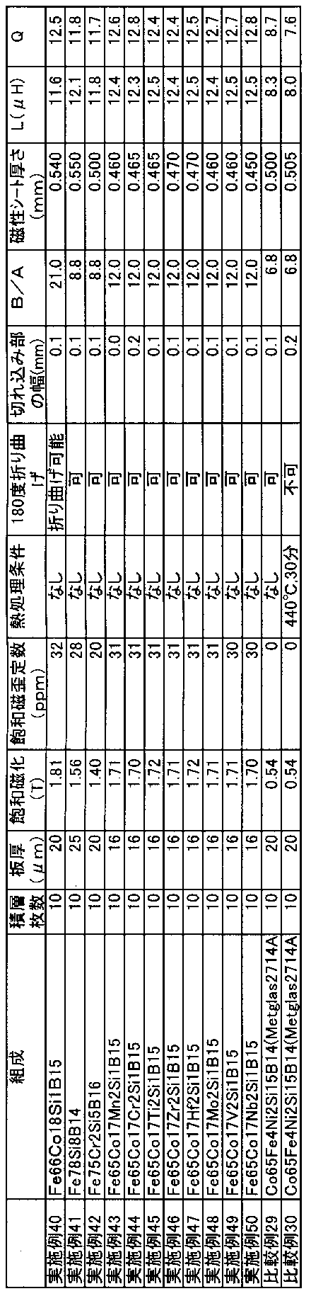
- Examples 40 to 50, Comparative Examples 29 to 30 Magnetic sheets of Examples 40 to 50 and Comparative Examples 29 to 30 shown in Table 5 were prepared. Next, the Q value and L value of the magnetic sheet were measured using an impedance analyzer (HP4192A). The results are also shown in Table 5.
- the power feeding device converts power from an AC power source (0.5 A or 1.0 A) into a constant electromagnetic wave through a control circuit, and a primary coil (feeding coil) for transmitting the electromagnetic wave is arranged near the pedestal.
- a primary coil feeding coil
- any one of an NdFeB sintered magnet, a ferrite sintered magnet, and an SmCo sintered magnet having a diameter of 15 mm and a thickness of 0.5 mm was disposed at the center of the primary coil.
- the cellular phone includes a secondary coil (power receiving coil) formed of a spiral coil as a power receiving device, a circuit board on which a rectifier that rectifies AC power generated in the secondary coil is mounted, and a secondary battery.
- the secondary coil is a copper wire wound in a flat shape around an outer circumference of 30 mm and an inner circumference of 23 mm.
- the coupling efficiency and calorific value when the AC power source current was changed to 0.5 A or 1.0 A and the magnet was changed to a NdFeB sintered magnet, a ferrite sintered magnet, or a SmCo sintered magnet were measured.
- the magnet characteristics are as shown in Table 6.
- the coupling efficiency is such that when the constant current (1 W) is transmitted from the primary coil (feeding coil) using the above-described non-contact charging device and the current value of the AC power source is set to 0.5 A or 1.0 A. Evaluation was made based on whether electric power could be transmitted to the secondary coil (receiving coil).
- the coupling efficiency (the amount of electric power transmitted to the secondary coil) of Comparative Example A is 100, the ones improved by 20% or more and less than 40% (120 or more and less than 140) are ⁇ , 40 % (140 or more) improved, and less than 20% (less than 120) are indicated by x.
- High coupling efficiency means good power reception efficiency.
- the amount of heat generated was measured by measuring the temperature increase after 2 hours of power transmission for 2 hours when the current value of the AC power supply was 0.5 A or 1.0 A.
- the temperature rise is 25 ° C. or less, ⁇ , when the temperature rise exceeds 25 ° C. and is 40 ° C. or less, ⁇ , and when the temperature rise exceeds 40 ° C.
- it unified at room temperature 25 degreeC before power transmission.
- the fact that the temperature rise is small means that the generation of eddy current is prevented. Table 7 shows the measurement results.
- the magnetic sheets of the examples exhibited excellent characteristics even when the current value of the AC power source was changed. Moreover, even when the type of magnet was changed, excellent characteristics were exhibited. Thus, even when the material of the AC power source or the positioning magnet is changed, according to the magnetic sheet of the embodiment, it is possible to improve the power receiving efficiency and reduce the heat generation amount. For this reason, the reliability of a power receiving device or a non-contact charging device can be greatly improved.
Landscapes
- Engineering & Computer Science (AREA)
- Power Engineering (AREA)
- Computer Networks & Wireless Communication (AREA)
- Physics & Mathematics (AREA)
- Electromagnetism (AREA)
- Chemical & Material Sciences (AREA)
- Dispersion Chemistry (AREA)
- Charge And Discharge Circuits For Batteries Or The Like (AREA)
- Regulation Of General Use Transformers (AREA)
- Coils Or Transformers For Communication (AREA)
- Soft Magnetic Materials (AREA)
Abstract
Description
一般式:Fe100-a-b-cMaXbTc …(1)
(式中、MはNiおよびCoから選ばれる少なくとも1種の元素、TはMn、Cr、Ti、Zr、Hf、Mo、V、Nb、W、Ta、Cu、Snおよび希土類元素から選ばれる少なくとも1種の元素、XはB、Si、CおよびPから選ばれる少なくとも1種の元素であり、a、bおよびcは0≦a≦25原子%、10≦b≦35原子%、0≦c≦5原子%を満足する数である)
で表される組成を有するアモルファス合金薄帯を1枚以上備えることが好ましい。
非接触充電装置として携帯電話機用の充電システムを用意した。給電装置はAC電源からの電力を制御回路を通して一定の電磁波に変換し、この電磁波を送信する一次コイル(給電コイル)を置き台の近傍に配置したものである。なお、一次コイルの中心部には直径15mm、厚さ0.5mmのNdFeB系ボンド磁石(残留磁束密度(Br):0.75T、保磁力(Hc):760kA/m)を配置した。携帯電話機は受電装置としてスパイラルコイルからなる二次コイル(受電コイル)と二次コイルに生じた交流電力を整流する整流器が実装された回路基板と二次電池とを具備している。二次コイルは銅線を外周30mm、内周23mmに平面状に巻回したものである。
上記した携帯電話機において、磁性シートを用いずに受電装置を構成した。これを用いた携帯電話機と非接触充電装置を比較例Aとした。
Fe66Co18Si1B15組成を有し、厚さが20μm、幅が50mmの長尺なアモルファス合金薄帯(磁性薄帯)を単ロール法で作製した。この磁性薄帯の飽和磁化は1.8Tであり、飽和磁歪定数は32ppmであった。得られた磁性薄帯は熱処理せずに用いるため、180°に折り曲げ可能であった。
Fe66Co18Si1B15組成を有し、厚さが22μm、幅が50mmの長尺なアモルファス合金薄帯(磁性薄帯)を単ロール法で作製した。この磁性薄帯の飽和磁化は1.8Tであり、飽和磁歪定数は32ppmであった。得られた磁性薄帯は熱処理せずに用いるため、180°に折り曲げ可能であった。
表3に示す組成を有し、幅が50mmのアモルファス合金薄帯を単ロール法で作製した。各薄帯の飽和磁化、飽和磁歪定数、板厚は表3に示す通りである。得られた磁性薄帯は熱処理せずに用いるため、180°に折り曲げ可能であった。
Fe66Co18Si1B15組成を有し、板厚が16μm、幅が50mmのアモルファス合金薄帯(磁性薄帯)を単ロール法で作製した。磁性薄帯の飽和磁化、飽和磁歪定数は表3に示す通りである。得られた磁性薄帯は熱処理せずに用いるため、180°に折り曲げ可能であった。次に、磁性薄帯を縦41mm×横1mmに切断した。切断後の磁性薄帯41本を、隙間が0mm(接触配置)となるように、アクリル系接着剤(厚さ10μm)を塗布したPETフィルム(厚さ25μm)上に並べた。これを10枚積層して実施例39の磁性シートを作製した。磁性薄帯の表面は全て樹脂フィルム部で覆った構造とした。磁性シートの厚さは0.34mmである。


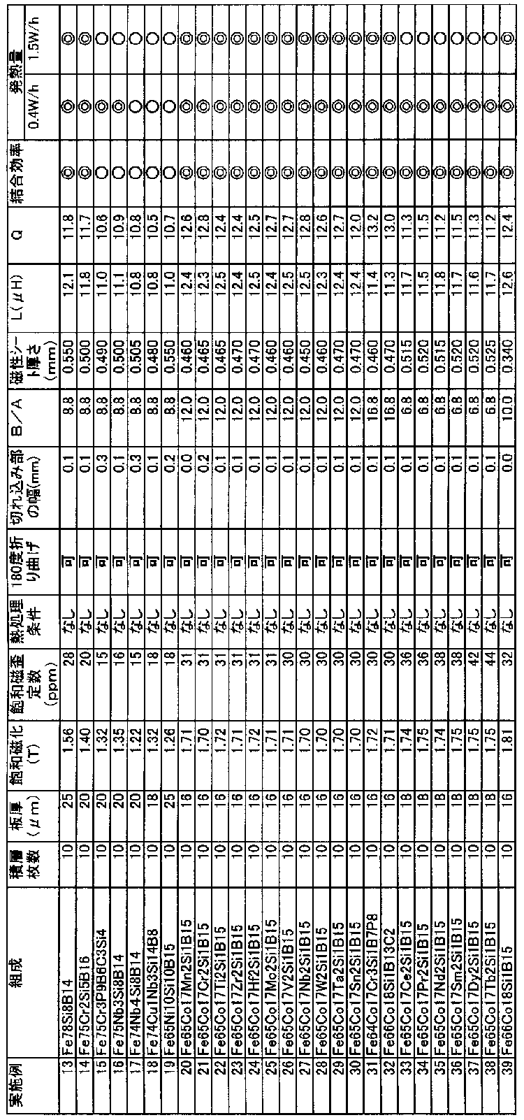

表5に示す実施例40~50および比較例29~30の磁性シートを用意した。次に、インピーダンスアナライザ(HP4192A)を用いて、磁性シートのQ値とL値を測定した。その結果を表5に合わせて示す。


Claims (15)
- 複数の磁性薄帯と樹脂フィルム部との積層体を具備する磁性シートであって、
前記積層体は5~25枚の範囲で積層された前記磁性薄帯を備え、前記磁性薄帯には1mm以下(0を含む)の幅を有する切り込み部が設けられており、
1つの前記樹脂フィルム部上に配置された前記磁性薄帯の外周領域の合計外周長をA、前記磁性薄帯に設けられた前記切り込み部の合計長さをBとしたとき、前記磁性薄帯の合計外周長Aに対する前記切り込み部の合計長さBの比(B/A)が2以上25以下の範囲であることを特徴とする磁性シート。 - 請求項1記載の磁性シートにおいて、
前記磁性薄帯と前記樹脂フィルム部とは交互に積層されていることを特徴とする磁性シート。 - 請求項1記載の磁性シートにおいて、
前記積層体は前記切り込み部の幅が全て1mm以下(0含む)である前記磁性薄帯を1枚以上備えることを特徴とする磁性シート。 - 請求項1記載の磁性シートにおいて、
前記積層体は、前記磁性薄帯として、
一般式:Fe100-a-b-cMaXbTc
(式中、MはNiおよびCoから選ばれる少なくとも1種の元素、TはMn、Cr、Ti、Zr、Hf、Mo、V、Nb、W、Ta、Cu、Snおよび希土類元素から選ばれる少なくとも1種の元素、XはB、Si、CおよびPから選ばれる少なくとも1種の元素であり、a、bおよびcは0≦a≦25原子%、10≦b≦35原子%、0≦c≦5原子%を満足する数である)
で表される組成を有するアモルファス合金薄帯を1枚以上備えることを特徴とする磁性シート。 - 請求項1記載の磁性シートにおいて、
前記切り込み部は前記磁性薄帯を切り離す形状を有することを特徴とする磁性シート。 - 請求項1記載の磁性シートにおいて、
前記切り込み部は前記磁性薄帯の一部を切断する形状を有することを特徴とする磁性シート。 - 請求項1記載の磁性シートにおいて、
前記積層体は5~30μmの範囲の板厚を有する前記磁性薄帯を1枚以上備えることを特徴とする磁性シート。 - 請求項1記載の磁性シートにおいて、
前記積層体は180度密着折り曲げを行った際に破壊しない前記磁性薄帯を1枚以上備えることを特徴とする磁性シート。 - 請求項1記載の磁性シートにおいて、
前記積層体は15ppm以上の飽和磁歪定数を有する前記磁性薄帯を1枚以上備えることを特徴とする磁性シート。 - 請求項1記載の磁性シートにおいて、
前記積層体は1.2T以上2.1T以下の範囲の飽和磁束密度を有する前記磁性薄帯を1枚以上備えることを特徴とする磁性シート。 - スパイラルコイルを有する受電コイルと、
前記受電コイルに発生した交流電圧を整流する整流器と、
前記整流器で整流された直流電圧が充電される二次電池と、
前記スパイラルコイルと前記二次電池との間、および前記スパイラルコイルと前記整流器との間の少なくとも1箇所に配置された、請求項1記載の磁性シートと
を具備することを特徴とする非接触受電装置。 - スパイラルコイルを有する受電コイルと、前記受電コイルに発生した交流電圧を整流する整流器と、前記整流器で整流された直流電圧が充電される二次電池とを備える非接触受電装置と、
前記二次電池から前記直流電圧が供給されて動作する電子デバイスと、前記電子デバイスが実装された回路基板とを備える電子機器本体と、
前記スパイラルコイルと前記二次電池との間、前記スパイラルコイルと前記整流器との間、前記スパイラルコイルと前記電子デバイスとの間、および前記スパイラルコイルと前記回路基板との間の少なくとも1箇所に配置された、請求項1記載の磁性シートと
を具備することを特徴とする電子機器。 - 請求項12記載の電子機器と、
前記電子機器の前記受電コイルと非接触で配置される給電コイルと、前記給電コイルに交流電圧を印加する電源と、位置合せ用の磁石とを備える給電装置とを具備し、
前記磁石で前記電子機器を位置合せした上で、前記給電コイルに発生させた磁束を前記受電コイルに伝達して電力を非接触で伝送することを特徴とする非接触充電装置。 - 請求項13記載の非接触充電装置において、
前記磁石はNd-Fe-B基磁石であることを特徴とする非接触充電装置。 - 請求項13記載の非接触充電装置において、
前記磁性シートは磁気シールドまたはインダクタとして配置されることを特徴とする非接触充電装置。
Priority Applications (5)
| Application Number | Priority Date | Filing Date | Title |
|---|---|---|---|
| CN201280020139.1A CN103493158B (zh) | 2011-04-25 | 2012-04-24 | 磁性片和使用其的非接触受电装置、电子设备及非接触充电装置 |
| KR1020137030734A KR101559223B1 (ko) | 2011-04-25 | 2012-04-24 | 자성 시트와 그것을 사용한 비접촉 수전 장치, 전자 기기 및 비접촉 충전 장치 |
| JP2013511929A JP5917496B2 (ja) | 2011-04-25 | 2012-04-24 | 磁性シートとそれを用いた非接触受電装置、電子機器および非接触充電装置 |
| US14/062,472 US10083785B2 (en) | 2011-04-25 | 2013-10-24 | Magnetic sheet and non-contact power receiving device, electronic apparatus and non-contact charging system using the same |
| US16/139,803 US11417449B2 (en) | 2011-04-25 | 2018-09-24 | Magnetic sheet and non-contact power receiving device, electronic apparatus and non-contact charging system using the same |
Applications Claiming Priority (2)
| Application Number | Priority Date | Filing Date | Title |
|---|---|---|---|
| JP2011097470 | 2011-04-25 | ||
| JP2011-097470 | 2011-04-25 |
Related Child Applications (1)
| Application Number | Title | Priority Date | Filing Date |
|---|---|---|---|
| US14/062,472 Continuation US10083785B2 (en) | 2011-04-25 | 2013-10-24 | Magnetic sheet and non-contact power receiving device, electronic apparatus and non-contact charging system using the same |
Publications (1)
| Publication Number | Publication Date |
|---|---|
| WO2012147341A1 true WO2012147341A1 (ja) | 2012-11-01 |
Family
ID=47071871
Family Applications (1)
| Application Number | Title | Priority Date | Filing Date |
|---|---|---|---|
| PCT/JP2012/002818 Ceased WO2012147341A1 (ja) | 2011-04-25 | 2012-04-24 | 磁性シートとそれを用いた非接触受電装置、電子機器および非接触充電装置 |
Country Status (5)
| Country | Link |
|---|---|
| US (2) | US10083785B2 (ja) |
| JP (1) | JP5917496B2 (ja) |
| KR (1) | KR101559223B1 (ja) |
| CN (1) | CN103493158B (ja) |
| WO (1) | WO2012147341A1 (ja) |
Cited By (22)
| Publication number | Priority date | Publication date | Assignee | Title |
|---|---|---|---|---|
| CN103841812A (zh) * | 2012-11-26 | 2014-06-04 | 胜美达集团株式会社 | 磁性薄板、电子仪器及磁性薄板的制造方法 |
| WO2014096040A1 (de) * | 2012-12-21 | 2014-06-26 | Robert Bosch Gmbh | Induktivladespulenvorrichtung |
| WO2014103275A1 (ja) * | 2012-12-27 | 2014-07-03 | 株式会社 東芝 | 非接触受電装置用磁性シートとそれを用いた非接触受電装置、電子機器、および非接触充電装置 |
| KR20140102033A (ko) * | 2013-02-13 | 2014-08-21 | 엘지이노텍 주식회사 | 자성시트 및 이를 포함하는 무선 전력 수신 장치 |
| KR20140105333A (ko) * | 2013-02-22 | 2014-09-01 | 삼성전자주식회사 | 무선 전력 전송 장치 |
| WO2014162177A1 (de) * | 2013-04-02 | 2014-10-09 | Vacuumschmelze Gmbh & Co. Kg | Gegenstand mit kabelloser ladevorrichtung und verfahren zum herstellen einer abschirmfolie |
| WO2014166969A1 (en) * | 2013-04-09 | 2014-10-16 | Bombardier Transportation Gmbh | Receiving device with coil of electric line for receiving a magnetic field and for producing electric energy by magnetic induction and with magnetizable material |
| CN104283326A (zh) * | 2013-07-10 | 2015-01-14 | 星电株式会社 | 无接点供电机构以及无接点供电装置用电磁感应线圈 |
| JP2015019495A (ja) * | 2013-07-10 | 2015-01-29 | ホシデン株式会社 | 無接点給電機構 |
| JP2015192521A (ja) * | 2014-03-28 | 2015-11-02 | デクセリアルズ株式会社 | 非接触給電用アンテナシステム、及び電子機器 |
| JP2016101344A (ja) * | 2014-11-28 | 2016-06-02 | コニカミノルタ株式会社 | 生体情報測定装置 |
| JP2016139694A (ja) * | 2015-01-27 | 2016-08-04 | 東洋インキScホールディングス株式会社 | 非接触電力伝送用磁性シート |
| US9806540B2 (en) | 2013-04-09 | 2017-10-31 | Bombardier Transportation Gmbh | Receiving device for receiving a magnetic field and for producing electric energy by magnetic induction |
| EP2775484A3 (en) * | 2013-03-06 | 2017-11-22 | Kabushiki Kaisha Toshiba | Coil, power receiving apparatus and power transmitting apparatus |
| JP2018056578A (ja) * | 2017-11-17 | 2018-04-05 | 東洋インキScホールディングス株式会社 | 非接触電力伝送用磁性シート |
| JP2018537931A (ja) * | 2015-09-04 | 2018-12-20 | アモセンス・カンパニー・リミテッドAmosense Co., Ltd. | 磁気共振方式無線電力転送用磁場遮蔽ユニット、これを含む無線電力転送モジュール及び電子装置 |
| CN110168854A (zh) * | 2016-12-20 | 2019-08-23 | 韦特里西提公司 | 具有改善效率的用于感应式功率传输的磁结构 |
| WO2022181183A1 (ja) * | 2021-02-26 | 2022-09-01 | 株式会社村田製作所 | インダクタ部品 |
| WO2024024958A1 (ja) * | 2022-07-29 | 2024-02-01 | 株式会社プロテリアル | シート状磁性部材 |
| WO2024043283A1 (ja) * | 2022-08-23 | 2024-02-29 | 株式会社プロテリアル | シート状磁性部材 |
| WO2024241687A1 (ja) * | 2023-05-23 | 2024-11-28 | 株式会社プロテリアル | シート状磁性部材 |
| WO2025243746A1 (ja) * | 2024-05-22 | 2025-11-27 | ソニーセミコンダクタソリューションズ株式会社 | 半導体装置 |
Families Citing this family (25)
| Publication number | Priority date | Publication date | Assignee | Title |
|---|---|---|---|---|
| US9230732B2 (en) * | 2012-01-17 | 2016-01-05 | Texas Instruments Incorporated | Wireless power transfer |
| TW201421211A (zh) * | 2012-11-16 | 2014-06-01 | 致伸科技股份有限公司 | 無線充電裝置 |
| US9142990B2 (en) * | 2013-01-18 | 2015-09-22 | Qualcomm Incorporated | Method of multi-coil operation and optimization |
| KR101762778B1 (ko) | 2014-03-04 | 2017-07-28 | 엘지이노텍 주식회사 | 무선 충전 및 통신 기판 그리고 무선 충전 및 통신 장치 |
| CN104236514B (zh) * | 2014-08-29 | 2016-12-07 | 浙江荣胜工具有限公司 | 带无线电源照明的指针式角度测量装置 |
| KR20160057278A (ko) * | 2014-11-13 | 2016-05-23 | 엘지전자 주식회사 | 무선 전력 전송 장치, 무선 전력 수신 장치 및 무선 충전 시스템 |
| KR101630092B1 (ko) * | 2014-12-24 | 2016-06-13 | 삼성전기주식회사 | 칩 전자부품의 제조방법 |
| JP6172185B2 (ja) * | 2015-03-11 | 2017-08-02 | トヨタ自動車株式会社 | 受電装置および送電装置 |
| KR101681409B1 (ko) * | 2015-04-16 | 2016-12-12 | 삼성전기주식회사 | 코일 전자부품 |
| KR101950369B1 (ko) | 2015-06-25 | 2019-02-20 | 엘지이노텍 주식회사 | 무선 전력 수신 장치 및 이를 포함하는 무선 전력 전송 시스템 |
| JP6354683B2 (ja) * | 2015-07-03 | 2018-07-11 | 株式会社村田製作所 | コイル部品 |
| JP6327216B2 (ja) * | 2015-08-07 | 2018-05-23 | トヨタ自動車株式会社 | コイルユニット |
| KR20170053272A (ko) * | 2015-11-06 | 2017-05-16 | 삼성전기주식회사 | 자성체 시트 및 무선 충전장치 |
| KR20170053277A (ko) * | 2015-11-06 | 2017-05-16 | 삼성전기주식회사 | 자성체 시트 및 무선 충전장치 |
| KR20170076170A (ko) * | 2015-12-24 | 2017-07-04 | 엘지이노텍 주식회사 | 다중 모드를 지원하는 무선 전력 송신기 |
| KR20170093029A (ko) * | 2016-02-04 | 2017-08-14 | 주식회사 아모센스 | 무선전력 전송모듈용 차폐유닛 및 이를 구비한 무선전력 전송모듈 |
| EP3457416A1 (en) * | 2016-05-16 | 2019-03-20 | Bolymedia Holdings Co., Ltd. | Electromagnetic induction device and manufacturing method therefor |
| KR102671965B1 (ko) * | 2017-02-21 | 2024-06-05 | 삼성전기주식회사 | 자성체 시트 및 전자기기 |
| KR102122392B1 (ko) * | 2017-09-18 | 2020-06-12 | 주식회사 아모센스 | 자기장 차폐시트 및 이를 포함하는 무선전력 전송모듈 |
| US10819156B2 (en) | 2017-12-05 | 2020-10-27 | Witricity Corporation | Flush-mount wireless charging power-transfer system |
| US11303163B2 (en) * | 2018-03-14 | 2022-04-12 | Amosense Co., Ltd. | Wireless power receiving module and portable electronic device comprising same |
| KR102080088B1 (ko) * | 2019-03-29 | 2020-02-24 | 제닉스주식회사 | 전자파의 차폐 및 흡수 기능이 우수한 복합 자성체 차폐시트 |
| US20220293335A1 (en) * | 2019-09-30 | 2022-09-15 | 3M Innovative Properties Company | Metallic magnetic material with controlled fragment size |
| KR102732104B1 (ko) * | 2021-10-27 | 2024-11-19 | 주식회사 아모센스 | 전기자동차용 자기장 차폐모듈 및 이를 포함하는 전기자동차용 무선전력 전송모듈 |
| JP2023152053A (ja) * | 2022-04-01 | 2023-10-16 | 株式会社プロテリアル | 磁性シート、多層磁性シート、および、磁性シートの製造方法 |
Citations (5)
| Publication number | Priority date | Publication date | Assignee | Title |
|---|---|---|---|---|
| WO2007080820A1 (ja) * | 2006-01-12 | 2007-07-19 | Kabushiki Kaisha Toshiba | 受電装置とそれを用いた電子機器および非接触充電装置 |
| WO2007111019A1 (ja) * | 2006-03-24 | 2007-10-04 | Kabushiki Kaisha Toshiba | 受電装置とそれを用いた電子機器および非接触充電装置 |
| WO2007122788A1 (ja) * | 2006-03-24 | 2007-11-01 | Kabushiki Kaisha Toshiba | 受電装置とそれを用いた電子機器および非接触充電装置 |
| WO2009025279A1 (ja) * | 2007-08-21 | 2009-02-26 | Kabushiki Kaisha Toshiba | 非接触型受電装置およびそれを用いた電子機器並びに充電システム |
| WO2010140367A1 (ja) * | 2009-06-04 | 2010-12-09 | 株式会社 東芝 | 台紙付き磁性シートとそれを用いた電子部品の製造方法 |
Family Cites Families (20)
| Publication number | Priority date | Publication date | Assignee | Title |
|---|---|---|---|---|
| JPS3616955B1 (ja) * | 1959-03-05 | 1961-09-20 | ||
| JPH0935937A (ja) * | 1995-05-17 | 1997-02-07 | Alps Electric Co Ltd | インダクタンス素子 |
| JPH09190938A (ja) | 1996-01-09 | 1997-07-22 | Tdk Corp | 非接触型充電装置 |
| TW350054B (en) * | 1996-11-29 | 1999-01-11 | Mitsubishi Materials Corp | Burglarproof label |
| JP3441328B2 (ja) * | 1997-02-04 | 2003-09-02 | 株式会社東芝 | 平面型インダクタンス素子 |
| JPH11265814A (ja) | 1998-03-17 | 1999-09-28 | Matsushita Electric Ind Co Ltd | コイル部品およびそれを用いた電子機器 |
| JP2000023393A (ja) | 1998-07-03 | 2000-01-21 | Matsushita Electric Ind Co Ltd | 非接触電源装置 |
| KR100686991B1 (ko) * | 2000-03-08 | 2007-02-27 | 마쯔시다덴기산교 가부시키가이샤 | 노이즈 필터 및 노이즈 필터를 이용한 전자 기기 |
| JP2003110340A (ja) * | 2001-09-27 | 2003-04-11 | Mitsubishi Materials Corp | Rfid用タグの磁芯部材及びその製造方法 |
| JP4238221B2 (ja) * | 2003-01-23 | 2009-03-18 | バクームシュメルツェ ゲゼルシャフト ミット ベシュレンクテル ハフツング ウント コンパニ コマンディートゲゼルシャフト | アンテナコア |
| TWI303073B (en) * | 2003-09-03 | 2008-11-11 | Tdk Corp | Ferrite material, ferrite sintered body, and inductor |
| US7511679B2 (en) * | 2003-11-27 | 2009-03-31 | Hitachi Metals Ltd. | Antenna, and radio timepiece using the same, keyless entry system, and RFID system |
| JP4218635B2 (ja) * | 2004-12-17 | 2009-02-04 | パナソニック株式会社 | 磁性材の製造方法およびアンテナ装置 |
| WO2008018413A1 (en) * | 2006-08-08 | 2008-02-14 | Panasonic Corporation | Rfid magnetic sheet, noncontact ic card and portable mobile communication apparatus |
| JP4836749B2 (ja) * | 2006-10-30 | 2011-12-14 | 株式会社東芝 | 磁性シートの製造方法 |
| DE112008003493T5 (de) * | 2007-12-25 | 2010-10-21 | ULVAC, Inc., Chigasaki-shi | Verfahren zur Herstellung eines Permanentmagneten |
| JP2009200174A (ja) * | 2008-02-20 | 2009-09-03 | Panasonic Electric Works Co Ltd | 非接触電力伝送機器 |
| RU2010138845A (ru) * | 2008-02-22 | 2012-03-27 | Эксесс Бизнес Груп Интернейшнл Ллс (Us) | Магнитное позиционирование для индуктивного соединения |
| JP4572953B2 (ja) * | 2008-05-14 | 2010-11-04 | セイコーエプソン株式会社 | コイルユニットおよびそれを用いた電子機器 |
| US8629651B2 (en) * | 2010-04-27 | 2014-01-14 | Callpod, Inc. | Portable wireless charging device |
-
2012
- 2012-04-24 WO PCT/JP2012/002818 patent/WO2012147341A1/ja not_active Ceased
- 2012-04-24 CN CN201280020139.1A patent/CN103493158B/zh active Active
- 2012-04-24 JP JP2013511929A patent/JP5917496B2/ja active Active
- 2012-04-24 KR KR1020137030734A patent/KR101559223B1/ko active Active
-
2013
- 2013-10-24 US US14/062,472 patent/US10083785B2/en active Active
-
2018
- 2018-09-24 US US16/139,803 patent/US11417449B2/en active Active
Patent Citations (5)
| Publication number | Priority date | Publication date | Assignee | Title |
|---|---|---|---|---|
| WO2007080820A1 (ja) * | 2006-01-12 | 2007-07-19 | Kabushiki Kaisha Toshiba | 受電装置とそれを用いた電子機器および非接触充電装置 |
| WO2007111019A1 (ja) * | 2006-03-24 | 2007-10-04 | Kabushiki Kaisha Toshiba | 受電装置とそれを用いた電子機器および非接触充電装置 |
| WO2007122788A1 (ja) * | 2006-03-24 | 2007-11-01 | Kabushiki Kaisha Toshiba | 受電装置とそれを用いた電子機器および非接触充電装置 |
| WO2009025279A1 (ja) * | 2007-08-21 | 2009-02-26 | Kabushiki Kaisha Toshiba | 非接触型受電装置およびそれを用いた電子機器並びに充電システム |
| WO2010140367A1 (ja) * | 2009-06-04 | 2010-12-09 | 株式会社 東芝 | 台紙付き磁性シートとそれを用いた電子部品の製造方法 |
Cited By (31)
| Publication number | Priority date | Publication date | Assignee | Title |
|---|---|---|---|---|
| CN103841812A (zh) * | 2012-11-26 | 2014-06-04 | 胜美达集团株式会社 | 磁性薄板、电子仪器及磁性薄板的制造方法 |
| CN104937683A (zh) * | 2012-12-21 | 2015-09-23 | 罗伯特·博世有限公司 | 感应充电线圈装置 |
| WO2014096040A1 (de) * | 2012-12-21 | 2014-06-26 | Robert Bosch Gmbh | Induktivladespulenvorrichtung |
| US10074475B2 (en) | 2012-12-21 | 2018-09-11 | Robert Bosch Gmbh | Induction charging coil device |
| WO2014103275A1 (ja) * | 2012-12-27 | 2014-07-03 | 株式会社 東芝 | 非接触受電装置用磁性シートとそれを用いた非接触受電装置、電子機器、および非接触充電装置 |
| JPWO2014103275A1 (ja) * | 2012-12-27 | 2017-01-12 | 株式会社東芝 | 非接触受電装置用磁性シートとそれを用いた非接触受電装置、電子機器、および非接触充電装置 |
| KR20140102033A (ko) * | 2013-02-13 | 2014-08-21 | 엘지이노텍 주식회사 | 자성시트 및 이를 포함하는 무선 전력 수신 장치 |
| KR102018174B1 (ko) * | 2013-02-13 | 2019-09-04 | 엘지이노텍 주식회사 | 자성시트 및 이를 포함하는 무선 전력 수신 장치 |
| KR20140105333A (ko) * | 2013-02-22 | 2014-09-01 | 삼성전자주식회사 | 무선 전력 전송 장치 |
| KR102041988B1 (ko) * | 2013-02-22 | 2019-11-07 | 삼성전자주식회사 | 무선 전력 전송 장치 |
| US10256038B2 (en) | 2013-03-06 | 2019-04-09 | Kabushiki Kaisha Toshiba | Coil, power receiving apparatus, and power transmitting apparatus |
| EP2775484A3 (en) * | 2013-03-06 | 2017-11-22 | Kabushiki Kaisha Toshiba | Coil, power receiving apparatus and power transmitting apparatus |
| WO2014162177A1 (de) * | 2013-04-02 | 2014-10-09 | Vacuumschmelze Gmbh & Co. Kg | Gegenstand mit kabelloser ladevorrichtung und verfahren zum herstellen einer abschirmfolie |
| WO2014166969A1 (en) * | 2013-04-09 | 2014-10-16 | Bombardier Transportation Gmbh | Receiving device with coil of electric line for receiving a magnetic field and for producing electric energy by magnetic induction and with magnetizable material |
| US9899845B2 (en) | 2013-04-09 | 2018-02-20 | Bombardier Transportation Gmbh | Receiving device with coil of electric line for receiving a magnetic field and for producing electric energy by magnetic induction and with magnetizable material |
| US9806540B2 (en) | 2013-04-09 | 2017-10-31 | Bombardier Transportation Gmbh | Receiving device for receiving a magnetic field and for producing electric energy by magnetic induction |
| CN104283326A (zh) * | 2013-07-10 | 2015-01-14 | 星电株式会社 | 无接点供电机构以及无接点供电装置用电磁感应线圈 |
| JP2015019495A (ja) * | 2013-07-10 | 2015-01-29 | ホシデン株式会社 | 無接点給電機構 |
| JP2015192521A (ja) * | 2014-03-28 | 2015-11-02 | デクセリアルズ株式会社 | 非接触給電用アンテナシステム、及び電子機器 |
| JP2016101344A (ja) * | 2014-11-28 | 2016-06-02 | コニカミノルタ株式会社 | 生体情報測定装置 |
| JP2016139694A (ja) * | 2015-01-27 | 2016-08-04 | 東洋インキScホールディングス株式会社 | 非接触電力伝送用磁性シート |
| JP2018537931A (ja) * | 2015-09-04 | 2018-12-20 | アモセンス・カンパニー・リミテッドAmosense Co., Ltd. | 磁気共振方式無線電力転送用磁場遮蔽ユニット、これを含む無線電力転送モジュール及び電子装置 |
| US10629366B2 (en) | 2015-09-04 | 2020-04-21 | Amosense Co., Ltd. | Magnetic shielding unit for wireless power transmission in magnetic resonance mode, and wireless power transmission module and electronic device comprising same |
| CN110168854A (zh) * | 2016-12-20 | 2019-08-23 | 韦特里西提公司 | 具有改善效率的用于感应式功率传输的磁结构 |
| JP2018056578A (ja) * | 2017-11-17 | 2018-04-05 | 東洋インキScホールディングス株式会社 | 非接触電力伝送用磁性シート |
| WO2022181183A1 (ja) * | 2021-02-26 | 2022-09-01 | 株式会社村田製作所 | インダクタ部品 |
| WO2024024958A1 (ja) * | 2022-07-29 | 2024-02-01 | 株式会社プロテリアル | シート状磁性部材 |
| WO2024043283A1 (ja) * | 2022-08-23 | 2024-02-29 | 株式会社プロテリアル | シート状磁性部材 |
| US12457725B2 (en) | 2022-08-23 | 2025-10-28 | Proterial, Ltd. | Sheet-shaped magnetic member |
| WO2024241687A1 (ja) * | 2023-05-23 | 2024-11-28 | 株式会社プロテリアル | シート状磁性部材 |
| WO2025243746A1 (ja) * | 2024-05-22 | 2025-11-27 | ソニーセミコンダクタソリューションズ株式会社 | 半導体装置 |
Also Published As
| Publication number | Publication date |
|---|---|
| US20190027285A1 (en) | 2019-01-24 |
| KR101559223B1 (ko) | 2015-10-13 |
| US20140049212A1 (en) | 2014-02-20 |
| US10083785B2 (en) | 2018-09-25 |
| CN103493158B (zh) | 2016-07-06 |
| US11417449B2 (en) | 2022-08-16 |
| KR20140003636A (ko) | 2014-01-09 |
| JP5917496B2 (ja) | 2016-05-18 |
| CN103493158A (zh) | 2014-01-01 |
| JPWO2012147341A1 (ja) | 2014-07-28 |
Similar Documents
| Publication | Publication Date | Title |
|---|---|---|
| JP5917496B2 (ja) | 磁性シートとそれを用いた非接触受電装置、電子機器および非接触充電装置 | |
| JP6151185B2 (ja) | 非接触受電装置用磁性シートとそれを用いた非接触受電装置、電子機器、並びに非接触充電装置 | |
| US11337345B2 (en) | Magnetic field shielding sheet for a wireless charger, method for manufacturing same, and receiving apparatus for a wireless charger using the sheet | |
| KR101052961B1 (ko) | 수전 장치와 그것을 이용한 전자 기기 및 비접촉 충전 장치 | |
| KR101052981B1 (ko) | 비접촉형의 수전 장치와 그것을 이용한 전자 기기 및 비접촉 충전 장치 | |
| KR101075329B1 (ko) | 비접촉형 수전 장치 및 그것을 사용한 전자 기기 및 충전 시스템 | |
| JP6199900B2 (ja) | 非接触受電装置用磁性シートとそれを用いた非接触受電装置、電子機器、および非接触充電装置 | |
| US9143041B2 (en) | Magnetic circuit, power-supplying device and power-receiving device for non-contact charging apparatus, and non-contact charging apparatus | |
| JP2013201296A (ja) | 伝送コイル部品及び非接触充電装置 |
Legal Events
| Date | Code | Title | Description |
|---|---|---|---|
| 121 | Ep: the epo has been informed by wipo that ep was designated in this application |
Ref document number: 12777292 Country of ref document: EP Kind code of ref document: A1 |
|
| ENP | Entry into the national phase |
Ref document number: 2013511929 Country of ref document: JP Kind code of ref document: A |
|
| NENP | Non-entry into the national phase |
Ref country code: DE |
|
| ENP | Entry into the national phase |
Ref document number: 20137030734 Country of ref document: KR Kind code of ref document: A |
|
| 122 | Ep: pct application non-entry in european phase |
Ref document number: 12777292 Country of ref document: EP Kind code of ref document: A1 |