WO2012147610A1 - Substrat de dissipation de chaleur - Google Patents
Substrat de dissipation de chaleur Download PDFInfo
- Publication number
- WO2012147610A1 WO2012147610A1 PCT/JP2012/060585 JP2012060585W WO2012147610A1 WO 2012147610 A1 WO2012147610 A1 WO 2012147610A1 JP 2012060585 W JP2012060585 W JP 2012060585W WO 2012147610 A1 WO2012147610 A1 WO 2012147610A1
- Authority
- WO
- WIPO (PCT)
- Prior art keywords
- metal
- diamond
- layer
- diamond composite
- heat dissipation
- Prior art date
- Legal status (The legal status is an assumption and is not a legal conclusion. Google has not performed a legal analysis and makes no representation as to the accuracy of the status listed.)
- Ceased
Links
Images
Classifications
-
- H—ELECTRICITY
- H10—SEMICONDUCTOR DEVICES; ELECTRIC SOLID-STATE DEVICES NOT OTHERWISE PROVIDED FOR
- H10W—GENERIC PACKAGES, INTERCONNECTIONS, CONNECTORS OR OTHER CONSTRUCTIONAL DETAILS OF DEVICES COVERED BY CLASS H10
- H10W40/00—Arrangements for thermal protection or thermal control
- H10W40/20—Arrangements for cooling
- H10W40/25—Arrangements for cooling characterised by their materials
- H10W40/254—Diamond
-
- B—PERFORMING OPERATIONS; TRANSPORTING
- B22—CASTING; POWDER METALLURGY
- B22F—WORKING METALLIC POWDER; MANUFACTURE OF ARTICLES FROM METALLIC POWDER; MAKING METALLIC POWDER; APPARATUS OR DEVICES SPECIALLY ADAPTED FOR METALLIC POWDER
- B22F7/00—Manufacture of composite layers, workpieces, or articles, comprising metallic powder, by sintering the powder, with or without compacting wherein at least one part is obtained by sintering or compression
- B22F7/02—Manufacture of composite layers, workpieces, or articles, comprising metallic powder, by sintering the powder, with or without compacting wherein at least one part is obtained by sintering or compression of composite layers
-
- C—CHEMISTRY; METALLURGY
- C22—METALLURGY; FERROUS OR NON-FERROUS ALLOYS; TREATMENT OF ALLOYS OR NON-FERROUS METALS
- C22C—ALLOYS
- C22C26/00—Alloys containing diamond or cubic or wurtzitic boron nitride, fullerenes or carbon nanotubes
-
- H—ELECTRICITY
- H10—SEMICONDUCTOR DEVICES; ELECTRIC SOLID-STATE DEVICES NOT OTHERWISE PROVIDED FOR
- H10W—GENERIC PACKAGES, INTERCONNECTIONS, CONNECTORS OR OTHER CONSTRUCTIONAL DETAILS OF DEVICES COVERED BY CLASS H10
- H10W40/00—Arrangements for thermal protection or thermal control
- H10W40/20—Arrangements for cooling
- H10W40/25—Arrangements for cooling characterised by their materials
- H10W40/257—Arrangements for cooling characterised by their materials having a heterogeneous or anisotropic structure, e.g. powder or fibres in a matrix, wire mesh or porous structures
-
- H—ELECTRICITY
- H10—SEMICONDUCTOR DEVICES; ELECTRIC SOLID-STATE DEVICES NOT OTHERWISE PROVIDED FOR
- H10W—GENERIC PACKAGES, INTERCONNECTIONS, CONNECTORS OR OTHER CONSTRUCTIONAL DETAILS OF DEVICES COVERED BY CLASS H10
- H10W40/00—Arrangements for thermal protection or thermal control
- H10W40/20—Arrangements for cooling
- H10W40/25—Arrangements for cooling characterised by their materials
- H10W40/258—Metallic materials
Definitions
- the present invention relates to a low-cost heat dissipation board having a thermal expansion coefficient suitable for mounting or holding a semiconductor element and a high thermal conductivity.
- Patent Document 1 Cu as a first layer, Mo or a Cu—Mo composite material as a second layer, and Cu as a third layer are laminated in this order.
- a laminated structure heat dissipation substrate having an Ag layer at the interface between the layer and the second layer and at the interface between the second layer and the third layer.
- Patent Document 2 discloses a first member made of at least one metal material selected from the group consisting of a W—Cu alloy and a Mo—Cu alloy, and the first member.
- the heat dissipation board provided with the 2nd member which is joined to the other main surface and the other main surface, and consists of Cu is disclosed.
- Patent Document 3 discloses a high thermal conductivity diamond sintered body containing diamond particles in an amount of 60 to 90% by volume with respect to the entire sintered body, and the balance being substantially Cu. Disclose.
- the heat dissipation substrate disclosed in Japanese Patent Laid-Open No. 10-12767 (Patent Document 1) and Japanese Patent Laid-Open No. 06-268117 (Patent Document 2) has a thermal expansion coefficient suitable for mounting or holding a semiconductor element.
- the thermal conductivity is not necessarily increased.
- the high thermal conductivity diamond sintered body disclosed in WO2003 / 040420 has a thermal expansion coefficient suitable for mounting or holding a semiconductor element and high thermal conductivity. Since the content of diamond in the sintered body is as high as 60% by volume or more, there is a problem that the manufacturing cost is extremely high due to restrictions on the manufacturing method.
- An object of the present invention is to solve the above-described problems and to provide a low-cost heat dissipation substrate having a thermal expansion coefficient suitable for mounting or holding a semiconductor element and a high thermal conductivity.
- a heat dissipation substrate having a high thermal conductivity can be produced at a low cost by using a metal diamond composite having a diamond content of less than 50% by volume.
- the present invention was completed by adjusting the coefficient of thermal expansion by laminating such a metal diamond composite material with a core material of another material. That is, the technical means of the present invention are as follows.
- the present invention is disposed between the first metal diamond composite layer, the second metal diamond composite layer, and the first metal diamond composite layer and the second metal diamond composite layer.
- a heat dissipation substrate including a core material layer, wherein the first metal diamond composite layer and the second metal diamond composite layer each have a diamond content of less than 50% by volume, and the core material layer has a main surface
- the coefficient of thermal expansion in the direction parallel to the thickness is 4.5 ⁇ 10 ⁇ 6 K ⁇ 1 or more and 13 ⁇ 10 ⁇ 6 K ⁇ 1 or less, and the thermal conductivity in the thickness direction is 140 W ⁇ m ⁇ 1 ⁇ K ⁇ 1 or more. It is a certain heat dissipation board.
- the entire heat dissipation board has a coefficient of thermal expansion in the direction parallel to the main surface of 7 ⁇ 10 ⁇ 6 K ⁇ 1 or more and 13 ⁇ 10 ⁇ 6 K ⁇ 1 or less, and heat in the thickness direction.
- the conductivity can be 400 W ⁇ m ⁇ 1 ⁇ K ⁇ 1 or more.
- the entire heat dissipation substrate can have a thickness of 500 ⁇ m or more and 10,000 ⁇ m or less.
- the core material layer can have a thickness of 50 ⁇ m or more and 4000 ⁇ m or less.
- the core material layer can contain Mo.
- the particle size of the diamond particles contained in the first metal diamond composite layer and the second metal diamond composite layer can be 20 ⁇ m or more and 250 ⁇ m or less.
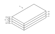
- a heat dissipation substrate 1 includes a first metal diamond composite layer 11, a second metal diamond composite layer 12, a first metal diamond composite layer 11, and a first metal diamond composite layer 11.
- Core material layer 10 disposed between two metal diamond composite layers 12, and the first metal diamond composite layer 11 and the second metal diamond composite layer 12 each have a diamond content of 50 volumes.
- the core material layer 10 has a thermal expansion coefficient in the direction parallel to the main surface of 4.5 ⁇ 10 ⁇ 6 K ⁇ 1 or more and 13 ⁇ 10 ⁇ 6 K ⁇ 1 or less, and heat conduction in the thickness direction.
- the rate is 140 W ⁇ m ⁇ 1 ⁇ K ⁇ 1 or more.
- the heat dissipation substrate 1 of the present embodiment includes the first metal diamond composite layer 11 and the second metal diamond composite layer 12 each having a diamond content of less than 50% by volume, the manufacturing cost is low and 400 W ⁇ m. It has a high thermal conductivity of -1 ⁇ K -1 or higher.
- the heat dissipation board 1 of the present embodiment has a thermal expansion coefficient in the direction parallel to the main surface of 4.5 ⁇ 10 ⁇ 6 K ⁇ 1 or more and 13 ⁇ 10 ⁇ 6 K ⁇ 1 or less and the thermal conductivity in the thickness direction. Includes a core material layer 10 having 140 W ⁇ m ⁇ 1 ⁇ K ⁇ 1 or more, and therefore has a thermal expansion coefficient that is the same as or close to that of the semiconductor element, and is suitable for mounting or holding a semiconductor element.
- the entire heat dissipation substrate 1 of the present embodiment has a thermal expansion coefficient in the direction parallel to the principal surface of 7 ⁇ 10 ⁇ 6 K ⁇ 1 or more and 13 ⁇ 10 ⁇ 6 K ⁇ 1 or less, and the heat conduction in the thickness direction thereof.
- the rate is preferably 400 W ⁇ m ⁇ 1 ⁇ K ⁇ 1 or more.
- the upper limit of the thickness direction of the thermal conductivity of the entire heat dissipating substrate 1 of this embodiment, at present, is about 600W ⁇ m -1 ⁇ K -1.
- the thermal expansion coefficient and thermal conductivity of the entire heat dissipation board 1 mean the thermal expansion coefficient and thermal conductivity when the entire heat dissipation board 1 is integrated.
- the heat dissipation substrate 1 having a thermal expansion coefficient and a thermal expansion coefficient within such a range has the same or approximate thermal expansion coefficient as that of the semiconductor element and has a high thermal conductivity. It is extremely suitable as a heat dissipation substrate for holding.
- the entire heat dissipation substrate 1 of the present embodiment preferably has a thickness T of 500 ⁇ m or more and 10000 ⁇ m or less. If the thickness T of the entire heat dissipation substrate 1 is less than 500 ⁇ m, the heat dissipation performance deteriorates. If the thickness T is greater than 10,000 ⁇ m, it is difficult to mount or hold semiconductor elements at a high density, making it suitable as a mounting substrate. Absent.
- the core material layer 10 of the heat dissipation substrate 1 of the present embodiment is disposed between the first metal diamond composite layer 11 and the second metal diamond composite layer 12.
- the first metal diamond composite layer 11 and the second metal diamond composite layer 12 have high thermal conductivity, but their thermal expansion coefficient is larger than the thermal expansion coefficient of the semiconductor element. Not suitable for mounting or holding elements. For this reason, the core material layer 10 is required to make the thermal expansion coefficient of the entire heat dissipation substrate 1 the same as or close to the thermal expansion coefficient of the semiconductor element.
- the core layer 10 has a thermal expansion coefficient in the direction parallel to the main surface of 4.5 ⁇ 10 ⁇ 6 K ⁇ 1 or more and 13 ⁇ 10 ⁇ 6 K ⁇ 1 or less, and heat conduction in the thickness direction.
- the rate needs to be 140 W ⁇ m ⁇ 1 ⁇ K ⁇ 1 or more.
- the upper limit of the thermal conductivity in the thickness direction of the core material layer 10 is currently about 250 W ⁇ m ⁇ 1 ⁇ K ⁇ 1 .
- the core material layer 10 is not particularly limited as long as it has the above-described thermal expansion coefficient and thermal conductivity, and may be a single layer composed of a single layer or a multilayer composed of a plurality of layers. Good.
- the single layer may be a single layer made of a single chemical species or a composite layer made of a plurality of chemical species.
- preferred examples of the single layer include a Mo layer, a W layer, an AlN layer, and a Si 3 N 4 layer.
- Preferred examples of the composite layer include a CuW layer and a CuMo layer.
- Mo / X / Mo layer (X is at least one selected from the group consisting of Cu, Ag, Cu diamond and Ag diamond), Mo / X / Mo / X / Mo layer (X is And at least one selected from the group consisting of Cu, Ag, Cu diamond and Ag diamond).
- the insulating core material layer 10 such as an AlN layer or a Si 3 N 4 layer is used, insulation can be imparted in the thickness direction of the heat dissipation substrate 1.
- the core material layer 10 is not particularly limited as long as it has the above-described thermal expansion coefficient and thermal conductivity, but preferably contains Mo, specifically, a Mo layer, a CuMo layer, Mo / X. / Mo layer (X is at least one selected from the group consisting of Cu, Ag, Cu diamond and Ag diamond), Mo / X / Mo / X / Mo layer (X is Cu, Ag, Cu diamond and Ag diamond) More preferably at least one selected from the group consisting of
- the core material layer 10 may have a metal layer formed on its surface by at least one of plating and vapor deposition.
- Suitable examples of the metal layer include a Ni layer, a Cu layer, an Ag layer, an Au layer, or a layer in which these layers are stacked.
- the thickness T 0 of the core material layer 10 is not particularly limited, but is preferably 50 ⁇ m or more and 4000 ⁇ m or less, and more preferably 250 ⁇ m or more and 1000 ⁇ m or less.
- the coefficient of thermal expansion in the direction parallel to the entire main surface of the heat dissipation board 1 is 7 ⁇ 10 ⁇ 6 K ⁇ 1 or more and 13 ⁇ 10 ⁇ 6 K ⁇ 1 or less. If the thickness T 0 of the core layer 10 is larger than 4000 ⁇ m, the thermal expansion coefficient in the thickness direction of the entire heat dissipation substrate 1 can be increased to 400 W ⁇ m ⁇ 1 ⁇ K ⁇ 1 or more. It becomes difficult.
- first metal diamond composite layer 11 is disposed on one main surface side of the core material layer 10
- the second metal diamond composite layer 12 is the other main surface of the core material layer 10. Arranged on the side. For this reason, the thermal radiation board
- the first metal diamond composite layer 11 and the second metal diamond composite layer 12 each have a diamond content of less than 50% by volume from the viewpoint of enabling punching by punching and reducing manufacturing costs. 40 volume% or less is preferable.
- first metal diamond composite layer 11 and the second metal diamond composite layer 12 have a thermal conductivity of 420 W ⁇ m ⁇ 1 ⁇ K ⁇ by setting the diamond content to 10% by volume or more. Can be as high as 1 or more.
- first metal diamond composite layer 11 and the second metal diamond composite layer 12 have a diamond content of less than 50% by volume, their respective thermal conductivities are 700 W ⁇ m ⁇ 1 ⁇ K ⁇ 1. Is less than.
- the core material layer 10 in the heat dissipation substrate 1 of the present embodiment has a thermal expansion coefficient of 4.5 ⁇ 10 ⁇ 6 K ⁇ 1 or more and 13 ⁇ 10 ⁇ 6 K ⁇ in a direction parallel to the main surface. 1 or less, and having a thermal expansion coefficient that is the same as or close to that of the semiconductor element, it is suitable for mounting or holding the semiconductor element.
- the thermal conductivity in the thickness direction is 140 W ⁇ m ⁇ 1.
- -K- 1 or more, and higher heat conductivity is desired as a heat dissipation board.
- the thermal conductivity in the thickness direction is 400 W ⁇ m ⁇ 1 ⁇ K ⁇ 1 or more.
- a heat dissipation substrate 1 having a high manufacturing cost and a low manufacturing cost can be obtained.
- the first metal diamond composite layer 11 and the second metal diamond composite layer 12 are layers formed of a composite containing a metal and diamond.
- a form in which diamond particles are dispersed in the metal have
- limiting in particular as a metal From a viewpoint with high heat conductivity, Cu, Ag, Al, etc. are used suitably. That is, a Cu diamond composite layer, an Ag diamond composite layer, an Al diamond composite layer, and the like are preferable.
- the particle size of the diamond particles is not particularly limited, but is preferably 20 ⁇ m or more from the viewpoint of improving workability, and is preferably 250 ⁇ m or less from the viewpoint of improving uniform dispersibility in the metal.
- first metal diamond composite layer 11 and the second metal diamond composite layer 12 may have a metal layer formed on at least one of the surfaces by plating and vapor deposition.
- Suitable examples of the metal layer include a Ni layer, a Cu layer, an Ag layer, an Au layer, or a layer in which these layers are stacked.
- the first metal diamond composite layer 11 and the second metal diamond composite layer 12 are required to have a diamond content of less than 50% by volume from the viewpoint of forming a high thermal conductivity layer at a low manufacturing cost. is there.
- the diamond content is 10% by volume or more and less than 50% by volume. It is preferable that it is 10 volume% or more and 40 volume% or less.
- the spray is not stable, and when the diamond content is higher than 50% by volume, bubbles are likely to be generated in the metal diamond composite layer during spraying.
- the diamond content of the first metal diamond composite layer 11 and the diamond content of the second metal diamond composite layer 12 may be the same or different.
- the thickness T 2 of the thickness T 1 and the second metal-diamond composite layer 12 of the first metal-diamond composite layer 11 may be different even in the same.
- the type and thickness T 0 of the core material layer 10 the diamond content and thickness T 1 of the first metal diamond composite layer 11, and the diamond content of the second metal diamond composite layer 12 and By changing the thickness T 2 , the heat dissipation substrate 1 having a desired thermal expansion coefficient and thermal conductivity can be obtained.
- the heat dissipation substrate 1 has, for example, the same diamond content of the first metal diamond composite layer 11 and the diamond content of the second metal diamond composite layer 12, and the first metal diamond composite. by the same thickness T 1 of the layer 11 and the thickness T 2 of the second metal-diamond composite layer 12, the parallel thermal expansion coefficient on the main surface a first metal-diamond composite layer 11 side and the second The same for the metal diamond composite layer 12 side.
- the diamond content of the first metal diamond composite layer 11 and the diamond content of the second metal diamond composite layer 12 are made different depending on the purpose of use, or the first metal diamond composite is used.
- the parallel thermal expansion coefficient on the main surface a first metal-diamond composite layer 11 side and the second It may be different on the metal diamond composite layer 12 side.
- the first metal diamond composite layer 11 and the second metal diamond composite layer 12 form a heat dissipation substrate 1 having a thermal expansion coefficient that is the same as or close to that of the semiconductor element and a high thermal conductivity.
- the thermal expansion coefficient in the direction parallel to each main surface is 8.5 ⁇ 10 ⁇ 6 K ⁇ 1 or more and 15 ⁇ 10 ⁇ 6 K ⁇ 1 or less, and the thermal conductivity in each thickness direction is 420 W ⁇ m. ⁇ 1 ⁇ K ⁇ 1 or more is preferable.
- the method for manufacturing the heat dissipation substrate of the present embodiment is not particularly limited.
- the step of preparing the core material layer 10 and the first main surface side of the core material layer 10 are the first.
- a step of forming the metal diamond composite layer 11 and forming the second metal diamond composite layer 12 on the other main surface side of the core material layer 10 can be included.
- the core material layer 10 to be prepared is as described above, and is not repeated here.
- the method for forming the first metal diamond composite layer 11 and the second metal diamond composite layer 12 is not particularly limited, and the first metal diamond composite layer 11 is directly formed on one main surface side of the core material layer 10.
- the first metal diamond composite layer 11 and the second metal diamond composite layer 12 are prepared in advance by a direct method of directly forming the second metal diamond composite layer 12 on the other main surface side of the core material layer 10.
- An indirect method in which the first metal diamond composite layer 11 is bonded to one main surface side of the core material layer 10 and the second metal diamond composite layer 12 is bonded to the other main surface side of the core material layer 10; and so on. From the viewpoint of efficiently forming the first metal diamond composite layer 11 and the second metal diamond composite layer 12 at a low production cost, a direct method is preferable.
- Direct method examples of the direct method include a spray method such as a cold spray method, an HVAF (High Velocity Aero Fuel) method, and an AD (Aerosol Deposition) method.
- a spray method such as a cold spray method, an HVAF (High Velocity Aero Fuel) method, and an AD (Aerosol Deposition) method.
- HVAF High Velocity Aero Fuel
- AD Anasol Deposition
- the spray method is not particularly limited.
- the heat radiation substrate is formed by spraying the metal diamond composition on the main surface side of both the sub-step of preparing the metal diamond composition for spraying and the core material layer. Obtaining sub-steps.
- a metal diamond composition for spraying is prepared.
- the metal diamond composition to be prepared is a powder of metal-coated diamond particles formed by coating a metal film on the surface of diamond particles, and the metal particle powder is added as necessary.
- the metal particle powder to be added is not particularly limited, Cu particle powder, Ag particle powder, Al particle powder and the like are preferable from the viewpoint of high thermal conductivity.
- the diamond content of the metal diamond composition is preferably 10% by volume or more and less than 50% by volume, more preferably 10% by volume or more and 40% by volume or less.
- the diamond content is lower than 10% by volume, the spray is not stable, and when the diamond content is higher than 50% by volume, bubbles are likely to be generated in the metal diamond composite layer during spraying.
- the particle diameter of diamond particles is not particularly limited, but is preferably 20 ⁇ m or more and 250 ⁇ m or less.
- the thickness of the metal film covered with the diamond particles is not particularly limited, but is preferably 1 ⁇ m or more and 30 ⁇ m or less. If the thickness of the metal film is less than 1 ⁇ m, the adhesion between the particles during spraying may be insufficient, and it is difficult to produce metal-coated diamond particles having a metal film thickness of more than 30 ⁇ m. Therefore, the particle diameter of the metal-coated diamond particles is not particularly limited, but is preferably 21 ⁇ m or more and 280 ⁇ m or less for the above reason.
- an intermediate metal film may be interposed between the diamond particles and the metal film.
- Such an intermediate metal film preferably contains at least one selected from the group consisting of Ti, V, Cr, Mn, Fe, Co, Ni and compounds containing these.
- the thickness of the intermediate metal film is not particularly limited, but is preferably 0.5 ⁇ m or more and 1.0 ⁇ m or less. If the thickness of the intermediate metal film is smaller than 0.5 ⁇ m, the heat conduction between the metal film and the diamond particles may be reduced. If the thickness of the intermediate metal film is larger than 1.0 ⁇ m, the intermediate metal film itself is heated. There is a risk of reducing the conductivity, and in any case, there is a risk of reducing the thermal conductivity of the metal diamond composite layer.
- the method for forming a metal film, or an intermediate metal film and a metal film on the surface of the diamond particles is not particularly limited, and is a plating method, a metal foil bonding method, a CVD (chemical vapor deposition) method.
- a CVD chemical vapor deposition
- Preferable examples include plasma CVD, MOCVD (metal organic chemical vapor deposition), vapor deposition, and spraying.
- metal diamond composition a powder of intermediate metal-coated diamond particles in which the above-described intermediate metal film is formed on diamond particles and a metal particle powder can also be used.
- the method for spraying the metal diamond composition is not particularly limited as long as it can form a metal diamond composite layer, and examples thereof include a cold spray method, an HVAF (High Velocity Aero Fuel) method, an AD (Aerosol Deposition) method, and the like. It is done.
- HVAF High Velocity Aero Fuel
- AD Alcohol Deposition
- the spraying conditions are not particularly limited as long as they are compatible with the metal diamond composition and the spraying method.
- spraying is performed using an inert gas such as nitrogen gas, helium gas, argon gas, or a mixed gas in which hydrogen gas is mixed with these inert gases.
- the gas pressure is 2 MPa or more and 5 MPa or less (more preferably 2 MPa or more and 4 MPa or less)
- the spraying gas temperature is 700 ° C. or more and 1000 ° C. or less (more preferably 700 ° C. or more and 900 ° C. or less)
- metal-coated diamond particles and
- the speed of the metal particles is preferably 700 m / s or more and 1000 m / s or less.
- the speed of the metal-coated diamond particles and the metal particles at the time of spraying is calculated by analyzing the image of the particles photographed by the CCD camera at the time of spraying.
- the manufacturing method of the heat dissipation substrate by the direct method it is preferable to further include a sub-process of heat-treating the obtained heat dissipation substrate 1 from the viewpoint of removing the oxide in the heat dissipation substrate and improving the bonding force between the particles.
- the heat treatment atmosphere is a non-oxidizing atmosphere containing a reducing gas, for example, a hydrogen gas atmosphere, a hydrogen gas, from the viewpoint of removing oxides in the heat dissipation substrate formed during spraying.
- a mixed gas atmosphere of nitrogen gas and the like is preferable.
- the heat treatment temperature is preferably 400 ° C. or more and 600 ° C. or less from the viewpoint of removing oxides in the heat dissipation substrate and improving the bonding force between the particles.
- the heat treatment time is preferably 0.2 hours or more and 1 hour or less from the viewpoint of removing the oxide in the heat dissipation substrate and improving the bonding force between the particles.
- the indirect method is not particularly limited, but for example, a first metal diamond wafer (first metal diamond composite layer 11) and a second metal diamond wafer (second metal diamond composite layer 12) are formed.
- a first metal diamond wafer (first metal diamond composite layer 11) and a second metal diamond wafer (second metal diamond composite layer 12) are respectively provided on the main surface side of both the sub-process and the core material layer 10. And a sub-process of obtaining a heat dissipation substrate by bonding.
- the method for forming the first metal diamond wafer (first metal diamond composite layer 11) and the second metal diamond wafer (second metal diamond composite layer 12) is not particularly limited, and is a sintering method or infiltration. Suitable examples include a method, an HP (hot press) method, an electric current sintering method, and a rolling method.
- the first metal diamond wafer (first metal diamond composite layer 11) and the second metal diamond wafer (second metal diamond composite layer 12) to be formed are formed of a composite containing a metal and diamond.
- it has a form in which diamond particles are dispersed in a metal.
- a metal From a viewpoint with high heat conductivity, Cu, Ag, Al, etc. are used suitably. That is, a Cu diamond composite wafer, an Ag diamond composite wafer, an Al diamond composite wafer, and the like are preferable.
- the particle size of the diamond particles is not particularly limited, but is preferably 20 ⁇ m or more from the viewpoint of improving workability, and is preferably 250 ⁇ m or less from the viewpoint of improving uniform dispersibility in the metal.
- the first metal diamond wafer (first metal diamond composite layer 11) and the second metal diamond wafer (second metal diamond composite layer 12) are a first metal diamond composite layer having a low manufacturing cost and high thermal conductivity.
- the diamond content is preferably 10% by volume or more and less than 50% by volume, and preferably 10% by volume or more and 40% by volume or less. More preferred. If the diamond content is lower than 10% by volume, a wafer having a high thermal conductivity cannot be obtained, and if the diamond content is higher than 50% by volume, a high pressure is required for manufacturing the wafer, resulting in an increase in manufacturing cost.
- the diamond content of the first metal diamond wafer (first metal diamond composite layer 11) and the diamond content of the second metal diamond wafer (second metal diamond composite layer 12) are the same. May be different.
- the diamond content of the first metal diamond wafer (first metal diamond composite layer 11) and the metal diamond composition that is a raw material for forming the second metal diamond wafer are not particularly limited. From the viewpoint of high workability and formability, the metal diamond composition used in the direct method is preferred.
- the thickness T 2 of the first metal-diamond wafer (first metal-diamond composite layer 11) thickness T 1 and the second metal diamond wafer (second metal-diamond composite layer 12) is the same Or different.
- a first metal diamond wafer (first metal diamond composite layer 11) is bonded to one main surface side of the core material layer 10, and a second metal diamond is bonded to the other main surface side of the core material layer 10.
- a wafer (second metal diamond composite layer 12) is bonded together. In this way, the heat dissipation substrate 1 in which the core material layer 10 is disposed between the first metal diamond composite layer 11 and the second metal diamond composite layer 12 is obtained.
- the method for bonding the first metal diamond wafer (first metal diamond composite layer 11) and the second metal diamond wafer (second metal diamond composite layer 12) to the core material layer 10 is not particularly limited.
- Preferable methods include an attaching method, an HP method, a rolling method, an electric current sintering method, and a combination thereof.
- Example 1 (Example 1-1) 1.
- core material layer 10 Mo having a diameter of 2 inches (5.08 cm) and a thickness of 500 ⁇ m (Mo purity is 99.9% by mass)
- Cu diamond composition (metal diamond composition) is applied by cold spraying on the main surfaces on both sides of the Mo core material (core material layer 10).
- a Cu diamond composition As a Cu diamond composition (metal diamond composition), a commercially available Ti coating in which a Ti layer having a thickness of 0.5 ⁇ m to 1.0 ⁇ m is coated on diamond particles having an average particle diameter of 100 ⁇ m and a purity of 99.9% by mass Powder of Cu / Ti coated diamond particles (metal coated diamond particles) in which an electroless plating Cu layer having a thickness of 10 ⁇ m is formed on diamond particles (MBG600 100 ⁇ TI manufactured by DI (Diamond Innovation International)) and electrolysis having an average particle diameter of 100 ⁇ m What mixed the powder of Cu (metal) particle
- a first Cu diamond composite layer having a thickness of 600 ⁇ m is obtained by cold spraying the Cu diamond composition (metal diamond composition) on one and other main surfaces of the Mo core material (core material layer 10).
- a (first metal diamond composite layer 11) and a second Cu diamond composite layer (second metal diamond composite layer 12) having a thickness of 600 ⁇ m were formed.
- the Mo core material (core material layer 10) is provided between the first Cu diamond composite layer (first metal diamond composite layer 11) and the second Cu diamond composite layer (second metal diamond composite layer 12).
- a Cu diamond composition metal diamond composition
- nitrogen gas is used as a spray gas
- the spray gas pressure is 4 MPa
- the spray gas temperature is 800 ° C.
- the speed of coated diamond particles) and Cu particles (metal particles) was 800 m / s.
- thermal conductivity ⁇ 200 W ⁇ m ⁇ 1 ⁇ K ⁇ 1
- thermal conductivity ⁇ 200 W ⁇ m ⁇ 1 ⁇ K ⁇ 1
- the thermal conductivity ⁇ in the thickness direction of the heat radiating substrate 1 is 408 W ⁇ m ⁇ 1 ⁇ K ⁇ 1 as measured by a laser flash method on a 10 mm diameter sample cut out from the heat radiating substrate and having a thickness of 1700 ⁇ m. It was extremely expensive.
- the bonding strength between the Cu diamond composite layer (metal diamond composite layer) and the Mo core material (core material layer) is 2 inches (5.08 cm) in diameter with the Cu diamond composite layer (metal diamond composite layer) and the Mo core material.
- Example 1-2 Heat dissipation similar to Example 1-1, except that the thickness of the core layer was 300 ⁇ m, the particle size of diamond particles in the first and second metal diamond composite layers was 250 ⁇ m, and the diamond content was 8% by volume. A substrate was produced.
- the obtained heat dissipation board has a thickness of 1500 ⁇ m, a thermal expansion coefficient ⁇ of 14.2 ⁇ 10 ⁇ 6 K ⁇ 1 and is suitable for mounting or holding a semiconductor element, and a thermal conductivity ⁇ of 390 W ⁇ m ⁇ . as high as 1 ⁇ K -1, the bonding strength between the metal-diamond composite layer and the core layer was extremely large as 0.69GPa.
- Example 1-2 since the diamond content was lower than the preferred range, the thermal expansion coefficient ⁇ of the heat dissipation substrate was higher than the preferred range, and the thermal conductivity ⁇ of the heat dissipation substrate was lower than the preferred range. .
- Table 1 The results are summarized in Table 1.
- Example 1-3 A heat radiating substrate similar to Example 1-2 was prepared except that the diamond content in the first and second metal diamond composite layers was 10% by volume.
- the obtained heat dissipation board has a thickness of 1500 ⁇ m, a thermal expansion coefficient ⁇ of 13.0 ⁇ 10 ⁇ 6 K ⁇ 1 , suitable for mounting or holding a semiconductor element, and a thermal conductivity ⁇ of 409 W ⁇ m ⁇ . extremely high and 1 ⁇ K -1, the bonding strength between the metal-diamond composite layer and the core layer was extremely large as 0.60GPa.
- Table 1 The results are summarized in Table 1.
- Example 1-4 A heat dissipation substrate was produced in the same manner as in Example 1-2 except that the diamond content in the first and second metal diamond composite layers was 20% by volume.
- the obtained heat dissipation substrate has a thickness of 1500 ⁇ m, a thermal expansion coefficient ⁇ of 11.4 ⁇ 10 ⁇ 6 K ⁇ 1 and is suitable for mounting or holding a semiconductor element, and a thermal conductivity ⁇ of 441 W ⁇ m ⁇ . extremely high and 1 ⁇ K -1, the bonding strength between the metal-diamond composite layer and the core layer was extremely large as 0.57GPa.
- Table 1 The results are summarized in Table 1.
- Example 1-5 A heat dissipation substrate was produced in the same manner as in Example 1-2 except that the diamond content in the first and second metal diamond composite layers was 30% by volume.
- the obtained heat dissipation board has a thickness of 1500 ⁇ m, a thermal expansion coefficient ⁇ of 8.5 ⁇ 10 ⁇ 6 K ⁇ 1 and is suitable for mounting or holding a semiconductor element, and a thermal conductivity ⁇ of 478 W ⁇ m ⁇ . extremely high and 1 ⁇ K -1, the bonding strength between the metal-diamond composite layer and the core layer was extremely large as 0.56GPa.
- Table 1 The results are summarized in Table 1.
- Example 1-6 A heat radiating substrate similar to Example 1-2 was prepared except that the diamond content in the first and second metal diamond composite layers was 40% by volume.
- the obtained heat dissipation board has a thickness of 1500 ⁇ m, a thermal expansion coefficient ⁇ of 8.1 ⁇ 10 ⁇ 6 K ⁇ 1 and is suitable for mounting or holding a semiconductor element, and a thermal conductivity ⁇ of 521 W ⁇ m ⁇ . extremely high and 1 ⁇ K -1, the bonding strength between the metal-diamond composite layer and the core layer was extremely large as 0.56GPa.
- Table 1 The results are summarized in Table 1.
- Example 1--7 A heat radiating substrate similar to Example 1-2 was prepared except that the diamond content in the first and second metal diamond composite layers was 50% by volume.
- the obtained heat dissipation board has a thickness of 1500 ⁇ m, a thermal expansion coefficient ⁇ of 7.2 ⁇ 10 ⁇ 6 K ⁇ 1 and is suitable for mounting or holding a semiconductor element, and a thermal conductivity ⁇ of 374 W ⁇ m ⁇ . 1 ⁇ K ⁇ 1 , and the bonding strength between the metal diamond composite layer and the core material layer was as extremely high as 0.57 GPa.
- Example 1-7 since the diamond content was too high, the thermal conductivity ⁇ of the heat dissipation substrate was low. The results are summarized in Table 1.
- Example 1-8 A heat dissipation substrate was produced in the same manner as in Example 1-7, except that the diamond particle size in the first and second metal diamond composite layers was 300 ⁇ m.
- the obtained heat dissipation board has a thickness of 1500 ⁇ m, a thermal expansion coefficient ⁇ of 6.8 ⁇ 10 ⁇ 6 K ⁇ 1 and is suitable for mounting or holding a semiconductor element, and a thermal conductivity ⁇ of 320 W ⁇ m ⁇ . It was 1 ⁇ K ⁇ 1 , and the bonding strength between the metal diamond composite layer and the core material layer was as extremely high as 0.56 GPa.
- Example 1-8 since the diamond content was too high and the particle size of the diamond particles was higher than the preferred range, the thermal expansion coefficient ⁇ of the heat radiating substrate was lower than the preferred range, The conductivity ⁇ was lowered.
- Table 1 The results are summarized in Table 1.
- Example 1-9 A heat dissipating substrate similar to Example 1-5 was prepared except that the particle diameter of diamond particles in the first and second metal diamond composite layers was 100 ⁇ m.
- the obtained heat dissipation board has a thickness of 1500 ⁇ m, a thermal expansion coefficient ⁇ of 8.5 ⁇ 10 ⁇ 6 K ⁇ 1 and is suitable for mounting or holding a semiconductor element, and a thermal conductivity ⁇ of 437 W ⁇ m ⁇ . extremely high and 1 ⁇ K -1, the bonding strength between the metal-diamond composite layer and the core layer was extremely large as 0.56GPa.
- Table 1 The results are summarized in Table 1.
- Example 1-10 A heat dissipation substrate was produced in the same manner as in Example 1-5, except that the diamond particle size in the first and second metal diamond composite layers was 20 ⁇ m.
- the obtained heat dissipation board has a thickness of 1500 ⁇ m, a thermal expansion coefficient ⁇ of 8.5 ⁇ 10 ⁇ 6 K ⁇ 1 and is suitable for mounting or holding a semiconductor element, and a thermal conductivity ⁇ of 405 W ⁇ m ⁇ . extremely high and 1 ⁇ K -1, the bonding strength between the metal-diamond composite layer and the core layer was extremely large as 0.56GPa.
- Table 1 The results are summarized in Table 1.
- Example 1-11 A heat dissipating substrate similar to Example 1-5 was prepared except that the particle diameter of the diamond particles in the first and second metal diamond composite layers was 15 ⁇ m.
- the obtained heat dissipation substrate has a thickness of 1500 ⁇ m, a thermal expansion coefficient ⁇ of 8.5 ⁇ 10 ⁇ 6 K ⁇ 1 and is suitable for mounting or holding a semiconductor element, and a thermal conductivity ⁇ of 397 W ⁇ m ⁇ . as high as 1 ⁇ K -1, the bonding strength between the metal-diamond composite layer and the core layer was extremely large as 0.56GPa.
- the particle size of the diamond particles was lower than the preferred range, so the thermal conductivity ⁇ of the heat dissipation substrate was lower than the preferred range.
- Table 1 The results are summarized in Table 1.
- Example 1-12 The thickness of the core layer is 100 ⁇ m, the thickness of the first and second metal diamond composite layers is 100 ⁇ m, and the particle diameter of the diamond particles in the first and second metal diamond composite layers is 50 ⁇ m.
- a heat dissipation substrate similar to that in Example 1-5 was produced.
- the obtained heat dissipation substrate has a thickness of 300 ⁇ m, a thermal expansion coefficient ⁇ of 8.5 ⁇ 10 ⁇ 6 K ⁇ 1 and is suitable for mounting or holding a semiconductor element, and a thermal conductivity ⁇ of 402 W ⁇ m ⁇ .
- extremely high and 1 ⁇ K -1 the bonding strength between the metal-diamond composite layer and the core layer was extremely large as 0.56GPa.
- Table 1 The results are summarized in Table 1.
- Example 1-13 A heat radiating substrate was produced in the same manner as in Example 1-12 except that the thickness of the core layer was 250 ⁇ m and the thickness of the first and second metal diamond composite layers was 250 ⁇ m.
- the obtained heat dissipation substrate has a thickness of 750 ⁇ m, a thermal expansion coefficient ⁇ of 8.5 ⁇ 10 ⁇ 6 K ⁇ 1 and is suitable for mounting or holding a semiconductor element, and a thermal conductivity ⁇ of 405 W ⁇ m ⁇ . extremely high and 1 ⁇ K -1, the bonding strength between the metal-diamond composite layer and the core layer was extremely large as 0.56GPa.
- Table 1 The results are summarized in Table 1.
- Example 1-14 A heat radiating substrate was produced in the same manner as in Example 1-12 except that the thickness of the core material layer was 1000 ⁇ m and the thickness of the first and second metal diamond composite layers was 1000 ⁇ m.
- the obtained heat dissipation board has a thickness of 3000 ⁇ m, a thermal expansion coefficient ⁇ of 8.5 ⁇ 10 ⁇ 6 K ⁇ 1 and is suitable for mounting or holding a semiconductor element, and a thermal conductivity ⁇ of 410 W ⁇ m ⁇ . extremely high and 1 ⁇ K -1, the bonding strength between the metal-diamond composite layer and the core layer was extremely large as 0.57GPa.
- Table 1 The results are summarized in Table 1.
- Example 1-15 A heat dissipation substrate was produced in the same manner as in Example 1-14 except that the thickness of the first and second metal diamond composite layers was 2000 ⁇ m.
- the obtained heat dissipation substrate has a thickness of 5000 ⁇ m, a thermal expansion coefficient ⁇ of 8.5 ⁇ 10 ⁇ 6 K ⁇ 1 and is suitable for mounting or holding a semiconductor element, and a thermal conductivity ⁇ of 471 W ⁇ m ⁇ . extremely high and 1 ⁇ K -1, the bonding strength between the metal-diamond composite layer and the core layer was extremely large as 0.56GPa.
- Table 1 The results are summarized in Table 1.
- Example 1-16 A core material layer having a diameter of 2 inches (5.08 cm) and a thickness of 600 ⁇ m is W (W purity is 99.9% by mass).
- Core material coefficient of thermal expansion ⁇ : 4.5 ⁇ 10 ⁇ 6 K ⁇ 1
- a heat radiating substrate was produced in the same manner as in Example 1-9 except that the thermal conductivity ⁇ was 180 W ⁇ m ⁇ 1 ⁇ K ⁇ 1 ).
- the obtained heat dissipation substrate has a thickness of 1800 ⁇ m, a thermal expansion coefficient ⁇ of 8.3 ⁇ 10 ⁇ 6 K ⁇ 1 and is suitable for mounting or holding a semiconductor element, and a thermal conductivity ⁇ of 444 W ⁇ m ⁇ . extremely high and 1 ⁇ K -1, the bonding strength between the metal-diamond composite layer and the core layer was extremely large as 0.66GPa.
- Table 1 The results are summarized in Table 1.
- the core material layer has a diameter of 2 inches (5.08 cm) and a thickness of 600 ⁇ m MoCu (Mo: 60 mass%, Cu: 40 mass%, the purity of Mo and Cu is 99.9 mass%, respectively)
- a heat dissipation substrate was prepared in the same manner as in Example 1-9 except that the expansion coefficient ⁇ was 11 ⁇ 10 ⁇ 6 K ⁇ 1 and the thermal conductivity ⁇ was 234 W ⁇ m ⁇ 1 ⁇ K ⁇ 1 ).
- the obtained heat dissipation substrate has a thickness of 1800 ⁇ m, a thermal expansion coefficient ⁇ of 10.2 ⁇ 10 ⁇ 6 K ⁇ 1 and is suitable for mounting or holding a semiconductor element, and a thermal conductivity ⁇ of 477 W ⁇ m ⁇ . extremely high and 1 ⁇ K -1, the bonding strength between the metal-diamond composite layer and the core layer was extremely large as 0.48GPa.
- Table 1 The results are summarized in Table 1.
- Example 1-18 WNi having a diameter of 2 inches (5.08 cm) and a thickness of 600 ⁇ m (W: 99% by mass, Ni: 1% by mass, purity of W and Ni are each 99.9% by mass)
- a heat dissipation board was produced in the same manner as in Example 1-9 except that the expansion coefficient ⁇ was 5 ⁇ 10 ⁇ 6 K ⁇ 1 and the thermal conductivity ⁇ was 130 W ⁇ m ⁇ 1 ⁇ K ⁇ 1 .
- the substrate has a thickness of 1800 ⁇ m, a thermal expansion coefficient ⁇ of 8.1 ⁇ 10 ⁇ 6 K ⁇ 1 and is suitable for mounting or holding a semiconductor element, and a thermal conductivity ⁇ of 395 W ⁇ m ⁇ 1 ⁇ K ⁇ .
- the core material layer has a diameter of 2 inches (5.08 cm) and a thickness of 600 ⁇ m MoCu (Mo: 20 mass%, Cu: 80 mass%, the purity of Mo and Cu is 99.9 mass%, respectively)
- a heat dissipation substrate was prepared in the same manner as in Example 1-9 except that the expansion coefficient ⁇ was 16 ⁇ 10 ⁇ 6 K ⁇ 1 and the thermal conductivity ⁇ was 340 W ⁇ m ⁇ 1 ⁇ K ⁇ 1 ).
- the obtained heat dissipation substrate has a thickness of 1800 ⁇ m, a thermal expansion coefficient ⁇ of 13.5 ⁇ 10 ⁇ 6 K ⁇ 1 and is suitable for mounting or holding a semiconductor element, and a thermal conductivity ⁇ of 517 W ⁇ m ⁇ . extremely high and 1 ⁇ K -1, the bonding strength between the metal-diamond composite layer and the core layer was extremely large as 0.54GPa. In Example 1-19, since the thermal expansion coefficient ⁇ of the core material layer was too high, the thermal expansion coefficient ⁇ of the heat dissipation board was increased. The results are summarized in Table 1.
- Example 2 (Example 2-1) 1.
- core material layer 10 Mo having a diameter of 2 inches (5.08 cm) and a thickness of 500 ⁇ m (Mo purity is 99.9% by mass)
- Example 1-1 of Example 1 An electroless plated Cu layer with a thickness of 10 ⁇ m is formed on commercially available Ti-coated diamond particles (MBG600 100 ⁇ TI manufactured by DI (Diamond Innovation International) Co., Ltd.) in which a Ti layer with a thickness of 0.5 ⁇ m to 1.0 ⁇ m is coated on each diamond particle.
- MSG600 100 ⁇ TI manufactured by DI (Diamond Innovation International) Co., Ltd.
- a Ti layer with a thickness of 0.5 ⁇ m to 1.0 ⁇ m is coated on each diamond particle.
- the Cu diamond composition was embossed at a pressure of 8000 kgf / cm 2 , sintered in a vacuum atmosphere at 850 ° C. for 2 hours, and then hot-rolled at 630 ° C. under a reduction ratio of 10%.
- first and second metal diamond composite layers each having a thickness of 600 ⁇ m were obtained.
- Example 2-2 The heat dissipation was the same as in Example 2-1, except that the thickness of the core layer was 300 ⁇ m, the particle size of diamond particles in the first and second metal diamond composite layers was 250 ⁇ m, and the diamond content was 8% by volume.
- a substrate was produced.
- the obtained heat dissipation substrate has a thickness of 1500 ⁇ m, a thermal expansion coefficient ⁇ of 14.0 ⁇ 10 ⁇ 6 K ⁇ 1 and is suitable for mounting or holding a semiconductor element, and a thermal conductivity ⁇ of 387 W ⁇ m ⁇ . as high as 1 ⁇ K -1, the bonding strength between the metal-diamond composite layer and the core layer was extremely large as 0.67GPa.
- Example 2-2 since the diamond content was lower than the preferred range, the thermal expansion coefficient ⁇ of the heat dissipation substrate was higher than the preferred range, and the thermal conductivity ⁇ of the heat dissipation substrate was lower than the preferred range. .
- Table 2 The results are summarized in Table 2.
- Example 2-3 A heat dissipation substrate was produced in the same manner as in Example 2-2 except that the diamond content in the first and second metal diamond composite layers was 10% by volume.
- the obtained heat dissipation board has a thickness of 1500 ⁇ m, a thermal expansion coefficient ⁇ of 12.9 ⁇ 10 ⁇ 6 K ⁇ 1 and is suitable for mounting or holding a semiconductor element, and a thermal conductivity ⁇ of 408 W ⁇ m ⁇ . extremely high and 1 ⁇ K -1, the bonding strength between the metal-diamond composite layer and the core layer was extremely large as 0.61GPa.
- Table 2 The results are summarized in Table 2.
- Example 2-4 A heat dissipation substrate was produced in the same manner as in Example 2-2 except that the diamond content in the first and second metal diamond composite layers was 20% by volume.
- the obtained heat dissipation substrate has a thickness of 1500 ⁇ m, a thermal expansion coefficient ⁇ of 11.0 ⁇ 10 ⁇ 6 K ⁇ 1 and is suitable for mounting or holding a semiconductor element, and a thermal conductivity ⁇ of 451 W ⁇ m ⁇ . extremely high and 1 ⁇ K -1, the bonding strength between the metal-diamond composite layer and the core layer was extremely large as 0.56GPa.
- Table 2 The results are summarized in Table 2.
- Example 2-5 A heat radiating substrate similar to Example 2-2 was prepared except that the diamond content in the first and second metal diamond composite layers was 30% by volume.
- the obtained heat dissipation board has a thickness of 1500 ⁇ m, a thermal expansion coefficient ⁇ of 8.3 ⁇ 10 ⁇ 6 K ⁇ 1 and is suitable for mounting or holding a semiconductor element, and a thermal conductivity ⁇ of 480 W ⁇ m ⁇ . extremely high and 1 ⁇ K -1, the bonding strength between the metal-diamond composite layer and the core layer was extremely large as 0.56GPa.
- Table 2 The results are summarized in Table 2.
- Example 2-6 A heat dissipation substrate was produced in the same manner as in Example 2-2 except that the diamond content in the first and second metal diamond composite layers was 40% by volume.
- the obtained heat dissipation substrate has a thickness of 1500 ⁇ m, a thermal expansion coefficient ⁇ of 8.2 ⁇ 10 ⁇ 6 K ⁇ 1 and is suitable for mounting or holding a semiconductor element, and a thermal conductivity ⁇ of 520 W ⁇ m ⁇ . extremely high and 1 ⁇ K -1, the bonding strength between the metal-diamond composite layer and the core layer was extremely large as 0.59GPa.
- Table 2 The results are summarized in Table 2.
- Example 2--7 A heat radiating substrate similar to Example 2-2 was prepared except that the diamond content in the first and second metal diamond composite layers was 50% by volume.
- the obtained heat dissipation board has a thickness of 1500 ⁇ m, a thermal expansion coefficient ⁇ of 7.4 ⁇ 10 ⁇ 6 K ⁇ 1 and is suitable for mounting or holding a semiconductor element, and a thermal conductivity ⁇ of 377 W ⁇ m ⁇ . 1 ⁇ K ⁇ 1 , and the bonding strength between the metal diamond composite layer and the core material layer was as extremely high as 0.55 GPa.
- Example 2-7 since the diamond content was too high, the thermal conductivity ⁇ of the heat dissipation substrate was low. The results are summarized in Table 2.
- Example 2-8 A heat dissipation substrate was produced in the same manner as in Example 2-7, except that the diamond particle size in the first and second metallic diamond composite layers was 300 ⁇ m.
- the obtained heat dissipation board has a thickness of 1500 ⁇ m, a thermal expansion coefficient ⁇ of 6.8 ⁇ 10 ⁇ 6 K ⁇ 1 and is suitable for mounting or holding a semiconductor element, and a thermal conductivity ⁇ of 321 W ⁇ m ⁇ . 1 ⁇ K ⁇ 1 , and the bonding strength between the metal diamond composite layer and the core material layer was as extremely high as 0.55 GPa.
- Example 2-8 because the diamond content was too high and the particle size of the diamond particles was higher than the preferred range, the thermal expansion coefficient ⁇ of the heat radiating substrate was lower than the preferred range, The conductivity ⁇ was lowered.
- Table 2 The results are summarized in Table 2.
- Example 2-9 A heat dissipation substrate was produced in the same manner as in Example 2-5, except that the diamond particle size in the first and second metal diamond composite layers was 100 ⁇ m.
- the obtained heat dissipation board has a thickness of 1500 ⁇ m, a thermal expansion coefficient ⁇ of 8.4 ⁇ 10 ⁇ 6 K ⁇ 1 and is suitable for mounting or holding a semiconductor element, and a thermal conductivity ⁇ of 440 W ⁇ m ⁇ . extremely high and 1 ⁇ K -1, the bonding strength between the metal-diamond composite layer and the core layer was extremely large as 0.58GPa.
- Table 2 The results are summarized in Table 2.
- Example 2-10 A heat dissipation substrate was produced in the same manner as in Example 2-5, except that the diamond particle size in the first and second metal diamond composite layers was 20 ⁇ m.
- the obtained heat dissipation board has a thickness of 1500 ⁇ m, a thermal expansion coefficient ⁇ of 8.2 ⁇ 10 ⁇ 6 K ⁇ 1 and is suitable for mounting or holding a semiconductor element, and a thermal conductivity ⁇ of 415 W ⁇ m ⁇ . extremely high and 1 ⁇ K -1, the bonding strength between the metal-diamond composite layer and the core layer was extremely large as 0.54GPa.
- Table 2 The results are summarized in Table 2.
- Example 2-11 A heat dissipation substrate was produced in the same manner as in Example 2-5, except that the diamond particle size in the first and second metal diamond composite layers was 15 ⁇ m.
- the obtained heat dissipation substrate has a thickness of 1500 ⁇ m, a thermal expansion coefficient ⁇ of 8.3 ⁇ 10 ⁇ 6 K ⁇ 1 and is suitable for mounting or holding a semiconductor element, and a thermal conductivity ⁇ of 397 W ⁇ m ⁇ . as high as 1 ⁇ K -1, the bonding strength between the metal-diamond composite layer and the core layer was extremely large as 0.55GPa.
- the particle size of the diamond particles was lower than the preferred range, so the thermal conductivity ⁇ of the heat dissipation substrate was lower than the preferred range.
- Table 2 The results are summarized in Table 2.
- Example 2-12 The thickness of the core layer is 100 ⁇ m, the thickness of the first and second metal diamond composite layers is 100 ⁇ m, and the particle diameter of the diamond particles in the first and second metal diamond composite layers is 50 ⁇ m.
- a heat dissipation substrate similar to that in Example 2-5 was produced.
- the obtained heat dissipation substrate has a thickness of 300 ⁇ m, a thermal expansion coefficient ⁇ of 8.5 ⁇ 10 ⁇ 6 K ⁇ 1 and is suitable for mounting or holding a semiconductor element, and a thermal conductivity ⁇ of 409 W ⁇ m ⁇ .
- extremely high and 1 ⁇ K -1 the bonding strength between the metal-diamond composite layer and the core layer was extremely large as 0.55GPa.
- Table 2 The results are summarized in Table 2.
- Example 2-13 A heat radiating substrate was produced in the same manner as in Example 2-12 except that the thickness of the core layer was 250 ⁇ m and the thickness of the first and second metal diamond composite layers was 250 ⁇ m.
- the obtained heat dissipation substrate has a thickness of 750 ⁇ m, a thermal expansion coefficient ⁇ of 8.4 ⁇ 10 ⁇ 6 K ⁇ 1 and is suitable for mounting or holding a semiconductor element, and a thermal conductivity ⁇ of 404 W ⁇ m ⁇ . extremely high and 1 ⁇ K -1, the bonding strength between the metal-diamond composite layer and the core layer was extremely large as 0.56GPa.
- Table 2 The results are summarized in Table 2.
- Example 2-14 A heat dissipation substrate was produced in the same manner as in Example 2-12 except that the thickness of the core material layer was 1000 ⁇ m and the thickness of the first and second metal diamond composite layers was 1000 ⁇ m.
- the obtained heat dissipation substrate has a thickness of 3000 ⁇ m, a thermal expansion coefficient ⁇ of 8.6 ⁇ 10 ⁇ 6 K ⁇ 1 and is suitable for mounting or holding a semiconductor element, and a thermal conductivity ⁇ of 411 W ⁇ m ⁇ . extremely high and 1 ⁇ K -1, the bonding strength between the metal-diamond composite layer and the core layer was extremely high as 0.57GPa.
- Table 2 The results are summarized in Table 2.
- Example 2-15 A heat dissipation substrate was produced in the same manner as in Example 2-14 except that the thickness of the first and second metal diamond composite layers was 2000 ⁇ m.
- the obtained heat dissipation substrate has a thickness of 5000 ⁇ m, a thermal expansion coefficient ⁇ of 8.3 ⁇ 10 ⁇ 6 K ⁇ 1 and is suitable for mounting or holding a semiconductor element, and a thermal conductivity ⁇ of 481 W ⁇ m ⁇ . extremely high and 1 ⁇ K -1, the bonding strength between the metal-diamond composite layer and the core layer was extremely large as 0.57GPa.
- Table 2 The results are summarized in Table 2.
- Example 2-16 A core material layer having a diameter of 2 inches (5.08 cm) and a thickness of 600 ⁇ m is W (W purity is 99.9% by mass).
- Core material coefficient of thermal expansion ⁇ : 4.5 ⁇ 10 ⁇ 6 K ⁇ 1
- a heat dissipation substrate was produced in the same manner as in Example 2-9 except that the thermal conductivity ⁇ was 180 W ⁇ m ⁇ 1 ⁇ K ⁇ 1 ).
- the obtained heat dissipation substrate has a thickness of 1800 ⁇ m, a thermal expansion coefficient ⁇ of 8.9 ⁇ 10 ⁇ 6 K ⁇ 1 , suitable for mounting or holding a semiconductor element, and a thermal conductivity ⁇ of 454 W ⁇ m ⁇ . extremely high and 1 ⁇ K -1, the bonding strength between the metal-diamond composite layer and the core layer was extremely large as 0.65GPa.
- Table 2 The results are summarized in Table 2.
- Example 2-1-7 The core material layer has a diameter of 2 inches (5.08 cm) and a thickness of 600 ⁇ m MoCu (Mo: 60 mass%, Cu: 40 mass%, the purity of Mo and Cu is 99.9 mass%, respectively)
- a heat dissipation substrate was prepared in the same manner as in Example 2-9 except that the expansion coefficient ⁇ was 11 ⁇ 10 ⁇ 6 K ⁇ 1 and the thermal conductivity ⁇ was 234 W ⁇ m ⁇ 1 ⁇ K ⁇ 1 ).
- the obtained heat dissipation board has a thickness of 1800 ⁇ m, a thermal expansion coefficient ⁇ of 10.0 ⁇ 10 ⁇ 6 K ⁇ 1 and is suitable for mounting or holding a semiconductor element, and a thermal conductivity ⁇ of 480 W ⁇ m ⁇ . extremely high and 1 ⁇ K -1, the bonding strength between the metal-diamond composite layer and the core layer was extremely large as 0.49 GPa.
- Table 2 The results are summarized in Table 2.
- Example 2-18 WNi having a diameter of 2 inches (5.08 cm) and a thickness of 600 ⁇ m (W: 99% by mass, Ni: 1% by mass, purity of W and Ni are each 99.9% by mass)
- a heat dissipation substrate was produced in the same manner as in Example 2-9 except that the expansion coefficient ⁇ was 5 ⁇ 10 ⁇ 6 K ⁇ 1 and the thermal conductivity ⁇ was 130 W ⁇ m ⁇ 1 ⁇ K ⁇ 1 ).
- the obtained heat dissipation substrate has a thickness of 1800 ⁇ m, a thermal expansion coefficient ⁇ of 8.3 ⁇ 10 ⁇ 6 K ⁇ 1 , suitable for mounting or holding a semiconductor element, and a thermal conductivity ⁇ of 391 W ⁇ m ⁇ .
- Example 2-18 since the thermal conductivity ⁇ of the core layer was too low, the thermal conductivity ⁇ of the heat dissipation substrate was low. The results are summarized in Table 2.
- the core material layer has a diameter of 2 inches (5.08 cm) and a thickness of 600 ⁇ m MoCu (Mo: 20 mass%, Cu: 80 mass%, the purity of Mo and Cu is 99.9 mass%, respectively)
- a heat dissipation substrate was prepared in the same manner as in Example 2-9 except that the expansion coefficient ⁇ was 16 ⁇ 10 ⁇ 6 K ⁇ 1 and the thermal conductivity ⁇ was 340 W ⁇ m ⁇ 1 ⁇ K ⁇ 1 ).
- the obtained heat dissipation substrate has a thickness of 1800 ⁇ m, a thermal expansion coefficient ⁇ of 13.2 ⁇ 10 ⁇ 6 K ⁇ 1 and is suitable for mounting or holding a semiconductor element, and a thermal conductivity ⁇ of 523 W ⁇ m ⁇ . extremely high and 1 ⁇ K -1, the bonding strength between the metal-diamond composite layer and the core layer was extremely large as 0.53GPa. In Example 2-19, since the thermal expansion coefficient ⁇ of the core material layer was too high, the thermal expansion coefficient ⁇ of the heat dissipation board was increased. The results are summarized in Table 2.
- the heat dissipation substrate according to the present invention can be suitably applied to memory ICs, LSIs, power devices, communication devices, optical devices, sensor devices using semiconductors, and modules thereof.
Landscapes
- Chemical & Material Sciences (AREA)
- Engineering & Computer Science (AREA)
- Materials Engineering (AREA)
- Mechanical Engineering (AREA)
- Metallurgy (AREA)
- Organic Chemistry (AREA)
- Composite Materials (AREA)
- Manufacturing & Machinery (AREA)
- Cooling Or The Like Of Semiconductors Or Solid State Devices (AREA)
- Cooling Or The Like Of Electrical Apparatus (AREA)
Abstract
L'invention porte sur un substrat de dissipation de chaleur (1) qui comporte une première couche composite métal-diamant (11), une seconde couche composite métal-diamant (12) et une couche de matériau centrale (10) disposée entre la première couche composite métal-diamant (11) et la seconde couche composite métal-diamant (12). La première couche composite métal-diamant (11) et la seconde couche composite métal-diamant (12) ont chacune une teneur en diamant inférieure à 50 % en volume. La couche centrale (10) présente un coefficient de dilatation thermique, dans une direction parallèle à une surface principale, de 4,5 × 10⁻⁶ K-1 à 13 × 10-6 K-1 et une conductivité thermique supérieure ou égale à 140 W·m-1·K-1 dans la direction de l'épaisseur. Ainsi, un substrat de dissipation de chaleur de faible coût, ayant un coefficient de dilatation thermique et une conductivité thermique élevée permettant le montage ou le support d'un élément semi-conducteur, est obtenu.
Priority Applications (1)
| Application Number | Priority Date | Filing Date | Title |
|---|---|---|---|
| JP2013512305A JPWO2012147610A1 (ja) | 2011-04-28 | 2012-04-19 | 放熱基板 |
Applications Claiming Priority (2)
| Application Number | Priority Date | Filing Date | Title |
|---|---|---|---|
| JP2011100937 | 2011-04-28 | ||
| JP2011-100937 | 2011-04-28 |
Publications (2)
| Publication Number | Publication Date |
|---|---|
| WO2012147610A1 true WO2012147610A1 (fr) | 2012-11-01 |
| WO2012147610A9 WO2012147610A9 (fr) | 2013-03-28 |
Family
ID=47072131
Family Applications (1)
| Application Number | Title | Priority Date | Filing Date |
|---|---|---|---|
| PCT/JP2012/060585 Ceased WO2012147610A1 (fr) | 2011-04-28 | 2012-04-19 | Substrat de dissipation de chaleur |
Country Status (3)
| Country | Link |
|---|---|
| JP (1) | JPWO2012147610A1 (fr) |
| TW (1) | TW201306195A (fr) |
| WO (1) | WO2012147610A1 (fr) |
Cited By (3)
| Publication number | Priority date | Publication date | Assignee | Title |
|---|---|---|---|---|
| RU2599408C1 (ru) * | 2015-06-11 | 2016-10-10 | Общество С Ограниченной Ответственностью "Твинн" | Алмазный теплоотвод |
| CN111164747A (zh) * | 2017-09-04 | 2020-05-15 | 伊丽莎白女王在都柏林附近神圣不可分割的三一学院教务长、研究员、学者及董事会其他成员 | 用于散热的热结构及其制造方法 |
| EP4190554A4 (fr) * | 2020-08-25 | 2024-04-10 | Huawei Technologies Co., Ltd. | Dispositif électronique, arbre rotatif, matériau composite stratifié et son procédé de préparation |
Citations (2)
| Publication number | Priority date | Publication date | Assignee | Title |
|---|---|---|---|---|
| JP2004197153A (ja) * | 2002-12-18 | 2004-07-15 | Allied Material Corp | ダイヤモンド−金属複合材料およびその製造方法 |
| JP2008085096A (ja) * | 2006-09-28 | 2008-04-10 | Kyocera Corp | 放熱部材およびこれを用いた電子部品収納用パッケージおよび電子装置 |
-
2012
- 2012-04-19 JP JP2013512305A patent/JPWO2012147610A1/ja active Pending
- 2012-04-19 WO PCT/JP2012/060585 patent/WO2012147610A1/fr not_active Ceased
- 2012-04-23 TW TW101114328A patent/TW201306195A/zh unknown
Patent Citations (2)
| Publication number | Priority date | Publication date | Assignee | Title |
|---|---|---|---|---|
| JP2004197153A (ja) * | 2002-12-18 | 2004-07-15 | Allied Material Corp | ダイヤモンド−金属複合材料およびその製造方法 |
| JP2008085096A (ja) * | 2006-09-28 | 2008-04-10 | Kyocera Corp | 放熱部材およびこれを用いた電子部品収納用パッケージおよび電子装置 |
Cited By (5)
| Publication number | Priority date | Publication date | Assignee | Title |
|---|---|---|---|---|
| RU2599408C1 (ru) * | 2015-06-11 | 2016-10-10 | Общество С Ограниченной Ответственностью "Твинн" | Алмазный теплоотвод |
| CN111164747A (zh) * | 2017-09-04 | 2020-05-15 | 伊丽莎白女王在都柏林附近神圣不可分割的三一学院教务长、研究员、学者及董事会其他成员 | 用于散热的热结构及其制造方法 |
| CN111164747B (zh) * | 2017-09-04 | 2023-12-05 | 伊丽莎白女王在都柏林附近神圣不可分割的三一学院教务长、研究员、学者及董事会其他成员 | 用于散热的热结构及其制造方法 |
| EP4190554A4 (fr) * | 2020-08-25 | 2024-04-10 | Huawei Technologies Co., Ltd. | Dispositif électronique, arbre rotatif, matériau composite stratifié et son procédé de préparation |
| US12391023B2 (en) | 2020-08-25 | 2025-08-19 | Huawei Technologies Co., Ltd. | Electronic device, rotating shaft, laminated composite material, and method for manufacturing laminated composite material |
Also Published As
| Publication number | Publication date |
|---|---|
| JPWO2012147610A1 (ja) | 2014-07-28 |
| TW201306195A (zh) | 2013-02-01 |
| WO2012147610A9 (fr) | 2013-03-28 |
Similar Documents
| Publication | Publication Date | Title |
|---|---|---|
| JP7440944B2 (ja) | 複合材料および放熱部品 | |
| KR102324373B1 (ko) | 방열판 및 그 제조 방법 | |
| CN102612745B (zh) | 电子设备用散热板及其制造方法 | |
| CN101861647B (zh) | 电源模块用基板的制造方法、电源模块用基板、和电源模块 | |
| US7528413B2 (en) | Sintered diamond having high thermal conductivity and method for producing the same and heat sink employing it | |
| JP4985129B2 (ja) | 接合体および電子モジュールならびに接合方法 | |
| CN102027592B (zh) | 功率模块用基板、功率模块及功率模块用基板的制造方法 | |
| US9984951B2 (en) | Sintered multilayer heat sinks for microelectronic packages and methods for the production thereof | |
| KR20120037625A (ko) | 경사기능층을 가지는 텅스텐-구리 합금, 이를 구비한 텅스텐-구리 이중층 금속재 및 텅스텐-구리 합금의 제조방법 | |
| TW201325330A (zh) | 配線基板及其製造方法以及半導體裝置 | |
| JP4936261B2 (ja) | 炭化ホウ素含有セラミックス接合体及び該接合体の製造方法 | |
| JP2011023475A (ja) | 絶縁基板、絶縁回路基板、半導体装置、絶縁基板の製造方法及び絶縁回路基板の製造方法 | |
| WO2015182385A1 (fr) | Dissipateur thermique et son procédé de production | |
| JP2018524250A (ja) | 複合材料を製作するための方法 | |
| CN103057202B (zh) | 层叠结构热沉材料及制备方法 | |
| US20210175147A1 (en) | Clad material and method for producing same | |
| CN112477356A (zh) | 基于垂直高分子薄膜阵列的高导热复合材料及其制备方法 | |
| CN104934523B (zh) | 一种中高温热电模块 | |
| JP5979478B2 (ja) | 3層構造積層ダイヤモンド系基板、パワー半導体モジュール用放熱実装基板およびそれらの製造方法 | |
| CN107004654A (zh) | 散热基板和该散热基板的制造方法 | |
| WO2012147610A9 (fr) | Substrat de dissipation de chaleur | |
| TWI283463B (en) | Members for semiconductor device | |
| JPH0677365A (ja) | 放熱基板材料 | |
| US6914330B2 (en) | Heat sink formed of diamond-containing composite material with a multilayer coating | |
| US11973002B2 (en) | Composite substrate and method for manufacturing same, and circuit substrate and method for manufacturing same |
Legal Events
| Date | Code | Title | Description |
|---|---|---|---|
| 121 | Ep: the epo has been informed by wipo that ep was designated in this application |
Ref document number: 12776678 Country of ref document: EP Kind code of ref document: A1 |
|
| ENP | Entry into the national phase |
Ref document number: 2013512305 Country of ref document: JP Kind code of ref document: A |
|
| NENP | Non-entry into the national phase |
Ref country code: DE |
|
| 122 | Ep: pct application non-entry in european phase |
Ref document number: 12776678 Country of ref document: EP Kind code of ref document: A1 |