WO2012147651A1 - Dispositif multi-affichages et dispositif d'affichage d'image - Google Patents
Dispositif multi-affichages et dispositif d'affichage d'image Download PDFInfo
- Publication number
- WO2012147651A1 WO2012147651A1 PCT/JP2012/060721 JP2012060721W WO2012147651A1 WO 2012147651 A1 WO2012147651 A1 WO 2012147651A1 JP 2012060721 W JP2012060721 W JP 2012060721W WO 2012147651 A1 WO2012147651 A1 WO 2012147651A1
- Authority
- WO
- WIPO (PCT)
- Prior art keywords
- display device
- luminance
- correction
- liquid crystal
- image display
- Prior art date
- Legal status (The legal status is an assumption and is not a legal conclusion. Google has not performed a legal analysis and makes no representation as to the accuracy of the status listed.)
- Ceased
Links
Images








Classifications
-
- H—ELECTRICITY
- H04—ELECTRIC COMMUNICATION TECHNIQUE
- H04N—PICTORIAL COMMUNICATION, e.g. TELEVISION
- H04N5/00—Details of television systems
- H04N5/44—Receiver circuitry for the reception of television signals according to analogue transmission standards
- H04N5/57—Control of contrast or brightness
-
- G—PHYSICS
- G09—EDUCATION; CRYPTOGRAPHY; DISPLAY; ADVERTISING; SEALS
- G09G—ARRANGEMENTS OR CIRCUITS FOR CONTROL OF INDICATING DEVICES USING STATIC MEANS TO PRESENT VARIABLE INFORMATION
- G09G3/00—Control arrangements or circuits, of interest only in connection with visual indicators other than cathode-ray tubes
- G09G3/20—Control arrangements or circuits, of interest only in connection with visual indicators other than cathode-ray tubes for presentation of an assembly of a number of characters, e.g. a page, by composing the assembly by combination of individual elements arranged in a matrix no fixed position being assigned to or needed to be assigned to the individual characters or partial characters
- G09G3/34—Control arrangements or circuits, of interest only in connection with visual indicators other than cathode-ray tubes for presentation of an assembly of a number of characters, e.g. a page, by composing the assembly by combination of individual elements arranged in a matrix no fixed position being assigned to or needed to be assigned to the individual characters or partial characters by control of light from an independent source
- G09G3/3406—Control of illumination source
-
- G—PHYSICS
- G06—COMPUTING OR CALCULATING; COUNTING
- G06F—ELECTRIC DIGITAL DATA PROCESSING
- G06F3/00—Input arrangements for transferring data to be processed into a form capable of being handled by the computer; Output arrangements for transferring data from processing unit to output unit, e.g. interface arrangements
- G06F3/14—Digital output to display device ; Cooperation and interconnection of the display device with other functional units
- G06F3/1423—Digital output to display device ; Cooperation and interconnection of the display device with other functional units controlling a plurality of local displays, e.g. CRT and flat panel display
- G06F3/1446—Digital output to display device ; Cooperation and interconnection of the display device with other functional units controlling a plurality of local displays, e.g. CRT and flat panel display display composed of modules, e.g. video walls
-
- G—PHYSICS
- G09—EDUCATION; CRYPTOGRAPHY; DISPLAY; ADVERTISING; SEALS
- G09G—ARRANGEMENTS OR CIRCUITS FOR CONTROL OF INDICATING DEVICES USING STATIC MEANS TO PRESENT VARIABLE INFORMATION
- G09G3/00—Control arrangements or circuits, of interest only in connection with visual indicators other than cathode-ray tubes
- G09G3/20—Control arrangements or circuits, of interest only in connection with visual indicators other than cathode-ray tubes for presentation of an assembly of a number of characters, e.g. a page, by composing the assembly by combination of individual elements arranged in a matrix no fixed position being assigned to or needed to be assigned to the individual characters or partial characters
- G09G3/34—Control arrangements or circuits, of interest only in connection with visual indicators other than cathode-ray tubes for presentation of an assembly of a number of characters, e.g. a page, by composing the assembly by combination of individual elements arranged in a matrix no fixed position being assigned to or needed to be assigned to the individual characters or partial characters by control of light from an independent source
- G09G3/3406—Control of illumination source
- G09G3/342—Control of illumination source using several illumination sources separately controlled corresponding to different display panel areas, e.g. along one dimension such as lines
- G09G3/3426—Control of illumination source using several illumination sources separately controlled corresponding to different display panel areas, e.g. along one dimension such as lines the different display panel areas being distributed in two dimensions, e.g. matrix
-
- H—ELECTRICITY
- H04—ELECTRIC COMMUNICATION TECHNIQUE
- H04N—PICTORIAL COMMUNICATION, e.g. TELEVISION
- H04N21/00—Selective content distribution, e.g. interactive television or video on demand [VOD]
- H04N21/40—Client devices specifically adapted for the reception of or interaction with content, e.g. set-top-box [STB]; Operations thereof
- H04N21/41—Structure of client; Structure of client peripherals
- H04N21/422—Input-only peripherals, i.e. input devices connected to specially adapted client devices, e.g. global positioning system [GPS]
- H04N21/42202—Input-only peripherals, i.e. input devices connected to specially adapted client devices, e.g. global positioning system [GPS] environmental sensors, e.g. for detecting temperature, luminosity, pressure, earthquakes
-
- H—ELECTRICITY
- H04—ELECTRIC COMMUNICATION TECHNIQUE
- H04N—PICTORIAL COMMUNICATION, e.g. TELEVISION
- H04N21/00—Selective content distribution, e.g. interactive television or video on demand [VOD]
- H04N21/40—Client devices specifically adapted for the reception of or interaction with content, e.g. set-top-box [STB]; Operations thereof
- H04N21/43—Processing of content or additional data, e.g. demultiplexing additional data from a digital video stream; Elementary client operations, e.g. monitoring of home network or synchronising decoder's clock; Client middleware
- H04N21/431—Generation of visual interfaces for content selection or interaction; Content or additional data rendering
- H04N21/4312—Generation of visual interfaces for content selection or interaction; Content or additional data rendering involving specific graphical features, e.g. screen layout, special fonts or colors, blinking icons, highlights or animations
- H04N21/4316—Generation of visual interfaces for content selection or interaction; Content or additional data rendering involving specific graphical features, e.g. screen layout, special fonts or colors, blinking icons, highlights or animations for displaying supplemental content in a region of the screen, e.g. an advertisement in a separate window
-
- H—ELECTRICITY
- H04—ELECTRIC COMMUNICATION TECHNIQUE
- H04N—PICTORIAL COMMUNICATION, e.g. TELEVISION
- H04N21/00—Selective content distribution, e.g. interactive television or video on demand [VOD]
- H04N21/40—Client devices specifically adapted for the reception of or interaction with content, e.g. set-top-box [STB]; Operations thereof
- H04N21/43—Processing of content or additional data, e.g. demultiplexing additional data from a digital video stream; Elementary client operations, e.g. monitoring of home network or synchronising decoder's clock; Client middleware
- H04N21/431—Generation of visual interfaces for content selection or interaction; Content or additional data rendering
- H04N21/4318—Generation of visual interfaces for content selection or interaction; Content or additional data rendering by altering the content in the rendering process, e.g. blanking, blurring or masking an image region
-
- H—ELECTRICITY
- H04—ELECTRIC COMMUNICATION TECHNIQUE
- H04N—PICTORIAL COMMUNICATION, e.g. TELEVISION
- H04N21/00—Selective content distribution, e.g. interactive television or video on demand [VOD]
- H04N21/40—Client devices specifically adapted for the reception of or interaction with content, e.g. set-top-box [STB]; Operations thereof
- H04N21/43—Processing of content or additional data, e.g. demultiplexing additional data from a digital video stream; Elementary client operations, e.g. monitoring of home network or synchronising decoder's clock; Client middleware
- H04N21/442—Monitoring of processes or resources, e.g. detecting the failure of a recording device, monitoring the downstream bandwidth, the number of times a movie has been viewed, the storage space available from the internal hard disk
- H04N21/44213—Monitoring of end-user related data
- H04N21/44218—Detecting physical presence or behaviour of the user, e.g. using sensors to detect if the user is leaving the room or changes his face expression during a TV programme
-
- H—ELECTRICITY
- H04—ELECTRIC COMMUNICATION TECHNIQUE
- H04N—PICTORIAL COMMUNICATION, e.g. TELEVISION
- H04N21/00—Selective content distribution, e.g. interactive television or video on demand [VOD]
- H04N21/40—Client devices specifically adapted for the reception of or interaction with content, e.g. set-top-box [STB]; Operations thereof
- H04N21/43—Processing of content or additional data, e.g. demultiplexing additional data from a digital video stream; Elementary client operations, e.g. monitoring of home network or synchronising decoder's clock; Client middleware
- H04N21/443—OS processes, e.g. booting an STB, implementing a Java virtual machine in an STB or power management in an STB
- H04N21/4436—Power management, e.g. shutting down unused components of the receiver
-
- H—ELECTRICITY
- H04—ELECTRIC COMMUNICATION TECHNIQUE
- H04N—PICTORIAL COMMUNICATION, e.g. TELEVISION
- H04N5/00—Details of television systems
- H04N5/66—Transforming electric information into light information
-
- G—PHYSICS
- G09—EDUCATION; CRYPTOGRAPHY; DISPLAY; ADVERTISING; SEALS
- G09G—ARRANGEMENTS OR CIRCUITS FOR CONTROL OF INDICATING DEVICES USING STATIC MEANS TO PRESENT VARIABLE INFORMATION
- G09G2300/00—Aspects of the constitution of display devices
- G09G2300/02—Composition of display devices
- G09G2300/026—Video wall, i.e. juxtaposition of a plurality of screens to create a display screen of bigger dimensions
-
- G—PHYSICS
- G09—EDUCATION; CRYPTOGRAPHY; DISPLAY; ADVERTISING; SEALS
- G09G—ARRANGEMENTS OR CIRCUITS FOR CONTROL OF INDICATING DEVICES USING STATIC MEANS TO PRESENT VARIABLE INFORMATION
- G09G2310/00—Command of the display device
- G09G2310/02—Addressing, scanning or driving the display screen or processing steps related thereto
- G09G2310/0232—Special driving of display border areas
-
- G—PHYSICS
- G09—EDUCATION; CRYPTOGRAPHY; DISPLAY; ADVERTISING; SEALS
- G09G—ARRANGEMENTS OR CIRCUITS FOR CONTROL OF INDICATING DEVICES USING STATIC MEANS TO PRESENT VARIABLE INFORMATION
- G09G2320/00—Control of display operating conditions
- G09G2320/02—Improving the quality of display appearance
- G09G2320/0233—Improving the luminance or brightness uniformity across the screen
-
- G—PHYSICS
- G09—EDUCATION; CRYPTOGRAPHY; DISPLAY; ADVERTISING; SEALS
- G09G—ARRANGEMENTS OR CIRCUITS FOR CONTROL OF INDICATING DEVICES USING STATIC MEANS TO PRESENT VARIABLE INFORMATION
- G09G2320/00—Control of display operating conditions
- G09G2320/02—Improving the quality of display appearance
- G09G2320/0238—Improving the black level
-
- G—PHYSICS
- G09—EDUCATION; CRYPTOGRAPHY; DISPLAY; ADVERTISING; SEALS
- G09G—ARRANGEMENTS OR CIRCUITS FOR CONTROL OF INDICATING DEVICES USING STATIC MEANS TO PRESENT VARIABLE INFORMATION
- G09G2320/00—Control of display operating conditions
- G09G2320/06—Adjustment of display parameters
- G09G2320/0626—Adjustment of display parameters for control of overall brightness
- G09G2320/064—Adjustment of display parameters for control of overall brightness by time modulation of the brightness of the illumination source
-
- G—PHYSICS
- G09—EDUCATION; CRYPTOGRAPHY; DISPLAY; ADVERTISING; SEALS
- G09G—ARRANGEMENTS OR CIRCUITS FOR CONTROL OF INDICATING DEVICES USING STATIC MEANS TO PRESENT VARIABLE INFORMATION
- G09G2320/00—Control of display operating conditions
- G09G2320/06—Adjustment of display parameters
- G09G2320/0666—Adjustment of display parameters for control of colour parameters, e.g. colour temperature
-
- G—PHYSICS
- G09—EDUCATION; CRYPTOGRAPHY; DISPLAY; ADVERTISING; SEALS
- G09G—ARRANGEMENTS OR CIRCUITS FOR CONTROL OF INDICATING DEVICES USING STATIC MEANS TO PRESENT VARIABLE INFORMATION
- G09G2320/00—Control of display operating conditions
- G09G2320/08—Arrangements within a display terminal for setting, manually or automatically, display parameters of the display terminal
-
- G—PHYSICS
- G09—EDUCATION; CRYPTOGRAPHY; DISPLAY; ADVERTISING; SEALS
- G09G—ARRANGEMENTS OR CIRCUITS FOR CONTROL OF INDICATING DEVICES USING STATIC MEANS TO PRESENT VARIABLE INFORMATION
- G09G2356/00—Detection of the display position w.r.t. other display screens
-
- G—PHYSICS
- G09—EDUCATION; CRYPTOGRAPHY; DISPLAY; ADVERTISING; SEALS
- G09G—ARRANGEMENTS OR CIRCUITS FOR CONTROL OF INDICATING DEVICES USING STATIC MEANS TO PRESENT VARIABLE INFORMATION
- G09G5/00—Control arrangements or circuits for visual indicators common to cathode-ray tube indicators and other visual indicators
- G09G5/02—Control arrangements or circuits for visual indicators common to cathode-ray tube indicators and other visual indicators characterised by the way in which colour is displayed
- G09G5/06—Control arrangements or circuits for visual indicators common to cathode-ray tube indicators and other visual indicators characterised by the way in which colour is displayed using colour palettes, e.g. look-up tables
Definitions
- the present invention relates to a multi-display device in which a plurality of image display devices are arranged side by side and an image display device constituting the multi-display device.
- each liquid crystal display device displays an image corresponding to the arrangement location and displays a large screen image.
- a multi-display device uses a liquid crystal display device having the same image brightness, but in reality, the brightness of the image varies from liquid crystal display device to another due to individual differences and the like, and uneven brightness may occur. In the multi-display device, if there are variations in the brightness of images displayed on each liquid crystal display device, the continuity of images deteriorates and the viewer feels uncomfortable.
- Japanese Patent Laid-Open No. 2009-169196 discloses that a backlight unit for forming an image on a plurality of image display units includes a plurality of light sources, A device that suppresses the occurrence of luminance unevenness by controlling the brightness of the light source of the backlight unit is described.
- an image display region is divided into a plurality of areas (regions), and light emission of light emitting elements provided in each area is controlled for each area (hereinafter, “ Some may use a backlight unit (sometimes referred to as “area-driven”).
- a backlight unit sometimes referred to as “area-driven”.
- the brightness of the backlight is adjusted in accordance with the image displayed in the image display area.
- control is performed to reduce the luminance of the light emitting elements corresponding to the peripheral area of the image display area to the extent that the viewer cannot recognize the decrease in brightness.
- power consumption can be reduced without the viewer perceiving a decrease in contrast.
- the arrangement and the number of the video display units are determined in advance, and the arrangement and the number of the video display units can be changed, or the direction of the video display units when arranged can be changed. It is impossible to do this, and there is a problem of low versatility.
- each liquid crystal display device is controlled so as to suppress the luminance of the peripheral portion.
- the portion where the luminance is suppressed is the center of the image display area of the multi-display device. It may appear in the part.
- the image displayed on the multi-display device becomes an image having luminance unevenness that can be recognized by the observer, and the display quality of the image is deteriorated.
- the image display light-emitting device is a backlight
- the area drive type is possible, and the total light emission power of the image display light-emitting device is based on the display image. It is conceivable that the same problem occurs in various devices that perform control to limit the above.
- the present invention is a multi-display device in which a plurality of image display devices are arranged, and an object thereof is to perform low power consumption and high-quality display without impairing display quality. It is another object of the present invention to provide an image display device that constitutes such a multi-display device.
- the present invention provides a multi-display device capable of displaying a connected image by arranging a plurality of image display devices side by side, wherein the image display device is arranged for each of a plurality of regions.
- a light emitting means for image display that emits light from the light emitting element to form planar light
- a light emission control means for generating light emission luminance data for each of the areas that drive the light emitting element.
- a luminance correction means for correcting the light emission luminance data based on connection information of the image display device.
- the image displayed on the multi-display device is set to a luminance that takes into account the visual characteristics of the human eye, using the light emitting means for image display that can emit planar light whose luminance is adjusted for each region. Therefore, it is difficult for the observer to recognize the luminance unevenness, and the luminance of part of the planar light can be reduced. As a result, power consumption can be reduced without degrading display quality.
- connection information may include at least information on the number of connections, installation direction, and connection position.
- the brightness correction unit reduces the brightness of the peripheral portion of the portion where the image of the multi-display device is displayed by using the planar light emitted from the image display light emitting unit provided in each image display device. As described above, the emission luminance data may be corrected.
- the luminance correction unit may correct the luminance based on the connection information after correcting the emission luminance data so that the planar light has a uniform luminance distribution.
- the image display device may include image display light emitting means for forming planar light having a nonuniform luminance distribution.
- the light emission control unit includes a multi-luminance correction filter group including a correction data table for correcting the light emission luminance data of each of the plurality of image display devices, and the luminance correction unit includes: The light emission luminance data may be corrected by referring to a correction data table selected based on the connection information from the multi-luminance correction filter group.
- the light emission control means includes luminance inclination information along at least two directions of the multi-display device, and the light emission control means corresponds to each image display device based on the luminance inclination information.
- Calculating means for generating a multi-brightness correction filter group wherein the brightness correction unit refers to a correction data table selected from the multi-brightness correction filter group based on the connection information, and corrects the emission luminance data. It may be a thing.
- connection state detection means including direction detection means for detecting the installation direction of the image display device and / or connection position detection means for detecting a connection position of the image display device in the multi-display device. Also good.
- an external control unit that is connected to all of the plurality of image display devices, detects an installation direction and a connection position of each image display device, and transmits the connection information to the luminance correction unit. Good.
- the external connection unit is connected to all of the plurality of image display devices, detects an installation direction and a connection position of each image display device, and transmits the connection information to the luminance correction unit, and the connection
- the information may be information for selecting the corresponding correction data table from the multi-luminance correction filter group.
- the external control unit is connected to all of the plurality of image display devices, detects an installation direction and a connection position of each image display device, and transmits the connection information to the luminance correction unit
- the control unit includes an external control unit including a multi-luminance correction filter group including a correction data table for correcting the emission luminance data of each of the plurality of image display devices, and the connection information is the multi-luminance It may be a correction data table selected from the correction filter group based on the installation direction and connection position of the image display device.
- the external control unit is connected to all of the plurality of image display devices, detects an installation direction and a connection position of each image display device, and transmits the connection information to the luminance correction unit,
- the control means includes luminance gradient information along at least two directions of the multi-display device, and the external control means generates a multi-luminance correction filter group corresponding to each image display device based on the luminance gradient information.
- the connection information may be a correction data table selected from the multi-luminance correction filter group based on an installation direction and a connection position of the image display device.
- the image processing apparatus may include detection means for detecting an observer's position, and the multi-brightness correction filter group may include a correction data table for correcting light emission luminance data of each image display device corresponding to the observer's position. Good.
- the display quality is controlled by controlling the light emitting means for image display of each of the plurality of image display devices so as to emit planar light having an optimal luminance distribution according to the arrangement, orientation, and quantity. It is possible to provide a multi-display device capable of reducing power consumption and displaying high quality without losing power. In addition, an image display device constituting such a multi-display device can be provided.
- FIG. 4A shows an example of the LUT for brightness correction which performs brightness correction.
- FIG. 5A shows the PWM value in the one part area correct
- FIG. 4 is a luminance distribution of planar light in the multi-display device according to the present invention. It is a figure which shows a part of filter group for multi brightness
- FIG. 22 It is a figure which shows the whole structure of the further another example of the multi-display apparatus concerning this invention. It is a figure which shows the luminance distribution of the planar light in the multi-display apparatus shown in FIG. It is a figure which shows the luminance distribution of the planar light in the multi-display apparatus shown in FIG. It is the schematic when an image is displayed with the further another example of the multi-display apparatus concerning this invention. It is a block diagram which shows the structure of the liquid crystal display device which comprises the multi-display apparatus of FIG. It is a figure which shows an example of the table with which the filter group for multi brightness
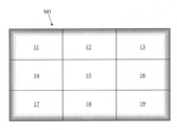
- FIG. 1 is a diagram showing an overall configuration of an example of a multi-display apparatus according to the present invention.
- the multi-display device M1 includes nine liquid crystal display devices 11 to 19 and an image distribution device 100.
- the multi-display device M1 includes nine liquid crystal display devices arranged in a horizontally long state, three vertically and three horizontally.
- the image distribution device 100 is connected to each of the nine liquid crystal display devices 11 to 19.
- the image distribution device 100 has nine image data for one screen image sent from an optical disk device such as a DVD device or a BD device, a personal computer, or the like so that it can be displayed on nine liquid crystal display devices 11 to 19.
- the image data corresponding to each screen is output to the liquid crystal display devices 11-19.
- the image distribution apparatus 100 can transmit image data for one screen to each of the liquid crystal display apparatuses 11 to 19 without dividing the image data as necessary. Further, the image distribution device 100 can transmit nine different images to the liquid crystal display devices 11 to 19, respectively.
- the image distribution apparatus 100 is well known in the art and will not be described in detail. In FIG. 1, solid arrows extending from the image distribution device 100 to the liquid crystal display devices 11 to 19 indicate the flow of image data.
- the liquid crystal display devices 11 to 19 are lined up in three vertical and horizontal directions so that the image display surfaces are arranged on the same surface to form one screen.
- the liquid crystal display devices 11 to 19 have the same size and configuration, and the screen formed by arranging the liquid crystal display devices 11 to 19 has the same aspect ratio as that of one liquid crystal display device (for example, the liquid crystal display device 11). And the size is 9 times (approximately 9 times).
- Each of the liquid crystal display devices 11 to 19 includes an image data acquisition unit 2. Details of the image data acquisition unit 2 will be described later.
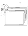
- FIG. 2 is an exploded perspective view of the liquid crystal display device
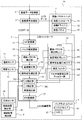
- FIG. 3 is a block diagram showing the configuration of the liquid crystal display device shown in FIG.
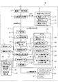
- the liquid crystal display device 1 includes an image data acquisition unit 2, an image signal processing unit 3, a liquid crystal panel unit 4, an LED controller 5 (light emission control means), and a backlight unit 6 (for image display).
- Light emitting means temperature sensor 71, luminance sensor 72, connection state detection unit 8 (state detection means), and the like.
- the liquid crystal display device 1 has a horizontally long rectangular shape as a whole and is integrally held by a frame-like bezel or the like.
- the image data acquisition unit 2 includes an external input interface that acquires image data sent from the image distribution apparatus 100.
- the image data acquisition unit 2 sends the acquired image data (image signal) to the image signal processing unit 3.
- the image data is data that specifies the brightness of each pixel for each frame, and thus specifies the content of a moving image (or still image).
- the image signal processing unit 3 receives image data from the image data acquisition unit 2, and based on this image data, LCD data which is data of light transmittance of each pixel, and light emission luminance of an LED 62 (described later) of the backlight unit 6. LED data representing is generated. Then, the LCD data is sent to the liquid crystal panel unit 4 and the LED data is sent to the LED controller 5, respectively.
- the liquid crystal panel unit 4 includes a liquid crystal controller 41, a liquid crystal driver 42, and a liquid crystal panel 43.
- the liquid crystal panel 43 has a rectangular shape in plan view, and is configured such that a pair of glass substrates are bonded together with a predetermined gap therebetween, and liquid crystal is sealed between the glass substrates.
- One glass substrate is provided with a switching element (for example, TFT (thin film transistor)) connected to a source wiring and a gate wiring orthogonal to each other, a pixel electrode connected to the switching element, an alignment film, and the like.
- the other glass substrate is provided with a color filter in which colored portions such as R (red), G (green, and B (blue)) are arranged in a predetermined arrangement, a common electrode, an alignment film, and the like.
- a polarizing plate is disposed on the outside of both substrates.
- the liquid crystal panel unit 4 is formed with color pixels of 1920 ⁇ 1080 dots, for example, for high vision.
- the liquid crystal panel unit 4 will be further described.
- the liquid crystal controller 41 generates a signal for driving the liquid crystal driver 42 based on the LCD data sent from the image signal processing unit 3 and sends the signal to the liquid crystal driver 42.
- the liquid crystal driver 42 switches the state of the switching element of each pixel of the liquid crystal panel 43 based on the signal received from the liquid crystal controller 41.
- the voltage of each pixel electrode provided in the liquid crystal panel 43 is adjusted according to the image data, the liquid crystal arranged in each pixel is driven, and the light transmission degree in each pixel is adjusted.
- the planar light from the backlight unit 6 is incident from the back surface of the liquid crystal panel unit 4, thereby displaying an image in the image display area of the liquid crystal panel 43.
- the backlight unit 6 is an illumination device that is driven by the LED control signal generated by the LED controller 5 and irradiates the liquid crystal panel unit 4 with planar light.
- the backlight unit 6 includes an LED mounting board (LED panel) 60, an LED driver 61, an LED (Light Emitting Diode) 62, an optical member 63 such as a diffusion plate or an optical sheet, and the like.
- the LED panel 60 has the LED 62 mounted on the mounting surface facing the liquid crystal panel unit 4.
- the LED panel 60 has a configuration in which a plurality of areas 600 are arranged vertically and horizontally.
- the area 600 is set so as to include at least one LED 62.
- the LED panel 60 is provided with an area 600 of 16 horizontal ⁇ 9 vertical (144 in total).
- the LED driver 61 drives the LED 62 for each area 600 based on an LED control signal described later from the LED controller 5 (light emission driving).
- the LED data and the PWM value generated based on the LED data (light emission luminance data, details will be described later) are given for each area 600.
- the LED 62 forms, for example, an LED unit in which LED chips that emit light of wavelengths of red, green, and blue (R, G, B) are gathered.
- the LED unit becomes white light as a whole by emitting light of each wavelength.
- another aspect may be sufficient.
- a white LED such as a pseudo white LED or a high color rendering white LED may be used in place of the LED unit described above, or an LED that emits light of a yellow (Y) wavelength in addition to the above RGB.
- a concentrated LED unit may be used.
- the brightness of the LED 62 is determined by the supplied current (supply current), and the light emission brightness of the LED 62 is substantially proportional to the supply current. Therefore, the LED data indicating the brightness of the LED 62 is the current supplied to each LED 62. It can be said that the data represents a value.
- the supply current to the LED 62 is controlled by PWM (pulse width modulation) control, and the LED controller 5 generates a duty ratio (hereinafter referred to as PWM value) used for PWM control based on the LED data.
- PWM value pulse width modulation
- the LED data is in the form of a 12-bit digital signal, and in the following description, the PWM value is also represented by 12 bits (0 to 4095).
- the backlight unit 6 can adjust the luminance of the LED 62 mounted on the LED panel 60 for each area 600.
- the backlight unit 6 can irradiate the area corresponding to the area 600 of the liquid crystal panel unit 4 with planar light (brightness distribution) adjusted in luminance for each area 600. This is an active backlight unit.
- the LED controller 5 generates an LED control signal for driving and controlling the backlight unit 6 based on the LED data.
- the LED data may include luminance information (APL value) of an image included in the image data.
- APL value luminance information
- the LED controller 5 can generate an LED control signal reflecting the luminance information of the image data.
- the LED control signal includes a PWM signal representing a PWM value for controlling the light emission of the LED 62.
- the LED controller 5 includes a serial / parallel conversion unit (S / P conversion unit) 51, a pulse width modulation unit 52, an individual variation correction unit 53, a temperature correction unit 54, a temporal deterioration correction unit 55, and a luminance correction unit 56 (luminance correction means). , A parallel serial conversion unit (P / S conversion unit) 57 and a memory 50.
- the S / P converter 51 converts the LED data sent as serial data from the image signal processor 3 into parallel data.
- the pulse width modulation unit 52 generates a PWM value based on the LED data.
- the individual variation correction unit 53 confirms the individual performance of the LED 62 in advance, and corrects the PWM value to eliminate the individual error. More specifically, when each LED chip constituting the LED 62 is lit at a predetermined PWM value, the PWM value is set so that the LED 62 has white light having a desired color. Thereafter, the plurality of LEDs 62 are turned on, and the PWM value is corrected for each area 600 so as to eliminate luminance unevenness as planar light. By performing the correction in this way, a PWM value in which the individual difference of the LEDs 62 (individual variation in luminance, luminance unevenness of planar light) is corrected is generated.
- correction processing using a general lookup table is employed. That is, the individual variation correction unit 53 performs correction processing with reference to the individual variation correction LUT 501 stored in the memory 50.
- the memory 50 includes various lookup tables (individual variation correction LUT 501, temperature) used in the correction units (individual variation correction unit 53, temperature correction unit 54, aging deterioration correction unit 55, luminance correction unit 56) included in the LED controller 5.
- a correction LUT 502, a temporal deterioration correction LUT 503, and a luminance correction LUT 504) are stored. Each LUT is referred to as necessary.
- the temperature correction unit 54 corrects a decrease in luminance of the LED 62 due to a temperature increase caused by the light emission of the LED 62.
- the temperature correction unit 53 receives the result of measuring the temperature of the LED 62 from the temperature sensor 71 as temperature data.
- the temperature correction unit 53 refers to the temperature correction LUT 502 based on the temperature data and corrects the PWM value for the LED 62 in each area 600. Thereby, the brightness
- the temperature data may be acquired at a predetermined frequency (for example, once per second).
- the aging deterioration correction unit 55 corrects the luminance reduction of the LED 62 due to the aging deterioration of the LED 62.
- the time degradation correction unit 62 acquires the brightness data of the LED 62 by the brightness sensor 72 when the accumulated lighting time reaches a predetermined time (for example, every 5000 hours).
- the temporal deterioration correction unit 55 refers to the temporal deterioration correction LUT 503 in the memory 50 based on the luminance data, and corrects the luminance, that is, corrects the PWM value for each LED 62.
- the planar light from the backlight unit 6 has uniform luminance that does not include luminance unevenness. It has the visual characteristic of recognizing that it is planar light.
- the luminance correction unit 56 reduces the luminance of the peripheral portion of the planar light from the backlight unit 6 to such a level that human eyes cannot recognize the luminance of the central portion.
- the PWM value is corrected. In this way, by reducing the luminance of the peripheral edge of the planar light, it is possible to reduce the power consumption of the LED 62 without degrading the display quality of the image (without feeling luminance unevenness).
- the brightness correction LUT 504 provided in the memory 50 is referred to, and the PWM value for driving the LED 62 for each area 600 is corrected.
- the luminance correction LUT 504 including the correction information corresponding to the area 600 arranged in the horizontal 16 ⁇ vertical 9 (144) is referred to.
- the luminance correction unit 56 performs correction based on information from the connection state detection unit 8 separately provided when the liquid crystal display device 1 is used as a part of the multi-display device M1.
- the connection state detection unit 8 includes a direction sensor 81 (direction detection means) that detects the installation direction (for example, landscape or portrait) of the liquid crystal display device 1 and the position where the liquid crystal display device 11 is formed in the multi-display device M1.
- a connection position detection unit 82 (connection position detection means) for detecting whether or not there is a problem.
- the connection state detection unit 8 sends connection information including information on the connection position and direction of the liquid crystal display device 1 in the multi-display device M1 to the luminance correction unit 56.
- the connection information may include more information such as the number of liquid crystal display devices constituting the multi-display device M1 in addition to the position and direction information.
- the memory 50 includes a multi-luminance correction filter group 505 corresponding to all positions of the multi-display apparatus M1 (for example, any position of 3 ⁇ 3 in the case of the multi-display apparatus M1 shown in FIG. 1). Is stored.
- the luminance correction unit 56 selects a table (correction data table) corresponding to the connection position from the multi-luminance correction filter group 505 based on the connection information from the direction sensor 81 and the connection position detection unit 82, and refers to the table. Then, the PWM value is corrected. The correction of the PWM value will be described in detail later.
- the P / S converter 57 outputs the LED data (including the PWM value) that has been subjected to the correction process transmitted as parallel data, as the serial data LED control signal (including the PWM control signal).
- the LED control signal is a signal including a PWM value given to each area 600 and a reference current value.
- the LED control signal is input to the LED driver 61 of the backlight unit 6, and the LED driver 61 performs light emission control (PWM control) of the LED 62 based on the LED control signal.
- the liquid crystal display device 1 has the above-described configuration.
- the image signal processing unit 3 generates LCD data and LED data based on the image data acquired from the image data acquisition unit 2, and transmits light through the liquid crystal panel unit 4.
- the degree and light emission of the backlight unit 6 are controlled, and an image is displayed.
- FIG. 4A is a schematic diagram showing a luminance distribution of planar light from the backlight unit when the liquid crystal display device is used alone
- FIG. 4B is a luminance when the planar light of FIG. 4A is used in a multi-display device. It is a figure which shows distribution.
- the luminance difference is made stronger than that of the originally used backlight unit.
- the luminance distribution is displayed in association with the backlight unit 6.
- the PWM value undergoes a plurality of correction processes, but the correction by the individual variation correction unit 53, the temperature correction unit 54, and the aging deterioration correction unit 55 eliminates variations in luminance of the planar light. It is correction for. These corrections have little to do with luminance unevenness in the planar light of the multi-display device M1.
- the correction by the luminance correction unit 56 is a correction that reduces the luminance of the peripheral portion of the planar light, and causes uneven luminance in the planar light of the multi-display device M1. Therefore, in the following description, correction by the luminance correction unit 56 will be described.
- the backlight unit 6 irradiates planar light with a bright central portion (high luminance) and a dark peripheral portion (low luminance) in consideration of visual characteristics.
- the luminance distribution as shown in FIG. 4A is given to the planar light by adjusting the luminance of the LED 62.
- the backlight unit 6 adjusts the brightness of the LED 62 for each area 600.
- the luminance of the LED 62 (luminance for each area 600) is represented by a PWM value.
- the PWM value is expressed by 12 bits (0 to 4095)
- the PWM value is displayed as 0 when the brightness of the LED 62 is zero.
- the PWM value is displayed as 4095.
- the luminance correction unit 56 assumes that the PWM value of the planar light before correction is 4095 in all areas 600 (LEDs 62 included). Actually, it may vary depending on the input image data and the various correction processes described above.
- the luminance correction unit 56 corrects the PWM value with reference to the luminance correction LUT 504 stored in the memory 50.
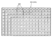
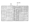
- FIG. 5A is a diagram illustrating an example of a luminance correction LUT for performing luminance correction
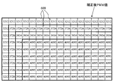
- FIG. 5B is a diagram illustrating PWM values in a partial area corrected by the luminance correction LUT in FIG. 5A.
- the luminance correction LUT 504 shown in FIG. 5A is an 8-bit correction coefficient lookup table.
- the luminance correction LUT 504 is 16 ⁇ 9 matrix data corresponding to the area 600 of the backlight unit 6.
- the luminance correction LUT 504 has a central portion (10 ⁇ 3 portion) value of 255, an outer side of 245, an outer side of 232, and an outermost side of 200.
- the region is surrounded by a thick line for easy understanding.
- the luminance correction LUT 504 is a correction coefficient for correcting the PWM value corresponding to each area 600.
- the correction result is as shown in FIG. 5B.
- the PWM value is corrected as follows.
- PWM value 4095 ⁇ 200 / 255 ⁇ 3212
- the PWM value is corrected as follows.
- PWM value 4095 ⁇ 232 / 255 ⁇ 3726
- the correction coefficient is 245, and the PWM value is corrected as follows.
- PWM value 4095 ⁇ 245 / 255 ⁇ 3934
- the 13 ⁇ 3 portion in the center uses a correction coefficient of 255, that is, a PWM value without correction processing as the PWM value.
- PWM value 4095
- the luminance correction unit 56 performs the PWM value correction process according to the above-described procedure, and generates an LED control signal generated based on the PWM value having a luminance distribution.
- the LED driver 61 adjusts the luminance of the LED 62 for each area 600 by performing light emission control of the LED 62 with this LED control signal.
- the luminance correction LUT 504 As shown in FIG. 5A, that is, by correcting the PWM value of each area 600 as shown in FIG. 5B, the luminance distribution as shown in FIG. 4A is obtained. Planar light is emitted from the backlight unit 6.
- the liquid crystal display device 11 When the liquid crystal display device 11 is used alone, since the image is displayed with the planar light having the luminance distribution shown in FIG. 4A, the luminance of the central portion of the image display area is high and the luminance of the peripheral portion is low. Therefore, it is difficult for the observer to perceive uneven brightness, and the power consumption of the backlight unit 6 can be reduced.
- the liquid crystal display device 1 is used as a part of the multi-display device M1
- the same nine liquid crystal display devices 11 to 19 as the liquid crystal display device 1 are arranged vertically and horizontally, and the luminance of the planar light from the backlight unit 6 of each liquid crystal display device 11 to 19 is arranged.
- the luminance distribution of the planar light used for the display of the multi-display device M1 becomes a luminance distribution as shown in FIG. 4B.
- the upper side and the left side constitute the peripheral portion of the multi-display device M1, but the lower side and the right side are not part of the peripheral portion of the multi-display device M1.
- some or all of the sides do not coincide with the peripheral edge of the multi-display device M1.
- a low luminance region is formed in a portion other than the edge portion of the planar light as shown in FIG. 4B.
- This low-luminance part is formed near the central part and can be recognized by human eyes. That is, when the PWM value is corrected by the luminance correction LUT 504 as shown in FIG. 5A, an image with uneven luminance is displayed on the multi-display device M1.
- the backlight unit 6 of each of the liquid crystal display devices 11 to 19 has a luminance distribution (periphery when the multi-display device M1 is regarded as one display device) in consideration of the visual field characteristics of human eyes. It is preferable that the planar light is emitted from the backlight of each liquid crystal display device so that the luminance distribution of the part is low).
- An example of the luminance distribution of the planar light in the multi display device M1 is shown in FIG.
- the planar light shown in FIG. 6 is given a luminance distribution such that the multi-display device M1 is regarded as a single display device, the luminance of the central portion of the display device is high, and the luminance of the peripheral portion is low.
- planar light having such a luminance distribution it is necessary to emit planar light having a different luminance distribution from the backlight unit 6 provided in each of the liquid crystal display devices 11 to 19.
- a multi-display when used as a liquid crystal display device constituting the multi-display device M1 is provided in addition to the luminance correction LUT 504 (shown in FIG. 5A) when the liquid crystal display devices 11 to 19 are used as a single unit.
- a luminance correction filter group 505 is provided in addition to the luminance correction filter group 505 .
- the multi-luminance correction filter group 505 includes nine tables corresponding to the respective positions of the liquid crystal display devices 11 to 19. Each table has 144 (16 horizontal x 9 vertical) correction coefficients, which is the same as the number of areas 600 of the backlight unit 6.
- FIG. 7A is a diagram showing a part of the multi-luminance correction filter group
- FIG. 7B is a diagram showing PWM values corrected by the multi-luminance correction filter group shown in FIG. 7A.
- a table 5051 shown in FIG. 7A is a table for correcting the PWM value of the liquid crystal display device 11 in the multi-display device M1 shown in FIG. Note that the multi-luminance correction filter group 505 performs correction with 8 bits in the same manner as the luminance correction LUT 504.
- the correction coefficient of the area 600 adjacent to the upper side and the left side is 200
- the inner side is 232
- the inner side is 245, and the remaining is 255.
- the table 5051 is 255 in the 13 ⁇ 9 portion in the lower right portion.
- the PWM value of area 600 that is correction coefficient 200 is 3212
- the PWM value of area 600 that is correction coefficient 232 is 3726
- the PWM value of area 600 that is correction coefficient 245 is 3934
- the PWM value of area 600 that is correction coefficient 255 is PWM.
- the value is 4095.
- the backlight unit 6 of the liquid crystal display device 11 can irradiate planar light with low luminance at the peripheral portion of the upper left corner. Yes (see FIG. 6).
- FIG. 8A is a diagram showing a table of a part different from FIG. 7A
- FIG. 8B is a diagram showing PWM values corrected by the table of FIG. 8A
- FIG. 8A is a table for correcting the PWM value of the liquid crystal display device 12 at the upper center of the multi-display device M1.
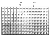
- the table 5052 for correcting the PWM value of the backlight unit 6 provided in the liquid crystal display device 12 is as follows.
- the correction coefficient of the area 600 along the upper side is 200
- the correction coefficient of the area 600 below it is 232
- the correction coefficient of the area 600 below it is 245
- the remaining correction coefficients are 255.
- the PWM values corrected by this table 5052 are as shown in FIG. 8B.
- the backlight unit 6 of the liquid crystal display device 12 can emit planar light having a luminance distribution as shown in FIG.
- FIG. 9 is a schematic diagram showing an example of a multi-luminance correction filter group.
- FIG. 9 is a diagram showing the concept of the configuration of the multi-luminance correction filter group.
- the multi-luminance correction filter group 505 includes tables 5051 to 5059 corresponding to the positions of the liquid crystal display devices 11 to 19, respectively.
- the brightness correction unit 56 needs to refer to a table corresponding to the position of the liquid crystal display device from among these tables 5051 to 5059. Therefore, the luminance correction unit 56 includes the direction information of the installation direction (horizontal or vertical) of the liquid crystal display device detected by the direction sensor 81 and the liquid crystal display device 1 detected by the connection position detection unit 82 of the multi-display device M1. Connection information including connection position information indicating which position it is, that is, which liquid crystal display device among the liquid crystal display devices 11 to 19 is sent from the connection state detection unit 8.
- connection position detection unit 82 may detect the connection position by a liquid crystal display device arranged next to the liquid crystal display device when the liquid crystal display device is connected so as to form a multi-display device. For example, when it is detected that the liquid crystal display device is connected to the lower side and the right side, the liquid crystal display device 1 is detected to be disposed at the upper left of the multi-display device M1, that is, the liquid crystal display device 11. The detection of the connection position is not limited to this.
- the luminance correction unit 56 When the luminance correction unit 56 obtains the direction information and the connection position information, the luminance correction unit 56 refers to the corresponding tables 5051 to 5059 in the multi luminance correction filter group 505 stored in the memory 50. For example, when the brightness correction unit 56 obtains information about the liquid crystal display device 11, the brightness correction unit 56 refers to the table 5051 and corrects the PWM value.
- the multi-display device M1 there may be variations in the color and brightness of the planar light for each liquid crystal display device. Therefore, after correcting the PWM value, information on the luminance level may be exchanged between adjacent liquid crystal display devices so that the luminance level is matched. By correcting in this way, it is possible to correct the luminance variation between the liquid crystal display devices, and it is possible to improve the image display quality in the multi-display device.
- the multi-display device M1 that can reduce the power consumed by the backlight unit without the observer recognizing luminance unevenness.
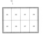
- FIG. 10 is a diagram showing the luminance distribution of another example of the multi-display device.
- the liquid crystal display devices 1 are arranged in a horizontally long form.
- the multi-brightness correction filter group 505 stored in the memory 50 of the liquid crystal display device 1 is similar to the tables corresponding to the liquid crystal display devices 11 to 19 of the multi-display device M1, and each liquid crystal constituting the multi-display device M2. Tables (not shown) corresponding to the display devices 101 to 108 are also provided.
- connection state detection unit 8 of the liquid crystal display device 1 detects that the direction sensor 81 is installed in the vertical direction, and the connection position detection unit 82 detects the connection position.
- the connection state detection unit 8 sends information on the installed direction (direction information) and information on the connection position (connection position information) to the luminance correction unit 56.
- the luminance correction unit 56 appropriately selects and references a table corresponding to one of the liquid crystal display devices 101 to 108 from the multi-luminance correction filter group 505 based on the direction information and the connection position information, and performs PWM Correct the value.
- the brightness correction unit 56 detects the connection state (3 ⁇ 3 or 4 ⁇ 2) of the multi-display device based on the direction information detected by the direction sensor 81, and performs brightness correction according to the connection state. Is possible.
- the luminance and / or luminance distribution of the planar light may be adjusted depending on the installation location, display image, power consumption, and the like. For example, a mode that displays a bright screen used when installing in a bright place, a mode that displays a screen with an intermediate brightness that balances the brightness and power consumption of the image, and a dark screen that reduces power consumption. There are three display modes (referred to as display modes).
- the luminance correction LUT 505 includes a table for each mode.
- the luminance correction unit 56 converts the table corresponding to one of the liquid crystal display devices 11 to 19 based on the direction information, the connection position information, and the mode information from the connection state detection unit 8 into the multi-luminance correction filter group 505. Select from.
- the display mode information may be included in the LED data transmitted from the image signal processing unit 3, or may be separately transmitted from the image signal processing unit 3 to the luminance correction unit 56.
- the multi-brightness correction filter group 505 includes tables corresponding to the liquid crystal display devices 11 to 19 or the liquid crystal display devices 101 to 109, respectively. Therefore, the data of the luminance correction LUT 505 is the number of areas of the liquid crystal display device ⁇ the number of bits of the correction coefficient ⁇ (the number of liquid crystal display devices of the multi display device M1 + the number of liquid crystal display devices of the multi display device M2) ⁇ (display mode). Number) (here, 31104 bits).
- the multi-luminance correction filter group 505 a portion corresponding to the connection position may be referred to from the tables (48 ⁇ 27 and 36 ⁇ 32) corresponding to the entire multi-display device. Also in this case, the data amount is the same as the case where a table corresponding to each liquid crystal display device is provided.
- the memory 50 of the LED controller 5 of each of the liquid crystal display devices 11 to 19 stores a multi-luminance correction filter group 505.
- the above-described multi-display device uses a liquid crystal display device that can emit planar light having a uniform luminance distribution when the PWM value is not corrected.
- luminance luminance
- an image display device having a non-uniform distribution There is an image display device having a non-uniform distribution.
- the multi-luminance correction filter group includes a table corresponding to the liquid crystal display device using a backlight unit with non-uniform luminance distribution. With the configuration, the luminance distribution of the multi-display device can be optimized.
- a multi-display device including both a liquid crystal display device with a non-uniform luminance distribution and a liquid crystal display device with a uniform luminance distribution
- the multi-luminance correction filter group and the luminance corresponding to the liquid crystal display device with a non-uniform luminance distribution Both of the multi-luminance correction filter groups corresponding to the liquid crystal display device having a uniform distribution must be provided, and the storage capacity is increased. Therefore, in a liquid crystal display device with a non-uniform luminance distribution, the multi-display device is corrected so as to obtain a uniform luminance distribution, and then corrected so as to obtain an optimal luminance distribution when viewed as a multi-display device. Can be optimized.
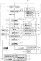
- FIG. 11 is a block diagram showing the configuration of the liquid crystal display device.
- a liquid crystal display device 1 ⁇ / b> A illustrated in FIG. 11 includes a luminance correction unit 56 that includes a uniformization unit 561 and a correction unit 562.
- the liquid crystal display device 1A first corrects the PWM value corresponding to each area 600 so that the uniformizing unit 561 can emit planar light having a uniform luminance distribution from the backlight unit 6 of the liquid crystal display device 1A.
- a correction table stored in the memory 50 is used for correction. This correction table is a configuration opposite to that of the luminance correction table, that is, a table having an inclination such that the correction coefficient at the center is small and increases toward the outside.
- the correction unit 562 has the same configuration as that of the luminance correction unit 56 described above. That is, based on the connection information of the liquid crystal display device, a table corresponding to the liquid crystal display device is selected from the multi-luminance correction filter group 505, and the PWM value is corrected. In this way, the luminance level between the adjacent liquid crystal display devices can be made uniform by making it uniform once. As a result, even if a multi-display device is configured using a liquid crystal display device having a nonuniform luminance distribution, an image of the luminance distribution taking into consideration the visual characteristics of the human eye can be displayed, and luminance unevenness can be displayed to the observer. Luminance correction can be performed without being recognized.
- FIG. 12 is a block diagram illustrating another example of the liquid crystal display device
- FIG. 13 is an explanatory diagram of correction of the PWM value by the luminance correction unit.
- the liquid crystal display device 1 ⁇ / b> B has the same configuration as the liquid crystal display device 1 shown in FIG. 3 except for the luminance correction unit 58. Description of is omitted.
- the luminance correction unit 58 includes an X correction unit 581 and a Y correction unit 582. Note that the luminance correction shown in FIG. 13 is an example, and the PWM value set for each area 600 is 4095.
- the X correction unit 581 corrects the PWM value for each row (X correction) for each row with the rows (St1 to St9) arranged in the horizontal direction (X direction) as a group.
- the Y correction unit 582 corrects the PWM value for each column (Y correction) for each column with the columns (Pr1 to Pr16) arranged in the vertical direction (Y direction) as a group.
- the memory 50 has a filter (X filter) 5061 having a correction coefficient for correcting the rows (St1 to St9) and a filter (Y filter) having a correction coefficient for correcting the column. ) 5062 is stored.
- the luminance correction unit 58 performs X correction and then Y correction on the PWM value before correction.
- the luminance correction unit 58 refers to the X filter 5061 when performing X correction.
- the X filter 5061 has 16 correction coefficients arranged in the X direction. With reference to the X filter 5061, correction is performed in units of rows from the first row St1 to the ninth row St9 in order of the PWM value for each area 600, and the first row St1 to the ninth row St9 are arranged as before.
- the corrected numerical values are as shown in FIG. 13, and the calculation formula for correction is the same as that of the luminance correction unit 56, and therefore will be omitted.
- the Y filter 5062 for performing Y correction has nine correction coefficients arranged in the Y direction.
- the luminance correction unit 58 refers to the Y filter 5062, and corrects the PWM value for each area 600 in units of columns from the left of the PWM value to the 16th column Pr16 in order from the first column Pr1.
- the first row Pr1 to the 16th row Pr16 are arranged (see FIG. 13). Even with such a correction method, it is possible to emit planar light having a high luminance in the central portion and a low luminance in the peripheral portion.
- the memory 50 also includes a multi-brightness correction filter group 507 for correcting the brightness of the multi-display device.
- a configuration M1 including nine (3 ⁇ 3) liquid crystal display devices will be described as an example of the multi-display device.
- the multi-luminance correction filter group 507 includes an X filter 5071 for each connection position of the liquid crystal display device so that the liquid crystal display device 1B can be used as a liquid crystal display device at any position constituting the multi-display device.
- Y filter 5072 correction data table).
- the brightness correction unit 58 corresponds to the position of the station layer display device in the multi-display device from the multi-luminance correction filter group 507.
- the PWM value is corrected based on the X filter 5071 and the Y filter 5072. Since the X correction and the Y correction are as described above, details are omitted.
- the correction filter 506 and the multi-luminance correction filter group 507 are used, it is necessary to correct the PWM value for each row or column.
- the information amount of the multi-luminance correction filter group 507 is significantly smaller than that of the multi-luminance correction filter group 505 using a table in which correction coefficients are set for each area 600.
- the information amount of the X filter 5071 is the number of areas 600 in one row ⁇ the number of bits of the correction coefficient ⁇ (the number of liquid crystal display devices of the multi display device M1 + the number of liquid crystal display devices of the multi display device M2) ⁇ (the number of modes) ( Here, 6528 bits).
- the information amount of the Y filter 5072 is the number of areas 600 in one column ⁇ the number of bits of the correction coefficient ⁇ (the number of liquid crystal display devices of the multi display device M1 + the number of liquid crystal display devices of the multi display device M2) (3672 bits).
- the information amount of the multi-luminance correction filter group 507 is 10200 bits.
- the information amount of the multi-luminance correction filter group 507 is 10200 bits, and the information amount can be significantly reduced as compared to the information amount of 31104 bits of the information amount of the multi-correction LUT 505. It is possible to reduce the capacity of the memory 50 by using such a multi-brightness correction filter group 507 and including the brightness correction unit 58 that performs correction using the multi-brightness correction filter group 507.
- FIG. 14 is a diagram showing an overall configuration of another example of the multi-display device according to the present invention
- FIG. 15 is a block diagram showing a configuration of a liquid crystal display device constituting the multi-display device shown in FIG.
- the basic configuration of the liquid crystal display device is substantially the same as that of the liquid crystal display device shown in FIG.
- the multi-display device M3 shown in FIG. 14 includes an external controller 200 (external control means) that is connected to the liquid crystal display devices 11 to 19 of the multi-display device M3 and provides connection position information and direction information.
- the external controller 200 is disposed inside the image distribution device 100, but is not limited to this, and is provided separately from the image distribution device 100. Also good.
- the external controller 200 provides connection position information and direction information to the connected liquid crystal display devices 11 to 19.
- the external controller 200 is directly connected to the LED controllers 5 of the liquid crystal display devices 11 to 19, but the present invention is not limited to this, and the main controller (not shown) of the liquid crystal display device is used. After inputting, the structure which transmits to the luminance correction part 56 of the LED controller 5 from a main controller may be sufficient. Further, the external controller 200 may provide connection position information to each liquid crystal display device, and the direction information may be detected by the direction sensor 81 of each liquid crystal display device.
- liquid crystal display device 1C constituting the multi-display device M3
- the configuration of the liquid crystal display device 1C will be described as a representative.
- the liquid crystal display device 1C shown in FIG. 15 has the same configuration as the liquid crystal display device 1 shown in FIG. 3 except that the connection state detection unit 8 is omitted, and substantially the same parts are denoted by the same reference numerals, The description of the same part is omitted.
- the luminance correction unit 56 of the liquid crystal display device 1 ⁇ / b> C is connected to the external controller 200, and receives direction information and connection position information from the external controller 200. Based on the direction information and connection position information, the luminance correction unit 56 selects and refers to an appropriate table among the tables 5051 to 5059 corresponding to the liquid crystal display devices 11 to 19 from the multi-luminance correction filter group 505. The PWM value is corrected.
- the external controller 200 detects the direction information and the connection position information, and functions as the connection state detection unit 8 that transmits the connection information including each information. Therefore, the connection state detection of each liquid crystal display device is performed.
- the unit 8 (when the direction information is detected by the direction sensor 81) can be omitted, and the configuration of the liquid crystal display device can be simplified.
- the external controller 200 determines an appropriate table among the tables included in the multi-luminance correction filter group 505, and transmits information for specifying the table and table specification information from the external controller 200 to the luminance correction unit 56. It may be. According to this configuration, the luminance correction unit 56 does not need to perform an operation (calculation) for selecting an appropriate table from the multi-luminance correction filter group 505, and the load on the luminance correction unit 56 can be reduced accordingly.
- the external controller 200 may be mounted on any of the liquid crystal display devices that constitute the multi-display device M3.
- the liquid crystal display device 1 (1B, 1C) includes the multi-luminance correction filter group 505 or the multi-luminance correction filter group 507.
- the arrangement of the multi-display device for example, horizontal 3 ⁇ vertical 3 or horizontal 4 ⁇ vertical 2 needs to be determined in advance.
- FIG. 16 is a diagram showing a state in which a plurality of liquid crystal display devices are arranged.
- FIG. 16 shows an example in which the liquid crystal display device is used horizontally.
- the size of the image display unit can be changed by changing the number of liquid crystal display devices arranged and the arrangement direction.
- the portion that has been the peripheral portion is no longer the peripheral portion.
- seven liquid crystal display devices are added to a multi-display device (configuration of the multi-display device M1 shown in FIG. 1 and the like) in which the liquid crystal display devices are arranged in 3 ⁇ 3.
- the multi-display device M4 is arranged vertically 4, the lower sides of the liquid crystal display devices 17 to 19 constituting the lower edge portion of the multi-display device M1 are not edge portions.
- the right sides of the liquid crystal display devices 13, 16, and 19 constituting the right side edge are no longer edge parts.
- the luminance is applied to the lower and right edge portions of the multi-display device M1.
- a low-luminance portion occurs in the vicinity of the central portion, so that it does not match the visual characteristics of the human eye and uneven luminance is easily observed.
- FIG. 17 is a block diagram showing a configuration of a liquid crystal display device used in the multi-display device according to the present invention.
- an external controller 300 is also shown.
- the external controller 300 includes a memory 301, and a multi-luminance correction filter group 302 is stored in the memory 301.
- the multi-brightness correction filter group 302 includes a table for correcting the PWM value in each liquid crystal display device when the horizontally long liquid crystal display devices are arranged in 2 ⁇ 2 to 5 ⁇ 5, and four vertically long liquid crystal display devices. And a table for correcting the PWM value in each liquid crystal display device when arranged in ⁇ 2, 2 ⁇ 5, 3 ⁇ 4, and 3 ⁇ 5.
- the external controller 300 is connected to each liquid crystal display device constituting the multi-display device M4, and has a function of detecting direction information and connection position information of each liquid crystal display device.
- the external controller 300 recognizes the shape of the multi-display device M4 (the number of liquid crystal display devices) from the direction information and the connection position information, and selects a table corresponding to each liquid crystal display device from the multi-luminance correction filter group 302. Then, the table information is transmitted to each liquid crystal display device.
- the liquid crystal display device 1D When receiving the table from the external controller 300, the liquid crystal display device 1D corrects the PWM value based on the table. As described above, when the table information is supplied from the external controller 300 to the liquid crystal display device 1D, the table information is within a predetermined range. However, even if the number of the liquid crystal display devices constituting the multi-display device is changed, The luminance of the planar light from the light unit 6 can be corrected. In addition, since the multi-luminance correction filter group need not be stored in the liquid crystal display device 1D, the capacity of the memory 50 can be reduced.
- the multi-luminance correction filter group 302 having a table in which correction coefficients for each area 600 similar to the multi-luminance correction filter group 505 are arranged in a matrix is described as an example.
- the same configuration as the multi-luminance correction filter group 507 may be used. Using the configuration of the multi-luminance correction filter group 507 reduces the amount of information sent from the external controller 300 to each liquid crystal display device 1D and facilitates control.
- FIG. 18 is a diagram showing an overall configuration of still another example of the multi-display apparatus according to the present invention.
- the multi-display device M5 is usually used as one image display device.
- the brightness gradient information 403 when the multi-display device M5 is viewed as one image display device is stored in the memory 401.
- the luminance gradient information in the horizontal direction and the luminance gradient information in the vertical direction are ratios (or weights) to the luminance (maximum luminance) at the maximum output of the LED 62, respectively.
- the luminance gradient information 403 is information including the horizontal and vertical relative coordinates of the image display unit and the luminance ratio (weight) at that position. That is, the luminance gradient information 403 is data representing the luminance distribution with the relative coordinates and relative luminance of the image display unit.
- the calculation unit 402 of the external controller 400 generates a multi-luminance correction filter group based on the arrangement of the liquid crystal display devices in the multi-display device M5 and the luminance gradient information 403.
- the luminance gradient information 403 is a luminance ratio based on the relative coordinates of the image display unit, so that a multi-luminance correction filter group can be generated even if the size of the multi-display device M5 changes. Thereby, even if the arrangement of the liquid crystal display device is changed, the multi-display device M5 can perform appropriate luminance correction.
- the arithmetic unit 402 generates a multi-luminance correction filter group corresponding to the multi-luminance correction filter group 507, and transmits an appropriate one of the multi-luminance correction filter group to each liquid crystal display device. You may do it.
- the calculation unit 402 is provided in the LED controller 5 of each liquid crystal display device, receives luminance gradient information 403 corresponding to the position of each liquid crystal display device from the external controller 400, and stores a table and a filter inside the LED controller 5. You may make it produce
- FIG. 19 is a diagram showing the overall configuration of still another example of the multi-display device according to the present invention
- FIGS. 20A and 20B are diagrams showing the luminance distribution of planar light in the multi-display device shown in FIG.
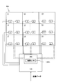
- the multi-display device M6 includes an external controller 500 including a human sensor 5001.
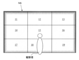
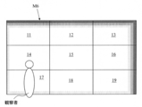
- the multi-display device M6 is often larger than an observer when it is configured by arranging large liquid crystal display devices. Depending on the observation position, the observer changes between a place that is easily visible (a place that is easily visible) and a place that is difficult to see (a place that is difficult to see).
- the multi-display device M6 when there is an observer in the center of the front of the multi-display device M6, the upper and left and right side edges are difficult to see, and the luminance of the part may be low.
- the height of the observer's eyes is shifted to the lower side of the multi-display device M6, so that the lower side is more likely to be dead than the above three sides. Therefore, in the multi-display device M6, a human sensor 5001 detects the position of the observer, and based on the detection result, the table is such that the luminance is high when it is easily visible and the luminance is low when it is difficult to visually recognize.
- the brightness correction unit 56 corrects the PWM value by referring to the table.
- the external controller 500 selects or generates a table so that the luminance on the left side of the multi-display device M6 is high and the luminance on the upper right side is low.
- a human sensor may be used instead of the external controller 500 provided in each liquid crystal display device. In this case, the results detected by the human sensor of each liquid crystal display device are collected in the external controller, and the external controller 500 comprehensively judges and recognizes the position of the observer, so that it can be accurately recognized. is there.
- the external controller 500 may generate or select a multi-luminance correction filter group instead of the multi-luminance correction filter group.
- Corresponding tables and filters may be generated by the LED controller 5 of each liquid crystal display device.
- FIG. 21 is a schematic view when an image is displayed in still another example of the multi-display device according to the present invention
- FIG. 22 is a block diagram showing a configuration of a liquid crystal display device constituting the multi-display device shown in FIG.
- FIG. 23 is a diagram showing an example of a table provided in the multi-luminance correction filter group provided in the liquid crystal display device shown in FIG.
- the multi-display device M7 can display a 16: 9 image, and the multi-display device M7 shown in FIG. 21 displays a conventional 4: 3 image. At this time, there is a method in which a 4: 3 image is displayed while being stretched in the horizontal direction, but the display quality is deteriorated, so that black band portions (Bw) are displayed on both the left and right sides as shown in FIG. There are many cases.
- the image signal processing unit 3 displays LED information together with information on the image (in this case, information indicating that a black belt portion exists). Data is sent to the LED controller 5. As shown in FIG. 22, in the liquid crystal display device 1 ⁇ / b> E, image information input to the LED controller 5 is sent to the luminance correction unit 59.
- the luminance correction unit 59 selects a multi-luminance correction filter group 509 for performing luminance correction from the memory 50 based on image information, and corrects the PWM value based on the multi-luminance correction filter group.
- the table 5091 included in the multi-luminance correction filter group 509 is as shown in FIG.
- the table shown in FIG. 23 is a table for correcting the PWM value of the upper left liquid crystal display device 11 of the multi-display device M7 shown in FIG.
- the black belt portion Bw can express black more black by turning off the LED 62. Thereby, display quality can be improved. Therefore, the table 5091 employs 0 as the correction coefficient for the black belt portion Bw. In the area Ma where the image is displayed, the correction coefficient is set so that the luminance of the edge portion is lowered.
- the multi-luminance correction filter group 509 includes a table that takes into account the black belt portion Bw corresponding to the other liquid crystal display devices 12 to 19.
- the memory 50 is also provided with a multi-luminance correction filter group 505 as shown in the first embodiment, for example, and the luminance correction unit 59 is an image including the black belt portion Bw.
- the multi-luminance correction filter group 509 is selected.
- the luminance of the image portion excluding the black belt portion Bw is corrected, the planar light of the luminance distribution considering the visual characteristics of the human eye can be used, and the luminance unevenness is recognized by the observer. Therefore, power consumption can be reduced.
- characters, images, etc. are displayed on the black belt part in data broadcasting, etc.
- a multi-luminance correction filter group having a table in which the correction coefficient of the black belt part is not zero is referred to. You may do it.
- the black band portion has low luminance
- the luminance correction unit 59 corrects the PMW value of the black band portion with a predetermined low correction coefficient (for example, 128 in an 8-bit table). You may make it do.
- the multi-luminance correction filter group may constitute a filter instead of a table.
- the multi-luminance correction filter group 509 is stored in the memory in advance.
- the present invention is not limited to this, and a table corresponding to the LED controller 5 or the external controller of each liquid crystal display device.
- the configuration may include a calculation unit that generates a filter.
- the pulse width modulation method for changing the PWM value is used to determine the current supplied to the LED 62, but the current value may be directly corrected.
- a current value setting unit for setting the current value supplied to the LED 62 is arranged instead of the pulse width modulation unit, and the current value is set by the individual variation correction unit, the temperature correction unit, the aging deterioration correction unit, and the luminance correction unit. You may make it correct
- the PWM value associated with the area 600 is corrected for the LED 62.
- the LED 62 may be a red (R) LED chip, a green (G) LED chip, or a blue (B ) LED chip may be provided, the PWM value for each chip may be corrected.
- a correction table for each chip may be provided.
- the liquid crystal display devices constituting the multi-display device and the connection between the liquid crystal display devices and the external control unit may be wired connections.
- a wireless connection may be used.
- wired connection it is difficult to be affected by surrounding radio wave conditions, and in the case of wireless connection, wiring can be omitted, so that a multi-display device can be easily constructed.
- the multi-display device is widely arranged at a place where many observers gather such as a station, an event venue, a stadium, etc., and transmits information to many observers at once (displays an image). Therefore, it can be used as an image display device.
Landscapes
- Engineering & Computer Science (AREA)
- Multimedia (AREA)
- Signal Processing (AREA)
- Theoretical Computer Science (AREA)
- General Physics & Mathematics (AREA)
- Physics & Mathematics (AREA)
- Social Psychology (AREA)
- General Engineering & Computer Science (AREA)
- Business, Economics & Management (AREA)
- General Health & Medical Sciences (AREA)
- Health & Medical Sciences (AREA)
- Computer Hardware Design (AREA)
- Life Sciences & Earth Sciences (AREA)
- Computer Networks & Wireless Communication (AREA)
- Biodiversity & Conservation Biology (AREA)
- Environmental Sciences (AREA)
- Marketing (AREA)
- Emergency Management (AREA)
- Environmental & Geological Engineering (AREA)
- Ecology (AREA)
- Databases & Information Systems (AREA)
- Human Computer Interaction (AREA)
- Remote Sensing (AREA)
- Software Systems (AREA)
- Control Of Indicators Other Than Cathode Ray Tubes (AREA)
- Liquid Crystal (AREA)
Abstract
L'invention a pour objectif de fournir un affichage avec une qualité d'image élevée tout en réduisant la consommation d'énergie d'un dispositif multi-affichages. Le dispositif multi-affichages de l'invention comprend : un moyen d'émission d'affichage d'image (6) qui amène des éléments luminescents (62) disposés dans chaque région d'une pluralité de régions (600) à émettre de la lumière pour former une lumière planaire ; et un moyen de contrôle d'émission de lumière (5) qui génère des données de luminosité d'émission de lumière pour chacune des régions (600) commandant les éléments luminescents (62) ; le moyen de contrôle de l'émission de lumière (5) comprenant un moyen de correction de luminosité (56) qui corrige les données de luminosité de l'émission de lumière d'après les informations de connexion qui sont des informations concernant les directions d'installation ou les positions de connexion des dispositifs d'affichage d'images (11 à 19).
Priority Applications (1)
| Application Number | Priority Date | Filing Date | Title |
|---|---|---|---|
| US14/113,629 US9240145B2 (en) | 2011-04-27 | 2012-04-20 | Multi-display device and image display device |
Applications Claiming Priority (2)
| Application Number | Priority Date | Filing Date | Title |
|---|---|---|---|
| JP2011-099896 | 2011-04-27 | ||
| JP2011099896 | 2011-04-27 |
Publications (1)
| Publication Number | Publication Date |
|---|---|
| WO2012147651A1 true WO2012147651A1 (fr) | 2012-11-01 |
Family
ID=47072171
Family Applications (1)
| Application Number | Title | Priority Date | Filing Date |
|---|---|---|---|
| PCT/JP2012/060721 Ceased WO2012147651A1 (fr) | 2011-04-27 | 2012-04-20 | Dispositif multi-affichages et dispositif d'affichage d'image |
Country Status (2)
| Country | Link |
|---|---|
| US (1) | US9240145B2 (fr) |
| WO (1) | WO2012147651A1 (fr) |
Cited By (3)
| Publication number | Priority date | Publication date | Assignee | Title |
|---|---|---|---|---|
| JP2013088629A (ja) * | 2011-10-18 | 2013-05-13 | Sharp Corp | マルチディスプレイシステム |
| CN106710571A (zh) * | 2017-03-23 | 2017-05-24 | 海信集团有限公司 | 显示控制方法、显示控制器及拼接显示系统 |
| WO2023123240A1 (fr) * | 2021-12-30 | 2023-07-06 | 京东方科技集团股份有限公司 | Écran en mosaïque et procédé de compensation d'affichage associé |
Families Citing this family (24)
| Publication number | Priority date | Publication date | Assignee | Title |
|---|---|---|---|---|
| JP2014194525A (ja) * | 2013-02-28 | 2014-10-09 | Canon Inc | 画像表示装置、画像出力装置、及びその制御方法 |
| US9373288B2 (en) | 2014-08-28 | 2016-06-21 | Microsoft Technology Licensing, Llc | Configurable, localized backlighting with planar emission devices |
| JP6378031B2 (ja) * | 2014-10-03 | 2018-08-22 | シャープ株式会社 | 配置判定装置、配置判定方法、プログラム、記録媒体 |
| CN104750451B (zh) * | 2015-04-10 | 2017-10-31 | 京东方科技集团股份有限公司 | 拼接器及拼接显示系统 |
| KR102418003B1 (ko) * | 2016-01-04 | 2022-07-07 | 삼성전자주식회사 | 복수의 디스플레이 장치들을 이용한 콘텐츠의 디스플레이 |
| KR20180051976A (ko) * | 2016-11-09 | 2018-05-17 | 엘지전자 주식회사 | 디스플레이 장치 |
| US10916191B2 (en) | 2017-02-13 | 2021-02-09 | Samsung Display Co., Ltd. | Display device and method of driving the same |
| KR20180134215A (ko) * | 2017-06-08 | 2018-12-18 | 한국전자통신연구원 | 스마트 사이니지를 이용한 컨텐츠 재생 방법 및 시스템 |
| KR102367970B1 (ko) * | 2017-06-26 | 2022-02-25 | 엘지전자 주식회사 | 디스플레이 디바이스 및 멀티 디스플레이 디바이스 |
| JP2019070770A (ja) * | 2017-10-11 | 2019-05-09 | シャープ株式会社 | 液晶表示装置および電子装置 |
| KR102618734B1 (ko) * | 2018-11-19 | 2023-12-29 | 삼성디스플레이 주식회사 | 표시 장치 및 이의 구동 방법 |
| TWI699606B (zh) * | 2019-01-17 | 2020-07-21 | 友達光電股份有限公司 | 訊號處理方法及顯示裝置 |
| JP7593026B2 (ja) * | 2020-09-24 | 2024-12-03 | 富士フイルムビジネスイノベーション株式会社 | 発光装置および画像形成装置 |
| US12446356B2 (en) | 2020-12-15 | 2025-10-14 | Samsung Electronics Co., Ltd. | Display transfer structure and method of manufacturing the same |
| US12249673B2 (en) | 2021-02-03 | 2025-03-11 | Samsung Electronics Co., Ltd. | Light-emitting device and display apparatus including the same |
| KR20230033336A (ko) | 2021-09-01 | 2023-03-08 | 삼성전자주식회사 | 멀티 디스플레이 장치 및 그의 영상 표시 제어 방법 |
| CN113920950B (zh) * | 2021-10-12 | 2022-06-28 | 北京显芯科技有限公司 | 背光补偿方法、设备及存储介质 |
| KR102778205B1 (ko) | 2021-10-21 | 2025-03-10 | 삼성전자주식회사 | 마이크로 반도체 칩 전사 구조물 및 디스플레이 장치 제조 방법 |
| KR102830285B1 (ko) | 2021-11-16 | 2025-07-04 | 삼성전자주식회사 | 칩 습식 전사 장치 |
| KR102885873B1 (ko) | 2021-12-17 | 2025-11-12 | 삼성전자주식회사 | 색 변환 필름, 디스플레이 장치 및 색 변환 필름 제조 방법 |
| KR102739127B1 (ko) | 2021-12-17 | 2024-12-05 | 삼성전자주식회사 | 마이크로 반도체 칩 습식 정렬 장치 |
| KR102767853B1 (ko) | 2022-05-20 | 2025-02-14 | 삼성전자주식회사 | 구동 회로 기판, 구동 회로 기판을 포함하는 전자 장치 및 전자 장치 제조 방법 |
| KR102703726B1 (ko) | 2022-06-22 | 2024-09-05 | 삼성전자주식회사 | 반도체 소자 제조 방법, 반도체 소자 및 그 장치 |
| CN117037720B (zh) * | 2023-07-28 | 2026-02-27 | 合肥工业大学 | 一种MiniLED区域动态调光方法 |
Citations (6)
| Publication number | Priority date | Publication date | Assignee | Title |
|---|---|---|---|---|
| JP2003195835A (ja) * | 2001-12-28 | 2003-07-09 | Matsushita Electric Ind Co Ltd | 液晶表示装置および液晶表示装置の駆動方法 |
| JP2005301131A (ja) * | 2004-04-15 | 2005-10-27 | Sony Corp | サーバ装置、表示装置及び表示方法 |
| JP2008268246A (ja) * | 2007-04-16 | 2008-11-06 | Matsushita Electric Ind Co Ltd | 画像表示装置 |
| JP2009042650A (ja) * | 2007-08-10 | 2009-02-26 | Victor Co Of Japan Ltd | 液晶表示装置及びこれに用いる映像表示方法 |
| JP2009169196A (ja) * | 2008-01-18 | 2009-07-30 | Hitachi Ltd | マルチディスプレイ装置 |
| JP2010020053A (ja) * | 2008-07-10 | 2010-01-28 | Seiko Epson Corp | 表示システム、表示制御装置、および、表示制御方法 |
Family Cites Families (6)
| Publication number | Priority date | Publication date | Assignee | Title |
|---|---|---|---|---|
| US5668569A (en) * | 1996-04-05 | 1997-09-16 | Rainbow Displays Inc. | Tiled, flat-panel displays with luminance-correcting capability |
| US8102333B2 (en) * | 2005-04-28 | 2012-01-24 | Sony Corporation | Display device securing mechanism and display system that rotates display devices around a rotational axis |
| TWI356239B (en) * | 2007-02-27 | 2012-01-11 | Chimei Innolux Corp | Liquid crystal display apparatus and image control |
| KR100885285B1 (ko) | 2007-05-08 | 2009-02-23 | 닛뽕빅터 가부시키가이샤 | 액정 표시 장치 및 이에 이용되는 영상 표시 방법 |
| US8139022B2 (en) | 2007-05-08 | 2012-03-20 | Victor Company Of Japan, Limited | Liquid crystal display device and image display method thereof |
| US8421955B2 (en) * | 2009-05-22 | 2013-04-16 | Hitachi Consumer Electronics Co., Ltd. | Liquid crystal display device |
-
2012
- 2012-04-20 US US14/113,629 patent/US9240145B2/en active Active
- 2012-04-20 WO PCT/JP2012/060721 patent/WO2012147651A1/fr not_active Ceased
Patent Citations (6)
| Publication number | Priority date | Publication date | Assignee | Title |
|---|---|---|---|---|
| JP2003195835A (ja) * | 2001-12-28 | 2003-07-09 | Matsushita Electric Ind Co Ltd | 液晶表示装置および液晶表示装置の駆動方法 |
| JP2005301131A (ja) * | 2004-04-15 | 2005-10-27 | Sony Corp | サーバ装置、表示装置及び表示方法 |
| JP2008268246A (ja) * | 2007-04-16 | 2008-11-06 | Matsushita Electric Ind Co Ltd | 画像表示装置 |
| JP2009042650A (ja) * | 2007-08-10 | 2009-02-26 | Victor Co Of Japan Ltd | 液晶表示装置及びこれに用いる映像表示方法 |
| JP2009169196A (ja) * | 2008-01-18 | 2009-07-30 | Hitachi Ltd | マルチディスプレイ装置 |
| JP2010020053A (ja) * | 2008-07-10 | 2010-01-28 | Seiko Epson Corp | 表示システム、表示制御装置、および、表示制御方法 |
Cited By (4)
| Publication number | Priority date | Publication date | Assignee | Title |
|---|---|---|---|---|
| JP2013088629A (ja) * | 2011-10-18 | 2013-05-13 | Sharp Corp | マルチディスプレイシステム |
| CN106710571A (zh) * | 2017-03-23 | 2017-05-24 | 海信集团有限公司 | 显示控制方法、显示控制器及拼接显示系统 |
| WO2023123240A1 (fr) * | 2021-12-30 | 2023-07-06 | 京东方科技集团股份有限公司 | Écran en mosaïque et procédé de compensation d'affichage associé |
| US12027093B2 (en) | 2021-12-30 | 2024-07-02 | Boe Technology Group Co., Ltd. | Spliced screen and method for compensating display of the spliced screen |
Also Published As
| Publication number | Publication date |
|---|---|
| US20140043380A1 (en) | 2014-02-13 |
| US9240145B2 (en) | 2016-01-19 |
Similar Documents
| Publication | Publication Date | Title |
|---|---|---|
| US9240145B2 (en) | Multi-display device and image display device | |
| JP5070331B2 (ja) | 照明装置およびこれを備えた表示装置 | |
| US9076397B2 (en) | Image display device and image display method | |
| JP4714297B2 (ja) | 表示装置 | |
| US8358293B2 (en) | Method for driving light source blocks, driving unit for performing the method and display apparatus having the driving unit | |
| US8963800B2 (en) | Multi-display device and image display device | |
| CN102460552B (zh) | 显示装置和显示控制方法 | |
| JP4753661B2 (ja) | 表示装置 | |
| WO2010016440A1 (fr) | Rétroéclairage et dispositif d'affichage l'utilisant | |
| JP4757545B2 (ja) | 液晶表示装置 | |
| US20140111560A1 (en) | Liquid crystal display device | |
| TWI576816B (zh) | 顯示設備 | |
| US20110267541A1 (en) | Display apparatus | |
| JP2009169196A (ja) | マルチディスプレイ装置 | |
| US20130021349A1 (en) | Display device, liquid crystal module, and image display system | |
| US20130033467A1 (en) | Display device, liquid crystal module, and image display system | |
| JP2010085947A (ja) | バックライト並びに表示装置 | |
| CN101414445B (zh) | 显示方法 | |
| JP5957289B2 (ja) | 表示装置 | |
| WO2010092713A1 (fr) | Dispositif d'éclairage, dispositif d'affichage, procédé de génération de données, programme de génération de données et support d'enregistrement | |
| JP7756516B2 (ja) | 表示装置のバックライトを制御する方法及び表示装置 | |
| WO2012036058A1 (fr) | Circuit d'actionnement, procédé d'actionnement et dispositif d'affichage | |
| JP5034254B2 (ja) | カラー液晶表示装置組立体の駆動方法 | |
| WO2013018822A1 (fr) | Dispositif et procédé d'affichage d'image | |
| US9805665B2 (en) | Display device |
Legal Events
| Date | Code | Title | Description |
|---|---|---|---|
| 121 | Ep: the epo has been informed by wipo that ep was designated in this application |
Ref document number: 12777264 Country of ref document: EP Kind code of ref document: A1 |
|
| WWE | Wipo information: entry into national phase |
Ref document number: 14113629 Country of ref document: US |
|
| NENP | Non-entry into the national phase |
Ref country code: DE |
|
| 122 | Ep: pct application non-entry in european phase |
Ref document number: 12777264 Country of ref document: EP Kind code of ref document: A1 |
|
| NENP | Non-entry into the national phase |
Ref country code: JP |