WO2012147657A1 - Dispositif à semi-conducteurs, carte matrice active, et dispositif d'affichage - Google Patents
Dispositif à semi-conducteurs, carte matrice active, et dispositif d'affichage Download PDFInfo
- Publication number
- WO2012147657A1 WO2012147657A1 PCT/JP2012/060737 JP2012060737W WO2012147657A1 WO 2012147657 A1 WO2012147657 A1 WO 2012147657A1 JP 2012060737 W JP2012060737 W JP 2012060737W WO 2012147657 A1 WO2012147657 A1 WO 2012147657A1
- Authority
- WO
- WIPO (PCT)
- Prior art keywords
- capacitor
- voltage
- semiconductor device
- switching element
- pixel
- Prior art date
- Legal status (The legal status is an assumption and is not a legal conclusion. Google has not performed a legal analysis and makes no representation as to the accuracy of the status listed.)
- Ceased
Links
Images


Classifications
-
- G—PHYSICS
- G02—OPTICS
- G02F—OPTICAL DEVICES OR ARRANGEMENTS FOR THE CONTROL OF LIGHT BY MODIFICATION OF THE OPTICAL PROPERTIES OF THE MEDIA OF THE ELEMENTS INVOLVED THEREIN; NON-LINEAR OPTICS; FREQUENCY-CHANGING OF LIGHT; OPTICAL LOGIC ELEMENTS; OPTICAL ANALOGUE/DIGITAL CONVERTERS
- G02F1/00—Devices or arrangements for the control of the intensity, colour, phase, polarisation or direction of light arriving from an independent light source, e.g. switching, gating or modulating; Non-linear optics
- G02F1/01—Devices or arrangements for the control of the intensity, colour, phase, polarisation or direction of light arriving from an independent light source, e.g. switching, gating or modulating; Non-linear optics for the control of the intensity, phase, polarisation or colour
- G02F1/13—Devices or arrangements for the control of the intensity, colour, phase, polarisation or direction of light arriving from an independent light source, e.g. switching, gating or modulating; Non-linear optics for the control of the intensity, phase, polarisation or colour based on liquid crystals, e.g. single liquid crystal display cells
- G02F1/133—Constructional arrangements; Operation of liquid crystal cells; Circuit arrangements
- G02F1/136—Liquid crystal cells structurally associated with a semi-conducting layer or substrate, e.g. cells forming part of an integrated circuit
- G02F1/1362—Active matrix addressed cells
- G02F1/136209—Light shielding layers, e.g. black matrix, incorporated in the active matrix substrate, e.g. structurally associated with the switching element
-
- G—PHYSICS
- G09—EDUCATION; CRYPTOGRAPHY; DISPLAY; ADVERTISING; SEALS
- G09G—ARRANGEMENTS OR CIRCUITS FOR CONTROL OF INDICATING DEVICES USING STATIC MEANS TO PRESENT VARIABLE INFORMATION
- G09G3/00—Control arrangements or circuits, of interest only in connection with visual indicators other than cathode-ray tubes
- G09G3/20—Control arrangements or circuits, of interest only in connection with visual indicators other than cathode-ray tubes for presentation of an assembly of a number of characters, e.g. a page, by composing the assembly by combination of individual elements arranged in a matrix no fixed position being assigned to or needed to be assigned to the individual characters or partial characters
- G09G3/22—Control arrangements or circuits, of interest only in connection with visual indicators other than cathode-ray tubes for presentation of an assembly of a number of characters, e.g. a page, by composing the assembly by combination of individual elements arranged in a matrix no fixed position being assigned to or needed to be assigned to the individual characters or partial characters using controlled light sources
- G09G3/30—Control arrangements or circuits, of interest only in connection with visual indicators other than cathode-ray tubes for presentation of an assembly of a number of characters, e.g. a page, by composing the assembly by combination of individual elements arranged in a matrix no fixed position being assigned to or needed to be assigned to the individual characters or partial characters using controlled light sources using electroluminescent panels
- G09G3/32—Control arrangements or circuits, of interest only in connection with visual indicators other than cathode-ray tubes for presentation of an assembly of a number of characters, e.g. a page, by composing the assembly by combination of individual elements arranged in a matrix no fixed position being assigned to or needed to be assigned to the individual characters or partial characters using controlled light sources using electroluminescent panels semiconductive, e.g. using light-emitting diodes [LED]
- G09G3/3208—Control arrangements or circuits, of interest only in connection with visual indicators other than cathode-ray tubes for presentation of an assembly of a number of characters, e.g. a page, by composing the assembly by combination of individual elements arranged in a matrix no fixed position being assigned to or needed to be assigned to the individual characters or partial characters using controlled light sources using electroluminescent panels semiconductive, e.g. using light-emitting diodes [LED] organic, e.g. using organic light-emitting diodes [OLED]
-
- G—PHYSICS
- G09—EDUCATION; CRYPTOGRAPHY; DISPLAY; ADVERTISING; SEALS
- G09G—ARRANGEMENTS OR CIRCUITS FOR CONTROL OF INDICATING DEVICES USING STATIC MEANS TO PRESENT VARIABLE INFORMATION
- G09G3/00—Control arrangements or circuits, of interest only in connection with visual indicators other than cathode-ray tubes
- G09G3/20—Control arrangements or circuits, of interest only in connection with visual indicators other than cathode-ray tubes for presentation of an assembly of a number of characters, e.g. a page, by composing the assembly by combination of individual elements arranged in a matrix no fixed position being assigned to or needed to be assigned to the individual characters or partial characters
- G09G3/34—Control arrangements or circuits, of interest only in connection with visual indicators other than cathode-ray tubes for presentation of an assembly of a number of characters, e.g. a page, by composing the assembly by combination of individual elements arranged in a matrix no fixed position being assigned to or needed to be assigned to the individual characters or partial characters by control of light from an independent source
- G09G3/36—Control arrangements or circuits, of interest only in connection with visual indicators other than cathode-ray tubes for presentation of an assembly of a number of characters, e.g. a page, by composing the assembly by combination of individual elements arranged in a matrix no fixed position being assigned to or needed to be assigned to the individual characters or partial characters by control of light from an independent source using liquid crystals
- G09G3/3611—Control of matrices with row and column drivers
- G09G3/3648—Control of matrices with row and column drivers using an active matrix
-
- H—ELECTRICITY
- H04—ELECTRIC COMMUNICATION TECHNIQUE
- H04N—PICTORIAL COMMUNICATION, e.g. TELEVISION
- H04N1/00—Scanning, transmission or reproduction of documents or the like, e.g. facsimile transmission; Details thereof
-
- H—ELECTRICITY
- H10—SEMICONDUCTOR DEVICES; ELECTRIC SOLID-STATE DEVICES NOT OTHERWISE PROVIDED FOR
- H10D—INORGANIC ELECTRIC SEMICONDUCTOR DEVICES
- H10D30/00—Field-effect transistors [FET]
- H10D30/60—Insulated-gate field-effect transistors [IGFET]
- H10D30/67—Thin-film transistors [TFT]
- H10D30/6704—Thin-film transistors [TFT] having supplementary regions or layers in the thin films or in the insulated bulk substrates for controlling properties of the device
- H10D30/6723—Thin-film transistors [TFT] having supplementary regions or layers in the thin films or in the insulated bulk substrates for controlling properties of the device having light shields
-
- H—ELECTRICITY
- H10—SEMICONDUCTOR DEVICES; ELECTRIC SOLID-STATE DEVICES NOT OTHERWISE PROVIDED FOR
- H10D—INORGANIC ELECTRIC SEMICONDUCTOR DEVICES
- H10D30/00—Field-effect transistors [FET]
- H10D30/60—Insulated-gate field-effect transistors [IGFET]
- H10D30/67—Thin-film transistors [TFT]
- H10D30/6729—Thin-film transistors [TFT] characterised by the electrodes
- H10D30/673—Thin-film transistors [TFT] characterised by the electrodes characterised by the shapes, relative sizes or dispositions of the gate electrodes
- H10D30/6733—Multi-gate TFTs
- H10D30/6734—Multi-gate TFTs having gate electrodes arranged on both top and bottom sides of the channel, e.g. dual-gate TFTs
-
- H—ELECTRICITY
- H10—SEMICONDUCTOR DEVICES; ELECTRIC SOLID-STATE DEVICES NOT OTHERWISE PROVIDED FOR
- H10D—INORGANIC ELECTRIC SEMICONDUCTOR DEVICES
- H10D86/00—Integrated devices formed in or on insulating or conducting substrates, e.g. formed in silicon-on-insulator [SOI] substrates or on stainless steel or glass substrates
- H10D86/40—Integrated devices formed in or on insulating or conducting substrates, e.g. formed in silicon-on-insulator [SOI] substrates or on stainless steel or glass substrates characterised by multiple TFTs
- H10D86/481—Integrated devices formed in or on insulating or conducting substrates, e.g. formed in silicon-on-insulator [SOI] substrates or on stainless steel or glass substrates characterised by multiple TFTs integrated with passive devices, e.g. auxiliary capacitors
-
- H—ELECTRICITY
- H10—SEMICONDUCTOR DEVICES; ELECTRIC SOLID-STATE DEVICES NOT OTHERWISE PROVIDED FOR
- H10D—INORGANIC ELECTRIC SEMICONDUCTOR DEVICES
- H10D86/00—Integrated devices formed in or on insulating or conducting substrates, e.g. formed in silicon-on-insulator [SOI] substrates or on stainless steel or glass substrates
- H10D86/40—Integrated devices formed in or on insulating or conducting substrates, e.g. formed in silicon-on-insulator [SOI] substrates or on stainless steel or glass substrates characterised by multiple TFTs
- H10D86/60—Integrated devices formed in or on insulating or conducting substrates, e.g. formed in silicon-on-insulator [SOI] substrates or on stainless steel or glass substrates characterised by multiple TFTs wherein the TFTs are in active matrices
-
- G—PHYSICS
- G09—EDUCATION; CRYPTOGRAPHY; DISPLAY; ADVERTISING; SEALS
- G09G—ARRANGEMENTS OR CIRCUITS FOR CONTROL OF INDICATING DEVICES USING STATIC MEANS TO PRESENT VARIABLE INFORMATION
- G09G2300/00—Aspects of the constitution of display devices
- G09G2300/08—Active matrix structure, i.e. with use of active elements, inclusive of non-linear two terminal elements, in the pixels together with light emitting or modulating elements
- G09G2300/0809—Several active elements per pixel in active matrix panels
- G09G2300/0814—Several active elements per pixel in active matrix panels used for selection purposes, e.g. logical AND for partial update
-
- G—PHYSICS
- G09—EDUCATION; CRYPTOGRAPHY; DISPLAY; ADVERTISING; SEALS
- G09G—ARRANGEMENTS OR CIRCUITS FOR CONTROL OF INDICATING DEVICES USING STATIC MEANS TO PRESENT VARIABLE INFORMATION
- G09G2300/00—Aspects of the constitution of display devices
- G09G2300/08—Active matrix structure, i.e. with use of active elements, inclusive of non-linear two terminal elements, in the pixels together with light emitting or modulating elements
- G09G2300/0809—Several active elements per pixel in active matrix panels
- G09G2300/0842—Several active elements per pixel in active matrix panels forming a memory circuit, e.g. a dynamic memory with one capacitor
- G09G2300/0852—Several active elements per pixel in active matrix panels forming a memory circuit, e.g. a dynamic memory with one capacitor being a dynamic memory with more than one capacitor
-
- G—PHYSICS
- G09—EDUCATION; CRYPTOGRAPHY; DISPLAY; ADVERTISING; SEALS
- G09G—ARRANGEMENTS OR CIRCUITS FOR CONTROL OF INDICATING DEVICES USING STATIC MEANS TO PRESENT VARIABLE INFORMATION
- G09G2300/00—Aspects of the constitution of display devices
- G09G2300/08—Active matrix structure, i.e. with use of active elements, inclusive of non-linear two terminal elements, in the pixels together with light emitting or modulating elements
- G09G2300/0876—Supplementary capacities in pixels having special driving circuits and electrodes instead of being connected to common electrode or ground; Use of additional capacitively coupled compensation electrodes
-
- G—PHYSICS
- G09—EDUCATION; CRYPTOGRAPHY; DISPLAY; ADVERTISING; SEALS
- G09G—ARRANGEMENTS OR CIRCUITS FOR CONTROL OF INDICATING DEVICES USING STATIC MEANS TO PRESENT VARIABLE INFORMATION
- G09G2310/00—Command of the display device
- G09G2310/02—Addressing, scanning or driving the display screen or processing steps related thereto
- G09G2310/0243—Details of the generation of driving signals
- G09G2310/0259—Details of the generation of driving signals with use of an analog or digital ramp generator in the column driver or in the pixel circuit
-
- G—PHYSICS
- G09—EDUCATION; CRYPTOGRAPHY; DISPLAY; ADVERTISING; SEALS
- G09G—ARRANGEMENTS OR CIRCUITS FOR CONTROL OF INDICATING DEVICES USING STATIC MEANS TO PRESENT VARIABLE INFORMATION
- G09G2310/00—Command of the display device
- G09G2310/06—Details of flat display driving waveforms
- G09G2310/066—Waveforms comprising a gently increasing or decreasing portion, e.g. ramp
-
- G—PHYSICS
- G09—EDUCATION; CRYPTOGRAPHY; DISPLAY; ADVERTISING; SEALS
- G09G—ARRANGEMENTS OR CIRCUITS FOR CONTROL OF INDICATING DEVICES USING STATIC MEANS TO PRESENT VARIABLE INFORMATION
- G09G2320/00—Control of display operating conditions
- G09G2320/02—Improving the quality of display appearance
- G09G2320/0209—Crosstalk reduction, i.e. to reduce direct or indirect influences of signals directed to a certain pixel of the displayed image on other pixels of said image, inclusive of influences affecting pixels in different frames or fields or sub-images which constitute a same image, e.g. left and right images of a stereoscopic display
- G09G2320/0214—Crosstalk reduction, i.e. to reduce direct or indirect influences of signals directed to a certain pixel of the displayed image on other pixels of said image, inclusive of influences affecting pixels in different frames or fields or sub-images which constitute a same image, e.g. left and right images of a stereoscopic display with crosstalk due to leakage current of pixel switch in active matrix panels
-
- G—PHYSICS
- G09—EDUCATION; CRYPTOGRAPHY; DISPLAY; ADVERTISING; SEALS
- G09G—ARRANGEMENTS OR CIRCUITS FOR CONTROL OF INDICATING DEVICES USING STATIC MEANS TO PRESENT VARIABLE INFORMATION
- G09G2320/00—Control of display operating conditions
- G09G2320/04—Maintaining the quality of display appearance
- G09G2320/041—Temperature compensation
-
- G—PHYSICS
- G09—EDUCATION; CRYPTOGRAPHY; DISPLAY; ADVERTISING; SEALS
- G09G—ARRANGEMENTS OR CIRCUITS FOR CONTROL OF INDICATING DEVICES USING STATIC MEANS TO PRESENT VARIABLE INFORMATION
- G09G2340/00—Aspects of display data processing
- G09G2340/04—Changes in size, position or resolution of an image
- G09G2340/0407—Resolution change, inclusive of the use of different resolutions for different screen areas
- G09G2340/0435—Change or adaptation of the frame rate of the video stream
-
- G—PHYSICS
- G09—EDUCATION; CRYPTOGRAPHY; DISPLAY; ADVERTISING; SEALS
- G09G—ARRANGEMENTS OR CIRCUITS FOR CONTROL OF INDICATING DEVICES USING STATIC MEANS TO PRESENT VARIABLE INFORMATION
- G09G2360/00—Aspects of the architecture of display systems
- G09G2360/14—Detecting light within display terminals, e.g. using a single or a plurality of photosensors
- G09G2360/144—Detecting light within display terminals, e.g. using a single or a plurality of photosensors the light being ambient light
-
- H—ELECTRICITY
- H10—SEMICONDUCTOR DEVICES; ELECTRIC SOLID-STATE DEVICES NOT OTHERWISE PROVIDED FOR
- H10K—ORGANIC ELECTRIC SOLID-STATE DEVICES
- H10K59/00—Integrated devices, or assemblies of multiple devices, comprising at least one organic light-emitting element covered by group H10K50/00
- H10K59/10—OLED displays
- H10K59/12—Active-matrix OLED [AMOLED] displays
- H10K59/121—Active-matrix OLED [AMOLED] displays characterised by the geometry or disposition of pixel elements
-
- H—ELECTRICITY
- H10—SEMICONDUCTOR DEVICES; ELECTRIC SOLID-STATE DEVICES NOT OTHERWISE PROVIDED FOR
- H10K—ORGANIC ELECTRIC SOLID-STATE DEVICES
- H10K59/00—Integrated devices, or assemblies of multiple devices, comprising at least one organic light-emitting element covered by group H10K50/00
- H10K59/10—OLED displays
- H10K59/12—Active-matrix OLED [AMOLED] displays
- H10K59/126—Shielding, e.g. light-blocking means over the TFTs
Definitions
- the present invention relates to a semiconductor device including a switching element such as a transistor, an active matrix substrate using the same, and a display device.
- An active matrix in which a plurality of data wirings (also referred to as source electrode wirings or signal lines) and a plurality of scanning wirings (gate electrode wirings or gate lines) are arranged in a matrix on a liquid crystal panel of such a liquid crystal display device.
- a substrate is used.
- the active matrix substrate is connected to a switching element such as a thin film transistor (TFT: Thin Film Transistor, hereinafter abbreviated as “TFT”) provided in the vicinity of the intersection of the data wiring and the scanning wiring, and the switching element.
- TFT Thin Film Transistor
- one end of the liquid crystal pixel is connected to the signal line through the drain to the source of the two TFTs connected in series.
- each gate is connected to a gate line (see, for example, Patent Document 1).
- one end of the auxiliary capacitor is connected to the connection point between the two TFTs, and the other end of the liquid crystal pixel and the other end of the auxiliary capacitor are grounded. With this configuration, it has been possible to suppress fluctuations in the liquid crystal pixel voltage due to leakage current when the TFT is non-conductive.
- the present invention relates to a semiconductor device capable of effectively suppressing a leakage current in a configuration in which a plurality of switching portions are connected in series and a capacitor is connected to a connection portion of a switching element, and an active device using the same
- An object is to provide a matrix substrate and a display device.
- a semiconductor device includes a plurality of switching elements connected in series, one electrode connected to one end side of the plurality of switching elements, and the other electrode connected to a first capacitance control line.
- a light shielding film that blocks light incident on at least one of the plurality of switching elements.
- a semiconductor device capable of effectively suppressing a leakage current even when a plurality of switching units are connected in series and a capacitor is connected to the connection unit of the switching unit, and An active matrix substrate and a display device using the same can be provided.
- FIG. 1 is a diagram illustrating a liquid crystal display device according to Embodiment 1 of the present invention.
- FIG. 2 is a diagram for explaining the configuration of the liquid crystal panel shown in FIG.
- FIG. 3 is a circuit diagram showing an example of an equivalent circuit of the switching circuit shown in FIG.
- FIG. 4 is a diagram showing an example of drive signal waveforms of the switching circuit shown in FIG.
- FIG. 5 is a graph showing a change in off-leakage current of the thin film transistor when the light shielding film is provided and when the light shielding film is not provided.
- FIG. 6 is a circuit diagram showing an example of an equivalent circuit of switching circuits arranged in the vertical direction in the active matrix substrate 5.
- FIG. 7 is a diagram showing an example of signal waveforms when the circuit shown in FIG.
- FIG. 8 is driven.
- FIG. 8 is a diagram showing another example of drive signal waveforms in the circuit shown in FIG.
- FIG. 9 is a plan view showing the main structure of the switching circuit.
- FIGS. 10A, 10B, and 10C are a cross-sectional view taken along line VIIa-VIIa, a cross-sectional view taken along line VIIb-VIIb, and a cross-sectional view taken along line VIIc-VIIc in FIG. 9, respectively.
- FIG. 11 is a plan view showing a modification of the main structure of the switching circuit.
- FIG. 12A, 12B, and 12C are a cross-sectional view taken along line VIIa-VIIa, a cross-sectional view taken along line VIIb-VIIb, and a cross-sectional view taken along line VIIc-VIIc in FIG. 11, respectively.
- FIG. 13 is a circuit diagram illustrating an example of an equivalent circuit of the switching circuit according to the second embodiment.
- FIG. 14 is a diagram showing an example of signal waveforms when the circuit shown in FIG. 13 is driven.
- FIG. 15 is a circuit diagram illustrating an example of an equivalent circuit of the switching circuit 18 according to the third embodiment.
- a semiconductor device includes a plurality of switching elements connected in series, one electrode connected to one end side of the plurality of switching elements, and the other electrode connected to a first capacitance control line.
- a light shielding film that blocks light incident on at least one of the plurality of switching elements.
- a light shielding film that blocks light incident on at least one of the plurality of switching elements is formed. Thereby, it is possible to prevent a leakage current due to light from occurring.
- one end side of the plurality of switching elements is connected to the first capacitor wiring via the first capacitor, and the connection point between the adjacent switching elements is connected to the first capacitor via the second capacitor.
- the second capacitor wiring is connected. Due to this configuration, the voltage between adjacent switching elements can be controlled independently of the voltage at one end of the plurality of switching elements. Therefore, the leakage current of the switching element provided between the first capacitor and the second capacitor is controlled by controlling the voltage between the adjacent switching elements using the second capacitor wiring and the second capacitor. It is possible to suppress voltage fluctuations due to.
- a semiconductor device capable of suppressing voltage fluctuation on one end side of the element can be configured.
- the embodiment of the present invention can reliably suppress the leakage current even when a plurality of switching units are connected in series and a capacitor is connected to the connection of the switching elements. Therefore, voltage fluctuations at one end side of the plurality of switching elements can be suppressed.
- the switching element connected between the first capacitor and the second capacitor when the switching element connected between the first capacitor and the second capacitor is OFF, the first capacitor side and the second capacitor in the switching element are turned off.
- the voltage of the second capacitor wiring can be changed so as to reduce the potential difference from the capacitor side. In this way, by controlling the second capacitor wiring, the potential difference between the first capacitor side and the second capacitor side is reduced, and the voltage variation at one end side of the plurality of switching elements due to the leakage current Can be suppressed.
- the switching element connected between the first capacitor and the second capacitor when the switching element connected between the first capacitor and the second capacitor is OFF, the voltage on the second capacitor side is higher than the voltage on the first capacitor side in the switching element.
- the voltage of the second capacitor wiring can be changed so as to increase. Accordingly, when the switching element is OFF, the potential difference can be reduced when the voltage on the second capacitance side becomes lower than the first capacitance side due to leakage current or the like.
- the switching element connected between the first capacitor and the second capacitor is OFF, and immediately before the voltage of the second capacitor wiring is changed, the first capacitor in the switching element is
- the voltage on the second capacitance side can be configured to be lower than the voltage on the capacitance side.
- the voltage on the second capacitance line is changed in a state where the voltage on the second capacitance side is lower than the voltage on the first capacitance side due to leakage current or the like, so that the first capacitance side And the potential difference on the second capacitor side can be reduced.
- the voltage of the second capacitor wiring is 2 at the same time (at a constant time interval). It can be configured to change more than once. In this way, by changing the voltage at regular time intervals, for example, the amount of change in voltage can be made equal, and the voltage adjustment of the second capacitor wiring can be simplified.
- the semiconductor device is configured such that when the switching element connected between the first capacitor and the second capacitor is OFF, the voltage of the second capacitor wiring changes twice or more with the same change amount. be able to. Thereby, the voltage adjustment of the second capacitor wiring can be simplified.
- the semiconductor device is arranged side by side with another semiconductor device, and the second capacitor wiring of the semiconductor device is connected to the switching element of another semiconductor device provided adjacent thereto, and the control of the switching element is performed. It can be set as the aspect which serves as a signal. Thereby, the number of wirings can be reduced.
- the other semiconductor device can have the same structure as the semiconductor device.
- the semiconductor device is provided in each pixel of an active matrix substrate, a pixel electrode is connected to one end side of the plurality of switching elements, and a pixel signal is transmitted to the other end side.
- a signal line for supplying via a switching element can be connected.
- the switching element is turned on when a pixel signal is supplied from the signal line to the pixel electrode, the switching element is turned off, and the voltage of the pixel electrode is to be held.
- the voltage of the second capacitor wiring is changed so as to reduce a potential difference between the pixel electrode side and the signal line side. Thereby, the change in the voltage of the pixel electrode due to the leakage current can be suppressed in the period in which the voltage of the pixel electrode is to be held.
- the switching element is turned on when a pixel signal is supplied from the signal line to the pixel electrode, and the switching element is turned off to hold the voltage of the pixel electrode.
- the voltage of the second capacitor wiring can be changed so that the voltage on the second capacitor side becomes higher than the voltage on the first capacitor side in the switching element.
- the potential difference can be reduced even when the voltage on the first capacitor side becomes lower than that on the second capacitor side due to leakage current or the like in the period in which the voltage of the pixel electrode is to be held.
- the switching element is turned on when a pixel signal is supplied from the signal line to the pixel electrode, and the switching element is turned off to hold the voltage of the pixel electrode.
- the voltage on the second capacitor side may be lower than the voltage on the first capacitor side in the switching element.
- the voltage on the first capacitor side is lower than the second capacitor side due to a leakage current or the like, and the voltage change of the second capacitor wiring The potential difference can be reduced.
- the switching element is turned on when a pixel signal is supplied from the signal line to the pixel electrode, and the switching element is turned off to hold the voltage of the pixel electrode.
- the voltage of the second capacitor wiring can be changed twice or more at the same time. In this way, by changing the voltage at a constant time interval in the period in which the voltage of the pixel electrode should be held, for example, the amount of change in voltage can be made equal, and the voltage adjustment of the second capacitor wiring is simplified. can do.
- the switching element is turned on when a pixel signal is supplied from the signal line to the pixel electrode, and the switching element is turned off to hold the voltage of the pixel electrode.
- the voltage of the second capacitor wiring can be changed twice or more with the same change amount. Thereby, the voltage adjustment of the second capacitor wiring in the period in which the voltage of the pixel electrode should be held can be simplified.
- the switching element is turned on when a pixel signal is supplied from the signal line to the pixel electrode, and holds the voltage of the pixel electrode at which the switching element is turned off.
- the voltage of all the second capacitor wirings formed on the active matrix substrate can be changed at the same timing. Thereby, the pixel driving process of the active matrix substrate can be simplified.
- the switching element is turned on when a pixel signal is supplied from the signal line to the pixel electrode, and holds the voltage of the pixel electrode at which the switching element is turned off.
- the voltages of all the second capacitor wirings formed on the active matrix substrate can be set to the same voltage.
- the pixel driving process of the active matrix substrate can be simplified by controlling the voltages of all the second capacitor wirings to be the same.
- the semiconductor device is provided in each of the pixels arranged in a matrix on the active matrix substrate, and the second capacitor wiring of the semiconductor device provided in the pixel in one row in the matrix is connected to the pixel in the adjacent row. It is possible to adopt a mode that also serves as a scanning line for supplying a control signal to the switching element of the provided semiconductor device. Thereby, the number of wirings provided on the active matrix substrate can be reduced, and the aperture ratio of the pixel can be increased.
- the second capacitor wiring or the first capacitor wiring is formed to extend to a position where light incident on at least one of the plurality of switching elements is blocked, and also serves as the light shielding film It can be.
- the first or second capacitor wiring and the light shielding film can be integrally formed, and the aperture ratio can be improved.
- An active matrix substrate using the semiconductor device is also an embodiment of the present invention.
- a display device including a display unit including the active matrix substrate and a display device in which the display unit is a liquid crystal panel or an organic EL panel are also included in the present invention.
- the display device includes a sensor that detects a state of an ambient environment of the display unit, and a display control unit that performs drive control of the display unit, and the display control unit, based on a detection result from the sensor, A signal adjustment unit that adjusts the frame frequency may be provided.
- the frame frequency of the display image displayed on the display unit can be appropriately adjusted according to the surrounding environment, and a display device having excellent display performance can be easily configured.
- the display device includes a sensor that detects a state of an ambient environment of the display unit, and a display control unit that performs drive control of the display unit, and the display control unit, based on a detection result from the sensor, A signal adjustment unit that adjusts a signal of the second capacitor wiring may be provided.
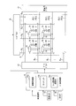
- FIG. 1 is a diagram illustrating a liquid crystal display device according to Embodiment 1 of the present invention.
- the liquid crystal display device 1 according to the present embodiment includes a liquid crystal panel 2 in which the upper side of FIG. 1 is installed as a viewing side (display surface side), and a non-display surface side of the liquid crystal panel 2 (lower side of FIG. 1).
- a backlight device 3 backlight unit
- the liquid crystal panel 2 constitutes a display unit that displays information.
- the liquid crystal panel 2 includes a color filter substrate 4 (TFT substrate) and an active matrix substrate 5 (counter substrate) constituting a pair of substrates.
- the active matrix substrate 5 and the color filter substrate 4 are disposed to face each other, the peripheral portions of both substrates are bonded with a sealing material, and a liquid crystal layer is provided in a region surrounded by the peripheral portions. That is, a liquid crystal layer (not shown) is sandwiched between the color filter substrate 4 and the active matrix substrate 5.
- Polarizing plates 6 and 7 are provided on the outer surfaces of the color filter substrate 4 and the active matrix substrate 5, respectively. Further, the color filter substrate 4 and the active matrix substrate 5 are made of a transparent transparent resin such as a flat transparent glass material or an acrylic resin. Resin films such as TAC (triacetyl cellulose) or PVA (polyvinyl alcohol) are used for the polarizing plates 6 and 7 and correspond to cover at least the effective display area of the display surface provided in the liquid crystal panel 2. It is bonded to the color filter substrate 4 or the active matrix substrate 5.
- TAC triacetyl cellulose
- PVA polyvinyl alcohol
- the active matrix substrate 5 constitutes one of the pair of substrates.
- pixel electrodes and thin film transistors thin film transistors (in accordance with a plurality of pixels included in the display surface of the liquid crystal panel 2) are provided.
- a TFT (Thin Film Transistor) or the like is formed between the liquid crystal layer (details will be described later).
- the switching circuit (semiconductor device) of the present invention including the thin film transistor is provided for each pixel.
- the color filter substrate 4 constitutes the other of the pair of substrates, and the color filter substrate 4 is formed with a color filter, a counter electrode, and the like between the liquid crystal layer (not shown). )
- the liquid crystal panel 2 is provided with an FPC (Flexible Printed Circuit) 8 connected to a control device (not shown) for controlling the drive of the liquid crystal panel 2 and operates the liquid crystal layer in units of pixels.
- FPC Flexible Printed Circuit
- the display surface is driven in units of pixels and a desired image is displayed on the display surface.
- the liquid crystal mode and pixel structure of the liquid crystal panel 2 are arbitrary. Moreover, the drive mode of the liquid crystal panel 2 is also arbitrary. That is, as the liquid crystal panel 2, any liquid crystal panel that can display information can be used. Therefore, the detailed structure of the liquid crystal panel 2 is not shown in FIG.
- the backlight device 3 includes a light emitting diode 9 as a light source, and a light guide plate 10 disposed to face the light emitting diode 9. Further, in the backlight device 3, the light emitting diode 9 and the light guide plate 10 are sandwiched by the bezel 14 having an L-shaped cross section in a state where the liquid crystal panel 2 is installed above the light guide plate 10. A case 11 is placed on the color filter substrate 4. Thus, the backlight device 3 is assembled to the liquid crystal panel 2 and is integrated as a transmissive liquid crystal display device 1 in which illumination light from the backlight device 3 is incident on the liquid crystal panel 2.
- the light guide plate 10 for example, a synthetic resin such as a transparent acrylic resin is used, and light from the light emitting diode 9 enters.
- a reflection sheet 12 is installed on the opposite side (opposite surface side) of the light guide plate 10 to the liquid crystal panel 2.
- an optical sheet 13 such as a lens sheet or a diffusion sheet is provided on the liquid crystal panel 2 side (light emitting surface side) of the light guide plate 10, and the inside of the light guide plate 10 has a predetermined light guide direction (left side in FIG. 1). The light from the light emitting diode 9 guided in the direction from the right side to the right side is changed to the planar illumination light having uniform luminance and applied to the liquid crystal panel 2.
- the present embodiment is not limited to this, and a direct type backlight device is used. May be.
- a backlight device having other light sources such as a cold cathode fluorescent tube and a hot cathode fluorescent tube other than the light emitting diode can also be used.
- FIG. 2 is a diagram for explaining the configuration of the liquid crystal panel shown in FIG. 2,
- the liquid crystal display device 1 includes a panel control which is an example of a display control unit that performs drive control of the liquid crystal panel 2 (FIG. 1) as the display unit that displays information such as characters and images.
- a source driver 16 and a gate driver 17 that operate based on an instruction signal from the panel control unit 15.
- the liquid crystal display device 1 is provided with a capacitor driver 21 that outputs a predetermined signal to a plurality of capacitors described later. Similar to the source driver 16 and the gate driver 17, the capacitor driver 21 operates based on an instruction signal from the panel control unit 15.
- the panel control unit 15 is provided in the control device, and receives a video signal from the outside of the liquid crystal display device 1. Further, the panel control unit 15 includes a detection result from the temperature sensor TS that detects the ambient temperature of the liquid crystal panel 2 and a detection result from the optical sensor OS that detects the magnitude of external light incident on the liquid crystal panel 2. Is entered.
- the temperature sensor TS and the optical sensor OS are examples of sensors that detect the surrounding environment of the liquid crystal panel (display unit) 2.
- the panel control unit 15 performs predetermined image processing on the input video signal to generate each instruction signal to the source driver 16 and the gate driver 17, and the input video signal.
- a frame buffer 15b capable of storing display data for one frame included, and a signal adjustment unit 15c for adjusting the frame frequency of a display image displayed on the liquid crystal panel 2 are provided. Then, the panel control unit 15 performs drive control of the source driver 16 and the gate driver 17 according to the input video signal, so that information according to the video signal is displayed on the liquid crystal panel 2.
- the signal adjustment unit 15c is configured to adjust the frame frequency based on the detection results of the temperature sensor TS and the optical sensor OS (details will be described later).
- the signal adjustment unit 15c adjusts the voltage of the capacitor controlled by the capacitor driver instead of the frame frequency or in addition to the frame frequency based on the detection results of the temperature sensor TS and the optical sensor OS.
- the frame frequency or the voltage of the capacitor may be adjusted based on the detection results of the temperature sensor TS and the optical sensor OS and the input video signal.
- the source driver 16, the gate driver 17, and the capacitor driver 21 are installed on the active matrix substrate 5. Specifically, the source driver 16 is installed on the surface of the active matrix substrate 5 along the lateral direction of the liquid crystal panel 2 in the outer region of the effective display area A of the liquid crystal panel 2 which is an example of the display panel. ing. Further, the gate driver 17 is installed on the surface of the active matrix substrate 5 so as to be along the vertical direction of the liquid crystal panel 2 in the outer region of the effective display region A. In addition, the capacitor driver 21 is installed on the surface of the active matrix substrate 5 so as to face the gate driver 17 so as to be along the vertical direction of the liquid crystal panel 2 in the outer region of the effective display region A. .
- the configurations of the source driver 16, the gate driver 17, and the capacitor driver 21 are not limited to the above example. For example, at least two of these may be provided concentrated on one side of the effective display area A.
- the source driver 16 and the gate driver 17 are drive circuits that drive a plurality of pixels P provided on the liquid crystal panel 2 side by pixel, and the source driver 16 and the gate driver 17 include a plurality of source electrode lines SL1.
- ⁇ SLm (m is an integer of 2 or more, hereinafter collectively referred to as "SL") and a plurality of gate electrode wirings GL1 to GLn (n is an integer of 2 or more, hereinafter collectively referred to as "GL").
- SL source electrode lines
- GL gate electrode wirings GL1 to GLn
- the source electrode wiring SL and the gate electrode wiring GL constitute a data wiring (signal line) and a scanning wiring (scanning line), respectively, and are made of a transparent glass material or a transparent synthetic resin contained in the active matrix substrate 5.
- the source electrode wiring SL is provided on the substrate so as to be parallel to the matrix column direction (vertical direction of the liquid crystal panel 2), and the gate electrode wiring GL is arranged in the matrix row direction (the liquid crystal panel 2). In the horizontal direction) on the base material.
- the first capacitor lines CSL11 to CSL1n (n is an integer of 2 or more, hereinafter collectively referred to as “CSL1”) and the second capacitor lines CSL21 to CSL2n (hereinafter “ CSL2 ′′ is generally named).
- the first capacitor lines CSL11 to CSL1n are provided in parallel with the second capacitor lines CSL21 to CSL2n, respectively.
- CSL1 and CSL2 are indicated by a single line for the sake of simplicity.
- the first capacitor line CSL1 and the second capacitor line CSL2 are connected to the capacitor driver 21.
- the first capacitor line CSL1 is connected to the pixel electrode of each pixel via the first capacitor.
- the second capacitor line CSL2 is connected via a second capacitor to a connection point between a plurality of thin film transistors connected in series in the switching circuit 18 of each pixel (details will be described later).
- a switching circuit 18 for a pixel electrode (that is, a pixel driving circuit) using the semiconductor device of this embodiment is connected to the switching circuit 18.
- the pixel P having the pixel electrode 19 formed is provided.
- the common electrode 20 is configured to face the pixel electrode 19 with the liquid crystal layer provided on the liquid crystal panel 2 interposed therebetween. That is, in the active matrix substrate 5, the switching circuit 18, the pixel electrode 19, and the common electrode 20 are provided for each pixel.
- the switching circuit 18 has a configuration in which the source and drain of a plurality of thin film transistors are connected in series, and the source electrode wiring SL and the pixel electrode 19 are connected.
- the gates of the plurality of thin film transistors are respectively connected to the gate electrode wiring GL.
- Connection points (nodes) on the plurality of thin film transistors and the pixel electrode side are connected to the first capacitor wiring CSL1 through the first capacitor.
- a connection point between adjacent thin film transistors among the plurality of thin film transistors is connected to the second capacitor wiring CSL2 via the second capacitor.
- at least one of the plurality of thin film transistors of the switching circuit 18 is provided with a light shielding film that blocks light from the backlight. An increase in leakage current of the thin film transistor is suppressed by the light shielding film.
- the switching circuit 18 when a voltage sufficient to cause conduction between the source and the drain is applied to the gates of the plurality of thin film transistors through the gate electrode wiring GL, the source electrode wiring SL, the pixel electrode, and the first electrode The capacitor is electrically connected. Accordingly, when the plurality of thin film transistors are turned on, the pixel electrode and the first capacitor are charged to a predetermined voltage applied from the source electrode line SL. After that, when the gate voltage applied from the gate electrode wiring GL changes and the source and drain of the plurality of thin film transistors become non-conductive (OFF), the source electrode wiring SL, the pixel electrode, and the first capacitor are electrically connected. However, the voltage charged in the pixel electrode and the first capacitor is held.
- the capacitance value of the second capacitor is smaller than the capacitance value of the first capacitor, the drain potential and the source potential of the thin film transistor between the connection point of the first capacitor and the connection point of the second capacitor are Since they are not the same potential, a potential difference occurs. Therefore, in the voltage holding period of the pixel electrode, a voltage is applied through the second capacitor wiring CSL2 so that the potential difference approaches 0. Thereby, the voltage fluctuation of the pixel electrode due to the leakage current is suppressed.
- the gate driver 17 scans the thin film transistors of the corresponding switching circuit 18 with respect to the gate electrode wirings GL1 to GLn based on the instruction signal from the image processing unit 15a. (Gate signal) can be output sequentially. Based on the instruction signal from the image processing unit 15a, the source driver 16 outputs a data signal (voltage signal (gradation voltage)) corresponding to the luminance (gradation) of the display image to the corresponding source electrode wirings SL1 to SLm. can do.
- a data signal voltage signal (gradation voltage)
- the capacitor driver 21 has the first capacitor and the second capacitor in the voltage holding period of the pixel electrode for the capacitor lines CSL11 to CSL1n and CSL21 to CSL2n based on the instruction signal from the image processing unit 15a. A signal for controlling the voltage can be supplied.
- a plurality of pixel P regions are formed in each region partitioned in a matrix by the source electrode wiring SL and the gate electrode wiring GL.
- the plurality of pixels P include red (R), green (G), and blue (B) pixels. These RGB pixels are sequentially arranged in this order, for example, in parallel with the gate electrode lines GL1 to GLn. Further, these RGB pixels can display corresponding colors by a color filter layer (not shown) provided on the color filter substrate 4 side.
- the green pixel can display a green color by arranging a green color filter in a region corresponding to the green pixel of the counter substrate.
- red and blue color filters can be displayed by arranging red and blue color filters in regions corresponding to the respective pixels of the counter substrate.
- the green pixel, the red pixel, and the blue pixel constitute one pixel unit with three colors, thereby enabling color display of an arbitrary color.
- the liquid crystal display device 1 includes a display area formed of a plurality of pixels arranged in a matrix and a driver for driving the display pixels.
- This driver may be formed on the active matrix substrate at the same time, or may be mounted and connected via a terminal region as a driver chip.
- the alignment direction of the liquid crystal material of the liquid crystal layer is controlled for each pixel by turning on and off the thin film transistor.
- the light transmittance of the backlight is controlled for each pixel.
- the transmittance of the backlight light is controlled for each red pixel, green pixel, and blue pixel.
- An image can be displayed on the liquid crystal display panel by displaying the pixel unit with an arbitrary intensity and display color.
- FIG. 3 is a circuit diagram showing an example of an equivalent circuit of the semiconductor device used in the switching circuit 18 shown in FIG.
- the switching circuit 18 includes a first thin film transistor T1 and a second thin film transistor T2 connected in series.
- a MIS (Metal-Insulator-Semiconductor) type transistor can be used for each thin film transistor T1 and T2.
- One end sides of these thin film transistors T1 and T2 are connected to a pixel electrode which is one electrode of the liquid crystal capacitance Clc.
- the liquid crystal capacitor Clc is formed between the pixel electrode and the common electrode COM facing the pixel electrode.
- the other end sides of the thin film transistors T1 and T2 are connected to the source electrode wiring SL.
- the switching circuit 18 further includes a first capacitor Cs1 having one electrode connected to the one end and the other electrode connected to the first capacitor line CSL1.
- the switching circuit 18 includes a second capacitor Cs2 in which one electrode is connected between the adjacent thin film transistors T1 and T2, and the other electrode is connected to the second capacitor line CSL2. That is, the first capacitor Cs1 connected to the pixel electrode side of the thin film transistors T1 and T2 and the second capacitor Cs2 connected between the thin film transistors T1 and T2 are connected to different capacitor lines CSL1 and CSL2, respectively. It becomes the composition. With this configuration, the voltage (Vop) between the two thin film transistors T1 and T2 can be controlled by the signal of the second capacitor wiring CSL2.
- the first capacitor line CSL1 and the second capacitor line CSL2 are two lines whose voltages are controlled independently. Note that the first capacitor wiring can be simply referred to as “first wiring”, and the second capacitor wiring can be referred to as “second wiring” different from the first wiring.
- the voltage value applied to CSL2 is changed at least once during the pixel voltage holding period of the frame period.
- the value of the voltage applied to the capacitor wiring CSL2 is increased by a certain amount three times during one holding period. That is, the voltage of the capacitor line CSL2 is set so that the voltage Vop on the capacitor Cs2 side becomes higher than the voltage Vpix on the capacitor Cs1 side during the holding period in which the source-drain of the thin film transistor T2 between the two capacitors Cs1 and Cs2 is OFF. It is changing.
- the voltage Vop on the side of the capacitor Cs2 is lower than the voltage Vpix on the side of the capacitor Cs1 before the voltage of the capacitor line CSL2 is changed, and the voltage is changed at such a timing that it becomes higher after the voltage change.
- the voltage change of the capacitor wiring CSL2 during the holding period is performed a plurality of times at regular intervals, and the voltage change amount at each time is equal.
- the voltage of the capacitor wiring CSL2 can be controlled using the time interval and the voltage change amount as parameters, and the adjustment becomes easy.
- the direction of change (increase or decrease) of the voltage applied to the capacitor wiring CSL2 during the holding period changes the voltage in a direction in which the potential difference between Vop and Vpix decreases, that is, the potential difference approaches 0. It is preferable.
- control can be performed so that Vop> Vpix immediately after changing the voltage applied to CSL2 during the holding period.
- the charge held in the pixel electrode is only lost during the holding period, but by controlling as in this embodiment, the charge can be supplied to the pixel portion for a certain period during the holding period. It becomes possible.
- the amount and timing of changing the voltage of the capacitor wiring CSL2 in the holding period can be appropriately set according to the characteristics of the switching circuit 18.
- the amount ⁇ CSL2 for changing the voltage of the capacitor wiring CSL2 during the holding period can be calculated using the following equation (1) as an example.
- Cop represents the total sum of the capacitances connected to the node indicated by Vop in FIG. 3 (the node on the line connecting the thin film transistors T1 and T2).
- Cop can be, for example, the sum of Cs2, the gate-drain capacitance of the transistor T1, the gate-source capacitance of the transistor T2, and the parasitic capacitance between each signal wiring (SL, GL, CSL1) and the node.
- Cs2 in the above formula (1) represents the capacitance of the second capacitor Cs2 shown in FIG.
- the voltage value of Vop that changes with time can be reset. Therefore, it is possible to prevent the voltage value of Vop from being separated from the voltage value of Vpix with time and the Vds of the thin film transistor T2 is increased, thereby increasing the off-leakage current. Therefore, it is possible to hold the pixel voltage for a longer time than when this drive is not performed, and it is possible to drive at an extremely low drive frequency. As a result, low power consumption of the display device can be realized.
- a light shielding film is disposed on the thin film transistors T1 and T2 of the switching circuit 18.
- the light-shielding film is preferably provided at a position where the illumination light of the backlight device 3 is blocked so as not to hit the thin film transistor, for example, at a lower portion of the thin film transistor (on the backlight device 3 side). Further, a light shielding film may be provided over the thin film transistor (on the display surface side).
- the light shielding film can prevent the illumination light of the backlight device 3 or the light from the outside of the liquid crystal panel 2 (external light) from directly reaching the channel portions of the thin film transistors T1 and T2. Thereby, an increase in off-leakage current is suppressed.
- FIG. 5 is a graph showing changes in the off-leakage current of the thin film transistor when the light shielding film is provided and when the light shielding film is not provided.
- the vertical axis represents the off-leakage current value (lds) of the thin film transistor
- the horizontal axis represents the source-drain voltage (Vds) of the thin film transistor.
- the off-leakage current of the thin film transistor is reduced by about two digits by providing the light shielding film.
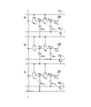
- FIG. 6 is a circuit diagram showing an example of an equivalent circuit of switching circuits arranged in the vertical direction (matrix column direction) of the liquid crystal panel 2 among the switching circuits 18 provided for each pixel in the active matrix substrate 5.
- three switching circuits having the configuration shown in FIG. 3 are arranged in the vertical direction, and these three switching circuits share the source electrode wiring SL extending in the vertical direction.
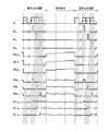
- FIG. 7 is a diagram showing an example of a signal waveform when the circuit shown in FIG. 6 is driven.
- the gate electrode wiring GLn ⁇ 1 is synchronized with the timings 1,..., N ⁇ 1, n, n + 1 indicating the pixel value applied through the source electrode wiring SL in the writing period.
- GLn, GLn + 1 are applied with voltages for turning on the thin film transistors T1n-1, T2n-1, T1n, T2n, T1n + 1, T2n + 1, respectively.
- the source electrode wiring SL when the voltage of the nth pixel value is applied to the source electrode wiring SL, the ON voltage is applied to the gate electrode wiring GLn, and the thin film transistors T1n and T2n are turned on. Accordingly, the source electrode wiring SL and the pixel electrode are brought into conduction in the pixel in the n-th row, and a predetermined voltage corresponding to the pixel value to be displayed in the liquid crystal capacitor Clcn and the first capacitor Cs1n is charged. That is, the voltage Vpixn of the pixel electrode is a voltage corresponding to the pixel value. At this time, a pulse voltage is also applied to the second capacitor wiring CSL2n in the n-th row, and the voltage Vopn between the two thin film transistors T1 and T2 becomes a predetermined voltage.
- the voltage of the (n + 1) th pixel value is applied to the source electrode wiring SL
- the voltage of the gate electrode wiring GLn returns from the ON voltage to the original, and the ON voltage is applied to the gate electrode wiring GLn + 1 in the (n + 1) th row.
- the pixel voltage holding period starts in the pixels in the n-th row.
- the holding period starts after the end of the writing period, but the starting time of the holding period may be recognized in any way, and is not limited to any one.
- voltage application is repeated for all the rows and columns of the matrix.
- the voltage is changed twice in the capacitor wirings CSL21,..., CSL2n-1, CSL2n, CSL2n + 1 at the same timing.
- the voltages Vopn ⁇ 1, Vopn, and Vopn + 1 between the two thin film transistors T1n ⁇ 1 and T2n ⁇ 1, T1n and T2n, T1n + 1, and T2n + 1 are reset. That is, in the holding period, immediately after resetting Vopn ⁇ 1, Vopn, and Vopn + 1, the voltage of the capacitor wiring CSL2 is controlled so that Vop ⁇ Vpix. Due to the voltage change in the holding period of the capacitor wiring CSL2, the fluctuation due to the leakage current of the voltage Vpixn ⁇ 1, Vpixn, Vpixn + 1 of the pixel electrode of each pixel is suppressed.
- FIG. 8 is a diagram showing another example of drive signal waveforms in the circuit shown in FIG.
- the voltage is changed at the same timing in all the capacitor wirings CSL21,... CSL2n-1, CSL2n, CSL2n + 1 even in the writing period.
- the voltage of all the capacitor wirings CSL21,... CSL2n-1, CSL2n, CSL2n + 1 is set to the low level from the start of pixel writing of the first row to the end of pixel writing of the last row, When the pixel writing of the last row is completed, a predetermined level of voltage is applied.
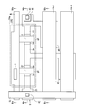
- FIG. 9 is a plan view showing the main structure of the switching circuit.
- FIGS. 10A, 10B, and 10C are a cross-sectional view taken along line VIIa-VIIa, a cross-sectional view taken along line VIIb-VIIb, and a cross-sectional view taken along line VIIc-VIIc in FIG. 9, respectively.
- the silicon layer SC as a semiconductor layer configured in a substantially linear shape is provided below the gate electrodes g ⁇ b> 1 and g ⁇ b> 3 connected to the gate electrode wiring GL. .
- a light shielding film 24b is formed below the silicon layer SC.
- the light shielding film 24b is provided so as to overlap with the gate electrode wiring GL and the direction perpendicular to the paper surface of FIG. 9 (thickness direction of the active matrix substrate 5). That is, the light shielding film 24b is provided below the gate electrodes g1 and g3 of the thin film transistors T1 and T2, and serves as a lower light shielding film that shields the thin film transistors T1 and T2.
- the light shielding film 24b is preferably formed to extend to a region sufficient to block the backlight irradiation light from entering the channel regions 27 and 35 below the gate electrodes g1 and g3 of the thin film transistors T1 and T2. . For this reason, the light shielding film 24b shown in FIG. 9 is formed not only immediately below the channel regions 27 and 35, but also extending directly below and around the channel regions 27 and 35.
- the upper light shielding film 24a is formed above the silicon layer SC.
- the upper light shielding film 24a is provided so as to cover the thin film transistors T1 and T2. Further, the upper light shielding film 24 is electrically connected to the gate electrode wiring GL through the contact 23.
- a low concentration impurity region (LDD region: Lightly : Doped Drain region) 46 for generating the first capacitor Cs1 and a low concentration impurity region 45 for generating the second capacitor Cs2 extend.
- the low-concentration impurity regions 45 and 46 are provided below the capacitance common lines CSL1 and CSL2, respectively, so that a predetermined capacitance is generated.
- a switching circuit 18 is provided on a substrate body 5a made of a glass substrate for each pixel.
- the light shielding film 24b is formed on the substrate body 5a in the region where the switching circuit 18 is formed.
- a base insulating film 47 is formed so as to cover the light shielding film 24 b and the substrate body 5 a, and a silicon layer SC is provided on the base insulating film 47.
- high-concentration regions shown by cross hatching in FIG. 10) 25, 29, and 37 into which N-type impurities such as phosphorus are implanted at a high concentration, and N-type impurities are implanted at a low concentration.
- Low-concentration impurity regions (LDD regions, indicated by dots in FIG. 10) 26, 28, 34, and 36, and channel regions 27 and 35 formed immediately below the gate electrodes g1 and g3, respectively, are provided. .
- the LDD regions 26, 28, 34, and 36 are arranged so as to sandwich the channel regions 27 and 35 from both sides in the longitudinal direction of the silicon layer SC.
- a gate insulating film 48 is formed so as to cover the silicon layer SC, and gate electrodes g 1 and g 3 are formed on the gate insulating film 48. Thereby, the thin film transistors T1 and T2 are formed as N-type transistors.
- An interlayer film 49 is formed on the gate insulating film 48 so as to cover the gate electrodes g1 and g3.
- the source electrode and the drain electrode 44 formed on the source electrode wiring SL are formed on the interlayer film 49.
- the source electrode is connected to the source region 25 provided in the silicon layer SC through the contact hole 42, and the drain electrode 44 is connected to the drain region 37 provided in the silicon layer SL through the contact hole 43. .
- the upper light shielding film 24 a is provided on the interlayer film 49 so as to be in the same layer as the source electrode and drain electrode 44. As shown in FIG. 10B, the upper light shielding film 24a is provided above the gate electrodes g1 and g3 between the source electrode and the drain electrode 44, and the low-concentration impurity regions 26, 28, and 34 are provided. 36 and the channel regions 27 and 35 are shielded from light. That is, the upper light-shielding film 24a can prevent light from the upper side in FIG. 10B from entering the low-concentration impurity regions 26, 28, 34, and 36 and the channel regions 27 and 35.
- a metal such as molybdenum or tungsten is formed on the substrate body 5a by sputtering, and then patterned by photolithography and etching to form the light shielding film 24b.
- the specific thickness of the light shielding film 24b can be about 100 to 200 nm.
- the base insulating film 47 for example, a SiN film and a SiO 2 film are sequentially formed with a thickness of 100 nm by CVD (Chemical Vapor Deposition). Thereafter, an amorphous silicon film having a thickness of 50 nm is formed above the base insulating film 47, and then polysilicon is formed by laser crystallization. Then, boron is doped into this polysilicon as a channel dope for threshold adjustment.
- CVD Chemical Vapor Deposition
- an SiO 2 film having a thickness of 80 nm is formed as a gate insulating film 48 above the polysilicon, and a metal film such as molybdenum or tungsten is formed above the gate insulating film 48 and patterned. Thereby, the gate electrodes g1 and g3 are formed. Then, in order to form the low-concentration impurity regions 26, 28, 34, and 36 using the gate electrodes g1 and g3 as a mask, an N-type impurity such as phosphorus is doped at a low concentration.
- a photoresist for ensuring the length dimension (LDD length) of the low-concentration impurity regions 26, 28, 34, and 36 is formed, and then the source region 25, the drain region 37, and the high-concentration region 29 are formed.
- LDD length length dimension of the low-concentration impurity regions 26, 28, 34, and 36
- the doping amount is adjusted so that the sheet resistance value is about 50 k ⁇ to 150 k ⁇ (for example, 1 ⁇ 10 13 to 10 14 / cm 2 ). .
- This doping amount is doped so as to cancel the previously doped P-type impurity (boron) for channel doping, and N-type low-concentration impurity regions 26, 28, 34, and 36 are formed.
- phosphorus doping of about 1 ⁇ 10 15 / cm 2 is performed so that the sheet resistance value is 1 k ⁇ or less.
- heat treatment is performed at 500 to 600 ° C. for 1 hour in order to activate the impurities. In order to shorten the heat treatment time, for example, heat treatment may be performed at 650 ° C. to 700 ° C. for several minutes using a lamp annealing apparatus.
- an SiO 2 film and an SiN film are formed to a thickness of about 100 nm to 300 nm, respectively, contact holes 42 and 43 are formed for connection with the source electrode and the drain electrode 44, respectively.
- the drain electrode 44 and a wiring metal, such as Al or an alloy thereof, or a laminated film thereof are formed and patterned.
- the liquid crystal display device 1 forms the pixel electrode 19, and therefore, after forming the wiring, a flattening film made of a resin film or the like is formed, and a transparent film that becomes the pixel electrode 19 is formed thereon.
- An electrode for example, ITO
- Al, Ag, or an alloy thereof is formed on the ITO as a reflective electrode.
- the method of forming the thin film transistors T1 and T2 with N-type transistors has been described.
- the thin film transistors T1 and T2 are formed with P-type transistors, the source region 25 and the drain region are formed.
- the impurity for forming 37 may be a P-type impurity such as boron.
- the switching circuit 18 having this structure can be applied to a switching element that requires a low leakage current.
- the light shielding films 24a and 24b are disposed above and below the thin film transistors T1 and T2.
- the light shielding films 24a and 24b are not necessarily provided on both the thin film transistors T1 and T2.
- an increase in leakage current due to light emitted from the backlight can be suppressed.
- a black matrix formed on a color filter substrate is disposed on top of a thin film transistor. By making this black matrix function as an upper light shielding film, the upper light shielding film 24a shown in FIGS. 9 and 10 can be omitted (see the following modification).
- the active matrix substrate 5 has a semiconductor film, a gate insulating film, a gate signal line, a source signal line, an overcoat film, a planarizing film, It has a structure in which a pixel electrode, an alignment film, and the like are stacked.
- the TFT structure may be a bottom gate type in which the gate signal line is located at the lowermost part, or a top gate type in which the gate signal line is located at the upper part after the semiconductor film is formed first.
- the storage capacitor Cs is formed between the capacitor wiring and the drain electrode on the substrate body, the potential fluctuation of the pixel electrode due to the parasitic capacitance or the off-leak current of the TFT can be suppressed.
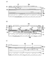
- FIG. 11 is a plan view showing a modification of the main structure of the switching circuit.
- FIGS. 12A, 12B, and 12C are a cross-sectional view taken along line VIIa-VIIa, a cross-sectional view taken along line VIIb-VIIb, and a cross-sectional view taken along line VIIc-VIIc in FIG. 11, respectively.
- the upper light shielding film is omitted.
- the capacitor wiring CSL2 is formed in a layer between the switching circuit and the backlight, and extends below the thin film transistors T1 and T2 and is formed as a light shielding film 24b.
- the capacitor wiring CSL2 is formed to extend below the high concentration region 29 of the silicon layer SC connecting the thin film transistors T1 and T2.
- the second capacitor Cs2 is formed by the high concentration region 29, the capacitor wiring CSL2, and the base insulating film 47 therebetween.
- the high concentration region 29 at the connection portion between the thin film transistors T1 and T2 is wider than the other portions, but the high concentration region 29
- the shape and width are not limited to specific ones.
- the area of the high-concentration region 29 can be designed to have a suitable size in order to secure the second capacitor Cs2 in accordance with the dielectric constant, thickness, and the like of the base insulating film 47.
- the capacitor wiring CSL2 is formed so as to overlap at least the channel regions 27 and 35 of the thin film transistors T1 and T2 and the periphery thereof. As a result, the capacitor wiring CSL2 can also serve as the light shielding film 24b. Further, the capacitor wiring CSL2 is formed to extend linearly along the gate electrode wiring GL. In this manner, by forming the capacitor wiring CSL2 at a position overlapping below the gate electrode wiring GL, it is possible to mitigate the decrease in the aperture ratio due to the capacitor wiring CSL2.
- the capacitor wiring CSL2 also serves as the light shielding film 24b.
- the capacitor wiring CSL1 can also serve as the light shielding film 24b.
- the signal adjustment unit 15c is configured to adjust the frame frequency based on the detection results of the temperature sensor TS and the optical sensor OS.
- the leakage current varies depending on the usage environment of the liquid crystal panel 2, that is, the ambient temperature and external light. Therefore, the signal adjustment unit 15c determines the leakage currents of the thin film transistors T1 and T2 based on the detection results of the temperature sensor TS and the optical sensor OS.
- the signal adjustment unit 15c can reduce the frame frequency within a range in which the display image on the liquid crystal panel 2 does not fluctuate by adjusting the frame frequency based on the determination result of the leak current.
- the signal adjustment unit 15c refers to this data, so that the frame frequency corresponding to the detection result of the sensor Can be determined.
- the signal adjustment unit 15c can adjust the frame frequency to be higher as the temperature detected by the temperature sensor TS is higher. Further, the signal adjustment unit 15c can adjust the frame frequency to be higher as the light detected by the optical sensor OS is stronger.
- the signal adjustment unit 15c can also adjust the change amount and change timing of the voltage applied to the second capacitor Cs2 during the holding period according to the detection result of the sensor. For example, the number of voltage changes (voltage gradation) in the holding period can be changed according to the detection result of the sensor. The higher the temperature detected by the temperature sensor TS or the stronger the light detected by the optical sensor OS, the more the number of times can be adjusted or the amount of change in voltage can be adjusted. Also in this case, similarly, data representing a correspondence relationship between the detection value of the sensor and the amount of change or the number of changes of the voltage applied to the capacitor Cs2 is recorded in advance, and the signal adjustment unit 15c refers to this data. Thus, voltage control of the capacitor Cs2 according to the detection result of the sensor can be executed.
- the signal adjustment unit 15c adjusts the voltage control of the frame frequency and / or the capacitance Cs2 based on each detection result of the sensor and / or the input video signal, so that the liquid crystal panel (display unit) 2
- the voltage control of the frame frequency and / or the capacitance Cs2 of the display image displayed at can be adjusted appropriately.
- the liquid crystal display device 1 having excellent display performance can be easily configured.
- the signal adjustment unit 15c can also adjust the frame frequency and the capacity Cs2 control voltage based on the video signal. For example, when the display image (video signal) is a still image, the signal adjustment unit 15c sets the frame frequency to a low frequency equal to or lower than the predetermined frequency, and when the display image is a moving image, The frequency may be a high frequency equal to or higher than a second predetermined frequency (for example, 50 (Hz)).
- a second predetermined frequency for example, 50 (Hz)
- the signal adjustment unit 15c can reduce the power consumption of the liquid crystal panel (display unit) 2 by adjusting the frame frequency to a predetermined frequency or less according to the input video signal. As a result, the power consumption of the liquid crystal display device 1 can be reduced.
- FIG. 13 is a circuit diagram illustrating an example of an equivalent circuit of the switching circuit according to the second embodiment.
- FIG. 13 shows three switching circuits arranged in the vertical direction among the switching circuits of the active matrix substrate 5.
- the three switching circuits shown in FIG. 13 share the source electrode wiring SL extending in the vertical direction.
- the second capacitor wiring CSL2 of each switching circuit is a gate electrode wiring GL of a switching circuit adjacent in the vertical direction.
- the second capacitor line CSL2n connected to the second capacitor Cs2n of the switching circuit in one row in the matrix of the active matrix substrate 5 is used for the ON / OFF control signals of the thin film transistors T1n + 1 and T2n + 2 of the switching circuit in the adjacent row.
- the gate electrode wiring GLn + 1 is also used.
- the second capacitor Cs2 is connected to the second capacitor line CSL2 that is a dedicated control signal line.
- Cs2n is connected to the next-stage gate electrode wiring GLn + 1.
- FIG. 14 is a diagram showing an example of a signal waveform when the circuit shown in FIG. 13 is driven.
- the gate electrode wirings GLn ⁇ 1, GLn, and GLn + 1 apply voltages for turning on the thin film transistors T1n ⁇ 1, T1n, T1n + 1, T2n ⁇ 1, T2n, and T2n + 1 at the respective write timings.
- a voltage is applied so that the voltages Vopn-2, Vopn-1, and Vopn of the nodes connected via the second capacitors Cs2n-2, CS2n-1, and CS2n in the previous stage are set to predetermined voltages.
- the voltage is changed so that Vop ⁇ Vpix immediately after changing the voltage of CSL2 at one or more gradation voltages.
- the capacitor driver 21 shown in FIG. 2 can be omitted.
- FIG. 15 is a circuit diagram illustrating an example of an equivalent circuit of the switching circuit 18 according to the third embodiment.
- the switching circuit 18 includes a plurality (four in this example) of thin film transistors T1a, T1b, T2a, and T2b connected in series.
- the pixel electrode and the source electrode wiring SL are connected via the source and drain of the plurality of thin film transistors T1a, T1b, T2a, and T2b. That is, the pixel electrode is connected to one end of each of the thin film transistors T1a, T1b, T2a, and T2b, and the source wiring electrode SL is connected to the other end.
- the thin film transistors T1a and T1b form a first switching unit SW1, and the thin film transistors T2a and T2b form a second switching unit SW2.
- One electrode of the first capacitor Cs1 is connected to a connection point between the second switching unit SW2 and the pixel electrode.
- the other electrode of the first capacitor Cs1 is connected to the first capacitor line CSL1.
- One electrode of the second capacitor is connected to a connection point between the first switching unit SW1 and the second switching unit SW2.
- the other electrode of the second capacitor Cs2 is connected to the second capacitor line CSL2.
- the gate electrodes g1, g2, g3, and g4 as the top gate electrodes of the thin film transistors T1a, T1b, T2a, and T2b are connected to the gate electrode wiring GL.
- the thin film transistors T2a and T2b of the second switching unit SW2 are double gate transistors having the top gate electrodes (gate electrodes g3 and g4) and the bottom gate electrode 22, respectively.
- the bottom gate electrode 22 is connected to the bottom gate electrode wiring GL ′.
- the bottom gate electrode 22 one that is integrally formed with respect to the two gate electrodes g3 and g4 can be used.
- the bottom gate electrode 22 can be configured to function also as a (lower) light shielding film that shields illumination light from the backlight device 3.
- the bottom light-shielding film 24b shown in FIGS. 9 and 10A is connected to the bottom gate electrode wiring GL ', so that the bottom gate electrode can also serve as the light-shielding film.
- the thin film transistors T2a and T2b use double gate transistors. Therefore, the current driving force (ON current) of the second switching unit SW2 can be easily increased. In addition, since the on-current can be easily increased in this way, it is possible to easily reduce the charging time for the liquid crystal capacitor CLC.
- a portion of a pixel electrode is a region that transmits light, so that a brighter image is obtained as the ratio of the pixel electrode to the total area of the pixel is larger.
- the gate electrode wiring, the source electrode wiring, and the thin film transistor are arranged in the pixel, the area occupied by the pixel electrode is reduced.
- the opening area tends to be further reduced.
- low-frequency drive circuit technologies for reducing power consumption include a configuration in which a memory function such as a conventional DRAM or SRAM method is added to a pixel, a configuration in which a pixel voltage fresh function is added, and the like.
- a memory function such as a conventional DRAM or SRAM method
- a pixel voltage fresh function is added, and the like.
- full color display is difficult and many elements are added, and the pixel aperture ratio is significantly reduced. Therefore, a low frequency driving technique for realizing a high aperture ratio and full color display is very difficult.
- the pixel circuit in the first and second embodiments has a simple configuration in which the pixel circuit is further provided with the light shielding film, the capacitor Cs2, and the capacitor wiring CSL2, so that a high aperture ratio can be realized.
- the voltage value of the Vop shown in FIG. 3 can be suppressed by changing the voltage value of the signal applied to the CSL2 once or more during the pixel voltage holding period.
- fluctuations in the pixel voltage can be suppressed, and low frequency driving can be realized.
- a full color display can be realized. That is, according to the above-described embodiment, it is possible to realize a display that simultaneously satisfies three of the low-frequency driving, the full-color display, and the high aperture ratio, which have been conventionally considered difficult.
- the semiconductor device of the present invention includes a plurality of switching elements connected in series, one electrode connected to one end side of the plurality of switching elements, and the other electrode connected to the first capacitor wiring.
- 1 capacitor, a second capacitor in which one electrode is connected between adjacent switching elements among the plurality of switching elements, and the other electrode is connected to a second capacitor wiring, and the plurality of switching elements There is no limitation as long as it includes a light shielding film that blocks light incident on at least one of the above.
- various display devices such as transflective or reflective liquid crystal panels or organic EL (Electronic Luminescence) elements, inorganic EL elements, field emission displays, and active matrix substrates used therefor Etc.
- the semiconductor device of the present invention can be applied to a switching circuit used in a peripheral circuit such as a driver circuit. Further, the number of switching units connected in series is not limited to the above two to three.
- the switching element of the present invention is not limited to this, for example, an N-type transistor.
- a transistor and a P-type transistor connected in parallel can be used as one switching element.
- the configuration of the switching unit can be simplified, and the semiconductor device can be easily manufactured. It is preferable in that it can be configured.
- the signal adjustment unit has been described with respect to the configuration in which the frame frequency is adjusted using either the detection results of the temperature sensor and the optical sensor or the input video signal.
- the present invention is not limited to this, and any method may be used as long as the frame frequency is adjusted based on at least one of the detection result from the sensor that detects the state of the surrounding environment of the display unit and the input video signal. That is, the signal adjustment unit of the present invention is based on the input video signal in addition to the detection result of the ambient temperature of the display unit from the temperature sensor and the detection result of the external light from the optical sensor to the display unit.
- the frame frequency may be adjusted appropriately by discriminating the magnitude of the leak current at.
- the upper light-shielding film is composed of a conductor and electrically connected to the gate electrode wiring.
- the upper light-shielding film of the present invention is not limited to this. Without being electrically connected to the electrode wiring, the upper light-shielding film may be in a floating state, or the upper light-shielding film may be constituted by a nonconductor.
- the upper light shielding film is formed in the same layer as the source electrode and the drain electrode as in each of the above embodiments, it is preferable that the upper light shielding film is electrically connected to the gate electrode wiring.
- the capacitor of the present invention is limited to this.
- a channel region can be used instead of the low concentration impurity region.
- top gate electrode structure transistor is used
- a bottom gate electrode structure (reverse stagger structure) transistor may be used, and the light shielding film in this case is formed above the transistor.
- This transistor may be a microcrystalline silicon or amorphous silicon transistor as well as a polycrystalline silicon transistor.
- the bottom gate electrode is used as the (lower) light shielding film
- the present invention is not limited to this.
- the bottom gate electrode may be formed using a transparent electrode, and a light shielding film may be provided below the bottom gate electrode below the semiconductor layer.
- a light shielding film made of a nonconductor can be used.
- the present invention even when a plurality of switching parts are connected in series and a capacitor is connected to the connection part of the switching part, leakage current can be reliably suppressed, and one end side of the plurality of switching parts This is useful for a semiconductor device capable of suppressing voltage fluctuations in the semiconductor device, an active matrix substrate using the same, and a display device.
Landscapes
- Physics & Mathematics (AREA)
- Engineering & Computer Science (AREA)
- General Physics & Mathematics (AREA)
- Nonlinear Science (AREA)
- Crystallography & Structural Chemistry (AREA)
- Computer Hardware Design (AREA)
- Theoretical Computer Science (AREA)
- Chemical & Material Sciences (AREA)
- Mathematical Physics (AREA)
- Microelectronics & Electronic Packaging (AREA)
- Optics & Photonics (AREA)
- Liquid Crystal (AREA)
- Signal Processing (AREA)
- Multimedia (AREA)
- Liquid Crystal Display Device Control (AREA)
- Control Of Indicators Other Than Cathode Ray Tubes (AREA)
Abstract
La présente invention concerne un dispositif à semi-conducteurs équipé des éléments suivants : une pluralité d'éléments de commutation (T1, T2) connectés en série ; une première capacité (Cs1) ayant une électrode connectée à une extrémité de la pluralité des éléments de commutation (T1, T2) et une autre électrode connectée à un premier câblage de capacité (CSL1) ; une seconde capacité (Cs2) ayant une électrode connectée entre des éléments de commutation (T1, T2) adjacents de la pluralité des éléments de commutation et une autre électrode connectée à un second câblage de capacité (CSL2) ; et un film pare-lumière pour protéger contre la lumière incidente sur au moins un des éléments de commutation (T1, T2).
Priority Applications (1)
| Application Number | Priority Date | Filing Date | Title |
|---|---|---|---|
| US14/113,289 US9318513B2 (en) | 2011-04-28 | 2012-04-20 | Semiconductor device, active matrix board, and display device |
Applications Claiming Priority (2)
| Application Number | Priority Date | Filing Date | Title |
|---|---|---|---|
| JP2011101100 | 2011-04-28 | ||
| JP2011-101100 | 2011-04-28 |
Publications (1)
| Publication Number | Publication Date |
|---|---|
| WO2012147657A1 true WO2012147657A1 (fr) | 2012-11-01 |
Family
ID=47072177
Family Applications (1)
| Application Number | Title | Priority Date | Filing Date |
|---|---|---|---|
| PCT/JP2012/060737 Ceased WO2012147657A1 (fr) | 2011-04-28 | 2012-04-20 | Dispositif à semi-conducteurs, carte matrice active, et dispositif d'affichage |
Country Status (2)
| Country | Link |
|---|---|
| US (1) | US9318513B2 (fr) |
| WO (1) | WO2012147657A1 (fr) |
Families Citing this family (11)
| Publication number | Priority date | Publication date | Assignee | Title |
|---|---|---|---|---|
| KR102173707B1 (ko) * | 2013-05-31 | 2020-11-04 | 삼성디스플레이 주식회사 | 박막 트랜지스터 및 이를 포함하는 유기 발광 표시 장치 |
| EP2860720A1 (fr) * | 2013-10-10 | 2015-04-15 | Nederlandse Organisatie voor toegepast- natuurwetenschappelijk onderzoek TNO | Unité électro-optique, dispositif électro-optique et procédé de fonctionnement d'un dispositif électro-optique |
| CN104600081A (zh) * | 2014-12-31 | 2015-05-06 | 京东方科技集团股份有限公司 | 阵列基板及其制作方法、显示面板、显示装置 |
| KR20160094626A (ko) * | 2015-02-02 | 2016-08-10 | 삼성전자주식회사 | 전자 장치의 이미지 처리 방법 및 이미지 처리 장치 |
| KR102558900B1 (ko) * | 2015-10-23 | 2023-07-25 | 엘지디스플레이 주식회사 | 표시장치와 이의 제조방법 |
| JP6518576B2 (ja) * | 2015-11-27 | 2019-05-22 | 株式会社ジャパンディスプレイ | 表示装置及び表示装置のタッチ検出方法 |
| CN109216373B (zh) * | 2017-07-07 | 2021-04-09 | 京东方科技集团股份有限公司 | 阵列基板及其制备方法 |
| CN110767163B (zh) * | 2019-11-08 | 2021-01-26 | 京东方科技集团股份有限公司 | 一种像素电路及显示面板 |
| CN110910825B (zh) * | 2019-12-10 | 2021-04-02 | 京东方科技集团股份有限公司 | 一种显示面板及显示装置 |
| CN113363277A (zh) * | 2021-05-31 | 2021-09-07 | 深圳市华星光电半导体显示技术有限公司 | 发光器件、显示面板及其制备方法 |
| JP2024077307A (ja) * | 2022-11-28 | 2024-06-07 | 株式会社ジャパンディスプレイ | 半導体装置 |
Citations (9)
| Publication number | Priority date | Publication date | Assignee | Title |
|---|---|---|---|---|
| JPH07333653A (ja) * | 1994-06-02 | 1995-12-22 | Semiconductor Energy Lab Co Ltd | アクティブマトリクス表示装置 |
| JPH0846204A (ja) * | 1994-07-28 | 1996-02-16 | Sharp Corp | 表示装置 |
| JPH08328515A (ja) * | 1995-05-31 | 1996-12-13 | Sharp Corp | 画像表示装置 |
| JP2001091973A (ja) * | 1999-09-27 | 2001-04-06 | Matsushita Electric Ind Co Ltd | 液晶表示素子および液晶表示素子の駆動方法 |
| JP2007140310A (ja) * | 2005-11-21 | 2007-06-07 | Nec Corp | 表示装置及びこれらを用いた機器 |
| JP2009115883A (ja) * | 2007-11-02 | 2009-05-28 | Seiko Epson Corp | 電気光学装置及び電子機器 |
| JP2009145866A (ja) * | 2007-08-30 | 2009-07-02 | Sony Corp | 表示装置およびその駆動方法、電子機器 |
| JP2009224884A (ja) * | 2008-03-13 | 2009-10-01 | Canon Inc | 画像制御装置及び画像出力装置 |
| JP2010122609A (ja) * | 2008-11-21 | 2010-06-03 | Canon Inc | 表示制御装置及び表示制御方法 |
Family Cites Families (10)
| Publication number | Priority date | Publication date | Assignee | Title |
|---|---|---|---|---|
| JPH04251818A (ja) | 1991-01-29 | 1992-09-08 | Toshiba Corp | 液晶表示装置 |
| CN100477247C (zh) | 1994-06-02 | 2009-04-08 | 株式会社半导体能源研究所 | 有源矩阵显示器和电光元件 |
| US20050180083A1 (en) * | 2002-04-26 | 2005-08-18 | Toshiba Matsushita Display Technology Co., Ltd. | Drive circuit for el display panel |
| KR100959775B1 (ko) * | 2003-09-25 | 2010-05-27 | 삼성전자주식회사 | 스캔 드라이버와, 이를 갖는 평판표시장치 및 이의 구동방법 |
| TWI297793B (en) * | 2004-05-21 | 2008-06-11 | Sanyo Electric Co | Liquid crystal display device |
| WO2006098449A1 (fr) * | 2005-03-18 | 2006-09-21 | Sharp Kabushiki Kaisha | Afficheur a cristaux liquides |
| JP4932415B2 (ja) * | 2006-09-29 | 2012-05-16 | 株式会社半導体エネルギー研究所 | 半導体装置 |
| KR101352343B1 (ko) * | 2006-12-11 | 2014-01-15 | 삼성디스플레이 주식회사 | 액정표시장치 |
| EP2093608A4 (fr) * | 2006-12-26 | 2012-02-08 | Sharp Kk | Panneau à cristaux liquides, dispositif d'affichage à cristaux liquides, et dispositif de télévision |
| WO2011083598A1 (fr) * | 2010-01-07 | 2011-07-14 | シャープ株式会社 | Dispositif a semi-conducteurs, substrat a matrice active, et afficheur |
-
2012
- 2012-04-20 WO PCT/JP2012/060737 patent/WO2012147657A1/fr not_active Ceased
- 2012-04-20 US US14/113,289 patent/US9318513B2/en not_active Expired - Fee Related
Patent Citations (9)
| Publication number | Priority date | Publication date | Assignee | Title |
|---|---|---|---|---|
| JPH07333653A (ja) * | 1994-06-02 | 1995-12-22 | Semiconductor Energy Lab Co Ltd | アクティブマトリクス表示装置 |
| JPH0846204A (ja) * | 1994-07-28 | 1996-02-16 | Sharp Corp | 表示装置 |
| JPH08328515A (ja) * | 1995-05-31 | 1996-12-13 | Sharp Corp | 画像表示装置 |
| JP2001091973A (ja) * | 1999-09-27 | 2001-04-06 | Matsushita Electric Ind Co Ltd | 液晶表示素子および液晶表示素子の駆動方法 |
| JP2007140310A (ja) * | 2005-11-21 | 2007-06-07 | Nec Corp | 表示装置及びこれらを用いた機器 |
| JP2009145866A (ja) * | 2007-08-30 | 2009-07-02 | Sony Corp | 表示装置およびその駆動方法、電子機器 |
| JP2009115883A (ja) * | 2007-11-02 | 2009-05-28 | Seiko Epson Corp | 電気光学装置及び電子機器 |
| JP2009224884A (ja) * | 2008-03-13 | 2009-10-01 | Canon Inc | 画像制御装置及び画像出力装置 |
| JP2010122609A (ja) * | 2008-11-21 | 2010-06-03 | Canon Inc | 表示制御装置及び表示制御方法 |
Also Published As
| Publication number | Publication date |
|---|---|
| US9318513B2 (en) | 2016-04-19 |
| US20140048812A1 (en) | 2014-02-20 |
Similar Documents
| Publication | Publication Date | Title |
|---|---|---|
| JP5468612B2 (ja) | 半導体装置、アクティブマトリクス基板、及び表示装置 | |
| WO2012147657A1 (fr) | Dispositif à semi-conducteurs, carte matrice active, et dispositif d'affichage | |
| US20220190003A1 (en) | Thin film transistor substrate and display using the same | |
| CN101174071B (zh) | 液晶显示装置、以及电子设备 | |
| US9059294B2 (en) | Semiconductor device, active matrix substrate, and display device | |
| CN204538024U (zh) | 薄膜晶体管基板 | |
| CN104867936B (zh) | 薄膜晶体管基板及利用该薄膜晶体管基板的显示装置 | |
| WO2011027705A1 (fr) | Dispositif à semi-conducteur, substrat de matrice active et dispositif d'affichage | |
| US7164408B2 (en) | Electro-optical device, method of manufacturing the same, and electronic apparatus | |
| US20040256623A1 (en) | Semiconductor device and its manufacturing method | |
| CN204464287U (zh) | 薄膜晶体管基板 | |
| WO2011074338A1 (fr) | Dispositif semi-conducteur, substrat à matrice active et dispositif d'affichage | |
| CN104867937A (zh) | 薄膜晶体管基板和使用该薄膜晶体管基板的显示装置 | |
| US10845639B2 (en) | Display device | |
| WO2010087049A1 (fr) | Dispositif d'affichage à cristaux liquides | |
| US20120146038A1 (en) | Semiconductor device, active matrix substrate, and display device | |
| US7929095B2 (en) | Liquid crystal display panel | |
| US8466020B2 (en) | Method of producing semiconductor device | |
| JP2006171033A (ja) | 液晶表示装置 | |
| KR101677995B1 (ko) | 반사투과형 액정표시장치 및 그 제조방법 | |
| JP2013250319A (ja) | アクティブマトリクス基板、製造方法、及び表示装置 | |
| JP2002297059A (ja) | ドライバ内蔵型アクティブマトリクス表示装置 | |
| WO2014054487A1 (fr) | Écran à cristaux liquides et son procédé de fabrication |
Legal Events
| Date | Code | Title | Description |
|---|---|---|---|
| 121 | Ep: the epo has been informed by wipo that ep was designated in this application |
Ref document number: 12777695 Country of ref document: EP Kind code of ref document: A1 |
|
| WWE | Wipo information: entry into national phase |
Ref document number: 14113289 Country of ref document: US |
|
| NENP | Non-entry into the national phase |
Ref country code: DE |
|
| 122 | Ep: pct application non-entry in european phase |
Ref document number: 12777695 Country of ref document: EP Kind code of ref document: A1 |
|
| NENP | Non-entry into the national phase |
Ref country code: JP |