WO2012147956A1 - Élément conducteur, procédé de fabrication associé, écran tactile et cellule solaire - Google Patents
Élément conducteur, procédé de fabrication associé, écran tactile et cellule solaire Download PDFInfo
- Publication number
- WO2012147956A1 WO2012147956A1 PCT/JP2012/061464 JP2012061464W WO2012147956A1 WO 2012147956 A1 WO2012147956 A1 WO 2012147956A1 JP 2012061464 W JP2012061464 W JP 2012061464W WO 2012147956 A1 WO2012147956 A1 WO 2012147956A1
- Authority
- WO
- WIPO (PCT)
- Prior art keywords
- conductive layer
- conductive
- group
- conductive member
- metal
- Prior art date
- Legal status (The legal status is an assumption and is not a legal conclusion. Google has not performed a legal analysis and makes no representation as to the accuracy of the status listed.)
- Ceased
Links
Images

Classifications
-
- G—PHYSICS
- G06—COMPUTING OR CALCULATING; COUNTING
- G06F—ELECTRIC DIGITAL DATA PROCESSING
- G06F3/00—Input arrangements for transferring data to be processed into a form capable of being handled by the computer; Output arrangements for transferring data from processing unit to output unit, e.g. interface arrangements
- G06F3/01—Input arrangements or combined input and output arrangements for interaction between user and computer
- G06F3/03—Arrangements for converting the position or the displacement of a member into a coded form
- G06F3/041—Digitisers, e.g. for touch screens or touch pads, characterised by the transducing means
- G06F3/045—Digitisers, e.g. for touch screens or touch pads, characterised by the transducing means using resistive elements, e.g. a single continuous surface or two parallel surfaces put in contact
-
- H—ELECTRICITY
- H01—ELECTRIC ELEMENTS
- H01B—CABLES; CONDUCTORS; INSULATORS; SELECTION OF MATERIALS FOR THEIR CONDUCTIVE, INSULATING OR DIELECTRIC PROPERTIES
- H01B1/00—Conductors or conductive bodies characterised by the conductive materials; Selection of materials as conductors
- H01B1/20—Conductive material dispersed in non-conductive organic material
- H01B1/22—Conductive material dispersed in non-conductive organic material the conductive material comprising metals or alloys
-
- H—ELECTRICITY
- H01—ELECTRIC ELEMENTS
- H01B—CABLES; CONDUCTORS; INSULATORS; SELECTION OF MATERIALS FOR THEIR CONDUCTIVE, INSULATING OR DIELECTRIC PROPERTIES
- H01B5/00—Non-insulated conductors or conductive bodies characterised by their form
- H01B5/14—Non-insulated conductors or conductive bodies characterised by their form comprising conductive layers or films on insulating-supports
-
- H—ELECTRICITY
- H05—ELECTRIC TECHNIQUES NOT OTHERWISE PROVIDED FOR
- H05K—PRINTED CIRCUITS; CASINGS OR CONSTRUCTIONAL DETAILS OF ELECTRIC APPARATUS; MANUFACTURE OF ASSEMBLAGES OF ELECTRICAL COMPONENTS
- H05K1/00—Printed circuits
- H05K1/02—Details
-
- H—ELECTRICITY
- H10—SEMICONDUCTOR DEVICES; ELECTRIC SOLID-STATE DEVICES NOT OTHERWISE PROVIDED FOR
- H10F—INORGANIC SEMICONDUCTOR DEVICES SENSITIVE TO INFRARED RADIATION, LIGHT, ELECTROMAGNETIC RADIATION OF SHORTER WAVELENGTH OR CORPUSCULAR RADIATION
- H10F71/00—Manufacture or treatment of devices covered by this subclass
- H10F71/138—Manufacture of transparent electrodes, e.g. transparent conductive oxides [TCO] or indium tin oxide [ITO] electrodes
- H10F71/1385—Etching transparent electrodes
-
- H—ELECTRICITY
- H10—SEMICONDUCTOR DEVICES; ELECTRIC SOLID-STATE DEVICES NOT OTHERWISE PROVIDED FOR
- H10F—INORGANIC SEMICONDUCTOR DEVICES SENSITIVE TO INFRARED RADIATION, LIGHT, ELECTROMAGNETIC RADIATION OF SHORTER WAVELENGTH OR CORPUSCULAR RADIATION
- H10F77/00—Constructional details of devices covered by this subclass
- H10F77/20—Electrodes
- H10F77/244—Electrodes made of transparent conductive layers, e.g. transparent conductive oxide [TCO] layers
-
- H—ELECTRICITY
- H10—SEMICONDUCTOR DEVICES; ELECTRIC SOLID-STATE DEVICES NOT OTHERWISE PROVIDED FOR
- H10F—INORGANIC SEMICONDUCTOR DEVICES SENSITIVE TO INFRARED RADIATION, LIGHT, ELECTROMAGNETIC RADIATION OF SHORTER WAVELENGTH OR CORPUSCULAR RADIATION
- H10F77/00—Constructional details of devices covered by this subclass
- H10F77/20—Electrodes
- H10F77/244—Electrodes made of transparent conductive layers, e.g. transparent conductive oxide [TCO] layers
- H10F77/251—Electrodes made of transparent conductive layers, e.g. transparent conductive oxide [TCO] layers comprising zinc oxide [ZnO]
-
- H—ELECTRICITY
- H10—SEMICONDUCTOR DEVICES; ELECTRIC SOLID-STATE DEVICES NOT OTHERWISE PROVIDED FOR
- H10P—GENERIC PROCESSES OR APPARATUS FOR THE MANUFACTURE OR TREATMENT OF DEVICES COVERED BY CLASS H10
- H10P95/00—Generic processes or apparatus for manufacture or treatments not covered by the other groups of this subclass
-
- G—PHYSICS
- G06—COMPUTING OR CALCULATING; COUNTING
- G06F—ELECTRIC DIGITAL DATA PROCESSING
- G06F2203/00—Indexing scheme relating to G06F3/00 - G06F3/048
- G06F2203/041—Indexing scheme relating to G06F3/041 - G06F3/045
- G06F2203/04103—Manufacturing, i.e. details related to manufacturing processes specially suited for touch sensitive devices
-
- Y—GENERAL TAGGING OF NEW TECHNOLOGICAL DEVELOPMENTS; GENERAL TAGGING OF CROSS-SECTIONAL TECHNOLOGIES SPANNING OVER SEVERAL SECTIONS OF THE IPC; TECHNICAL SUBJECTS COVERED BY FORMER USPC CROSS-REFERENCE ART COLLECTIONS [XRACs] AND DIGESTS
- Y02—TECHNOLOGIES OR APPLICATIONS FOR MITIGATION OR ADAPTATION AGAINST CLIMATE CHANGE
- Y02E—REDUCTION OF GREENHOUSE GAS [GHG] EMISSIONS, RELATED TO ENERGY GENERATION, TRANSMISSION OR DISTRIBUTION
- Y02E10/00—Energy generation through renewable energy sources
- Y02E10/50—Photovoltaic [PV] energy
- Y02E10/541—CuInSe2 material PV cells
-
- Y—GENERAL TAGGING OF NEW TECHNOLOGICAL DEVELOPMENTS; GENERAL TAGGING OF CROSS-SECTIONAL TECHNOLOGIES SPANNING OVER SEVERAL SECTIONS OF THE IPC; TECHNICAL SUBJECTS COVERED BY FORMER USPC CROSS-REFERENCE ART COLLECTIONS [XRACs] AND DIGESTS
- Y02—TECHNOLOGIES OR APPLICATIONS FOR MITIGATION OR ADAPTATION AGAINST CLIMATE CHANGE
- Y02P—CLIMATE CHANGE MITIGATION TECHNOLOGIES IN THE PRODUCTION OR PROCESSING OF GOODS
- Y02P70/00—Climate change mitigation technologies in the production process for final industrial or consumer products
- Y02P70/50—Manufacturing or production processes characterised by the final manufactured product
Definitions
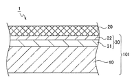
- the electroconductive member which is one Embodiment of this invention has a base material and the electroconductive layer provided on the said base material at least.
- the conductive layer includes a metal nanowire containing a metal element (a) and an average minor axis length of 150 nm or less, and an alkoxide compound of an element (b) selected from the group consisting of Si, Ti, Zr and Al. It contains at least a sol-gel cured product obtained by decomposition and polycondensation.
- the conductive layer satisfies at least one of the following conditions (i) or (ii).
- the metal nanowires included in the conductive layer preferably include silver nanowires from the viewpoint of realizing high conductivity, and have an average minor axis length of 1 nm to 150 nm and an average major axis length of 1 ⁇ m to 100 ⁇ m. It is more preferable to include silver nanowires, and it is further preferable to include silver nanowires having an average minor axis length of 5 nm to 30 nm and an average major axis length of 5 ⁇ m to 30 ⁇ m. Content of the silver nanowire with respect to the mass of all the metal nanowires contained in an electroconductive layer is not restrict
- the step of adding the dispersant is not particularly limited. It may be added before preparing the metal nanowire, and the metal nanowire may be added in the presence of a dispersant, or may be added after the preparation of the metal nanowire for controlling the dispersion state.
- the dispersant include amino group-containing compounds, thiol group-containing compounds, sulfide group-containing compounds, amino acids or derivatives thereof, peptide compounds, polysaccharides, polysaccharide-derived natural polymers, synthetic polymers, or these. And high molecular compounds such as gel.
- various polymer compounds used as a dispersant are compounds included in the polymer described later.
- the electric conductivity and viscosity are measured with the concentration of metal nanowires in the aqueous dispersion being 0.45% by mass.
- concentration of the metal nanowires in the aqueous dispersion is higher than the above concentration, the aqueous dispersion is diluted with distilled water and measured.
- M 1 is Si and a is 4, that is, as tetrafunctional tetraalkoxysilane, for example, tetramethoxysilane, tetraethoxysilane, tetrapropoxysilane, tetrabutoxysilane, methoxytriethoxysilane, ethoxy Examples include trimethoxysilane, methoxytripropoxysilane, ethoxytripropoxysilane, propoxytrimethoxysilane, propoxytriethoxysilane, and dimethoxydiethoxysilane. Of these, tetramethoxysilane, tetraethoxysilane and the like are particularly preferable.
- the content ratio of the sol-gel cured product / metal nanowire is (i) the element (b) selected from the group consisting of Si, Ti, Zr and Al derived from the alkoxide compound as the raw material of the sol-gel cured product.
- the conductive member has a mass ratio (namely, (content of specific alkoxide compound) / (metal nanowire) of the metal nanowire having an average minor axis length of 150 nm or less and the specific alkoxide compound.
- the average film thickness of the conductive layer is calculated as an arithmetic average value obtained by directly measuring the cross section of the conductive layer with an electron microscope and measuring the film thickness of the conductive layer at five points.
- the film thickness of the conductive layer is, for example, a portion where the conductive layer is formed and a portion where the conductive layer is removed using a stylus type surface shape measuring instrument (Dektak (registered trademark) 150, manufactured by Bruker AXS). It can also be measured as a step.
- Dektak registered trademark
- Bruker AXS stylus type surface shape measuring instrument
- acetophenone compound examples include 2,2-dimethoxy-2-phenylacetophenone, 2,2-diethoxyacetophenone, 2- (dimethylamino) -2-[(4-methylphenyl) methyl] -1- [4- (4-morpholinyl) phenyl] -1-butanone, 1-hydroxycyclohexyl phenyl ketone, ⁇ -hydroxy-2-methylphenylpropanone, 1-hydroxy-1-methylethyl (p-isopropylphenyl) ketone, 1-hydroxy- 1- (p-dodecylphenyl) ketone, 2-methyl-1- (4-methylthiophenyl) -2-morpholinopropan-1-one, 1,1,1-trichloromethyl- (p-butylphenyl) ketone, 2 -Benzyl-2-dimethylamino-1- (4-morpholinophenyl) -butanone 1, and the like.
- the content ratio of the metal nanowire (preferably, the metal nanowire having an aspect ratio of 10 or more) is preferably 50% or more on a volume basis with respect to the total amount of the conductive material including the metal nanowire. % Or more is more preferable, and 75% or more is particularly preferable.
- the patterned conductive layer is manufactured, for example, by the following patterning method.
- a non-patterned conductive layer is formed in advance, and a metal nanowire contained in a desired region of the non-patterned conductive layer is irradiated with a high-energy laser beam such as a carbon dioxide laser or a YAG laser, A patterning method in which a part of the metal nanowire is disconnected or disappeared to make the desired region a non-conductive region. This method is described in, for example, Japanese Patent Application Laid-Open No. 2010-44968.
- the method for forming the non-conductive region by applying the etching solution is not particularly limited as long as it is a method for applying the etching solution in a pattern on the conductive layer, and can be appropriately selected according to the purpose.
- screen printing, ink jet printing, a method in which an etching mask is formed in advance by a resist agent, and an etching solution is applied on the coater, roller coating, dipping coating, spray coating, and the like are particularly preferable.
- the ink jet printing for example, either a piezo method or a thermal method can be used.
- the conductive member has high conductivity and transparency in the conductive layer, and has high film strength, excellent wear resistance, and excellent flexibility, for example, touch panel, display electrode, electromagnetic wave shield, organic It is widely applied to EL display electrodes, inorganic EL display electrodes, electronic paper, flexible display electrodes, integrated solar cells, liquid crystal display devices, display devices with touch panel functions, and other various devices. Among these, application to a touch panel and a solar cell is particularly preferable.
- the average film thickness of the conductive layer measured using a stylus type surface shape measuring instrument was 0.065 ⁇ m. Furthermore, the average film thickness of the conductive layer measured using an electron microscope as described below was 0.029 ⁇ m. (Method for measuring film thickness using an electron microscope) After forming a protective layer of carbon and Pt on the conductive member, a slice having a width of about 10 ⁇ m and a thickness of about 100 nm is prepared in a focused ion beam apparatus (trade name: FB-2100) manufactured by Hitachi, Ltd.
- FB-2100 focused ion beam apparatus manufactured by Hitachi, Ltd.
- ⁇ Surface resistivity> The surface resistivity of the conductive region of the conductive layer was measured using Loresta (registered trademark) -GP MCP-T600 manufactured by Mitsubishi Chemical Corporation. The surface resistivity was measured at five locations selected at random in the center of the conductive region of the 10 cm ⁇ 10 cm sample, and the average value was taken as the surface resistivity of the sample.
- the conductive member was subjected to a 20-fold bending test using a cylindrical mandrel bending tester (Cortech Co., Ltd.) equipped with a cylindrical mandrel having a diameter of 10 mm. Surface resistance value after bending test / surface resistance value before bending test) was observed. The presence or absence of cracks was measured visually and using an optical microscope, and the surface resistance value was measured using Loresta-GP MCP-T600 (described above). Flexibility is better as there is no crack and the change in the surface resistance value is smaller (closer to 1).
- the conductive member according to one embodiment of the present invention is excellent in conductivity, transparency (total light transmittance and haze), wear resistance, heat resistance, moist heat resistance and flexibility. I can understand that.
- Conductive member 43 binder composition of conductive member 7 + silver nanowire aqueous dispersion (10)
- Conductive member 44 Binder composition of conductive member 8 + silver nanowire aqueous dispersion (10)
- Conductive member 45 binder constitution of conductive member 9 + silver nanowire aqueous dispersion (10)
- Conductive member 46 Binder composition of conductive member 10 + silver nanowire aqueous dispersion (10)
- Conductive member 47 binder composition of conductive member 15 + silver nanowire aqueous dispersion (10)
- Conductive member 48 Binder composition of conductive member 17 + silver nanowire aqueous dispersion (10)
- Conductive member 49 Binder composition of conductive member 33 + silver nanowire aqueous dispersion (10)
- Conductive member 50 binder composition of conductive member 34 + silver nanowire aqueous dispersion (10)
- Conductive member 51 Binder configuration of conductive member 35 + silver nanowire aqueous dispersion (10)
Landscapes
- Engineering & Computer Science (AREA)
- Physics & Mathematics (AREA)
- General Engineering & Computer Science (AREA)
- Theoretical Computer Science (AREA)
- Chemical & Material Sciences (AREA)
- Spectroscopy & Molecular Physics (AREA)
- Dispersion Chemistry (AREA)
- General Physics & Mathematics (AREA)
- Human Computer Interaction (AREA)
- Microelectronics & Electronic Packaging (AREA)
- Non-Insulated Conductors (AREA)
- Laminated Bodies (AREA)
- Manufacturing Of Electric Cables (AREA)
- Position Input By Displaying (AREA)
- Photovoltaic Devices (AREA)
- Conductive Materials (AREA)
Abstract
La présente invention concerne un élément conducteur qui contient un substrat et une couche conductrice prévue sur le substrat, la couche conductrice contenant : un nanofil métallique qui contient un élément métallique (a) et qui possède une longueur moyenne de petit axe de 150 nm ou moins ; et un matériau durci sol-gel obtenu en soumettant un composé alkoxyde d'un élément (b) sélectionné parmi un groupe constitué de Si, Ti, Zr et Al à une hydrolyse et une polycondensation. En outre, le rapport de la quantité de l'élément (b) contenu dans la couche conductrice par rapport à la quantité de l'élément métallique (a) contenu dans la couche conductrice est dans une plage entre 0,10/1 et 22/1.
Priority Applications (3)
| Application Number | Priority Date | Filing Date | Title |
|---|---|---|---|
| KR1020137028464A KR101675627B1 (ko) | 2011-04-28 | 2012-04-27 | 도전성 부재, 그 제조 방법, 터치 패널 및 태양 전지 |
| CN201280020112.2A CN103503081B (zh) | 2011-04-28 | 2012-04-27 | 导电性构件、其制造方法、触摸屏及太阳电池 |
| US14/062,504 US20140069488A1 (en) | 2011-04-28 | 2013-10-24 | Conductive member, method of producing the same, touch panel, and solar cell |
Applications Claiming Priority (6)
| Application Number | Priority Date | Filing Date | Title |
|---|---|---|---|
| JP2011-102135 | 2011-04-28 | ||
| JP2011102135 | 2011-04-28 | ||
| JP2012-019250 | 2012-01-31 | ||
| JP2012019250 | 2012-01-31 | ||
| JP2012068239 | 2012-03-23 | ||
| JP2012-068239 | 2012-03-23 |
Related Child Applications (1)
| Application Number | Title | Priority Date | Filing Date |
|---|---|---|---|
| US14/062,504 Continuation US20140069488A1 (en) | 2011-04-28 | 2013-10-24 | Conductive member, method of producing the same, touch panel, and solar cell |
Publications (1)
| Publication Number | Publication Date |
|---|---|
| WO2012147956A1 true WO2012147956A1 (fr) | 2012-11-01 |
Family
ID=47072467
Family Applications (1)
| Application Number | Title | Priority Date | Filing Date |
|---|---|---|---|
| PCT/JP2012/061464 Ceased WO2012147956A1 (fr) | 2011-04-28 | 2012-04-27 | Élément conducteur, procédé de fabrication associé, écran tactile et cellule solaire |
Country Status (6)
| Country | Link |
|---|---|
| US (1) | US20140069488A1 (fr) |
| JP (1) | JP5930833B2 (fr) |
| KR (1) | KR101675627B1 (fr) |
| CN (1) | CN103503081B (fr) |
| TW (1) | TWI504702B (fr) |
| WO (1) | WO2012147956A1 (fr) |
Cited By (2)
| Publication number | Priority date | Publication date | Assignee | Title |
|---|---|---|---|---|
| JP2013225467A (ja) * | 2012-03-23 | 2013-10-31 | Fujifilm Corp | 導電性部材およびその製造方法 |
| US20170145737A1 (en) * | 2014-08-27 | 2017-05-25 | Fujifilm Corporation | Heat insulating film, manufacturing method of heat insulating film, heat insulating glass, and window |
Families Citing this family (26)
| Publication number | Priority date | Publication date | Assignee | Title |
|---|---|---|---|---|
| KR102148154B1 (ko) * | 2013-01-22 | 2020-08-26 | 주식회사 동진쎄미켐 | 투명 전도성 막 코팅 조성물, 투명 전도성 막 및 투명 전도성 막의 제조 방법 |
| JP2015018624A (ja) * | 2013-07-09 | 2015-01-29 | 日東電工株式会社 | 透明導電性フィルムおよび透明導電性フィルムの製造方法 |
| KR20150034993A (ko) * | 2013-09-27 | 2015-04-06 | 주식회사 동진쎄미켐 | 금속 나노와이어를 함유하는 전도성 코팅 조성물 및 이를 이용한 전도성 필름의 형성방법 |
| WO2015056445A1 (fr) | 2013-10-16 | 2015-04-23 | 日立化成株式会社 | Fibre conductrice contenant un stratifié, film conducteur photosensible, procédé de fabrication de tracé conducteur, substrat de tracé conducteur et écran tactile |
| WO2015090395A1 (fr) * | 2013-12-19 | 2015-06-25 | Fraunhofer-Gesellschaft zur Förderung der angewandten Forschung e.V. | Electrode à nanofils transparente pourvu d'une couche organique fonctionnelle |
| CN107078151B (zh) * | 2014-01-31 | 2021-05-25 | 英属维尔京群岛商天材创新材料科技股份有限公司 | 包括金属纳米结构复合层的串联有机光伏器件 |
| US9709887B2 (en) * | 2014-03-14 | 2017-07-18 | Hitachi Chemical Company, Ltd. | Photosensitive conductive film |
| EP3706142A1 (fr) * | 2014-03-20 | 2020-09-09 | Cambrios Film Solutions Corporation | Stabilité à la lumière améliorée de conducteurs transparents à base de nanofils |
| JP6371464B2 (ja) * | 2014-04-11 | 2018-08-08 | シーエーエム ホールディング コーポレーション | 銀ナノワイヤーの製造方法 |
| WO2015182745A1 (fr) | 2014-05-30 | 2015-12-03 | 富士フイルム株式会社 | Film thermo-isolant pour fenêtre, matériau thermo-isolant pour fenêtre et fenêtre |
| CN106457747B (zh) * | 2014-05-30 | 2019-11-05 | 富士胶片株式会社 | 窗户用隔热薄膜、窗户用隔热材料及窗户 |
| US9758689B2 (en) * | 2014-10-17 | 2017-09-12 | Xerox Corporation | Silver nanoparticle inks comprising aminomethylsilanes |
| JP6295224B2 (ja) | 2015-03-25 | 2018-03-14 | 富士フイルム株式会社 | 遠赤外線反射フィルム、遠赤外線反射フィルム形成用の分散液、遠赤外線反射フィルムの製造方法、遠赤外線反射ガラスおよび窓 |
| JP2017079114A (ja) * | 2015-10-19 | 2017-04-27 | ユニチカ株式会社 | 金属ナノワイヤー分散液およびそれから得られる透明導電膜 |
| US20170236610A1 (en) * | 2016-02-12 | 2017-08-17 | Tyco Electronics Corporation | Method for Enhancing Adhesion of Silver Nanoparticle Inks Using a Functionalized Alkoxysilane Additive and Primer Layer |
| WO2018030173A1 (fr) * | 2016-08-10 | 2018-02-15 | バンドー化学株式会社 | Composition de liaison et son procédé de préparation |
| WO2018059670A1 (fr) * | 2016-09-27 | 2018-04-05 | Wacker Chemie Ag | Procédé de production des particules de polysilesquioxane sphériques |
| JP6657410B2 (ja) * | 2016-10-06 | 2020-03-04 | ワッカー ケミー アクチエンゲゼルシャフトWacker Chemie AG | 球状ポリシルセスキオキサン粒子の製造方法 |
| KR102019468B1 (ko) | 2016-11-29 | 2019-09-06 | 주식회사 엘지화학 | 반도체용 접착 필름 및 반도체 장치 |
| CN110383118B (zh) | 2017-03-31 | 2021-11-09 | 富士胶片株式会社 | 树脂成型体及蓝光截止层叠体 |
| JP6978227B2 (ja) * | 2017-05-31 | 2021-12-08 | 日東電工株式会社 | 調光フィルム |
| US11188690B1 (en) * | 2017-11-15 | 2021-11-30 | Ansys, Inc. | Systems and methods for performing thermal simulation of an additive manufacturing process |
| CN108008862B (zh) * | 2017-12-19 | 2020-10-23 | 上海天马微电子有限公司 | 触控膜层、触控面板及其触控显示装置 |
| KR102185171B1 (ko) * | 2018-12-04 | 2020-12-01 | 주식회사 디케이티 | 투명전극 디바이스 |
| WO2022054775A1 (fr) * | 2020-09-10 | 2022-03-17 | 互応化学工業株式会社 | Pâte conductrice et film conducteur |
| CN114975516A (zh) * | 2021-02-20 | 2022-08-30 | 宸美(厦门)光电有限公司 | 接触结构及具有所述接触结构的电子装置 |
Citations (5)
| Publication number | Priority date | Publication date | Assignee | Title |
|---|---|---|---|---|
| JPS61183810A (ja) * | 1985-02-07 | 1986-08-16 | 三井東圧化学株式会社 | 透明電極 |
| JP2003151362A (ja) * | 2001-08-31 | 2003-05-23 | Toppan Printing Co Ltd | 導電膜および導電膜の製造方法 |
| JP2009505358A (ja) * | 2005-08-12 | 2009-02-05 | カンブリオス テクノロジーズ コーポレイション | ナノワイヤに基づく透明導電体 |
| JP2011029099A (ja) * | 2009-07-28 | 2011-02-10 | Panasonic Electric Works Co Ltd | 透明導電膜付き基材 |
| JP2011029098A (ja) * | 2009-07-28 | 2011-02-10 | Panasonic Electric Works Co Ltd | 透明導電膜付き基材 |
Family Cites Families (3)
| Publication number | Priority date | Publication date | Assignee | Title |
|---|---|---|---|---|
| JP2005173338A (ja) * | 2003-12-12 | 2005-06-30 | Kinyosha Co Ltd | 導電性部材 |
| US20090052029A1 (en) * | 2006-10-12 | 2009-02-26 | Cambrios Technologies Corporation | Functional films formed by highly oriented deposition of nanowires |
| JP5068298B2 (ja) * | 2009-10-08 | 2012-11-07 | 日揮触媒化成株式会社 | 透明導電性被膜形成用塗布液、透明導電性被膜付基材および表示装置 |
-
2012
- 2012-04-27 CN CN201280020112.2A patent/CN103503081B/zh active Active
- 2012-04-27 WO PCT/JP2012/061464 patent/WO2012147956A1/fr not_active Ceased
- 2012-04-27 KR KR1020137028464A patent/KR101675627B1/ko active Active
- 2012-04-27 TW TW101115228A patent/TWI504702B/zh active
- 2012-04-27 JP JP2012103560A patent/JP5930833B2/ja active Active
-
2013
- 2013-10-24 US US14/062,504 patent/US20140069488A1/en not_active Abandoned
Patent Citations (5)
| Publication number | Priority date | Publication date | Assignee | Title |
|---|---|---|---|---|
| JPS61183810A (ja) * | 1985-02-07 | 1986-08-16 | 三井東圧化学株式会社 | 透明電極 |
| JP2003151362A (ja) * | 2001-08-31 | 2003-05-23 | Toppan Printing Co Ltd | 導電膜および導電膜の製造方法 |
| JP2009505358A (ja) * | 2005-08-12 | 2009-02-05 | カンブリオス テクノロジーズ コーポレイション | ナノワイヤに基づく透明導電体 |
| JP2011029099A (ja) * | 2009-07-28 | 2011-02-10 | Panasonic Electric Works Co Ltd | 透明導電膜付き基材 |
| JP2011029098A (ja) * | 2009-07-28 | 2011-02-10 | Panasonic Electric Works Co Ltd | 透明導電膜付き基材 |
Cited By (2)
| Publication number | Priority date | Publication date | Assignee | Title |
|---|---|---|---|---|
| JP2013225467A (ja) * | 2012-03-23 | 2013-10-31 | Fujifilm Corp | 導電性部材およびその製造方法 |
| US20170145737A1 (en) * | 2014-08-27 | 2017-05-25 | Fujifilm Corporation | Heat insulating film, manufacturing method of heat insulating film, heat insulating glass, and window |
Also Published As
| Publication number | Publication date |
|---|---|
| US20140069488A1 (en) | 2014-03-13 |
| JP5930833B2 (ja) | 2016-06-08 |
| JP2013225461A (ja) | 2013-10-31 |
| CN103503081B (zh) | 2016-11-23 |
| KR20140042798A (ko) | 2014-04-07 |
| TW201249940A (en) | 2012-12-16 |
| CN103503081A (zh) | 2014-01-08 |
| TWI504702B (zh) | 2015-10-21 |
| KR101675627B1 (ko) | 2016-11-11 |
Similar Documents
| Publication | Publication Date | Title |
|---|---|---|
| JP5930833B2 (ja) | 導電性部材、その製造方法、タッチパネル及び太陽電池 | |
| JP5868771B2 (ja) | 導電性部材、その製造方法、タッチパネル及び太陽電池 | |
| WO2013047147A1 (fr) | Composition conductrice, son procédé de production, élément conducteur, écran tactile et cellule solaire | |
| WO2012141058A1 (fr) | Elément conducteur, procédé de fabrication d'élément conducteur, panneau tactile et cellule solaire | |
| JP5646671B2 (ja) | 導電性部材、その製造方法、タッチパネル、及び太陽電池 | |
| WO2012147815A1 (fr) | Élément électroconducteur, son procédé de fabrication, écran tactile et cellule solaire | |
| CN104205247B (zh) | 导电性部件及其制造方法 | |
| WO2013141278A1 (fr) | Composition conductrice, élément conducteur, procédé de fabrication d'élément conducteur, panneau tactile et cellule solaire | |
| WO2013038891A1 (fr) | Elément électroconducteur, procédé de production d'élément électroconducteur, écran tactile et cellule solaire | |
| JP2013201004A (ja) | 導電性パターン部材、その製造方法、タッチパネル及び太陽電池 | |
| JP2013201005A (ja) | 導電性パターン部材の製造方法、導電性パターン部材、タッチパネルおよび太陽電池 | |
| JP2013200997A (ja) | 導電性部材、導電性部材の製造方法、及びタッチパネル | |
| JP5669781B2 (ja) | 導電性部材及びその製造方法、並びにタッチパネル | |
| JP2014036002A (ja) | 導電性部材の形成方法 | |
| JP2013201003A (ja) | 導電性パターン部材、その製造方法、タッチパネル及び太陽電池 | |
| JP2013200998A (ja) | 導電材料の製造方法、並びに、該方法により製造された導電材料及びこれを具備したタッチパネル、タッチパネル機能付き表示装置 |
Legal Events
| Date | Code | Title | Description |
|---|---|---|---|
| 121 | Ep: the epo has been informed by wipo that ep was designated in this application |
Ref document number: 12777407 Country of ref document: EP Kind code of ref document: A1 |
|
| ENP | Entry into the national phase |
Ref document number: 20137028464 Country of ref document: KR Kind code of ref document: A |
|
| NENP | Non-entry into the national phase |
Ref country code: DE |
|
| 122 | Ep: pct application non-entry in european phase |
Ref document number: 12777407 Country of ref document: EP Kind code of ref document: A1 |