WO2012147962A1 - Dispositif d'affichage à cristaux liquides - Google Patents
Dispositif d'affichage à cristaux liquides Download PDFInfo
- Publication number
- WO2012147962A1 WO2012147962A1 PCT/JP2012/061472 JP2012061472W WO2012147962A1 WO 2012147962 A1 WO2012147962 A1 WO 2012147962A1 JP 2012061472 W JP2012061472 W JP 2012061472W WO 2012147962 A1 WO2012147962 A1 WO 2012147962A1
- Authority
- WO
- WIPO (PCT)
- Prior art keywords
- signal line
- wiring
- scanning signal
- scanning
- liquid crystal
- Prior art date
- Legal status (The legal status is an assumption and is not a legal conclusion. Google has not performed a legal analysis and makes no representation as to the accuracy of the status listed.)
- Ceased
Links
Images











Classifications
-
- G—PHYSICS
- G09—EDUCATION; CRYPTOGRAPHY; DISPLAY; ADVERTISING; SEALS
- G09G—ARRANGEMENTS OR CIRCUITS FOR CONTROL OF INDICATING DEVICES USING STATIC MEANS TO PRESENT VARIABLE INFORMATION
- G09G3/00—Control arrangements or circuits, of interest only in connection with visual indicators other than cathode-ray tubes
- G09G3/20—Control arrangements or circuits, of interest only in connection with visual indicators other than cathode-ray tubes for presentation of an assembly of a number of characters, e.g. a page, by composing the assembly by combination of individual elements arranged in a matrix no fixed position being assigned to or needed to be assigned to the individual characters or partial characters
- G09G3/34—Control arrangements or circuits, of interest only in connection with visual indicators other than cathode-ray tubes for presentation of an assembly of a number of characters, e.g. a page, by composing the assembly by combination of individual elements arranged in a matrix no fixed position being assigned to or needed to be assigned to the individual characters or partial characters by control of light from an independent source
- G09G3/36—Control arrangements or circuits, of interest only in connection with visual indicators other than cathode-ray tubes for presentation of an assembly of a number of characters, e.g. a page, by composing the assembly by combination of individual elements arranged in a matrix no fixed position being assigned to or needed to be assigned to the individual characters or partial characters by control of light from an independent source using liquid crystals
- G09G3/3611—Control of matrices with row and column drivers
- G09G3/3674—Details of drivers for scan electrodes
- G09G3/3677—Details of drivers for scan electrodes suitable for active matrices only
-
- G—PHYSICS
- G02—OPTICS
- G02F—OPTICAL DEVICES OR ARRANGEMENTS FOR THE CONTROL OF LIGHT BY MODIFICATION OF THE OPTICAL PROPERTIES OF THE MEDIA OF THE ELEMENTS INVOLVED THEREIN; NON-LINEAR OPTICS; FREQUENCY-CHANGING OF LIGHT; OPTICAL LOGIC ELEMENTS; OPTICAL ANALOGUE/DIGITAL CONVERTERS
- G02F1/00—Devices or arrangements for the control of the intensity, colour, phase, polarisation or direction of light arriving from an independent light source, e.g. switching, gating or modulating; Non-linear optics
- G02F1/01—Devices or arrangements for the control of the intensity, colour, phase, polarisation or direction of light arriving from an independent light source, e.g. switching, gating or modulating; Non-linear optics for the control of the intensity, phase, polarisation or colour
- G02F1/13—Devices or arrangements for the control of the intensity, colour, phase, polarisation or direction of light arriving from an independent light source, e.g. switching, gating or modulating; Non-linear optics for the control of the intensity, phase, polarisation or colour based on liquid crystals, e.g. single liquid crystal display cells
- G02F1/133—Constructional arrangements; Operation of liquid crystal cells; Circuit arrangements
- G02F1/136—Liquid crystal cells structurally associated with a semi-conducting layer or substrate, e.g. cells forming part of an integrated circuit
- G02F1/13606—Liquid crystal cells structurally associated with a semi-conducting layer or substrate, e.g. cells forming part of an integrated circuit having means for reducing parasitic capacitance
-
- G—PHYSICS
- G02—OPTICS
- G02F—OPTICAL DEVICES OR ARRANGEMENTS FOR THE CONTROL OF LIGHT BY MODIFICATION OF THE OPTICAL PROPERTIES OF THE MEDIA OF THE ELEMENTS INVOLVED THEREIN; NON-LINEAR OPTICS; FREQUENCY-CHANGING OF LIGHT; OPTICAL LOGIC ELEMENTS; OPTICAL ANALOGUE/DIGITAL CONVERTERS
- G02F1/00—Devices or arrangements for the control of the intensity, colour, phase, polarisation or direction of light arriving from an independent light source, e.g. switching, gating or modulating; Non-linear optics
- G02F1/01—Devices or arrangements for the control of the intensity, colour, phase, polarisation or direction of light arriving from an independent light source, e.g. switching, gating or modulating; Non-linear optics for the control of the intensity, phase, polarisation or colour
- G02F1/13—Devices or arrangements for the control of the intensity, colour, phase, polarisation or direction of light arriving from an independent light source, e.g. switching, gating or modulating; Non-linear optics for the control of the intensity, phase, polarisation or colour based on liquid crystals, e.g. single liquid crystal display cells
- G02F1/133—Constructional arrangements; Operation of liquid crystal cells; Circuit arrangements
- G02F1/136—Liquid crystal cells structurally associated with a semi-conducting layer or substrate, e.g. cells forming part of an integrated circuit
- G02F1/1362—Active matrix addressed cells
- G02F1/136213—Storage capacitors associated with the pixel electrode
-
- G—PHYSICS
- G02—OPTICS
- G02F—OPTICAL DEVICES OR ARRANGEMENTS FOR THE CONTROL OF LIGHT BY MODIFICATION OF THE OPTICAL PROPERTIES OF THE MEDIA OF THE ELEMENTS INVOLVED THEREIN; NON-LINEAR OPTICS; FREQUENCY-CHANGING OF LIGHT; OPTICAL LOGIC ELEMENTS; OPTICAL ANALOGUE/DIGITAL CONVERTERS
- G02F1/00—Devices or arrangements for the control of the intensity, colour, phase, polarisation or direction of light arriving from an independent light source, e.g. switching, gating or modulating; Non-linear optics
- G02F1/01—Devices or arrangements for the control of the intensity, colour, phase, polarisation or direction of light arriving from an independent light source, e.g. switching, gating or modulating; Non-linear optics for the control of the intensity, phase, polarisation or colour
- G02F1/13—Devices or arrangements for the control of the intensity, colour, phase, polarisation or direction of light arriving from an independent light source, e.g. switching, gating or modulating; Non-linear optics for the control of the intensity, phase, polarisation or colour based on liquid crystals, e.g. single liquid crystal display cells
- G02F1/133—Constructional arrangements; Operation of liquid crystal cells; Circuit arrangements
- G02F1/136—Liquid crystal cells structurally associated with a semi-conducting layer or substrate, e.g. cells forming part of an integrated circuit
- G02F1/1362—Active matrix addressed cells
- G02F1/136286—Wiring, e.g. gate line, drain line
Definitions
- the present invention relates to a liquid crystal display device.
- the inventor determines the time constant of the first wiring arranged on one of the two layers (product of parasitic capacitance and parasitic resistance) and the time constant of the second wiring arranged on the other (parasitic capacitance and parasitic resistance).
- the waveform of the scanning pulse supplied to the scanning signal line connected to the first wiring and the scanning pulse supplied to the scanning signal line connected to the second wiring are different, and the display portion has a horizontal stripe shape. We found a problem that unevenness is likely to appear.
- An object of the present invention is to improve the display quality of a liquid crystal display device that performs three-dimensional wiring in a non-display portion.
- the liquid crystal display device includes first and second scanning signal lines formed in a display portion, first and second wirings formed in a non-display portion, and a scanning signal line driving circuit. Two wirings are formed in different layers, and the scanning signal line driving circuit is connected to the first scanning signal line through the first wiring and is connected to the second scanning signal line through the second wiring, The time constant of the first wiring is smaller than the time constant of the second wiring, and the first scanning pulse output from the scanning signal line driving circuit to the first wiring is first at the end from the active level to the inactive level. An inclined portion is included.
- the first scanning pulse and the second scanning pulse when each of them is supplied to the first and second scanning signal lines via the first and second wirings, the pull-in voltage associated with the deactivation of the first scanning pulse and the deactivation of the second scanning pulse.
- the difference from the pull-in voltage associated with can be reduced.
- horizontal stripe-shaped display unevenness can be suppressed and display quality can be improved.
- the present invention it is possible to improve the display quality of a liquid crystal display device that performs three-dimensional wiring in a non-display portion.
- FIG. 1 is a schematic diagram illustrating a configuration of a liquid crystal display device of Example 1.
- FIG. 2 is a cross-sectional view of the liquid crystal panel of Example 1.
- FIG. 3 is a schematic diagram illustrating a pixel configuration of the liquid crystal display device of Example 1.
- FIG. 3 is a plan view of a liquid crystal panel of Example 1.
- FIG. 6 is a cross-sectional view taken along the line Y-Y ′ of FIG. 5.
- 3 is an equivalent circuit diagram illustrating a pixel configuration of the liquid crystal panel of Example 1.
- FIG. It is a schematic diagram which shows the conventional scanning pulse.
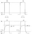
- FIG. 3 is a schematic diagram illustrating scanning pulses of the liquid crystal display device according to the first embodiment.
- 3 is a schematic diagram illustrating a configuration of a gate driver according to Embodiment 1.
- FIG. 10 is a timing chart showing the operation of the gate driver of FIG. 9.
- FIG. 3 is a schematic diagram illustrating another configuration of the gate driver according to the first embodiment. It is a table
- resistor. 12 is a timing chart illustrating an operation of the gate driver of FIG. 11. 12 is a timing chart showing another operation of the gate driver of FIG. 11. 15 is a table showing an example of register input in FIG. 14. 12 is a timing chart showing still another operation of the gate driver of FIG. 17 is a table showing an example of register input in FIG. 16. 12 is a timing chart showing still another operation of the gate driver of FIG. FIG. 19 is a table showing an example of register input in FIG. 18. FIG.
- FIG. 6 is a schematic diagram illustrating a scan pulse setting method (previous two lines) in the first embodiment.
- FIG. 3 is a schematic diagram illustrating a scan pulse setting method (rear two lines) in the first embodiment.
- FIG. 6 is a schematic diagram illustrating an example of setting each scanning pulse in the first embodiment.
- 6 is a schematic diagram illustrating an example of pixel writing polarity (H line inversion) in Embodiment 1.
- FIG. FIG. 6 is a schematic diagram illustrating an example of pixel writing polarity in Example 1 (vertical 1 dot horizontal 1 dot inversion).
- FIG. 6 is a schematic diagram illustrating an example of pixel writing polarity in Example 1 (vertical 2 dots, horizontal 1 dot inversion). 6 is a schematic diagram illustrating an example of pixel writing polarity (V-line inversion) in Embodiment 1.
- FIG. FIG. 6 is a schematic diagram illustrating a configuration of a gate driver according to a second embodiment.
- FIG. 29 is a timing chart showing an operation of the gate driver of FIG. 28.
- FIG. FIG. 10 is a schematic diagram illustrating another configuration of the gate driver according to the second embodiment.
- FIG. 31 is a timing chart showing an operation of the gate driver of FIG. 30.
- FIG. FIG. 31 is a timing chart showing still another operation of the gate driver of FIG. 30.
- FIG. 31 is a timing chart showing still another operation of the gate driver of FIG. 30.
- FIG. 6 is a schematic diagram illustrating a configuration of a liquid crystal display device of Example 3.
- FIG. 6 is a schematic diagram illustrating a pixel configuration and a scan pulse input configuration of a liquid crystal display device of Example 3.
- FIG. 9 is a schematic diagram illustrating a scan pulse setting method (previous two lines) in Example 3.
- FIG. 10 is a schematic diagram illustrating a scan pulse setting method (rear two lines) in the third embodiment.
- FIG. 10 is a schematic diagram illustrating an example of pixel writing polarity (H line inversion) in Example 3.
- FIG. 6 is a schematic diagram illustrating an example of pixel writing polarity in Example 3 (vertical 1 dot horizontal 1 dot inversion).
- FIG. 10 is a schematic diagram illustrating an example of pixel writing polarity in Example 3 (vertical 2 dots, horizontal 1 dot inversion).
- FIG. 10 is a schematic diagram illustrating an example of pixel writing polarity in Example 3 (V-line inversion). It is a schematic diagram which shows one structural example of this liquid crystal display device.
- the term “column direction (the direction perpendicular to the column direction is the row direction)” is used for convenience of description.
- the “column direction” may be the vertical direction or the horizontal direction.
- FIG. 1 is a schematic diagram illustrating the configuration of the liquid crystal display device according to the first embodiment.
- the liquid crystal display device 1 includes a liquid crystal panel 2, a driver 5 in which a scanning signal line driving circuit and a data signal line driving circuit are integrated on one chip, and a display control circuit 4.
- the liquid crystal panel 2 is driven by a driver 5, and the driver 5 is controlled by a display control circuit 4.
- the liquid crystal panel 2 includes an active matrix substrate, a counter substrate (for example, a color filter substrate), and a liquid crystal layer disposed between the two substrates, and a plurality of subpixels are provided in a matrix on the display unit.
- the non-display portion is provided with four wirings Ha (first wiring), Hb (third wiring), Hc (second wiring), and Hd (fourth wiring).
- Each sub-pixel includes a pixel electrode formed on the active matrix substrate, a counter electrode formed on the counter substrate, and a liquid crystal layer between the pixel electrode and the corresponding electrode, and has a plurality of primary colors (for example, red, green, and blue). Display one.
- the pixel electrode of each subpixel is connected to a data signal line through a transistor, and this transistor is connected to a scanning signal line. Note that the data signal lines extend in the column direction, and the scanning signal lines extend in the row direction.
- One pixel is composed of three sub-pixels arranged in the column direction (scanning direction) that display different primary colors (triple scan method).
- the pixel P in FIG. 1 includes R (red) sub-pixels, G (green) sub-pixels, and B (blue) sub-pixels arranged in the column direction.
- the G sub-pixel is driven by the data signal line D and the scanning signal line Gb (third scanning signal line)
- the B sub-pixel is Driven by the data signal line D and the scanning signal line Gc (second scanning signal line).
- the sub pixel (R) adjacent to the downstream side of the B sub pixel in the scanning direction is driven by the data signal line D and the scanning signal line Gd (fourth scanning signal line).
- the scanning signal lines Ga to Gd are arranged in this order along the scanning direction.
- a plurality of sub-pixels arranged in the row direction are driven by the same scanning signal line and display the same primary color.
- a plurality of subpixels included in the same row as the R subpixel of the pixel P are driven by the scanning signal line Ga to display R.
- a plurality of sub-pixels included in the same row as the G sub-pixel of the pixel P are driven by the scanning signal line Gb to display R.
- a plurality of sub-pixels included in the same row as the B sub-pixel of the pixel P are driven by the scanning signal line Gc to display B.
- the scanning signal line Ga is connected to the driver 5 via the wiring Ha
- the scanning signal line Gb is connected to the driver 5 via the wiring Hb
- the scanning signal line Gc is connected to the driver 5 via the wiring Hc.
- the scanning signal line Gd is connected to the driver 5 via the wiring Hd
- the scanning pulse output from the driver 5 is supplied to the scanning signal lines Ga to Gd via the wirings Ha to Hd.
- the display unit of the liquid crystal panel 2 has a rectangular shape surrounded by the first and second short sides E1 and E2 and the four sides of the first and second long sides, and the wirings Ha and Hc have the first short side E1.
- the wirings Hb and Hd pass through the outside of the second short side E2.
- FIG. 2 is a cross-sectional view showing the structure of the active matrix substrate in region X (region surrounded by oblique lines) in FIG.
- a wiring Ha is formed on a transparent substrate (glass substrate) 30 (on the gate layer GL)
- a gate insulating film 21 is formed so as to cover the wiring Ha
- a source insulating film 21 is formed on the gate insulating film 21 (source A wiring Hc is formed on the layer SL
- an inorganic interlayer insulating film 25 is formed so as to cover the wiring Hc
- a thicker organic interlayer insulating film 26 is formed on the inorganic interlayer insulating film 25.
- the wiring Hb is formed in the same layer (gate layer GL) as the wiring Ha
- the wiring Hd is formed in the same layer (source layer SL) as the wiring Hc.
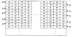
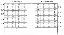
- FIG. 3 shows a corresponding primary color, a formation layer (GL or SL) of a connected wiring, and a via area (outside of the first short side E1 or outside of the second short side E2) for each subpixel row. Let me show you.
- the non-display portion can be reduced (narrow frame).
- FIG. 4 is a plan view of a portion corresponding to the pixel P (see FIG. 1) of the active matrix substrate.
- the pixel electrode 17a of the R sub-pixel, the pixel electrode 17b of the G sub-pixel, and the pixel electrode 17c of the B sub-pixel are arranged in the scanning direction along the data signal line D.
- a scanning signal line Ga is disposed between the electrode 17a and the pixel electrode 17b, and a scanning signal line Gb is disposed between the pixel electrode 17b and the pixel electrode 17c.
- a part of the scanning signal line Ga is a gate electrode of the transistor 12, the source electrode 7 of the transistor 12 is connected to the data signal line D, the drain electrode 8 of the transistor 12 is connected to the drain extraction electrode 27, and the drain extraction The electrode 27 is connected to the pixel electrode 17 a through the contact hole 11. Further, the capacitor electrode 127 formed in the same layer as the data signal line D is connected to the pixel electrode 17a through the contact hole 111, and the capacitor electrode 127 and the storage capacitor wiring 18 overlap with each other through the gate insulating film.
- . 5 is a cross-sectional view taken along the line Y-Y 'of FIG. As shown in FIG.
- the scanning signal line Ga and the storage capacitor line 18 are formed on the transparent substrate (glass substrate) 30, and the gate insulating film 21 is formed so as to cover the scanning signal line Ga and the storage capacitor line 18.
- a data signal line D and a drain lead electrode 27 are formed on the gate insulating film 21, an inorganic interlayer insulating film 25 is formed so as to cover the data signal line D and the drain lead electrode 27, and on the inorganic interlayer insulating film 25,
- a thicker organic interlayer insulating film 26 is formed, and a pixel electrode 17 a is formed on the organic interlayer insulating film 26.
- the inorganic interlayer insulating film 25 and the organic interlayer insulating film 26 are removed, so that the pixel electrode 17a and the drain lead electrode 27 are in contact with each other.
- FIG. 6A is an equivalent circuit diagram of the R subpixel and the B subpixel of the pixel P (see FIG. 1).
- a liquid crystal capacitor CLC is formed between the pixel electrode 17a and the counter electrode COM
- a storage (storage) capacitor CCS is formed between the pixel electrode 17a and the storage capacitor wiring 18, and the pixel electrode 17a
- a parasitic capacitance Cgd is formed between the scanning signal line Ga connected to the wiring Ha.
- the parasitic capacitance Cgd is generated, for example, in an overlapping portion between the scanning signal line Ga and the drain electrode 8 and the drain extraction electrode 27 in FIGS.
- FIG. 6B is an equivalent circuit diagram of the B subpixel of the pixel P (see FIG. 1).
- a liquid crystal capacitor CLC ′ is formed between the pixel electrode 17c and the counter electrode COM, and a storage (storage) capacitor CCS ′ is formed between the pixel electrode 17c and the storage capacitor wiring 18, and the pixel electrode A parasitic capacitance Cgd ′ is formed between 17c and the scanning signal line Gc connected to the wiring Hc.
- the potential V (17a) of the pixel electrode 17a is drawn due to the parasitic capacitance Cgd when the transistor 12 is OFF (at the fall of the scanning pulse GPa supplied to the scanning signal line Ga).
- the potential V (17c) of 17c is drawn due to the parasitic capacitance Cgd 'when the transistor 12' is OFF (at the fall of the scanning pulse GPc supplied to the scanning signal line Gc).
- the pull-in voltage ⁇ va generated in the pixel electrode 17a is generated in the pixel electrode 17c. Is considerably larger than the actual voltage ⁇ vc, it has been found to be a horizontal-striped display unevenness. This is because the time constant of the wiring Ha (connected to the scanning signal line Ga) formed in the gate layer is the time constant of the wiring Hc (connected to the scanning signal line Gc) formed in the metal layer (parasitic capacitance and parasitic resistance). 7 (b), the scanning pulse gpa supplied to the scanning signal line Ga rises more steeply than the scanning pulse gpc supplied to the scanning signal line Gc. Because it goes down.
- the end of the scanning pulse GPa output from the driver 5 to the wiring Ha portion from the active level to the inactive level
- An inclined portion K is provided at each end (portion from the active level to the inactive level) of the scanning pulse GPc to be performed.
- the difference between the pull-in voltage ⁇ va generated in the pixel electrode 17a and the pull-in voltage ⁇ vc generated in the pixel electrode 17c can be reduced (see FIG. 8), and the above-described horizontal stripe-shaped display unevenness can be suppressed. it can.
- the end of the scanning pulse GPb output from the driver 5 to the wiring Hb and the end of the scanning pulse GPd output from the driver 5 to the wiring Hd are each provided with an inclined portion having the same shape as the end of the scanning pulses GPa and GPc. .
- FIG. 9 shows a configuration example of the driver 5 that generates the scanning pulses GPa to GPd including the inclined portion at the end in this way.
- 9 includes a timing controller Tcon, an inverter INV, a P-channel transistor Tp, an N-channel transistor Tn, a gate circuit GC including a shift register (not shown), a level shifter LS, and a potential of VGH.
- the plurality of output ends of the gate circuit GC are connected to the corresponding wirings Ha to Hd, the output end of the level shifter LS is connected to the input end of the inverter INV, and the output end of the inverter INV is the gate terminal of the transistor Tp and the transistor Tn Connected to the gate terminal, the node Nx is connected to the node Ny via the transistor Tp, and the node Nx is connected to one end of the resistor Rx provided outside the driver 5 and provided outside the driver 5. The other end of the resistor Rx is grounded via the transistor Tn, and the node Ny is connected to the output end of a DC-DC converter (not shown) and provided outside the driver 5. It is grounded via the capacitor Cy.
- the potential Vi of the node Nx is supplied to the gate circuit GC, the potential VGH is supplied to the node Ny, the potential VGL is supplied to the gate circuit GC, and the gate clock GCK and the gate start pulse GSP are supplied from the timing controller Tcon to the gate circuit GC. And the slope clock SLCK is supplied from the timing controller Tcon to the level shifter LS.
- FIG. 10 is a timing chart showing the operation of the driver 5 of FIG.
- Each of the gate clock GCK and the slope clock SLCK is composed of the first to fourth periods (the first to third periods are “H” and the fourth period is “L”), and the third period ( H)) and the fourth period (L) of the slope clock SLCK.
- the slope clock SLCK is in the first to third periods (H)
- the transistor Tp in FIG. 9 is turned on
- the transistor Tn is turned off
- the potential Vi VGH supplied to the gate circuit GC
- the capacitor Cx is also charged to VGH. Is done.
- the slope clock SLCK is in the fourth period (L)
- Each stage of the gate circuit GC corresponds to one scanning signal line (wiring), and takes in the gate clock GCK in accordance with the inactivation (falling) of the output (or gate start pulse GSP) of the previous stage, With the activation (rise) of the output of the subsequent stage, the capture of the gate clock GCK is terminated, and Vi is output to the corresponding wiring only during the period when the captured gate clock GCK is “H”, and the other (captured GCK VGL is output to the corresponding wiring during a period when “L” is “L” and when GCK is not captured. As a result, scan pulses GPa to GPd as shown in FIG. 10 are output to the wirings Ha to Hd.
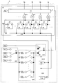
- Another configuration example of the driver 5 is shown in FIG.
- the driver 5 in FIG. 11 includes a timing controller Tcon, a slope destination potential setting circuit SVC, a slope amount setting circuit SRC, a slope clock generation circuit SGC, a slope switch circuit SSC, a gate circuit GC including a shift register, A VGL power source, a potential VSS power source, a potential AVDD power source, a potential VDD power source, a potential VCl power source, and a potential VGH power source (VGL ⁇ VSS ⁇ VDD ⁇ VCl ⁇ AVDD ⁇ VGH).
- VGH is a gate ON voltage
- AVDD is a source analog voltage
- VCI is a driver input voltage (for example, 3.3 V)
- VDD is a logic voltage inside the chip
- VSS is GND
- VGL is a gate OFF voltage.
- a plurality of output ends of the gate circuit GC are connected to the corresponding wirings Ha to Hd, a gate clock GCK and a gate start pulse GSP are supplied from the timing controller Tcon to the gate circuit GC, and a gate is supplied from the timing controller Tcon to the slope clock generation circuit SGC.
- the clock GCK is supplied, and the potential VGL is supplied to the gate circuit GC.
- the slope clock generation circuit SGC sets the slope width according to the input data D0 to D5 to the register RE1 (see FIG. 12A), and further generates the slope clock SLCK using the gate clock GCK.
- the slope clock SLCK is supplied to the slope switch circuit SSC.
- the slope destination potential setting circuit SVC has a node N1, and the node N1 is used as a power source of potential VSS, potential AVDD, potential VDD, or potential VCl according to input data D0 to D1 to the register RE2. Connect (see FIG. 12B).
- the slope switch circuit SSC has nodes N2 to N4, and this node N2 is connected to one of the nodes N3 and N4 according to the slope clock SLCK.
- the node N3 is connected to the power supply of the potential VGH, and the node N4 is connected to the node N1 via the slope amount setting circuit SRC.
- the slope amount setting circuit SRC is a variable resistor, and is set to a resistance value corresponding to the input data D0 to D3 to the register RE3.
- the number of transistors corresponding to the input data is turned on, and resistors equal to the number of turned on transistors are connected in parallel. That is, as the number of ON transistors increases, the resistance decreases and the slope becomes steeper (see FIG. 12C). Then, the potential Vi of the node N2 is supplied to the gate circuit GC.
- FIG. 13 is a timing chart showing the operation of the driver 5 of FIG.
- Each of the gate clock GCK and the slope clock SLCK is composed of the first to fourth periods (the first to third periods are “H” and the fourth period is “L”), and the third period ( H)) and the fourth period (L) of the slope clock SLCK.
- the slope clock SLCK is in the first to third periods (H)
- the slope clock SLCK When the slope clock SLCK is in the fourth period (L), the node N2 and the node N4 of the slope switch circuit SSC are connected, and the potential Vi supplied to the gate circuit GC is changed from VGH to the slope destination potential setting circuit SVC.
- the voltage gradually decreases to the set potential (any one of VSS, AVDD, VDD, VCl, and potential VGH).
- the inclination (potential decrease amount per unit time) is set by the slope amount setting circuit SRC, and becomes steep (inclination increases) as the resistance value of the slope amount setting circuit SRC decreases.
- Each stage of the gate circuit GC corresponds to one scanning signal line (wiring), and takes in the gate clock GCK in accordance with the inactivation (falling) of the output (or gate start pulse GSP) of the previous stage, With the activation (rise) of the output of the subsequent stage, the capture of the gate clock GCK is terminated, and Vi is output to the corresponding wiring only during the period when the captured gate clock GCK is “H”, and the other (captured GCK VGL is output to the corresponding wiring during a period when “L” is “L” and when GCK is not captured. As a result, scan pulses GPa to GPd as shown in FIG. 13 are output to the wirings Ha to Hd.
- the scanning pulses GPa to GPd output to the wirings Ha to Hd have the same waveform, but the present invention is not limited to this.
- the input data D0 to D5 to the register RE1 of the slope clock generation circuit SGC (see FIG. 11) is periodically exchanged to output to the wirings Ha and Hb (small time constant).
- the slopes of the scanning pulses GPa and GPb are made the same as the slopes of the slopes of the scanning pulses GPa and GPb and the slopes of the slopes of the scanning pulses GPc and GPd output to the wirings Hc and Hd (large time constant). Can be made larger than the width of the inclined portion of the scan pulses GPc and GPd.
- the input data D0 to D3 to the register RE3 of the slope amount setting circuit SRC are periodically switched to output to the wirings Ha and Hb (small time constant).
- the slopes of the scan pulses GPa and GPb are made the same with the widths of the slopes of the scan pulses GPa and GPb and the widths of the slopes of the scan pulses GPc and GPd output to the wires Hc and Hd (large time constant) Can be made larger than the inclination of the inclined portion of the scanning pulses GPc and GPd.
- the input data D0 to D5 to the register RE1 of the slope clock generation circuit SGC are periodically switched to output to the wirings Ha and Hb (small time constant).
- the scan pulse GPa / GPb is provided with an inclined portion, and the scan pulse GPc / GPd output to the wirings Hc / Hd (large time constant) is not provided with an inclined portion (the end is substantially the time axis with respect to the time axis). Vertical).
- the scanning pulse GPa is supplied to the scanning signal line Ga corresponding to the R (red) sub-pixel row via the GL wiring (Ha) on the left of the display unit, and the scanning pulse GPb Is supplied to the scanning signal line Gb corresponding to the G (green) sub-pixel row via the GL wiring (Hb) on the right side of the display unit, and the scanning pulse GPc is transmitted to the B (
- the scanning signal line Gc corresponding to the sub-pixel row of blue) is supplied to the scanning signal line Gc, and the scanning pulse GPd is supplied to the scanning signal line Gd corresponding to the sub-pixel row of R (red) via the SL wiring (Hd) on the right of the display unit.
- the shape of the end of the scanning pulses GPa to GPd can be set as follows, for example.
- the input data to the register RE3 of the slope amount setting circuit SRC (see FIG. 11) is D1, and the subpixel row (k is a natural number 4k ⁇ 3) connected to the left GL wiring.
- the predetermined gradation (for example, halftone) is displayed on the second sub-pixel row), and the luminance is measured with the other sub-pixel row being displayed in black, and the result is set as a specified value.
- the input data to the register RE3 is set to D1, and the predetermined gradation is displayed on the sub-pixel row (4k-2nd sub-pixel row) connected to the GL wiring on the right side of the display section, and another sub-pixel row is displayed.
- the luminance is measured with black display, and if it is different from the specified value, the input data to the register RE3 is changed to D2, and the measured value is adjusted to the specified value. Further, as shown in FIG. 22, the input data to the register RE3 is set to D1, and the predetermined gradation is displayed on the sub-pixel row (4k-1th sub-pixel row) connected to the SL wiring on the left side of the display unit. At the same time, the luminance is measured with the other sub-pixel row displayed in black, and if it is different from the specified value, the input data to the register RE3 is changed to D3, and the measured value is adjusted to the specified value.
- the input data to the register RE3 is set to D1, and the predetermined gradation is displayed on the sub-pixel row (4kth sub-pixel row) connected to the SL wiring on the right side of the display portion, and the other sub-pixel rows are black.
- the brightness is measured as a display, and if it is different from the specified value, the input data to the register RE3 is changed to D4, and the measured value is adjusted to the specified value.
- measurement and register settings are performed for the (4k-3) th, (4k-2) th, (4k-1), and 4kth subpixel rows, but the present invention is not limited to this.
- measurement and register setting are performed only for the (4k-3) th and (4k-1) th subpixel rows, and (4k-2)
- the register setting of the first subpixel row is the same as the (4k-3) th subpixel row
- the register setting of the (4k-1) th subpixel row is the same as the (4k-1) th subpixel row. You can also.
- FIG. 24 to 27 are schematic diagrams illustrating examples of the polarity of the signal potential written to each sub-pixel.
- FIG. 24 shows a three-gate line inversion method, in which the signal potential supplied to each data signal line is inverted every 3H (horizontal scanning period) and applied to one of the two data signal lines adjacent to the same horizontal scanning period. The polarity of the signal potential supplied is the same as the polarity of the signal potential supplied to the other.
- FIG. 25 shows a vertical one-dot horizontal one-dot inversion method, in which the signal potential supplied to each data signal line is inverted every 1H (horizontal scanning period), and two data signal lines adjacent to the same horizontal scanning period.
- FIG. 26 shows a vertical 2 dot horizontal 1 dot inversion method, in which the signal potential supplied to each data signal line is inverted every 2H (horizontal scanning period), and two data signal lines adjacent to the same horizontal scanning period. The polarity of the signal potential supplied to one of the two is opposite to the polarity of the signal potential supplied to the other.
- FIG. 27 shows a source line inversion method in which the signal potential supplied to each data signal line is inverted every 1V (vertical scanning period) and supplied to one of two data signal lines adjacent to the same horizontal scanning period. The polarity of the signal potential applied is opposite to the polarity of the signal potential supplied to the other.
- Example 2 In the configuration in which three sub-pixels constituting one pixel are arranged in the column direction (scanning direction), the number of scanning signal lines to be scanned increases (three times that in the configuration in which three sub-pixels are arranged in the row direction). Insufficient charge of the pixel electrode is likely to occur (especially when it is assumed to be used at a low temperature such as an in-vehicle liquid crystal display device). In order to solve this problem, precharge is effective.
- the driver 5 can be configured as shown in FIG. 28 and operated as shown in FIG.
- the gate circuit GC of FIG. 11 is provided with a shift register using a D flip-flop and an AND circuit corresponding to each stage of the shift register.
- the gate clock GCK from the timing controller Tcon is input to the CK terminal of each D flip-flop, and the D terminal of each D flip-flop is connected to the Q (output) terminal in the previous stage, and the Q (output terminal) is in the subsequent stage. Connected to the D terminal.
- the AND of the output of each D flip-flop and the gate clock GCK is input to the output circuit OC, and the potential Vi and the potential VGL of the node N2 are supplied to the output circuit OC.
- the Q terminal of the D flip-flop Fa corresponding to the wiring Ha is connected to the D terminal of the D flip-flop Fb corresponding to the wiring Hb
- the Q terminal of the D flip-flop Fb corresponds to the D flip-flop Fc corresponding to the wiring Hc.
- the output of the D flip-flop Fa and the gate clock GCK are input to the AND circuit Aa
- the output of the D flip-flop Fb and the gate clock GCK are input to the AND circuit Ab.
- the output APa of the circuit Aa and the output APb of the AND circuit Ab are input to the output circuit OC.
- the gate start pulse GSP is input to the D terminal of the first stage D flip-flop.
- each of the gate clock GCK and the slope clock SLCK is composed of the first to fourth periods (the first to third periods are “H” and the fourth period is “L”).
- the third period (H)) and the fourth period (L) of the slope clock SLCK overlap.
- the gate start pulse GSP becomes active twice, the first time is synchronized with a certain cycle of the gate clock GCK (becomes active in the first to fourth periods), and the second is the next of this GCK cycle. Synchronized with the next cycle.
- the slope clock SLCK When the slope clock SLCK is in the fourth period (L), the node N2 and the node N4 of the slope switch circuit SSC are connected, and the potential Vi supplied to the output circuit OC is set from VGH by the slope destination potential setting circuit SVC. Gradually decrease to the applied potential (VSS, AVDD, VDD, and VCl).
- the inclination (potential decrease amount per unit time) is set by the slope amount setting circuit SRC, and becomes steep (inclination increases) as the resistance value of the slope amount setting circuit SRC decreases.
- Each D flip-flop transfers the input of the D terminal to the Q terminal when the gate clock signal GCK rises from “L” to “H”. That is, the output Q of the own stage is activated (rises) at the same time as the output Q of the previous stage is deactivated (falls), and is inactive at the same time as the output Q of the next stage is activated (rises). (Fall down). Then, the output of the AND circuit to which the output Q and GCK of its own stage are input is input to the output circuit OC, and the output circuit OC applies Vi to the corresponding wiring only during the period when the output of the AND circuit is “H”. VGL is output to the corresponding wiring in other cases (period in which the output of the AND circuit of the own stage is “L”).
- scanning pulses GPa to GPd that are activated twice at intervals are output to the wirings Ha to Hd, and the scanning signal lines Ga to Gd are signals corresponding to two lines before. It is precharged by the potential (the same polarity as the signal potential of the main charge). Thereby, the problem of insufficient charging of the pixel electrode can be solved.
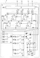
- the driver 5 can be configured as shown in FIG. 30 and operated as shown in FIG.
- the gate circuit GC of FIG. 11 is provided with a two-stage shift register using D flip-flops, and an AND circuit corresponding to each stage of the shift register, and the gate circuit GC is supplied from the timing controller Tcon.
- the gate clocks GCK1 and GCK2 and the gate start pulses GSP1 and GSP2 are supplied to the slope clock generation circuit SGC.
- the tag gate clock GCK1 is input to the CK terminal of the odd-numbered D flip-flop
- the tag gate clock GCK2 is input to the CK terminal of the even-numbered D flip-flop
- the D terminal is connected to the Q (output) terminal of the previous odd-numbered stage
- the Q (output terminal) is connected to the D terminal of the next odd-numbered stage
- the even-numbered D flip-flop is The D terminal is connected to the Q (output) terminal of the previous even numbered stage
- the Q (output terminal) is connected to the D terminal of the next even numbered stage.
- the AND of the odd-stage D flip-flop and the gate clock GCK1 is input to the output circuit OC, and the AND of the even-stage D flip-flop and the gate clock GCK2 is input to the output circuit OC.
- the potential Vi and the potential VGL of the node N2 are supplied to the OC.
- the Q terminal of the D flip-flop Fa corresponding to the wiring Ha is connected to the D terminal of the D flip-flop Fc corresponding to the wiring Hc
- the Q terminal of the D flip-flop Fb is connected to the D flip-flop Fd corresponding to the wiring Hd.
- the output of the D flip-flop Fa and the gate clock GCK1 are input to the AND circuit Aa, and the output of the D flip-flop Fb and the gate clock GCK2 are input to the AND circuit Ab.
- the output APa of the circuit Aa and the output APb of the AND circuit Ab are input to the output circuit OC.
- the gate start pulse GSP1 is input to the D terminal of the first stage D flip-flop F0, and the gate start pulse GSP2 is input to the D terminal of the second stage D flip-flop F0 '.
- each of the gate clocks GCK1 and GCK2 consists of the first to sixth periods (the first to fifth periods are “H” and the sixth period is “L”), and the sixth period ( L) and the third period (H) of GCK2 overlap.
- the slope clock SLCK consists of the first to third periods (the first and second periods are “H” and the third period is “L”).
- the sixth period (L) of GCK1 and the slope clock SLCK The first period (H) overlaps.
- the gate start pulse GSP is activated once in synchronization with a certain cycle of GCK1.
- the slope clock SLCK When the slope clock SLCK is in the third period (L), the node N2 and the node N4 of the slope switch circuit SSC are connected, and the potential Vi supplied to the output circuit OC is set from VGH by the slope destination potential setting circuit SVC.
- the voltage is gradually decreased to the set potential (any one of VSS, AVDD, VDD, VCl, and potential VGH).
- the inclination (potential decrease amount per unit time) is set by the slope amount setting circuit SRC, and becomes steep (inclination increases) as the resistance value of the slope amount setting circuit SRC decreases.
- the odd-numbered D flip-flop shifts the input of the D terminal to the Q terminal, and the even-numbered D flip-flop has the gate clock signal GCK2 of “L”.
- the input of the D terminal is transferred to the Q terminal. That is, the output Q of the own stage is activated (rises) before the output Q of the previous stage is deactivated (falls), and deactivates after the output Q of the next stage is activated (rises). (Fall down). Then, the output of the AND circuit to which the output Q of its own stage and GCK1 or GCK2 are input is input to the output circuit OC.
- the output circuit OC corresponds to Vi only during the period when the output of the AND circuit is “H”.
- VGL is output to the corresponding wiring in other cases (period in which the output of the AND circuit of the own stage is “L”).
- the scan pulses GPa to GPd in which the scan pulse of the own stage overlaps the scan pulse of the previous stage, are output to the wirings Ha to Hd, respectively, and the scan signal lines Ga to Gd correspond to the previous line. Is precharged by the signal potential (the same polarity as the signal potential of the main charge). Thereby, the problem of insufficient charging of the pixel electrode can be solved.
- the scanning pulses GPa to GPd output to the wirings Ha to Hd have the same waveform, but the present invention is not limited to this.
- the input data D0 to D5 to the register RE1 of the slope clock generation circuit SGC are periodically switched to output to the wirings Ha and Hb (small time constant).
- the slopes of the scanning pulses GPa and GPb are made the same as the slopes of the slopes of the scanning pulses GPa and GPb and the slopes of the slopes of the scanning pulses GPc and GPd output to the wirings Hc and Hd (large time constant). Can be made larger than the width of the inclined portion of the scan pulses GPc and GPd.
- the input data D0 to D3 to the register RE3 of the slope amount setting circuit SRC are periodically switched, and output to the wirings Ha and Hb (small time constant).
- the slopes of the scan pulses GPa and GPb are made the same with the widths of the slopes of the scan pulses GPa and GPb and the widths of the slopes of the scan pulses GPc and GPd output to the wires Hc and Hd (large time constant). Can be made larger than the inclination of the inclined portion of the scanning pulses GPc and GPd.
- Example 3 In the above embodiment, the three sub-pixels constituting one pixel are arranged in the column direction (scanning direction), but the present invention is not limited to this. As shown in FIG. 34, these three sub-pixels are arranged in the column direction (perpendicular to the scanning direction). As shown in FIG. 35, the scan pulse GPa is supplied to the scan signal line Ga corresponding to the first sub-pixel row via the SL wiring (Ha) on the left side of the display unit, and the scan pulse GPb is displayed on the display unit.
- the scanning signal GPc is supplied to the scanning signal line Gb corresponding to the second sub-pixel row via the right SL wiring (Hb), and the scanning pulse GPc corresponds to the third sub-pixel row via the GL wiring (Hc) on the left of the display unit.
- the scanning signal GPc may be supplied to the scanning signal line Gc, and the scanning pulse GPd may be supplied to the scanning signal line Gd corresponding to the fourth sub-pixel row via the GL wiring (Hd) on the right side of the display unit.
- the end shape of the scanning pulses GPa to GPd can be set as follows, for example.
- the input data to the register RE3 of the slope amount setting circuit SRC (see FIG. 11) is D1
- the sub-pixel row (k is a natural number 4k ⁇ 3) connected to the left GL wiring.
- the predetermined gradation (for example, halftone) is displayed on the second sub-pixel row), and the luminance is measured with the other sub-pixel row being displayed in black, and the result is set as a specified value.
- the input data to the register RE3 is set to D1, and the predetermined gradation is displayed on the sub-pixel row (4k-2nd sub-pixel row) connected to the GL wiring on the right side of the display section, and another sub-pixel row is displayed.
- the luminance is measured with black display, and if it is different from the specified value, the input data to the register RE3 is changed to D2, and the measured value is adjusted to the specified value.
- the input data to the register RE3 is set to D1, and the predetermined gradation is displayed on the sub-pixel row (4k-1th sub-pixel row) connected to the SL wiring on the left side of the display unit.
- the luminance is measured with the other sub-pixel row displayed in black, and if it is different from the specified value, the input data to the register RE3 is changed to D3, and the measured value is adjusted to the specified value.
- the input data to the register RE3 is set to D1, and the predetermined gradation is displayed on the sub-pixel row (4kth sub-pixel row) connected to the SL wiring on the right side of the display portion, and the other sub-pixel rows are black.
- the brightness is measured as a display, and if it is different from the specified value, the input data to the register RE3 is changed to D4, and the measured value is adjusted to the specified value.
- FIGS. 38 to 41 are schematic diagrams showing examples of the polarity of the signal potential written to each sub-pixel in the configuration of FIGS.
- FIG. 38 shows a one-gate line inversion method in which the signal potential supplied to each data signal line is inverted every 3H (horizontal scanning period) and is applied to one of two data signal lines adjacent to the same horizontal scanning period. The polarity of the signal potential supplied is the same as the polarity of the signal potential supplied to the other.
- FIG. 39 shows a vertical 1-dot horizontal 1-dot inversion method, in which the signal potential supplied to each data signal line is inverted every 1H (horizontal scanning period), and two data signal lines adjacent to the same horizontal scanning period.
- FIG. 40 shows a vertical 2 dot horizontal 1 dot inversion method, in which the signal potential supplied to each data signal line is inverted every 2H (horizontal scanning period), and two data signal lines adjacent to the same horizontal scanning period are displayed. The polarity of the signal potential supplied to one of the two is opposite to the polarity of the signal potential supplied to the other.
- FIG. 41 shows a source line inversion method in which the signal potential supplied to each data signal line is inverted every 1V (vertical scanning period) and supplied to one of two data signal lines adjacent to the same horizontal scanning period. The polarity of the signal potential applied is opposite to the polarity of the signal potential supplied to the other.
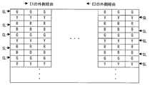
- the primary colors of the sub-pixels are four colors of red (R), green (G), blue (B), and Y (yellow). Is connected to the wiring passing through the outside of the first short side E1, and the scanning signal line corresponding to the yellow subpixel is formed in the gate layer GL.
- the scanning signal line corresponding to the red sub-pixel is connected to the wiring passing through the outside of the short side E2, and connected to the wiring passing through the outside of the first short side E1 to the blue sub-pixel.
- the corresponding scanning signal line may be formed in the source layer SL and connected to the wiring passing through the outside of the second short side E2. In this way, in the entire display unit, sub-pixels of the same color (particularly G or Y) are connected to wiring on the same layer and the same side (with respect to the display unit) via the scanning signal lines. It is easy to set the waveform of the scan pulse output to the wiring.
- the liquid crystal display device includes first and second scanning signal lines formed in a display portion, first and second wirings formed in a non-display portion, and a scanning signal line driving circuit. Two wirings are formed in different layers, and the scanning signal line driving circuit is connected to the first scanning signal line through the first wiring and is connected to the second scanning signal line through the second wiring, The time constant of the first wiring is smaller than the time constant of the second wiring, and the first scanning pulse output from the scanning signal line driving circuit to the first wiring is first at the end from the active level to the inactive level. An inclined portion is included.
- the first scanning pulse and the second scanning pulse when each of them is supplied to the first and second scanning signal lines via the first and second wirings, the pull-in voltage associated with the deactivation of the first scanning pulse and the deactivation of the second scanning pulse.
- the difference from the pull-in voltage associated with can be reduced.
- horizontal stripe-shaped display unevenness can be suppressed and display quality can be improved.
- the second scanning pulse output from the scanning signal line driving circuit to the second wiring may include a second inclined portion at the end from the active level to the inactive level.
- the first inclined portion and the second inclined portion may have the same shape.
- the inclination of the first inclined portion and the inclination of the second inclined portion may be the same, and the width of the first inclined portion may be larger than the width of the second inclined portion.
- the width of the first inclined portion and the width of the second inclined portion may be the same, and the inclination of the first inclined portion may be steeper than the inclination of the second inclined portion.
- the second scanning pulse output from the scanning signal line driving circuit to the second wiring has a configuration in which the end from the active level to the inactive level is substantially perpendicular to the time axis. It can also be.
- the liquid crystal display device includes a first pixel electrode, a first data signal line, and a first transistor, and the first scanning signal line, the first data signal line, and the first pixel electrode are connected to the first transistor. It can also be set as the structure which is.
- one pixel is composed of a plurality of sub-pixels arranged in the column direction with the extending direction of the first scanning signal line as the row direction, and one of the plurality of sub-pixels includes the first pixel electrode. May be included.
- each sub-pixel controlled by the first scanning signal line may be configured to have the same color.
- one of the first and second wirings may be formed in the same layer as the first data signal line, and the other may be formed in the same layer as the first and second scanning signal lines. it can.
- the present liquid crystal display device may be configured such that n is a natural number and the first scanning signal line is supplied with a precharge pulse before n horizontal scanning periods during which the first scanning pulse is supplied.
- the polarity of the signal potential output from the first data signal line may be inverted every n horizontal scanning periods.
- the liquid crystal display device includes third and fourth scanning signal lines formed in the display unit and third and fourth wirings formed in the non-display unit, and the display unit includes the first and second short lines.
- the third wiring is formed in the same layer as the first wiring
- the fourth wiring is formed in the same layer as the second wiring
- the scanning signal line is surrounded by four sides of the side and the first and second long sides.
- the drive circuit is connected to the third scanning signal line through the third wiring, and is connected to the fourth scanning signal line through the fourth wiring.
- the first and second wirings are outside the first short side.
- the third and fourth wirings can also be configured to pass through the outside of the second short side.
- the first scanning signal line, the third scanning signal line, the second scanning signal line, and the fourth scanning signal line may be arranged in the column direction in this order.
- the second to fourth scanning pulses are output from the scanning signal line driving circuit to the second to fourth wirings, respectively, and the time constant of the third wiring is smaller than the time constant of the fourth wiring.
- the third scan pulse may include a third inclined portion at the end from the active level to the inactive level.
- the present invention is not limited to the above-described embodiments, and those obtained by appropriately modifying the above-described embodiments based on common general technical knowledge and those obtained by combining them are also included in the embodiments of the present invention.
- the present invention is suitable for a liquid crystal display device that performs three-dimensional wiring in a non-display portion.
Landscapes
- Engineering & Computer Science (AREA)
- Chemical & Material Sciences (AREA)
- Crystallography & Structural Chemistry (AREA)
- Physics & Mathematics (AREA)
- Computer Hardware Design (AREA)
- General Physics & Mathematics (AREA)
- Theoretical Computer Science (AREA)
- Control Of Indicators Other Than Cathode Ray Tubes (AREA)
- Liquid Crystal (AREA)
- Devices For Indicating Variable Information By Combining Individual Elements (AREA)
Abstract
La présente invention concerne un dispositif d'affichage à cristaux liquides muni d'une première et d'une seconde ligne d'un signal de balayage formées dans une partie d'affichage, d'un premier et d'un second câble formés dans une partie de non-affichage, et d'un circuit d'attaque de ligne d'un signal de balayage. Le premier et le second câble sont formés dans différentes couches, le circuit d'attaque de ligne d'un signal de balayage est connecté à la première ligne d'un signal de balayage par l'intermédiaire du premier câble et est connecté à la seconde ligne d'un signal de balayage par l'intermédiaire du second câble, la constante de temps du premier câble est inférieure à la constante de temps du second câble, et une première impulsion de balayage émise à partir du circuit d'attaque de ligne d'un signal de balayage vers le premier câble comprend une première section inclinée au niveau de la fin de celui-ci, s'étendant d'un niveau actif à un niveau non-actif. La qualité d'affichage du dispositif d'affichage à cristaux liquides est améliorée par la configuration susmentionnée.
Applications Claiming Priority (2)
| Application Number | Priority Date | Filing Date | Title |
|---|---|---|---|
| JP2011102373 | 2011-04-28 | ||
| JP2011-102373 | 2011-04-28 |
Publications (2)
| Publication Number | Publication Date |
|---|---|
| WO2012147962A1 true WO2012147962A1 (fr) | 2012-11-01 |
| WO2012147962A8 WO2012147962A8 (fr) | 2013-01-10 |
Family
ID=47072473
Family Applications (1)
| Application Number | Title | Priority Date | Filing Date |
|---|---|---|---|
| PCT/JP2012/061472 Ceased WO2012147962A1 (fr) | 2011-04-28 | 2012-04-27 | Dispositif d'affichage à cristaux liquides |
Country Status (1)
| Country | Link |
|---|---|
| WO (1) | WO2012147962A1 (fr) |
Cited By (2)
| Publication number | Priority date | Publication date | Assignee | Title |
|---|---|---|---|---|
| EP3038095A1 (fr) * | 2014-12-22 | 2016-06-29 | LG Display Co., Ltd. | Dispositif d'affichage à cristaux liquides |
| CN109863550A (zh) * | 2016-09-06 | 2019-06-07 | 堺显示器制品株式会社 | 显示装置 |
Citations (9)
| Publication number | Priority date | Publication date | Assignee | Title |
|---|---|---|---|---|
| JP2003022057A (ja) * | 2001-07-09 | 2003-01-24 | Alps Electric Co Ltd | 画像信号駆動回路および画像信号駆動回路を備えた表示装置 |
| JP2007328120A (ja) * | 2006-06-07 | 2007-12-20 | Sharp Corp | 液晶表示装置の駆動方法およびその装置 |
| JP2008010744A (ja) * | 2006-06-30 | 2008-01-17 | Canon Inc | 表示素子及び表示システム |
| JP2008026769A (ja) * | 2006-07-25 | 2008-02-07 | Epson Imaging Devices Corp | 電気光学装置及び電子機器 |
| JP2008145677A (ja) * | 2006-12-08 | 2008-06-26 | Sharp Corp | 表示装置 |
| JP2008191687A (ja) * | 2008-04-21 | 2008-08-21 | Sharp Corp | 表示装置 |
| WO2009139290A1 (fr) * | 2008-05-16 | 2009-11-19 | シャープ株式会社 | Substrat de matrice active, dispositif d'affichage, procédé pour inspecter un substrat de matrice active et procédé pour inspecter un dispositif d'affichage |
| JP2010033038A (ja) * | 2008-06-30 | 2010-02-12 | Nec Electronics Corp | 表示パネル駆動方法及び表示装置 |
| JP2010107980A (ja) * | 2008-10-30 | 2010-05-13 | Samsung Electronics Co Ltd | 表示装置 |
-
2012
- 2012-04-27 WO PCT/JP2012/061472 patent/WO2012147962A1/fr not_active Ceased
Patent Citations (9)
| Publication number | Priority date | Publication date | Assignee | Title |
|---|---|---|---|---|
| JP2003022057A (ja) * | 2001-07-09 | 2003-01-24 | Alps Electric Co Ltd | 画像信号駆動回路および画像信号駆動回路を備えた表示装置 |
| JP2007328120A (ja) * | 2006-06-07 | 2007-12-20 | Sharp Corp | 液晶表示装置の駆動方法およびその装置 |
| JP2008010744A (ja) * | 2006-06-30 | 2008-01-17 | Canon Inc | 表示素子及び表示システム |
| JP2008026769A (ja) * | 2006-07-25 | 2008-02-07 | Epson Imaging Devices Corp | 電気光学装置及び電子機器 |
| JP2008145677A (ja) * | 2006-12-08 | 2008-06-26 | Sharp Corp | 表示装置 |
| JP2008191687A (ja) * | 2008-04-21 | 2008-08-21 | Sharp Corp | 表示装置 |
| WO2009139290A1 (fr) * | 2008-05-16 | 2009-11-19 | シャープ株式会社 | Substrat de matrice active, dispositif d'affichage, procédé pour inspecter un substrat de matrice active et procédé pour inspecter un dispositif d'affichage |
| JP2010033038A (ja) * | 2008-06-30 | 2010-02-12 | Nec Electronics Corp | 表示パネル駆動方法及び表示装置 |
| JP2010107980A (ja) * | 2008-10-30 | 2010-05-13 | Samsung Electronics Co Ltd | 表示装置 |
Cited By (4)
| Publication number | Priority date | Publication date | Assignee | Title |
|---|---|---|---|---|
| EP3038095A1 (fr) * | 2014-12-22 | 2016-06-29 | LG Display Co., Ltd. | Dispositif d'affichage à cristaux liquides |
| US9791966B2 (en) | 2014-12-22 | 2017-10-17 | Lg Display Co., Ltd. | Liquid crystal display device with gate clock signals having specific slew rate |
| CN109863550A (zh) * | 2016-09-06 | 2019-06-07 | 堺显示器制品株式会社 | 显示装置 |
| CN109863550B (zh) * | 2016-09-06 | 2022-09-27 | 堺显示器制品株式会社 | 显示装置 |
Also Published As
| Publication number | Publication date |
|---|---|
| WO2012147962A8 (fr) | 2013-01-10 |
Similar Documents
| Publication | Publication Date | Title |
|---|---|---|
| JP5483517B2 (ja) | 液晶表示装置 | |
| US9548031B2 (en) | Display device capable of driving at low speed | |
| KR101189277B1 (ko) | 액정 표시 장치 | |
| KR102233626B1 (ko) | 표시 장치 | |
| CN113870762B (zh) | 一种显示面板及其驱动方法、显示装置 | |
| KR102000048B1 (ko) | 액정 표시 장치 및 그 구동 방법 | |
| JP4790798B2 (ja) | アクティブマトリクス型液晶表示装置及びその駆動方法 | |
| CN101206362B (zh) | 液晶显示装置 | |
| JP5426167B2 (ja) | 表示装置 | |
| CN1815544B (zh) | 显示装置及其驱动方法 | |
| KR20100075023A (ko) | 표시 장치 | |
| JP2014157345A (ja) | 表示装置 | |
| JP5004415B2 (ja) | 液晶表示装置及びその駆動方法 | |
| CN101923839A (zh) | 显示面板驱动方法、栅极驱动器、以及显示设备 | |
| CN101464602B (zh) | 液晶显示装置及其驱动方法 | |
| CN100462824C (zh) | 液晶显示器 | |
| CN100426112C (zh) | 有源矩阵型液晶显示装置 | |
| US20200081309A1 (en) | Display device | |
| JP2014139670A (ja) | ディスプレイ駆動方法 | |
| KR20110070178A (ko) | 액정 표시장치의 구동장치와 그 구동방법 | |
| KR20130057704A (ko) | 표시 장치 및 그 구동 방법 | |
| JP4597950B2 (ja) | 液晶表示装置及びその駆動方法 | |
| KR20120119411A (ko) | 액정표시장치 | |
| JP4597939B2 (ja) | 液晶表示装置とその駆動方法 | |
| KR101272338B1 (ko) | 액정 표시 장치 |
Legal Events
| Date | Code | Title | Description |
|---|---|---|---|
| 121 | Ep: the epo has been informed by wipo that ep was designated in this application |
Ref document number: 12775948 Country of ref document: EP Kind code of ref document: A1 |
|
| NENP | Non-entry into the national phase |
Ref country code: DE |
|
| 122 | Ep: pct application non-entry in european phase |
Ref document number: 12775948 Country of ref document: EP Kind code of ref document: A1 |
|
| NENP | Non-entry into the national phase |
Ref country code: JP |