WO2012153458A1 - Dispositif de commande - Google Patents
Dispositif de commande Download PDFInfo
- Publication number
- WO2012153458A1 WO2012153458A1 PCT/JP2012/002424 JP2012002424W WO2012153458A1 WO 2012153458 A1 WO2012153458 A1 WO 2012153458A1 JP 2012002424 W JP2012002424 W JP 2012002424W WO 2012153458 A1 WO2012153458 A1 WO 2012153458A1
- Authority
- WO
- WIPO (PCT)
- Prior art keywords
- transistors
- transistor
- circuit
- output
- signal
- Prior art date
- Legal status (The legal status is an assumption and is not a legal conclusion. Google has not performed a legal analysis and makes no representation as to the accuracy of the status listed.)
- Ceased
Links
Images


Classifications
-
- H—ELECTRICITY
- H03—ELECTRONIC CIRCUITRY
- H03K—PULSE TECHNIQUE
- H03K17/00—Electronic switching or gating, i.e. not by contact-making and –breaking
- H03K17/51—Electronic switching or gating, i.e. not by contact-making and –breaking characterised by the components used
- H03K17/56—Electronic switching or gating, i.e. not by contact-making and –breaking characterised by the components used by the use, as active elements, of semiconductor devices
-
- G—PHYSICS
- G01—MEASURING; TESTING
- G01R—MEASURING ELECTRIC VARIABLES; MEASURING MAGNETIC VARIABLES
- G01R31/00—Arrangements for testing electric properties; Arrangements for locating electric faults; Arrangements for electrical testing characterised by what is being tested not provided for elsewhere
- G01R31/26—Testing of individual semiconductor devices
- G01R31/2607—Circuits therefor
-
- H—ELECTRICITY
- H03—ELECTRONIC CIRCUITRY
- H03K—PULSE TECHNIQUE
- H03K17/00—Electronic switching or gating, i.e. not by contact-making and –breaking
- H03K17/16—Modifications for eliminating interference voltages or currents
- H03K17/168—Modifications for eliminating interference voltages or currents in composite switches
-
- G—PHYSICS
- G01—MEASURING; TESTING
- G01R—MEASURING ELECTRIC VARIABLES; MEASURING MAGNETIC VARIABLES
- G01R19/00—Arrangements for measuring currents or voltages or for indicating presence or sign thereof
- G01R19/0092—Measuring current only
-
- H—ELECTRICITY
- H03—ELECTRONIC CIRCUITRY
- H03K—PULSE TECHNIQUE
- H03K17/00—Electronic switching or gating, i.e. not by contact-making and –breaking
- H03K17/16—Modifications for eliminating interference voltages or currents
- H03K17/161—Modifications for eliminating interference voltages or currents in field-effect transistor switches
- H03K17/165—Modifications for eliminating interference voltages or currents in field-effect transistor switches by feedback from the output circuit to the control circuit
- H03K17/166—Soft switching
-
- H—ELECTRICITY
- H03—ELECTRONIC CIRCUITRY
- H03K—PULSE TECHNIQUE
- H03K17/00—Electronic switching or gating, i.e. not by contact-making and –breaking
- H03K17/16—Modifications for eliminating interference voltages or currents
- H03K17/161—Modifications for eliminating interference voltages or currents in field-effect transistor switches
- H03K17/165—Modifications for eliminating interference voltages or currents in field-effect transistor switches by feedback from the output circuit to the control circuit
- H03K17/166—Soft switching
- H03K17/167—Soft switching using parallel switching arrangements
-
- H—ELECTRICITY
- H03—ELECTRONIC CIRCUITRY
- H03K—PULSE TECHNIQUE
- H03K2217/00—Indexing scheme related to electronic switching or gating, i.e. not by contact-making or -breaking covered by H03K17/00
- H03K2217/0027—Measuring means of, e.g. currents through or voltages across the switch
Definitions
- the present invention relates to a control device that drives and controls a voltage-controlled switching element such as an IGBT (Insulated Gate Bipolar Transistor).
- IGBT Insulated Gate Bipolar Transistor
- This type of control device there is known a gate drive circuit that controls the turn-on and turn-off drive of the IGBT (see Patent Document 1).
- This conventional device includes first to third MOS transistors for turning on and off the IGBT. Then, when turning on the IGBT, only the first MOS transistor is turned on, and the power supply voltage is applied to the gate of the IGBT. When the IGBT is turned off, the first MOS transistor is turned off, the second and third MOS transistors are turned on, and the charge accumulated between the gate and the emitter of the IGBT is rapidly extracted at the initial stage of the turn-off. ing.
- the conventional device includes a plurality of transistors according to function, such as a turn-on transistor for turning on the IGBT, a turn-off transistor for turning off the IGBT, and an overcurrent protection transistor for protecting the IGBT from overcurrent. .
- the turn-on and turn-off transistors turn on and off the IGBT with a PWM signal, a large output current is required. For example, when the rated current of the IGBT exceeds 300 [A], the output current of the turn-on and turn-off transistors may exceed 2 [A]. In order to drive and control the IGBT, the turn-on and turn-off transistors may require a breakdown voltage of 20 [V] or more.
- a switching element such as an IGBT has a rated current ranging from several A to several hundred A and is wide, and the element area of the power device increases as the rated current increases. As the element area increases, the drive capability required for the control transistor (output stage transistor) of the control device that drives and controls the power device increases, and an output current of several [A] or more may be required.
- the object of the present invention is to pay attention to the above-mentioned problem, and the measurement of the output current of the transistor for driving and controlling the switching element can be performed by using an existing IC tester without improving the evaluation board. It is another object of the present invention to provide a control device that can measure with high accuracy.
- One embodiment of the present invention is a control device that drives and controls a voltage-controlled switching element, and includes a drive circuit that generates and outputs a drive signal according to an input signal, and a drive signal output from the drive circuit. And a transistor that drives and controls the switching element.
- the transistor includes a plurality of transistors, and includes a transistor operation control unit that controls operations of the plurality of transistors, and the transistor operation control unit operates normally.
- the plurality of transistors are supplied with the same drive signal output from the drive circuit to be collectively operated, and in the test operation, one of the plurality of transistors is sequentially selected and the selected transistor is selected. The same drive signal is supplied to the transistors to operate them individually.
- an input terminal to which the input signal is input, an output terminal to which output parts of the plurality of transistors are connected in common, a power supply terminal to which a power supply voltage is supplied, and a reference You may provide the reference voltage terminal used as voltage.
- the transistor may have a withstand voltage of 20 V or more and perform one of charging and discharging of the gate of the switching element.
- the transistor includes a plurality of first transistors for turning on the switching element and a plurality of second transistors for turning off the switching element, and the transistor operation control unit is configured to perform normal operation.
- the first drive signals output from the drive circuit are supplied to the plurality of first transistors to collectively operate, and the second drive signals output from the drive circuit are supplied to the plurality of second transistors.
- one of the plurality of first transistors is sequentially selected, the first drive signal is supplied to the selected first transistor, and the plurality of first transistors are individually operated. Select one of the second transistors in order, and supply the second drive signal to the selected second transistor. It may be separately operated.
- the transistor includes a plurality of transistors according to function that operate according to the content of drive control of the switching element, and at least one of the plurality of transistors according to function includes: You may make it consist of several transistors which have the same function.
- the transistor operation control unit includes a gate circuit provided between the drive circuit and the plurality of transistors, and the gate circuit is output from the drive circuit during normal operation. The drive signal may be supplied to any one of the gates of the plurality of transistors, and during the test operation, the drive signal may be selectively supplied to the gates of the plurality of transistors in accordance with an external test signal.
- the transistor operation control unit includes a gate circuit provided between the drive circuit and the plurality of transistors, and a shift register that inputs input data in series, converts the input data in parallel, and outputs the converted data.
- the gate circuit supplies a drive signal output from the drive circuit to any one of the gates of the plurality of transistors during a normal operation, and according to data output from the shift register during a test operation.
- the drive signal may be selectively supplied to the gates of the plurality of transistors.
- a part of the current flowing through the switching element is further input, and it is detected whether the current flowing through the switching element is an overcurrent based on the input current, and the overcurrent is detected.
- an overcurrent detection circuit that outputs an overcurrent detection signal to the drive circuit and a detection current of a temperature sensor that detects a part of the current flowing through the switching element are input, and the detection current is input based on the input detection current. It is determined whether or not the switching element is in an overheat state. If it is determined that the switching element is in an overheat state, an overheat detection circuit that outputs an overheat detection signal to the drive circuit and a power supply voltage supplied to the power supply terminal are detected.
- a power supply voltage detection circuit that outputs a power supply voltage abnormality signal to the drive circuit when the detected voltage is a predetermined value or less may be provided.
- an alarm terminal is further provided, and the drive circuit outputs an overcurrent detection signal from the overcurrent detection circuit, outputs an overheat detection signal from the overheat detection circuit, or detects the potential drop.
- an alarm signal may be output to the alarm terminal, and when the cause of the alarm is resolved, the output of the alarm signal may be stopped.
- the present invention it is possible to accurately measure the output current of the transistor that drives and controls the switching element by using an existing IC tester without improving the evaluation board.
- FIG. 1 is a block diagram showing an example of an intelligent power module (hereinafter referred to as IPM) to which the control device of the present invention is applied.
- IPM intelligent power module
- This IPM is applied to, for example, a voltage source inverter that drives a motor.
- a voltage source inverter that drives a motor.
- FIG. 1 six switching elements Q1 to Q6, six feedback diodes D1 to D6, and Control devices 1 to 6 are provided.
- the switching elements Q1 to Q6 are voltage-controlled switching elements such as IGBTs. Switching elements Q1 and Q4 are connected in series, switching elements Q2 and Q5 are connected in series, and switching elements Q3 and Q6 are connected in series. Each of the switching elements connected in series is connected between a main power terminal P on the positive side and a main power terminal N on the negative side. A common connection portion of the switching elements Q1 and Q4 is connected to the output terminal U. The common connection part of the switching elements Q2 and Q5 is connected to the output terminal V. A common connection portion of the switching elements Q3 and Q6 is connected to the output terminal W.
- Each of the feedback diodes D1 to D6 is connected in parallel to the corresponding switching element Q1 to Q6.
- the control devices 1 to 6 include high-potential side control devices 1 to 3 that respectively perform driving control of the switching elements Q1 to Q3, and low-potential side control devices 4 to 6 that respectively perform drive control of the switching elements Q4 to Q6. Consists of.
- Each of the control devices 1 to 6 includes a power supply voltage terminal Vcc, a reference potential terminal GND, an input terminal Vin, an output terminal OUT, an overcurrent detection terminal OC, and an alarm terminal ALM.
- Each of the power supply voltage terminals Vcc of the control devices 1 to 3 is connected to the corresponding high voltage side power supply voltage terminals VccU, VccV, VccW.
- Each of the reference potential terminals GND of the control devices 1 to 3 is connected to a corresponding high-voltage side reference potential terminal GNDU, GNDV, GNDW, and is connected to a corresponding output terminal U, V, W.
- Each of the input terminals Vin of the control devices 1 to 3 is connected to a corresponding high-voltage side input terminal VinU, VinV, VinW.
- Each of the output terminals OUT of the control devices 1 to 3 is connected to the gates of the corresponding switching elements Q1 to G3.
- Each of the overcurrent detection terminals OC of the control devices 1 to 3 is connected to the current output terminals of the corresponding switching elements Q1 to Q3.
- Each of the alarm terminals ALM of the control devices 1 to 3 is connected to a corresponding high voltage side alarm terminal ALMU, ALMV, ALMW.
- the power supply voltage terminals Vcc of the control devices 4 to 6 are commonly connected, and the common connection portion is connected to the low voltage side power supply voltage terminal Vcc.
- the reference potential terminals GND of the control devices 4 to 6 are commonly connected, and the common connection portion is connected to the main power supply terminal N.
- Each of the input terminals Vin of the control devices 4 to 6 is connected to a corresponding low-voltage side input terminal VinX, VinY, VinZ.
- Each of the output terminals OUT of the control devices 4 to 6 is connected to the gates of the corresponding switching elements Q4 to Q6.
- Each of the overcurrent detection terminals OC of the control devices 4 to 6 is connected to the current output terminals of the corresponding switching elements Q4 to Q6.
- the alarm terminals ALM of the control devices 4 to 6 are commonly connected, and the common connection portion is connected to the low-voltage side alarm terminal ALM.
- the control devices 1 to 6 are provided with test terminals to be described later that are used during a shipping test (test operation). In FIG. 1, the test terminals are omitted. Yes.
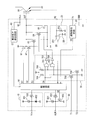
- FIG. 2 is a circuit diagram showing a configuration of the first embodiment of the control device of the present invention.
- the control device according to the first embodiment is applied to the IPM control devices 1 to 6 shown in FIG.
- This control device corresponds to, for example, the control device 6 shown in FIG. 1, and drives and controls the switching element Q6 connected to the output terminal OUT as shown in FIG. Therefore, as shown in FIG. 2, the control device includes an input signal receiving circuit 10, an overcurrent detection circuit 20, an overheat detection circuit 30, a potential drop detection circuit 40, a drive circuit 50, and a plurality of transistors 61.
- a transistor operation control unit 70 To 65, a transistor operation control unit 70, and an alarm output circuit 80.
- the control device also includes a power supply voltage terminal Vcc, a reference potential terminal GND, an input terminal Vin, an output terminal OUT, an overcurrent detection terminal OC, an overheat detection terminal TE, an alarm terminal ALM, and test terminals T1 and T2. .
- Each of the plurality of transistors 61 to 65 has the following function according to the drive control of the switching element Q6, and has a withstand voltage of 20 [V] or more.
- the output terminals of the plurality of transistors 61 to 65 are commonly connected to the output terminal OUT.
- the transistor 61 functions as a turn-on transistor that is used when the switching element Q6 connected to the output terminal OUT is turned on during normal switching.
- the transistor 61 is a P-type MOS transistor, and its output current is, for example, 1.5 [A].
- the transistor 62 functions as a soft cutoff transistor that is used to gradually turn off the switching element Q6 when the overcurrent detection circuit 20 detects an overcurrent.
- the transistor 62 is an N-type MOS transistor, and its output current is, for example, 200 [mA].
- the transistor 63 is an off-protection transistor used for lowering the output impedance in order to prevent a malfunction when the switching element Q6 is normally switched on.
- the transistor 63 is an N-type MOS transistor, and its output current is, for example, 1 [A].
- Each of the transistors 64 and 65 has the same function as a turn-off transistor used when the switching element Q6 is turned off during normal switching. This turn-off transistor is divided into a plurality of transistors 64 and 65.
- Each of the output currents of the transistors 64 and 65 is, for example, 1.5 [A]. Therefore, the two transistors 64 and 65 function as a total output current of 3 [A].
- the turn-off transistor may be divided into a plurality of transistors having an ability smaller than the ability (output current) in the case of being constituted by a single transistor.
- the input signal receiving circuit 10 receives an input signal supplied to the input terminal Vin and outputs a signal corresponding to the reception to the driving circuit 50. Therefore, the input signal receiving circuit 10 includes a current source 101, a Zener diode 102, and an inverter 103 with a hysteresis function.
- the overcurrent detection circuit 20 detects whether or not the current flowing through a switching element (not shown) connected to the output terminal OUT is an overcurrent. If an overcurrent is detected, the overcurrent detection signal S5 is used as a drive circuit. Output to 50. For this reason, the overcurrent detection circuit 20 includes a comparator 201 and a resistor 202. A part of the current flowing through the switching element is input to the overcurrent detection terminal OC, and a detection voltage is generated at both ends of the resistor 201 by this input current. The comparator 201 compares the detected voltage with the reference voltage ER, and outputs an overcurrent detection signal S5 to the drive circuit 50 when the detected voltage is equal to or higher than the reference voltage ER.
- the overheat detection circuit 30 detects whether or not a switching element (not shown) connected to the output terminal OUT is in an overheat state, and outputs an overheat detection signal S6 to the drive circuit 50 when the overheat state is detected. To do. For this reason, the overheat detection circuit 30 inputs a detection current of a temperature sensor (not shown) that detects a part of the current flowing through the switching element to the overheat detection terminal TE. Then, based on the detected current, it is determined whether or not the switching element is in an overheated state. If it is determined that the switching element is in an overheated state, an overheat detection signal S6 is output to the drive circuit 50.
- the potential drop detection circuit 40 detects the power supply voltage supplied to the power supply voltage terminal Vcc, and outputs a potential drop signal S7 to the drive circuit 50 when the detected voltage is not more than a predetermined value.
- the drive circuit 50 outputs a drive signal S1 for turning on the switching element Q6 and a drive signal S4 for turning off the switching element Q6 based on the input signal received by the input signal receiving circuit 10. Therefore, when the switching element Q6 is turned on, only the transistor 61 is turned on by the drive signal S1, the power supply voltage Vcc is applied to the gate of the switching element Q6, and the gate is charged. Further, when the switching element Q6 is turned off, only the turn-off transistors 64 and 65 are turned on all at once by the drive signal S4, the gate of the switching element Q6 is connected to the ground, and the gate charge is discharged.
- the drive circuit 50 drives the switching element Q6 gently based on the overcurrent detection signal S5 output from the overcurrent detection circuit 20 or the overheat detection signal S6 output from the overheat detection circuit 30. S2 is output. Therefore, the drive signal S2 turns on the soft cutoff transistor 62, connects the gate of the switching element Q6 to the ground, and gradually discharges the gate charge.
- the drive circuit 50 outputs the drive signal S3 when turning off for protection of the switching element Q6 based on the potential drop signal S7 output from the potential drop detection circuit 40.
- the drive signal S3 turns on the off-protection transistor 63, connects the gate of the switching element Q6 to the ground, and protects the switching element Q6.
- the drive circuit 50 outputs an overcurrent detection signal S5 from the overcurrent detection circuit 20, outputs an overheat detection signal S6 from the overheat detection circuit 30, or receives a potential drop detection signal S7 from the potential drop detection circuit 40.
- the alarm signal S8 is output to the alarm output circuit 80. Further, when the alarm factor is eliminated, the output of the alarm signal S8 is stopped.
- the alarm output circuit 80 outputs the alarm signal S8 to the alarm terminal ALM when the drive circuit 50 outputs the alarm signal S8, and stops the output of the alarm signal S8 when the cause of the alarm is resolved. Therefore, the alarm output circuit 80 includes a current source 801, a transistor 802, and an inverter 803 with a hysteresis function.
- the transistor operation control unit 70 operates the two transistors 64 and 65 having the same function in the normal operation so as to realize the original function, and operates the two transistors 64 and 65 individually in the test operation.
- the output current can be measured with an IC tester.
- the transistor operation control unit 70 controls the two transistors 64 and 65 on or off simultaneously or collectively with the same drive signal S4 output from the drive circuit 50.
- the transistor operation control unit 70 includes NAND circuits (NAND circuits) 701 and 702, an inverter circuit 703, pull-up resistors 705 and 706, and transistors 708 and 709.
- a drive signal S4 output from the drive circuit 50 is input to one of the input terminals of the NAND circuits 701 and 702.
- a power supply voltage is applied to the other input terminal of the NAND circuit 701 through a pull-up resistor 706.
- the other input terminal of the NAND circuit 701 is connected to the ground via the transistor 709.
- a power supply voltage is applied to the other input terminal of the NAND circuit 702 via a pull-up resistor 705.
- the other input terminal of the NAND circuit 702 is connected to the ground via the transistor 708.
- the output terminal of the NAND circuit 701 is connected to the gate of the transistor 64 via the inverter circuit 703.
- the output terminal of the NAND circuit 702 is connected to the gate of the transistor 65 via the inverter circuit 704.
- the NAND circuit 701 and the inverter circuit 703 function as an AND circuit.
- the NAND circuit 702 and the inverter circuit 704 function as an AND circuit.
- Inverter circuits 703 and 704 each function as a buffer circuit.
- the control device having such a configuration is manufactured by a semiconductor wafer process, and a shipping test (operation test) of the control device is performed by probing in the state of a silicon wafer. In the shipping test of this control device, an IC tester is used, and the output current is measured for each of the transistors 61 to 65 in the output stage.
- this control device includes a transistor operation control unit 70.
- the transistor operation control unit 70 has a normal operation and a test operation. The operation in each case will be described.
- a test operation when an H level (high level) signal is applied only to the test terminal T1, the transistor 708 is turned on, so that one input terminal of the NAND circuit 702 becomes L level (low level). .
- the drive signal S4 output from the drive circuit 50 is supplied to the gate of the transistor 64 via the NAND circuit 701 and the inverter 703. Therefore, when the transistor 64 is turned on by the drive signal S4, the output current of the transistor 64 can be measured by the IC tester.
- the transistor 709 is turned on, so that one input terminal of the NAND circuit 701 becomes L level.
- the transistor 708 is off, one input terminal of the NAND circuit 702 becomes H level. Therefore, the drive signal S4 output from the drive circuit 50 is supplied to the gate of the transistor 65 via the NAND circuit 702 and the inverter 704. Therefore, when the transistor 65 is turned on by the drive signal S4, the output current of the transistor 65 can be measured by the IC tester.
- both transistors 708 and 709 are not operated. For this reason, the power supply voltage is applied to one of the input terminals of each of the NAND circuits 701 and 702 via the pull-up resistors 705 and 706, so that one of the input terminals of each of the NAND circuits 701 and 702 is at the H level. Become. Therefore, the drive signal S4 output from the drive circuit 50 is supplied to the gate of the transistor 64 via the NAND circuit 701 and the inverter 703, and is supplied to the gate of the transistor 65 via the NAND circuit 702 and the inverter 704. Is done. Therefore, the transistors 64 and 65 are collectively driven by the same drive signal S4.
- the turn-off transistor for turning off the switching element is divided into two transistors 64 and 65.
- the transistor operation control unit 70 is provided in addition to the configuration. For this reason, according to the first embodiment, during the test operation of the shipping test, the two transistors 64 and 65 are individually operated to use the respective output currents without using the existing IC tester without improving the evaluation board. And can be measured with high accuracy. In the normal operation after shipment, the two transistors 64 and 65 having the same function can perform an operation for realizing the original function.
- FIG. 3 is a circuit diagram showing a configuration of the second embodiment of the control device of the present invention.
- the control device according to the second embodiment is applied to the IPM control devices 1 to 6 shown in FIG.
- This control device corresponds to, for example, the control device 6 shown in FIG. 1, and drives and controls the switching element Q6 connected to the output terminal OUT as shown in FIG.
- the control device includes an input signal receiving circuit 10A, an overcurrent detection circuit 20A, an overheat detection circuit 30, a potential drop detection circuit 40, a drive circuit 50A, and a plurality of transistors 61.
- a transistor operation control unit 70A To 63 and 66 to 68, a transistor operation control unit 70A, an alarm output circuit 80A, and a regulator 90.
- this control device includes a power supply voltage terminal Vcc, a reference potential terminal GND, an input terminal Vin, an output terminal OUT, an overcurrent detection terminal OC, an overheat detection terminal TE, an alarm terminal ALM, a data input terminal DATE, and a clock input terminal CLK. It has.
- a power supply voltage of about 15 [V] is applied to the power supply voltage terminal Vcc, and the plurality of transistors 61 to 63 and 66 to 68 are operated by this power supply voltage.
- the regulator 90 generates a voltage of 5 [V] stabilized by the power supply voltage, and each circuit and each unit operate by the generated voltage.
- Each of the plurality of transistors 61 to 63 and 66 to 68 has the following function according to the drive control of the switching element Q6, and has a withstand voltage of 20 [V] or more.
- the output terminals of the plurality of transistors 61 to 63 and 66 to 68 are commonly connected to the output terminal OUT.
- the transistors 61 to 63 have the same functions as the transistors 61 to 63 in FIG. However, in this example, the output current of the turn-on transistor 61 is 1 [A].
- the output current of the soft cutoff transistor 62 is 400 [mA].
- Each of the transistors 66 to 68 has the same function as a turn-off transistor used for turning off the normal switching of the switching element Q6.
- the turn-off transistor is divided into a plurality of transistors 66 to 68, and each of the output currents of the transistors 66 to 68 is, for example, 1 [A]. Therefore, the three transistors 66 to 68 function as a total output current of 3 [A].
- the input signal receiving circuit 10A receives an input signal supplied to the input terminal Vin, and outputs a signal corresponding to the reception to the drive circuit 50A.
- the input signal receiving circuit 10 includes a current source 101, resistors 104 and 105, a Zener diode 102, and an inverter 103 with a hysteresis function.
- the overcurrent detection circuit 20A detects whether or not the current flowing through the switching element Q6 connected to the output terminal OUT is an overcurrent. If an overcurrent is detected, the overcurrent detection circuit 20A outputs an overcurrent detection signal S5 to the drive circuit 50A. .
- the overcurrent detection circuit 20A includes a comparator 201 and voltage dividing resistors 203 and 204. A part of the current flowing through the switching element Q6 is input to the overcurrent detection terminal OC, and a divided voltage is generated by the voltage dividing resistors 203 and 204 by this input current.
- the comparator 201 compares the divided voltage with the reference voltage ER, and outputs an overcurrent detection signal S5 to the drive circuit 50A when the divided voltage is equal to or higher than the reference voltage ER.
- the overheat detection circuit 30 is configured in the same manner as the overheat detection circuit 30 of FIG. 2, and outputs an overheat detection signal S6 to the drive circuit 50A.
- the potential drop detection circuit 40 is configured in the same manner as the potential drop detection circuit 40 of FIG. 2, and outputs a potential drop signal S7 to the drive circuit 50A.
- the drive circuit 50A outputs a drive signal S1 for turning on the switching element Q6 and a drive signal S4 for turning off the switching element Q6 based on the input signal received by the input signal receiving circuit 10A. Therefore, when the switching element Q6 is turned on, only the transistor 61 is turned on by the drive signal S1, the power supply voltage Vcc is applied to the gate of the switching element Q6, and the gate is charged. When the switching element Q6 is turned off, only the turn-off transistors 66 to 68 are turned on at the same time by the drive signal S4, the gate of the switching element Q6 is connected to the ground, and the gate charge is discharged.
- the drive circuit 50A drives the switching element Q6 gently based on the overcurrent detection signal S5 output from the overcurrent detection circuit 20A or the overheat detection signal S6 output from the overheat detection circuit 30. S2 is output. Therefore, the drive signal S2 turns on the soft cutoff transistor 62, connects the gate of the switching element Q6 to the ground, and gradually discharges the gate charge.
- the drive circuit 50A outputs a drive signal S3 when turning off for protection of the switching element Q6 based on the potential drop signal S7 output from the potential drop detection circuit 40.
- the drive signal S3 turns on the off-protection transistor 63, connects the gate of the switching element Q6 to the ground, and protects the switching element Q6.
- the drive circuit 50A receives the overcurrent detection signal S5 from the overcurrent detection circuit 20A, the overheat detection signal S6 from the overheat detection circuit 30, or the potential drop detection signal S7 from the potential drop detection circuit 40.
- the alarm signal S8 is output to the alarm output circuit 80A. Further, when the alarm factor is eliminated, the output of the alarm signal S8 is stopped.
- the alarm output circuit 80A outputs the alarm signal S8 to the alarm terminal ALM when the drive circuit 50A outputs the alarm signal S8, and stops the output of the alarm signal S8 when the cause of the alarm is resolved. Therefore, the alarm output circuit 80A includes a current source 801, a transistor 802, resistors 804 and 805, a Zener diode 806, and an inverter 803 with a hysteresis function.
- the transistor operation control unit 70A operates the three transistors 66 to 68 having the same function in the normal operation so as to realize the original function, and operates the three transistors 66 to 68 individually in the test operation.
- the output current can be measured with an IC tester.
- the transistor operation control unit 70A controls the three transistors 66 to 68 simultaneously or collectively with the same drive signal S4 output from the drive circuit 50A.
- the transistor operation control unit 70A includes NAND circuits 711 to 713, inverter circuits 714 to 716, pull-up resistors 717 to 719, transistors 720 to 722, and a shift register 730. ing.
- a drive signal S4 output from the drive circuit 50A is input to each of one input terminals of the NAND circuits 711 to 713.
- a power supply voltage is applied to each of the other input terminals of the NAND circuits 711 to 713 via the pull-up resistors 717 to 719.
- the other input terminals of the NAND circuits 711 to 713 are connected to the ground via the transistors 720 to 722, respectively.
- the outputs of the output terminals 740, 750, and 760 of the shift register 730 are input to the gates of the transistors 720 to 722, respectively.
- the shift register 730 sequentially inputs input data with a clock, and outputs the input data in parallel from output terminals 740, 750, and 760. Therefore, the shift register 730 is connected to a data input terminal DATA to which data is input and a clock input terminal CLK to which a clock is input.
- the control device having such a configuration is manufactured by a semiconductor wafer process, and a shipping test (operation test) of the control device is performed by probing in the state of a silicon wafer. An IC tester is used in the shipping test of this control device, and the output current is measured for each of the transistors 61 to 63 and 66 to 68 in the output stage.
- the turn-off transistors 66 to 68 are constituted by one, and when the output current is 3 [A], the above IC tester is used. With this, the output current cannot be measured.
- the turn-off transistor is divided into a plurality of transistors 66 to 68, and each of the output currents of the transistors 66 to 68 is, for example, 1 [A]. Further, this control device includes a transistor operation control unit 70A.
- the transistor operation control unit 70A has a normal operation and a test operation, and the operation in each case will be described.
- the shift register 730 is operated with a clock, test data is sequentially input, and the input data is output from the output terminals 740, 750, and 760, and the gates of the transistors 720 to 722 are input. To supply.
- the transistor 720 When the output terminals 740, 750, and 760 of the shift register 730 are “L”, “H”, and “H”, the transistor 720 is turned off, the transistor 721 is turned on, and the transistor 722 is turned on. .
- the drive signal S4 output from the drive circuit 50A can be supplied to the gate of the transistor 66 via the NAND circuit 711 and the inverter 714. Therefore, when the transistor 66 is turned on by the drive signal S4, the output current of the transistor 66 can be measured by the IC tester.
- the transistor 720 is on, the transistor 721 is off, and the transistor 722 is on Become.
- the drive signal S4 output from the drive circuit 50A can be supplied to the gate of the transistor 67 via the NAND circuit 712 and the inverter 715. Therefore, when the transistor 67 is turned on by the drive signal S4, the output current of the transistor 67 can be measured by the IC tester.
- the transistor 720 is on, the transistor 721 is on, and the transistor 722 is off It becomes.
- the drive signal S4 output from the drive circuit 50A can be supplied to the gate of the transistor 68 via the NAND circuit 713 and the inverter 716. Therefore, when the transistor 68 is turned on by the drive signal S4, the output current of the transistor 68 can be measured by the IC tester.
- the transistors 720 to 722 and the shift register 730 are not operated. Therefore, since the power supply voltage is applied to each of the input terminals of the NAND circuits 711 to 713 via the pull-up resistors 717 to 719, all of the input terminals of the NAND circuits 711 to 713 are at the H level. Clearly, the drive signal S4 output from the drive circuit 50A is supplied to the gate of the transistor 66 via the NAND circuit 711 and the inverter 714, and is supplied to the gate of the transistor 67 via the NAND circuit 712 and the inverter 715. In addition, the signal is supplied to the gate of the transistor 68 via the NAND circuit 713 and the inverter 716. For this reason, the transistors 66 to 68 are collectively driven by the same drive signal S4.
- the turn-off transistor for turning off the switching element is constituted by the three transistors 66-68.
- the transistor operation control unit 70A is provided in addition to the configuration. Therefore, according to the second embodiment, during the test operation of the shipping test, the three transistors 66 to 68 are individually operated to use the output currents and the existing IC tester without improving the evaluation board. And can be measured with high accuracy. In the normal operation after shipment, the three transistors 66 to 68 having the same function can perform an operation for realizing the original function.
- the transistor for turning off the switching element is composed of the plurality of transistors 64 and 65, and the transistor operation control unit 70 is provided accordingly.
- the transistor such as the transistor 61 for turning on the switching element and the transistor 63 for protecting the switching element may be composed of a plurality of transistors.
- a transistor operation control unit similar to the transistor operation control unit 70 is provided between the drive circuit 50 and the plurality of transistors.
- the transistor for turning off the switching element is composed of the plurality of transistors 66 to 68, and the transistor operation control unit 70A is provided in accordance with this.
- the transistor such as the transistor 61 for turning on the switching element and the transistor 63 for protecting the switching element may be composed of a plurality of transistors.
- a transistor operation control unit similar to the transistor operation control unit 70A is provided between the drive circuit 50A and the plurality of transistors.
- the case of the IGBT is described as an example of the switching element.
- the present invention can also be applied to drive control of a power transistor or the like.
- the present invention is applied to a control device for a switching element of a voltage source inverter that drives a motor, for example.
Landscapes
- Physics & Mathematics (AREA)
- General Physics & Mathematics (AREA)
- Electronic Switches (AREA)
- Testing Of Individual Semiconductor Devices (AREA)
- Tests Of Electronic Circuits (AREA)
- Power Conversion In General (AREA)
Abstract
La présente invention concerne un dispositif capable de mesurer précisément le courant de sortie d'un transistor servant à piloter et à commander un élément de commutation, en utilisant un testeur de CI existant et sans améliorer une carte d'évaluation. Selon un mode de réalisation, la présente invention comporte un circuit (50) de pilotage, une pluralité de transistors (61-65) servant à piloter et à commander un élément (Q6) de commutation, et une unité (70) de commande du fonctionnement des transistors. Une partie de la pluralité de transistors (64, 65) sert à mettre l'élément de commutation (Q6) à l'état bloqué. En fonctionnement normal, l'unité (70) de commande du fonctionnement des transistors commande l'état passant / bloqué des deux transistors (64, 65) simultanément ou en bloc, en utilisant le même signal (S4) de pilotage émanant du circuit (50) de pilotage. En fonctionnement de test, un des transistors (64, 65) est sélectionné dans l'ordre, le même signal (S4) de pilotage est fourni au transistor sélectionné et les transistors (64, 65) sont pilotés individuellement.
Priority Applications (2)
| Application Number | Priority Date | Filing Date | Title |
|---|---|---|---|
| JP2013513907A JP5397571B2 (ja) | 2011-05-11 | 2012-04-06 | 制御装置 |
| US13/715,298 US9473133B2 (en) | 2011-05-11 | 2012-12-14 | Control device |
Applications Claiming Priority (2)
| Application Number | Priority Date | Filing Date | Title |
|---|---|---|---|
| JP2011106181 | 2011-05-11 | ||
| JP2011-106181 | 2011-05-11 |
Related Child Applications (1)
| Application Number | Title | Priority Date | Filing Date |
|---|---|---|---|
| US13/715,298 Continuation US9473133B2 (en) | 2011-05-11 | 2012-12-14 | Control device |
Publications (1)
| Publication Number | Publication Date |
|---|---|
| WO2012153458A1 true WO2012153458A1 (fr) | 2012-11-15 |
Family
ID=47138951
Family Applications (1)
| Application Number | Title | Priority Date | Filing Date |
|---|---|---|---|
| PCT/JP2012/002424 Ceased WO2012153458A1 (fr) | 2011-05-11 | 2012-04-06 | Dispositif de commande |
Country Status (3)
| Country | Link |
|---|---|
| US (1) | US9473133B2 (fr) |
| JP (1) | JP5397571B2 (fr) |
| WO (1) | WO2012153458A1 (fr) |
Cited By (3)
| Publication number | Priority date | Publication date | Assignee | Title |
|---|---|---|---|---|
| CN104880262A (zh) * | 2014-02-28 | 2015-09-02 | 鸿富锦精密工业(武汉)有限公司 | 电源过热指示系统 |
| KR101836247B1 (ko) * | 2012-12-12 | 2018-03-08 | 현대자동차 주식회사 | 인버터 구동 장치 |
| JP2021506183A (ja) * | 2018-03-08 | 2021-02-18 | ジン−ジン エレクトリック テクノロジーズ カンパニー リミテッド | モータコントローラのigbt駆動回路及びモータコントローラ |
Families Citing this family (10)
| Publication number | Priority date | Publication date | Assignee | Title |
|---|---|---|---|---|
| JP5720641B2 (ja) * | 2012-08-21 | 2015-05-20 | 株式会社デンソー | スイッチングモジュール |
| JP6286899B2 (ja) * | 2013-07-03 | 2018-03-07 | 富士電機株式会社 | 絶縁ゲート型半導体素子の駆動装置および電力変換装置 |
| JP5880494B2 (ja) * | 2013-07-04 | 2016-03-09 | 株式会社デンソー | スイッチング制御回路 |
| JP6256292B2 (ja) * | 2014-10-22 | 2018-01-10 | 株式会社デンソー | 温度保護装置 |
| JP7087471B2 (ja) * | 2018-03-08 | 2022-06-21 | オムロン株式会社 | 電力変換装置及びインバータの制御方法 |
| CN111684722B (zh) * | 2018-08-09 | 2023-10-20 | 富士电机株式会社 | 半导体装置 |
| JP7038647B2 (ja) * | 2018-12-12 | 2022-03-18 | 三菱電機株式会社 | インテリジェントパワーモジュール |
| FR3093815B1 (fr) | 2019-03-11 | 2021-02-26 | Crouzet Automatismes | Installation electrique comportant un module de surveillance |
| FR3093814B1 (fr) * | 2019-03-11 | 2021-02-26 | Crouzet Automatismes | Installation electrique comportant un module de surveillance |
| JP7767750B2 (ja) * | 2021-06-30 | 2025-11-12 | 富士電機株式会社 | 集積回路、及びパワーモジュール |
Citations (2)
| Publication number | Priority date | Publication date | Assignee | Title |
|---|---|---|---|---|
| JPH08274614A (ja) * | 1995-03-30 | 1996-10-18 | Nec Corp | 半導体集積回路およびその試験方法 |
| JP2010075007A (ja) * | 2008-09-22 | 2010-04-02 | Denso Corp | 電力変換回路の駆動回路 |
Family Cites Families (11)
| Publication number | Priority date | Publication date | Assignee | Title |
|---|---|---|---|---|
| DE19825258B4 (de) * | 1998-06-05 | 2005-11-17 | Telefonaktiebolaget Lm Ericsson (Publ) | Ausgangspufferschaltkreis zum Übertragen von digitalen Signalen über eine Übertragungsleitung mit Preemphasis |
| JP2001128464A (ja) * | 1999-10-26 | 2001-05-11 | Fuji Electric Co Ltd | 電力変換装置 |
| US6255867B1 (en) * | 2000-02-23 | 2001-07-03 | Pericom Semiconductor Corp. | CMOS output buffer with feedback control on sources of pre-driver stage |
| EP1358709A2 (fr) * | 2001-02-06 | 2003-11-05 | Harman International Industries, Inc. | Circuit de commande de grille en demi-pont |
| US7061301B2 (en) * | 2003-12-19 | 2006-06-13 | Power Integrations, Inc. | Method and apparatus switching a semiconductor switch with a multi-state drive circuit |
| JP4432825B2 (ja) * | 2005-04-22 | 2010-03-17 | 株式会社デンソー | 内燃機関用点火装置 |
| JP2008216169A (ja) * | 2007-03-07 | 2008-09-18 | Matsushita Electric Ind Co Ltd | 半導体装置 |
| JP2008271389A (ja) * | 2007-04-24 | 2008-11-06 | Matsushita Electric Ind Co Ltd | 出力回路及び多出力回路 |
| KR100884603B1 (ko) * | 2007-05-09 | 2009-02-19 | 주식회사 하이닉스반도체 | 반도체소자의 버퍼장치 |
| JP5401774B2 (ja) | 2007-08-27 | 2014-01-29 | 富士電機株式会社 | 半導体素子のゲート駆動回路 |
| US7884583B2 (en) * | 2008-06-30 | 2011-02-08 | Infineon Technologies Austria Ag | Speed recognition for half bridge control |
-
2012
- 2012-04-06 WO PCT/JP2012/002424 patent/WO2012153458A1/fr not_active Ceased
- 2012-04-06 JP JP2013513907A patent/JP5397571B2/ja active Active
- 2012-12-14 US US13/715,298 patent/US9473133B2/en active Active
Patent Citations (2)
| Publication number | Priority date | Publication date | Assignee | Title |
|---|---|---|---|---|
| JPH08274614A (ja) * | 1995-03-30 | 1996-10-18 | Nec Corp | 半導体集積回路およびその試験方法 |
| JP2010075007A (ja) * | 2008-09-22 | 2010-04-02 | Denso Corp | 電力変換回路の駆動回路 |
Cited By (5)
| Publication number | Priority date | Publication date | Assignee | Title |
|---|---|---|---|---|
| KR101836247B1 (ko) * | 2012-12-12 | 2018-03-08 | 현대자동차 주식회사 | 인버터 구동 장치 |
| CN104880262A (zh) * | 2014-02-28 | 2015-09-02 | 鸿富锦精密工业(武汉)有限公司 | 电源过热指示系统 |
| JP2021506183A (ja) * | 2018-03-08 | 2021-02-18 | ジン−ジン エレクトリック テクノロジーズ カンパニー リミテッド | モータコントローラのigbt駆動回路及びモータコントローラ |
| US11323112B2 (en) | 2018-03-08 | 2022-05-03 | Jing-Jin Electric Technologies Co., Ltd | IGBT drive circuit for motor controller, and motor controller |
| JP7072066B2 (ja) | 2018-03-08 | 2022-05-19 | ジン-ジン エレクトリック テクノロジーズ カンパニー リミテッド | モータコントローラのigbt駆動回路及びモータコントローラ |
Also Published As
| Publication number | Publication date |
|---|---|
| JP5397571B2 (ja) | 2014-01-22 |
| US20130106470A1 (en) | 2013-05-02 |
| JPWO2012153458A1 (ja) | 2014-07-31 |
| US9473133B2 (en) | 2016-10-18 |
Similar Documents
| Publication | Publication Date | Title |
|---|---|---|
| JP5397571B2 (ja) | 制御装置 | |
| US10374593B2 (en) | Semiconductor device | |
| US11431162B2 (en) | Smart electronic switch | |
| US9698654B2 (en) | Soft shutdown for isolated drivers | |
| US9019677B2 (en) | Semiconductor switching element drive circuit | |
| JP5315026B2 (ja) | 半導体装置 | |
| TWI568179B (zh) | 高壓閘極驅動電路 | |
| JP4619812B2 (ja) | ゲート駆動回路 | |
| US20140218097A1 (en) | System and method for a driver circuit | |
| JP7443679B2 (ja) | 半導体装置 | |
| US20140036401A1 (en) | Semiconductor device, electronic device, and method of testing the semiconductor device | |
| CN101189795A (zh) | 电源控制器和半导体装置 | |
| US11955957B2 (en) | Smart electronic switch | |
| US7696650B2 (en) | Driving circuit for switching elements | |
| WO2017208668A1 (fr) | Dispositif d'excitation d'élément semi-conducteur | |
| CN108337922A (zh) | 半导体器件驱动电路及逆变器装置 | |
| JP2023055784A (ja) | 半導体装置及び半導体装置の識別方法 | |
| WO2014203678A1 (fr) | Module semi-conducteur | |
| US10116310B2 (en) | Level shift circuit, integrated circuit, and power semiconductor module | |
| US11984879B2 (en) | Drive circuit | |
| CN113960462B (zh) | 开关应用的过电流感测方案 | |
| US11929666B2 (en) | Gate drive circuit and power conversion device | |
| JP4712024B2 (ja) | 半導体電力変換装置の過電流保護装置 | |
| US12191844B2 (en) | Overcurrent detection circuit, drive control device, and power conversion device | |
| JP2009089152A (ja) | ドライバ装置 |
Legal Events
| Date | Code | Title | Description |
|---|---|---|---|
| 121 | Ep: the epo has been informed by wipo that ep was designated in this application |
Ref document number: 12782229 Country of ref document: EP Kind code of ref document: A1 |
|
| ENP | Entry into the national phase |
Ref document number: 2013513907 Country of ref document: JP Kind code of ref document: A |
|
| NENP | Non-entry into the national phase |
Ref country code: DE |
|
| 122 | Ep: pct application non-entry in european phase |
Ref document number: 12782229 Country of ref document: EP Kind code of ref document: A1 |