WO2012153468A1 - 電気光学装置の制御装置、電気光学装置の制御方法、電気光学装置及び電子機器 - Google Patents
電気光学装置の制御装置、電気光学装置の制御方法、電気光学装置及び電子機器 Download PDFInfo
- Publication number
- WO2012153468A1 WO2012153468A1 PCT/JP2012/002670 JP2012002670W WO2012153468A1 WO 2012153468 A1 WO2012153468 A1 WO 2012153468A1 JP 2012002670 W JP2012002670 W JP 2012002670W WO 2012153468 A1 WO2012153468 A1 WO 2012153468A1
- Authority
- WO
- WIPO (PCT)
- Prior art keywords
- pixel
- voltage
- gradation
- value
- storage area
- Prior art date
- Legal status (The legal status is an assumption and is not a legal conclusion. Google has not performed a legal analysis and makes no representation as to the accuracy of the status listed.)
- Ceased
Links
Images










Classifications
-
- G—PHYSICS
- G09—EDUCATION; CRYPTOGRAPHY; DISPLAY; ADVERTISING; SEALS
- G09G—ARRANGEMENTS OR CIRCUITS FOR CONTROL OF INDICATING DEVICES USING STATIC MEANS TO PRESENT VARIABLE INFORMATION
- G09G3/00—Control arrangements or circuits, of interest only in connection with visual indicators other than cathode-ray tubes
- G09G3/20—Control arrangements or circuits, of interest only in connection with visual indicators other than cathode-ray tubes for presentation of an assembly of a number of characters, e.g. a page, by composing the assembly by combination of individual elements arranged in a matrix no fixed position being assigned to or needed to be assigned to the individual characters or partial characters
- G09G3/34—Control arrangements or circuits, of interest only in connection with visual indicators other than cathode-ray tubes for presentation of an assembly of a number of characters, e.g. a page, by composing the assembly by combination of individual elements arranged in a matrix no fixed position being assigned to or needed to be assigned to the individual characters or partial characters by control of light from an independent source
- G09G3/3433—Control arrangements or circuits, of interest only in connection with visual indicators other than cathode-ray tubes for presentation of an assembly of a number of characters, e.g. a page, by composing the assembly by combination of individual elements arranged in a matrix no fixed position being assigned to or needed to be assigned to the individual characters or partial characters by control of light from an independent source using light modulating elements actuated by an electric field and being other than liquid crystal devices and electrochromic devices
- G09G3/344—Control arrangements or circuits, of interest only in connection with visual indicators other than cathode-ray tubes for presentation of an assembly of a number of characters, e.g. a page, by composing the assembly by combination of individual elements arranged in a matrix no fixed position being assigned to or needed to be assigned to the individual characters or partial characters by control of light from an independent source using light modulating elements actuated by an electric field and being other than liquid crystal devices and electrochromic devices based on particles moving in a fluid or in a gas, e.g. electrophoretic devices
-
- G—PHYSICS
- G02—OPTICS
- G02F—OPTICAL DEVICES OR ARRANGEMENTS FOR THE CONTROL OF LIGHT BY MODIFICATION OF THE OPTICAL PROPERTIES OF THE MEDIA OF THE ELEMENTS INVOLVED THEREIN; NON-LINEAR OPTICS; FREQUENCY-CHANGING OF LIGHT; OPTICAL LOGIC ELEMENTS; OPTICAL ANALOGUE/DIGITAL CONVERTERS
- G02F1/00—Devices or arrangements for the control of the intensity, colour, phase, polarisation or direction of light arriving from an independent light source, e.g. switching, gating or modulating; Non-linear optics
- G02F1/01—Devices or arrangements for the control of the intensity, colour, phase, polarisation or direction of light arriving from an independent light source, e.g. switching, gating or modulating; Non-linear optics for the control of the intensity, phase, polarisation or colour
- G02F1/165—Devices or arrangements for the control of the intensity, colour, phase, polarisation or direction of light arriving from an independent light source, e.g. switching, gating or modulating; Non-linear optics for the control of the intensity, phase, polarisation or colour based on translational movement of particles in a fluid under the influence of an applied field
- G02F1/166—Devices or arrangements for the control of the intensity, colour, phase, polarisation or direction of light arriving from an independent light source, e.g. switching, gating or modulating; Non-linear optics for the control of the intensity, phase, polarisation or colour based on translational movement of particles in a fluid under the influence of an applied field characterised by the electro-optical or magneto-optical effect
- G02F1/167—Devices or arrangements for the control of the intensity, colour, phase, polarisation or direction of light arriving from an independent light source, e.g. switching, gating or modulating; Non-linear optics for the control of the intensity, phase, polarisation or colour based on translational movement of particles in a fluid under the influence of an applied field characterised by the electro-optical or magneto-optical effect by electrophoresis
-
- G—PHYSICS
- G09—EDUCATION; CRYPTOGRAPHY; DISPLAY; ADVERTISING; SEALS
- G09G—ARRANGEMENTS OR CIRCUITS FOR CONTROL OF INDICATING DEVICES USING STATIC MEANS TO PRESENT VARIABLE INFORMATION
- G09G3/00—Control arrangements or circuits, of interest only in connection with visual indicators other than cathode-ray tubes
- G09G3/20—Control arrangements or circuits, of interest only in connection with visual indicators other than cathode-ray tubes for presentation of an assembly of a number of characters, e.g. a page, by composing the assembly by combination of individual elements arranged in a matrix no fixed position being assigned to or needed to be assigned to the individual characters or partial characters
- G09G3/2007—Display of intermediate tones
-
- G—PHYSICS
- G09—EDUCATION; CRYPTOGRAPHY; DISPLAY; ADVERTISING; SEALS
- G09G—ARRANGEMENTS OR CIRCUITS FOR CONTROL OF INDICATING DEVICES USING STATIC MEANS TO PRESENT VARIABLE INFORMATION
- G09G3/00—Control arrangements or circuits, of interest only in connection with visual indicators other than cathode-ray tubes
- G09G3/20—Control arrangements or circuits, of interest only in connection with visual indicators other than cathode-ray tubes for presentation of an assembly of a number of characters, e.g. a page, by composing the assembly by combination of individual elements arranged in a matrix no fixed position being assigned to or needed to be assigned to the individual characters or partial characters
- G09G3/2092—Details of a display terminals using a flat panel, the details relating to the control arrangement of the display terminal and to the interfaces thereto
-
- G—PHYSICS
- G09—EDUCATION; CRYPTOGRAPHY; DISPLAY; ADVERTISING; SEALS
- G09G—ARRANGEMENTS OR CIRCUITS FOR CONTROL OF INDICATING DEVICES USING STATIC MEANS TO PRESENT VARIABLE INFORMATION
- G09G2320/00—Control of display operating conditions
- G09G2320/02—Improving the quality of display appearance
- G09G2320/0204—Compensation of DC component across the pixels in flat panels
-
- G—PHYSICS
- G09—EDUCATION; CRYPTOGRAPHY; DISPLAY; ADVERTISING; SEALS
- G09G—ARRANGEMENTS OR CIRCUITS FOR CONTROL OF INDICATING DEVICES USING STATIC MEANS TO PRESENT VARIABLE INFORMATION
- G09G2320/00—Control of display operating conditions
- G09G2320/02—Improving the quality of display appearance
- G09G2320/0252—Improving the response speed
-
- G—PHYSICS
- G09—EDUCATION; CRYPTOGRAPHY; DISPLAY; ADVERTISING; SEALS
- G09G—ARRANGEMENTS OR CIRCUITS FOR CONTROL OF INDICATING DEVICES USING STATIC MEANS TO PRESENT VARIABLE INFORMATION
- G09G2340/00—Aspects of display data processing
- G09G2340/16—Determination of a pixel data signal depending on the signal applied in the previous frame
-
- G—PHYSICS
- G09—EDUCATION; CRYPTOGRAPHY; DISPLAY; ADVERTISING; SEALS
- G09G—ARRANGEMENTS OR CIRCUITS FOR CONTROL OF INDICATING DEVICES USING STATIC MEANS TO PRESENT VARIABLE INFORMATION
- G09G2360/00—Aspects of the architecture of display systems
- G09G2360/16—Calculation or use of calculated indices related to luminance levels in display data
Definitions
- the present invention relates to a control device for an electro-optical device, a control method for the electro-optical device, an electro-optical device, and an electronic apparatus.
- an electrophoretic display device using microcapsules as a display device for displaying an image.
- an active matrix type is provided with a drive circuit for driving a microcapsule at each of intersections of a plurality of row electrodes extending in the row direction and a plurality of column electrodes extending in the column direction.
- a potential difference is generated between the electrode provided in the drive circuit and the electrode facing the electrode with the microcapsule interposed therebetween.
- white particles and black particles in the microcapsule move according to the electric field generated by the potential difference.
- the optical reflection characteristics change and an image is displayed.
- Some electrophoretic display devices rewrite an image over a plurality of frames when the display is changed by the active matrix method.
- new writing cannot be performed until the writing is completed.
- the next writing is started, which takes time and causes a problem in terms of operability.
- Patent Document 1 a method of performing writing by performing pipeline processing in units of partial areas has been devised (see Patent Document 1).
- Patent Document 1 when writing an image in two partial areas that do not overlap each other on the screen at different timings, even if the writing of the partial area that has started writing has not been completed.
- the writing of the partial area where writing is started later can be started, and the display speed is improved as compared with the case where this method is not adopted.
- the present invention has been made in view of the above-described circumstances, and one of its purposes is to improve the sensible display speed of an electro-optical device that requires voltage application a plurality of times to change the gradation of a pixel. is there.
- a control device for an electro-optical device includes a display unit including a plurality of pixels, and a writing operation for changing the pixels from a first gradation to a second gradation;
- a frequency difference calculating unit that calculates a difference between the number of times of application of the first voltage applied to cause the pixel to be applied to the second gradation and the number of times of application of the second voltage applied to change the pixel to the second gradation;
- the difference between the pixels is not a predetermined value
- the first voltage or the second voltage is applied to the pixel until the difference reaches a predetermined value, and the gradation of the pixel is changed.
- the pixel even on the way
- the voltage control unit determines that the difference is a predetermined value when the pixel is at the first gradation and the difference is not a predetermined value for the pixel.
- a configuration may be adopted in which the first voltage is applied to the pixel until. According to this configuration, when there is a difference between the number of times of application of the first voltage and the number of times of application of the second voltage after the write operation is completed, the first voltage is applied until the difference between the number of times of application reaches a predetermined value. The difference between the number of times of applying the first voltage and the number of times of applying the second voltage does not increase, and deterioration of the pixel can be suppressed.
- the voltage control unit sets the difference to a predetermined value when the pixel is at the second gradation and the difference is not a predetermined value for the pixel.
- the second voltage may be applied to the pixel until it becomes.
- the second voltage is applied until the difference between the number of times of application reaches a predetermined value. The difference between the number of times of applying the first voltage and the number of times of applying the second voltage does not increase, and deterioration of the pixel can be suppressed.
- the voltage control unit may start applying the first voltage after applying the second voltage until the difference reaches a predetermined value.
- the new write operation is started after the difference between the number of times of applying the first voltage and the number of times of applying the second voltage is set to a predetermined value, the first voltage is applied even if the new write operation is performed.
- the difference between the number of times of application and the number of times of application of the second voltage does not increase, and pixel deterioration can be suppressed.
- the voltage control unit may start applying the second voltage after applying the first voltage until the difference reaches a predetermined value.
- the new write operation is started after the difference between the number of times of applying the first voltage and the number of times of applying the second voltage is set to a predetermined value, the first voltage is applied even if the new write operation is performed.
- the difference between the number of times of application and the number of times of application of the second voltage does not increase, and pixel deterioration can be suppressed.
- the control device when changing the gradation of the pixel, the gradation of the pixel before the change, the gradation of the pixel after the change, and the gradation from the gradation before the change to the gradation after the change. It is good also as a structure provided with the application frequency determination part which determines the said application frequency based on the table which matched the application frequency of the voltage for changing this, and the gradation before and behind a change.
- the configuration in order to set an appropriate number of times of voltage application based on the gradation of the pixel before the gradation change and the gradation of the pixel after the gradation change, the configuration is such that the number of voltage application is a constant number In comparison, the pixel rewriting speed can be increased.
- the number of times of applying the first voltage applied to change the pixel to the first gradation and the application of the second voltage applied to change the pixel to the second gradation may be different. According to this configuration, compared to the configuration in which the number of times of voltage application is the same between the case where the pixel is changed to the first gradation and the case where the pixel is changed to the second gradation, the change to one of the gradations is made faster. can do.
- a control method for an electro-optical device includes a display unit including a plurality of pixels, and a writing operation for changing the pixels from a first gradation to a second gradation;
- a writing operation for changing from a second gradation to the first gradation is a control method of an electro-optical device performed by an operation of applying a voltage to the pixel a plurality of times, and the pixel is changed to the first gradation. Calculating a difference between the number of times of application of the first voltage applied to cause the pixel and the number of times of application of the second voltage applied to change the pixel to the second gradation, and the pixel at a predetermined timing.
- the first voltage or the second voltage is applied to the pixel until the difference reaches a predetermined value, and the gradation of the pixel is changed even during the writing operation.
- Power to pixel The operation of applying a plurality of times and a step of starting anew. According to the present invention, it is possible to improve the sensible display speed of an electro-optical device that requires voltage application multiple times to change the gradation of a pixel.
- an electro-optical device includes a display unit including a plurality of pixels, a writing operation for changing the pixels from a first gradation to a second gradation, and the second floor.
- An electro-optical device in which a writing operation for changing from a tone to the first gradation is performed by an operation of applying a voltage to the pixel a plurality of times, and is applied to change the pixel to the first gradation.
- a frequency difference calculating unit that calculates a difference between the number of times of applying one voltage and the number of times of applying the second voltage applied to change the pixel to the second gradation, and the difference between the pixels at a predetermined timing.
- the first voltage or the second voltage is applied to the pixel until the difference reaches a predetermined value, and when the gradation of the pixel is changed, the voltage is applied to the pixel even during the writing operation.
- the present invention can be conceptualized not only as an electro-optical device but also as an electronic apparatus having the electro-optical device.
- FIG. 2 is a diagram illustrating hardware configurations of a display device 1000 and an electro-optical device 1.
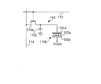
- FIG. 6 is a diagram showing an equivalent circuit of the pixel 110. The figure for demonstrating the structure of a storage area.
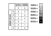
- FIG. The minimum number of voltage applications required to change the gradation is shown.
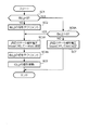
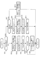
- FIG. The flowchart which showed the flow of the process which the controller 5 of a modification is performed.
- the flowchart which showed the flow of the process which the controller 5 of a modification is performed.
- the flowchart which showed the flow of the process which the controller 5 of a modification is performed.
- the flowchart which showed the flow of the process which the controller 5 of a modification is performed.
- FIG. 1 is a block diagram showing a hardware configuration of a display apparatus 1000 according to an embodiment of the present invention.
- the display device 1000 is a device that displays an image, and includes an electrophoretic electro-optical device 1, a control unit 2, a VRAM (Video Random Access Memory) 3, and a RAM 4 that is an example of a storage unit.
- the electro-optical device 1 includes a display unit 10 and a controller 5.
- the control unit 2 is a microcomputer including a CPU (Central Processing Unit), a ROM (Read Only Memory), a RAM, and the like, and controls each unit of the display device 1000.
- the control unit 2 accesses the VRAM 3 and writes image data indicating an image to be displayed in the display area 100 to the VRAM 3.
- the controller 5 supplies various signals for displaying an image on the display area 100 of the display unit 10 to the scanning line driving circuit 130 and the data line driving circuit 140 of the display unit 10.
- the controller 5 corresponds to the control device of the electro-optical device 1. Note that the combined portion of the control unit 2 and the controller 5 can be defined as the control device of the electro-optical device 1. Alternatively, the entire control unit 2, controller 5, VRAM 3, and RAM 4 can be defined as a control device for the electro-optical device 1.
- the VRAM 3 is a memory that stores image data written by the control unit 2.
- the VRAM 3 has a storage area (buffer) for each pixel 110 arranged in m rows ⁇ n columns, which will be described later.
- the image data includes pixel data representing the gradation of each pixel 110, and the pixel data representing the gradation of one pixel 110 is stored in one storage area corresponding to the pixel 110 in the VRAM 3.
- Pixel data written in the VRAM 3 is read by the controller 5.
- the RAM 4 stores various data used for displaying an image on the display area 100.
- the RAM 4 is provided with a remaining number storage area B, a gradation value storage area C, a number difference storage area D, and a scheduled image storage area E. Details of each storage area will be described later.
- a plurality of scanning lines 112 are provided along the row (X) direction in the figure, and the plurality of data lines 114 are electrically connected to each scanning line 112 along the column (Y) direction. It is provided to keep insulation. Pixels 110 are provided corresponding to the intersections of the scanning lines 112 and the data lines 114, respectively. For convenience, when the number of rows of the scanning lines 112 is “m” and the number of columns of the data lines 114 is “n”, the pixels 110 are arranged in a matrix with m rows ⁇ n columns. Will be configured.
- FIG. 2 is a view showing a cross section of the display region 100.
- the display area 100 is roughly configured by a first substrate 101, an electrophoretic layer 102, and a second substrate 103.
- the first substrate 101 is a substrate in which a circuit layer is formed on an insulating and flexible substrate 101a.
- the substrate 101a is made of polycarbonate in this embodiment. Note that the substrate 101a is not limited to polycarbonate, and a resin material having lightness, flexibility, elasticity, and insulation can be used. In addition, the substrate 101a may be formed of non-flexible glass.
- An adhesive layer 101b is provided on the surface of the substrate 101a, and a circuit layer 101c is laminated on the surface of the adhesive layer 101b.
- the circuit layer 101c has a plurality of scanning lines 112 arranged in the row direction and a plurality of data lines 114 arranged in the column direction.
- the circuit layer 101c has pixel electrodes 101d corresponding to the intersections of the scanning lines 112 and the data lines 114, respectively.
- the electrophoresis layer 102 includes a binder 102b and a plurality of microcapsules 102a fixed by the binder 102b, and is formed on the pixel electrode 101d. Note that an adhesive layer formed using an adhesive may be provided between the microcapsule 102a and the pixel electrode 101d.
- the binder 102b is not particularly limited as long as it has good affinity with the microcapsule 102a, excellent adhesion to the electrode, and has insulating properties.
- a dispersion medium and electrophoretic particles are stored in the microcapsule 102a.
- As a material constituting the microcapsule 102a it is preferable to use a flexible material such as a gum arabic / gelatin compound or a urethane compound.
- Dispersion media include water, alcohol solvents (methanol, ethanol, isopropanol, butanol, octanol, methyl cellosolve, etc.), esters (ethyl acetate, butyl acetate, etc.), ketones (acetone, methyl ethyl ketone, methyl isobutyl ketone, etc.) , Aliphatic hydrocarbons (pentane, hexane, octane, etc.), alicyclic hydrocarbons (cyclohexane, methylcyclohexane, etc.), aromatic hydrocarbons (benzene, toluene, benzenes with long chain alkyl groups (xylene) Hexylbenzene, hebutylbenzene, octylbenzene, nonylbenzene, decylbenzene, undecylbenzene, dodecylbenzene, tridecylbenzen
- Electrophoretic particles are particles (polymer or colloid) having a property of moving by an electric field in a dispersion medium.
- white electrophoretic particles and black electrophoretic particles are stored in the microcapsule 102a.
- the black electrophoretic particles are particles made of a black pigment such as aniline black or carbon black, and are positively charged in this embodiment.
- the white electrophoretic particles are particles made of a white pigment such as titanium dioxide or aluminum oxide, and are negatively charged in this embodiment.
- the second substrate 103 includes a film 103a and a transparent common electrode layer 103b (second electrode) formed on the lower surface of the film 103a.
- the film 103a plays a role of sealing and protecting the electrophoretic layer 102, and is, for example, a polyethylene terephthalate film.
- the film 103a is transparent and has an insulating property.
- the common electrode layer 103b is made of a transparent conductive film such as an indium oxide film (ITO film), for example.
- FIG. 3 is a diagram showing an equivalent circuit of the pixel 110.
- the scanning lines 112 shown in FIG. 1 are called the first, second, third,..., (M ⁇ 1), m-th rows in order from the top. You may want to Similarly, in order to distinguish the data lines 114, the data lines 114 shown in FIG. 1 are called 1, 2, 3,..., (N ⁇ 1), the nth column in order from the left. There is a case.
- FIG. 3 shows an equivalent circuit of the pixel 110 corresponding to the intersection of the scanning line 112 in the i-th row and the data line 114 in the j-th column.
- the configuration of the pixel 110 corresponding to the intersection of the other data line 114 and the scanning line 112 is the same as the configuration shown in the figure, the data line 114 in the i-th row and the scanning in the j-th column are representatively shown here.
- the equivalent circuit of the pixel 110 corresponding to the intersection with the line 112 will be described, and the description of the equivalent circuit of the other pixels 110 will be omitted.
- each pixel 110 includes an n-channel thin film transistor (hereinafter simply referred to as “TFT”) 110a, a display element 110b, and an auxiliary capacitor 110c.
- TFT thin film transistor
- the gate electrode of the TFT 110a is connected to the scanning line 112 in the i-th row
- the source electrode is connected to the data line 114 in the j-th column
- the drain electrode is a pixel that is one end of the display element 110b.
- the electrode 101d is connected to one end of the auxiliary capacitor 110c.
- the auxiliary capacitor 110c has a configuration in which a dielectric layer is sandwiched between a pair of electrodes formed on the circuit layer 101c.
- the electrode at the other end of the auxiliary capacitor 110c is set to a common voltage across the pixels.
- the pixel electrode 101d faces the common electrode layer 103b, and the electrophoretic layer 102 is sandwiched between the pixel electrode 101d and the common electrode layer 103b. Therefore, the display element 110b has a capacitance in which the electrophoretic layer 102 is sandwiched between the pixel electrode 101d and the common electrode layer 103b when viewed in an equivalent circuit.
- the display element 110b holds (stores) the voltage between both electrodes and performs display according to the direction of the electric field generated by the held voltage.
- a common voltage Vcom is applied to the electrode at the other end of the auxiliary capacitor 110c of each pixel 110 and the common electrode layer 103b by an external circuit (not shown).
- the scanning line driving circuit 130 is connected to each scanning line 112 in the display region 100.
- the scanning line driving circuit 130 selects the scanning line 112 in the order of 1, 2,..., M-th row under the control of the controller 5, and a high level signal for the selected scanning line 112. , And a low level signal is supplied to the other scanning lines 112 that are not selected.
- the data line driving circuit 140 is connected to each data line 114 in the display area, and the data line driving circuit 140 is connected to the data line 114 in each column according to the display content of one row of the pixels 110 connected to the selected scanning line 112. Each supplies a data signal.
- each period (hereinafter referred to as “frame period” or simply “frame”) after the scanning line driving circuit 130 selects the first scanning line 112 until the selection of the m-th scanning line 112 ends.
- the scanning line 112 is selected once, and a data signal is supplied to each pixel 110 once per frame.
- the TFT 110 a whose gate is connected to the scanning line 112 is turned on, and the pixel electrode 101 d is connected to the data line 114.
- a data signal is supplied to the data line 114 when the scanning line 112 is at a high level, the data signal is applied to the pixel electrode 101d through the TFT 110a that is turned on.
- the TFT 110a When the scanning line 112 becomes low level, the TFT 110a is turned off. However, the voltage applied to the pixel electrode 101d by the data signal is accumulated in the auxiliary capacitor 110c, and the potential of the pixel electrode 101d and the potential of the common electrode layer 103b. Electrophoretic particles move according to the potential difference (voltage).
- the negatively charged white electrophoretic particles move to the pixel electrode 101d side and become positive
- the charged black electrophoretic particles move to the common electrode layer 103b side, and the pixel 110 displays black.
- the positively charged black electrophoretic particles move to the pixel electrode 101d side and are negative.
- the charged white electrophoretic particles move to the common electrode layer 103b side, and the pixel 110 displays white.
- the voltage of the pixel electrode 101d is not limited to the voltage described above, and any voltage other than + 15V or ⁇ 15V described above may be used as long as the voltage is positive or negative with respect to the voltage Vcom of the common electrode layer 103b. It may be.
- each pixel 110 when the display state of each pixel 110 is changed from white (low gradation) as the first gradation to black (high gradation) as the second gradation or from black to white, one frame is used.
- the display state is changed by a writing operation for supplying the data signal to the pixel 110 over a plurality of frames. This is because when the display state is changed from white to black, even if a potential difference is applied to the electrophoretic particles for one frame, the black electrophoretic particles are not completely moved to the display side. This is because it must not.
- white electrophoretic particles when the display state is changed from black to white.
- a data signal for displaying black on the pixel 110 is supplied to the pixel 110 over a plurality of frames, and the display state of the pixel 110 is changed from black to white.
- a data signal for displaying white on the pixel is supplied to the pixel 110 over a plurality of frames.
- the pixel electrode 101d of the pixel 110 in one frame is a positive electrode whose potential is higher than that of the common electrode layer 103b, and the pixel electrode 101d of another pixel 110 in the same frame is the common electrode layer 103b.
- a negative electrode having a lower potential can be obtained. That is, the driving is such that both the positive electrode and the negative electrode can be selected with respect to the common electrode layer 103b within one frame (hereinafter referred to as bipolar driving). More specifically, in one frame, the pixel electrode 101d of the pixel 110 that changes the gradation to the high gradation side (second gradation side) is the positive electrode, and the gradation is on the low gradation side (first gradation side).
- the pixel electrode 101d of the pixel 110 to be changed is a negative electrode. Note that when the black electrophoretic particles are negatively charged and the white electrophoretic particles are positively charged, the pixel electrode of the pixel 110 that changes the gradation to the high gradation side (second gradation side). 101d may be a negative electrode, and the pixel electrode 101d of the pixel 110 whose gradation is changed to the low gradation side (first gradation side) may be a positive electrode.
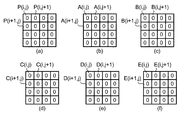
- FIG. 4 is a diagram showing a part of the pixels 110 in the display area 100 and each storage area corresponding to these pixels 110. Each storage area includes a storage area corresponding to each of the pixels 110 of m rows ⁇ n columns.
- FIG. 4A is a diagram showing the arrangement of the pixels 110.
- a pixel P (i, j) represents one pixel 110 in the i-th row and j-th column.
- the subscript i represents the row number of the pixel 110 arranged in the matrix, and the subscript j represents the column number.
- FIG. 4B is a diagram showing a buffer corresponding to each of the pixels shown in FIG.
- the buffer A (i, j) is a storage area corresponding to the pixel P (i, j).
- the buffer A (i, j) stores pixel data indicating the gradation of the pixel P (i, j). Note that pixel data whose value is “0” is written when the pixel is black, and pixel data whose value is “5” is written when the pixel is white.
- FIG. 4C is a diagram showing a storage area corresponding to each of the pixels shown in FIG.
- the remaining number storage area B (i, j) is a storage area corresponding to the pixel P (i, j).
- the remaining number storage area B (i, j) stores a value indicating the remaining number of application times when a voltage is applied to the pixel P (i, j) a plurality of times.
- FIG. 4D is a diagram showing storage areas corresponding to each of the pixels shown in FIG. 4A in the gradation value storage area C.
- the gradation value storage area C (i, j) is a storage area corresponding to the pixel P (i, j).
- the gradation value storage area C (i, j) stores a value indicating the gradation of the pixel P (i, j) that has been changed by applying a voltage.
- FIG. 4E is a diagram showing a storage area corresponding to each of the pixels shown in FIG.
- the number difference storage area D (i, j) is a storage area corresponding to the pixel P (i, j).
- the number difference storage area D (i, j) stores a value representing the difference between the number of times the positive voltage is applied and the number of times the negative voltage is applied in the pixel P (i, j).
- FIG. 4F is a diagram showing a storage area corresponding to each of the pixels shown in FIG. 4A in the scheduled image storage area E.
- the scheduled image storage area E (i, j) is a storage area corresponding to the pixel P (i, j).
- pixel data of each pixel of an image scheduled to be displayed in the display area 100 is stored.
- FIG. 5 is a block diagram showing functions realized in the controller 5.
- a frequency difference calculation unit 501 a voltage control unit 502, and an application frequency determination unit 503 are realized.
- Each of these blocks may be realized by hardware, or each block may be realized by providing a CPU in the controller 5 and executing a program by this CPU.
- the number difference calculation unit 501 is a block that calculates the number difference for each pixel. When the second voltage is applied to the pixel electrode 101d of the pixel P (i, j) corresponding to the number difference storage area D (i, j), the number difference calculation unit 501 counts the number difference storage area D (i, j).
- the frequency difference calculation unit 501 writes the difference between the number of times of applying the first voltage and the number of times of applying the second voltage in the frequency difference storage area D (i, j).
- the voltage control unit 502 When the value of the remaining number storage area B (i, j) is 0 and the value of the number difference storage area D (i, j) is not a predetermined value, the voltage control unit 502 counts the number difference storage area.
- the scanning line driving circuit 130 and the data line driving circuit 140 are controlled to apply the first voltage or the second voltage to the pixel electrode 101d until the value of D (i, j) reaches a predetermined value. Further, the voltage control unit 502 determines that the value of the number difference storage area D (i, j) is not a predetermined value at a timing when the value of the buffer A (i, j) and the value of the scheduled image storage area E (i, j) are different.
- the first voltage or the second voltage is applied to the pixel electrode 101d by controlling the scanning line driving circuit 130 and the data line driving circuit 140 until the value of the number difference storage area D (i, j) reaches a predetermined value.
- the voltage control unit 502 controls the scanning line driving circuit 130 and the data line driving circuit 140 based on the value of the scheduled image storage area E (i, j) and the value of the remaining number of times storage area B (i, j). Then, the first voltage or the second voltage is applied to the pixel electrode 101d.
- the voltage control unit 502 when changing the gradation of a pixel before the voltage application to the pixel is completed a plurality of times, the voltage control unit 502 newly performs an operation to apply the voltage to the pixel a plurality of times even during the writing operation. Start.
- the number-of-applications determination unit 503 determines the level of the pixel P (i, j) based on the value of the gradation value storage area C (i, j), the value of the buffer A (i, j), and the table of FIG. This block determines the number of times of application of the first voltage or the second voltage for changing the key.
- the application frequency determination unit 503 writes the determined application frequency in the remaining frequency storage area B (i, j).
- FIG. 6 is a diagram showing the minimum number of voltage applications required to change the gradation.
- the controller 5 stores the table shown in FIG.
- the gradation of the pixel 110 changes in 6 steps from 0 to 5, and the smaller the gradation value, the higher the density.
- the gradation value is 0, black, the gradation value is 5. In this case, it is defined as white. According to FIG.
- the image can be rewritten quickly.
- the number of times the voltage is applied is different. Therefore, when the image is rewritten repeatedly, a positive voltage is applied to the common electrode layer 103b.
- the microcapsule is quickly deteriorated due to the deviation between the number of times of application and the number of times of applying a negative voltage to the common electrode layer 103b.
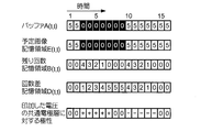
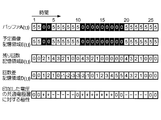
- FIG. 11 is a diagram showing the contents of each storage area that changes over time.
- the buffer A (1,1) corresponding to one pixel P (1,1) and the remaining number storage area B ( 1, 1), the gradation value storage area C (1,1), the number difference storage area D (1,1), and the scheduled image storage area E (1,1).
- the contents of each storage area are values after the end of the frame period.
- FIG. 11 also shows the polarity of the voltage applied to the pixel electrode 101d in one frame period with respect to the common electrode layer 103b.
- the buffer A (1,1) is 5
- the gradation value storage area C (1,1) is 5
- D (1,1) is 0.
- the voltage applied to the pixel electrode 101d is the same as the voltage Vcom, and the value of each storage area does not change.
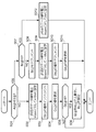
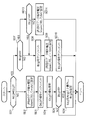
- the controller 5 performs the process of FIG. 7 before the start of the frame period. Specifically, the controller 5 rewrites the contents of the remaining number storage area B and the scheduled image storage area E according to the contents of each storage area.
- the controller 5 initializes variable i and variable j to 1 (steps SA1 and SA2).
- the controller 5 determines whether the value of the buffer A (i, j) and the value of the scheduled image storage area E (i, j) are the same.
- step SA3 if the value of the buffer A (i, j) and the value of the scheduled image storage area E (i, j) are the same (YES in step SA3), the controller 5 moves the process flow to step SA9.
- the controller 5 has the remaining number storage area B (i, j) of 0. It is judged whether it is.
- the controller 5 stores the buffer A (i, j), the gradation value storage area C (i, j), and the table of FIG.
- step SA5 the controller 5 overwrites the value of the scheduled image storage area E (i, j) with the value of the buffer A (i, j).
- the controller 5 determines whether the value of the buffer A (i, j) is 5 (white) when the value of the remaining number storage area B (i, j) is not 0 (NO in step SA4). If the value of the buffer A (i, j) is not 5 (NO in step SA7), the controller 5 moves the process flow to step SA5. On the other hand, when the value of the buffer A (i, j) is 5 (YES in step SA7), the controller 5 determines the value of the number difference storage area D (i, j) as a predetermined threshold value (in this embodiment).
- step SA7 It is determined whether or not (in other words, if the value of the buffer A (i, j) is 5 (YES in step SA7), the controller 5 determines the value of the number difference storage area D (i, j)) It is determined whether the absolute value of is greater than or equal to a predetermined threshold value of 4). If the value of the number-of-times difference storage area D (i, j) is not less than or equal to the threshold value (NO in step SA8), the controller 5 moves the process flow to step SA5. On the other hand, when the value of the number difference storage area D (i, j) is equal to or less than the threshold value (YES in step SA8), the controller 5 moves the process flow to step SA9.
- Controller 5 determines whether the value of variable j is n in step SA9. If the value of the variable j is not n, the controller 5 increments the variable j and moves the process flow to step SA3. If the value of variable j is n, controller 5 determines whether the value of variable i is m in step SA10. If the value of the variable i is not m, the controller 5 increments the variable i and moves the process flow to step SA2. Moreover, the controller 5 complete
- the controller 5 rewrites the buffer A (1,1) from 5 to 0 before the start of the third frame, and the value of the buffer A (1,1) changes to the scheduled image storage area E (before the start of the third frame. If it is different from the value (5) of (1,1) (NO in step SA3), it is determined whether the remaining number storage area B (1,1) is zero. Here, as shown in FIG. 11, if the remaining number storage area B (1,1) is 0 before the start of the third frame (YES in step SA4), the controller 5 determines that the pixel P (1,1 The number of times of voltage application necessary for changing the gradation of 5) from 5 to 0 is written in the remaining number storage area B (1, 1) (step SA5). Referring to FIG.
- the controller 5 writes 3 in the remaining number of times of storage area B (1,1). Further, the controller 5 overwrites the value of the scheduled image storage area E (i, j) with 0 which is the value of the buffer A (i, j) (step SA6).
- the controller 5 drives the scanning line driving circuit 130 and the data line driving circuit 140 when the frame period comes after the processing of FIG.
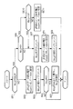
- the controller 5 performs the processes of FIGS. 8 to 10 when driving the data line driving circuit.
- the controller 5 initializes variable i and variable j to 1 (steps SB1 and SB2).
- the controller 5 determines whether or not the value of the buffer A (i, j) is zero. If the value of the buffer A (i, j) is 0 (black) (YES in step SB3), the controller 5 performs the process shown in FIG. 9 in step SB4.
- the controller 5 determines whether the value of the remaining number storage area B (i, j) is zero.
- step SC1 When the value of the remaining number storage area B (i, j) is not 0 (NO in step SC1), the controller 5 decrements the value of the remaining number storage area B (i, j) (step SC2). Further, the controller 5 sets the data line 114 in the jth column to + 15V with respect to the voltage Vcom (step SC3), and increments the value of the number difference storage area D (i, j) (step SC4). Next, the controller 5 updates the value of the gradation value storage area C (i, j) (step SC5), and moves the process flow to step SC6.
- step SC1 determines whether the value of the remaining number storage area B (i, j) is 0 (YES in step SC1). If the value of the number difference storage area D (i, j) is less than 5 (YES in step SC6), the controller 5 moves the process flow to step SC3. When the value of the number-of-times difference storage area D (i, j) is equal to or greater than a predetermined threshold value (here, 5) (NO in step SC6), the controller 5 connects the j-th data line 114 to the voltage Vcom. To 0V (step SC7), and the flow of processing moves to step SB6.
- a predetermined threshold value here, 5
- the controller 5 when the value of the buffer A (i, j) is 5 (white) (NO in step SB3), the controller 5 performs the process of FIG. The controller 5 determines whether the value of the buffer A (i, j) and the value of the scheduled image storage area E (i, j) are the same. When the value of the buffer A (i, j) is different from the value of the scheduled image storage area E (i, j) (NO in step SD1), the controller 5 sets the data line 114 in the jth column to + 15V with respect to the voltage Vcom. (Step SD2), and the value of the number-of-times difference storage area D (i, j) is incremented (step SD3).
- the controller 5 updates the value of the gradation value storage area C (i, j) (step SD4).
- step SD5 when the value of the number difference storage area D (i, j) is 5 (YES in step SD5), the controller 5 stores the value of the scheduled image storage area E (i, j) in the buffer A (i, j). Is overwritten with the value of (step SD6).
- step SD6 After finishing the process of step SD6, the controller 5 moves the process flow to step SB6. If the value of the number difference storage area D (i, j) is not 5 (NO in step SD5), the controller 5 moves the process flow to step SB6.
- step SD1 determines whether the value of the remaining number storage area B (i, j) is zero. When the value of the remaining number storage area B (i, j) is 0 (YES in step SD7), the controller 5 sets the data line 114 in the j-th column to 0 V with respect to the voltage Vcom (step SD12), The flow is moved to step SB6.
- step SD7 the controller 5 decrements the value of the remaining number of storage areas B (i, j) (step SD8).
- step SD9 the controller 5 sets the data line 114 in the j-th column to ⁇ 15 V with respect to the voltage Vcom (step SD9), and decrements the value of the number difference storage area D (i, j) (step SD10).
- step SD11 the controller 5 updates the value of the gradation value storage area C (i, j) (step SD11). After finishing the process of step SD11, the controller 5 moves the process flow to step SB6.
- the controller 5 determines whether or not the value of the variable j is n in Step SB6. If the value of the variable j is not n, the controller 5 increments the variable j and moves the process flow to step SB3. Further, when the value of the variable j is n, the controller 5 drives the i-th scanning line (step SB7). Next, the controller 5 determines whether the value of the variable i is m in step SB8. If the value of the variable i is not m, the controller 5 increments the variable i and moves the process flow to step SB2. Moreover, the controller 5 complete
- the controller 5 has a buffer A (1,1) value of 0 (YES in step SB3) and the remaining number storage area B (1,1) has a value of 3. Because there is (NO in step SC1), the value of the remaining number of times storage area B (1,1) is decremented to 2 (step SC2).
- the controller 5 sets the data line 114 in the first column to +15 V with respect to the voltage Vcom (step SC3), and then increments the value of the number difference storage area D (1,1) to 1 (step SC4).
- the controller 5 updates the value of the gradation value storage area C (1,1) (step SC5).
- step SB7 when a voltage of +15 V is applied to the pixel electrode 101d with respect to the voltage Vcom, the actual change in the gradation value of the pixel due to one voltage application is 2, so when the third frame ends, The gradation value in the gradation value storage area C (1,1) is 3. Thereafter, when the scanning line 112 in the first row is driven (step SB7), a voltage of + 15V with respect to the voltage Vcom is applied to the pixel electrode 101d of the pixel in the first row and the first column, and black electrophoresis is performed. The particles move to the common electrode layer 103b side.
- the controller 5 performs the same process as the third frame in the fourth and fifth frames.
- the operation of the controller 5 is as follows. First, since the value of the buffer A (1,1) is 0 (YES in step SB3) and the value of the remaining number storage area B (1,1) is 0 (YES in step SC1), the controller 5 The value of the number difference storage area D (1,1) is determined. Here, since the value of the number difference storage area D (1,1) is 3 and the value is less than 5 (YES in step SC6), the data line 114 in the first column is set to + 15V with respect to the voltage Vcom. Later (step SC3), the value of the number difference storage area D (1,1) is incremented to 4 (step SC4). Further, the controller 5 updates the value of the gradation value storage area C (1,1) (step SC5). Here, when the value of the gradation value storage area C (1,1) is 0, the value remains 0.
- the controller 5 performs the same process as the sixth frame in the seventh frame.
- the operation of the controller 5 is as follows. First, since the value of the buffer A (1,1) is 0 (YES in step SB3) and the value of the remaining number storage area B (1,1) is 0 (YES in step SC1), the controller 5 The value of the number difference storage area D (1,1) is determined. Here, since the value of the number difference storage area D (1,1) is 5 (NO in step SC6), the data line 114 in the first column is set to 0 V with respect to the voltage Vcom (step SC7).
- the operation of the controller 5 is as follows.
- the controller 5 stores the remaining number of times because the value of the buffer A (1,1) is different from the value (0) of the scheduled image storage area E (1,1) before the start of the tenth frame (NO in step SA3). It is determined whether the area B (1, 1) is zero.
- the area B (1, 1) is zero.
- step SA4 when the remaining number storage area B (1,1) is 0 at the time before the start of the 10th frame (at the end of the 9th frame) (YES in step SA4), the controller 5 writes the number of voltage application necessary to change the gradation of the pixel P (1,1) from 5 to 0 in the remaining number storage area B (1,1) (step SA5).
- step SA5 since the number of voltage applications necessary to change the gradation of the pixel from 5 to 0 is 3, the controller 5 writes 3 in the remaining number storage area B (1, 1).
- the controller 5 overwrites the value of the scheduled image storage area E (i, j) with 5 which is the value of the buffer A (i, j) (step SA6).
- the controller 5 determines whether the value of the buffer A (i, j) is zero or not. If the value of the buffer A (i, j) is 5 (white) (NO in step SB3), the controller 5 performs the process shown in FIG. First, the controller 5 has the same value in the buffer A (i, j) as the value in the scheduled image storage area E (i, j) (YES in step SD1), and the value in the remaining number storage area B (i, j). Is not 0 (NO in step SD7), the value of the remaining number of storage areas B (1,1) is decremented to 4 (step SD8).
- the controller 5 sets the data line 114 in the first column to ⁇ 15 V with respect to the voltage Vcom (step SD9), and then decrements the value of the number difference storage area D (1,1) to 4 (step SD10). ). Further, the controller 5 updates the value of the gradation value storage area C (1,1) (step SD11). Note that when a voltage of ⁇ 15 V is applied to the pixel electrode 101d with respect to the voltage Vcom, the actual change in the gradation value of the pixel due to a single voltage application is 1, so when the 10th frame is completed, The gradation value in the gradation value storage area C (1,1) is 4.
- step SB7 a voltage of ⁇ 15V with respect to the voltage Vcom is applied to the pixel electrode 101d of the pixel in the first row and the first column, and white electrical The migrating particles move to the common electrode layer 103b side.
- the controller 5 applies a voltage to the pixel electrode 101d in each frame period until the value of the remaining number storage area B (1,1) becomes zero.
- the controller 5 applies the same voltage as the voltage Vcom to the pixel electrode 101d in the 15th frame when the content of the remaining number storage area B (1,1) becomes 0 at the start time of the 15th frame.
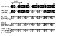
- FIG. 12 is also a diagram showing the contents of each storage area that changes over time.
- the buffer A (1,1) corresponding to the pixel P (1,1) and the remaining number storage area B (1,1) are also shown.
- the contents of the gradation value storage area C (1,1) and the number difference storage area D (1,1) are shown.
- the operation from the first frame to the fourth frame is the same as the operation from the first frame to the fourth frame in FIG.
- the controller 5 sets the gradation of the pixel 110 in the buffer A (1,1) before the fifth frame before the value of the remaining number storage area B (1,1) becomes 0 for the pixel P (1,1).
- NO is determined in step SA3
- NO is determined in step SA4.
- the controller 5 stores the remaining number of times storage area in step SA5. 4 is written to B (1,1), and 5 is written to the scheduled image storage area E (1,1) in step SA6.
- the controller 5 sets the voltage of the pixel electrode 101d of the pixel P (1,1) to ⁇ 15V with respect to the voltage Vcom from the fifth frame to the eighth frame.
- the controller 5 sets the voltage of the pixel electrode 101d of the pixel P (1,1) to the same voltage as the voltage Vcom. To do.
- the controller 5 stores the difference in the number of times as in the third and subsequent frames in FIG.
- the voltage of the pixel electrode 101d of the pixel P (1,1) is set to + 15V with respect to the voltage Vcom until the value of the region D (1,1) becomes 5.
- 5 (white) is written as the gradation value of the pixel 110 in the buffer A (1,1) before the 20th frame
- the controller 5 stores the remaining number of times as in the 10th and subsequent frames in FIG.
- the voltage of the pixel electrode 101d of the pixel P (1,1) is set to ⁇ 15V with respect to the voltage Vcom until the value of the region B (1,1) becomes zero.
- FIG. 13 is also a diagram showing the contents of each storage area that changes over time.
- the buffer A (1,1) corresponding to the pixel P (1,1) and the remaining number storage area B (1,1) are also shown.
- the contents of the gradation value storage area C (1,1) and the number difference storage area D (1,1) are shown.
- the operation from the first frame to the twelfth frame in FIG. 13 is the same as the operation from the first frame to the twelfth frame in FIG.
- the controller 5 performs the same operation as the operation from the fifth frame to the eighth frame when 5 (white) is written as the gradation value of the pixel 110 in the buffer A (1,1) before the 13th frame.
- the controller 5 writes 0 (black) as the gradation value of the pixel 110 in the buffer A (1,1) before the 19th frame, and the pixel 110 in the buffer A (1,1) before the 21st frame.
- 5 (white) is written as the gradation value of
- the same operation as the operation from the third frame to the eighth frame is performed from the 19th frame to the 24th frame.
- the controller 5 sets the third and fourth frames for the 27th and 28th frames. Performs the same operation as the frame.
- step SA7 when 5 (white) is written as the gradation value of the pixel 110 in the buffer A (1,1) before the 29th frame, the controller 5 determines NO in step SA3 and NO in step SA4. to decide. Further, since the value of the buffer A (1,1) is 5 (YES in step SA7), the controller 5 determines the value of the number difference storage area D (1,1). Here, since the value of the number difference storage area D (1,1) is ⁇ 4, the controller 5 determines YES in step SA8 and does not update the contents of the scheduled image storage area E (1,1).
- step SB5 because the value of the buffer A (1, 1) is 5.
- the controller 5 connects the data line 114 in the first column to the voltage Vcom.
- the controller 5 also updates the value of the gradation value storage area C (1,1) to 0.
- the controller 5 determines whether or not the value of the number difference storage area D (1,1) is 5.
- step SD5 NO is determined in step SD5
- step SD5 NO is determined in step SD5
- step SD5 NO is determined in step SD5
- step SD5 the value of the scheduled image storage area E (1,1) remains zero.
- step SB7 when the scanning line 112 in the first row is driven (step SB7), a voltage of + 15V with respect to the voltage Vcom is applied to the pixel electrode 101d of the pixel in the first row and the first column, and the buffer A (1 , 1) is 5, which represents white as the pixel gradation, but the black electrophoretic particles move to the common electrode layer 103b side.
- Controller 5 performs the same operation as the 29th frame for pixel P (1,1) from the 30th frame to the 36th frame. Since the value of the buffer A (1,1) and the value of the scheduled image storage area E (1,1) are different in the 37th frame (NO in step SD1), the controller 5 sets the data line 114 in the first column. After setting the voltage Vcom to + 15V (step SD2), the value of the number difference storage area D (1,1) is incremented to 5. Thereafter, since the value of the number difference storage area D (1,1) is 5 (NO in step SD5), the controller 5 stores the value of the scheduled image storage area E (1,1) in the buffer A (1,1). ) Value 5 is overwritten, and the remaining number of times storage area B (1,1) is stored based on the buffer A (1,1), the gradation value storage area C (1,1) and the table of FIG. Write the value.
- step SB5 Since the value of the buffer A (1,1) is 5 at the 38th frame, the controller 5 performs the process of step SB5. Since the value of the buffer A (1,1) and the value of the scheduled image storage area E (1,1) are the same and the value of the remaining number of times storage area B (1,1) is not 0, the controller 5 The processing from SD8 to step SD11 is performed. That is, a voltage of ⁇ 15V with respect to the voltage Vcom is applied to the pixel electrode 101d of the pixel in the first row and the first column. Thereafter, the controller 5 applies a voltage of ⁇ 15 V to the voltage Vcom for the pixel electrode 101d of the pixel P (1,1) until the 42nd frame.
- the buffer A (1,1) is rewritten and a voltage of ⁇ 15V is applied to the voltage Vcom to the pixel electrode 101d of the pixel P (1,1) from the 29th frame, the number-of-times difference storage area D
- the absolute value of the (1,1) value is further increased. That is, in the pixel P (1,1), there is a large deviation between the number of times that the positive voltage is applied to the common electrode layer 103b and the number of times that the negative voltage is applied to the common electrode layer 103b. Will occur and the pixel 110 will deteriorate quickly.
- the voltage applied to the pixel electrode 101d is controlled and is positive with respect to the common electrode layer 103b.
- a large deviation does not occur between the number of times a voltage is applied and the number of times a negative voltage is applied to the common electrode layer 103b, so that deterioration of the pixel 110 can be suppressed.
- the display device according to the second embodiment has the same hardware configuration as that of the first embodiment.
- the display device according to the second embodiment is different from the display device according to the first embodiment in that the gradation value storage area C is not provided and the processing performed by the controller 5 is different.
- this difference will be mainly described.
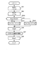
- FIG. 14 to 16 are flowcharts showing the flow of processing performed by the controller 5.
- FIG. 14 is a diagram showing a flow of processing performed by the controller 5 when the contents of the VRAM 3 are rewritten.
- FIG. 14 is different from the process of FIG. 7 of the first embodiment in that step SA11 is provided.
- the controller 5 determines that the value of the buffer A (i, j) is different from the value of the scheduled image storage area E (i, j), the value of the remaining number storage area B (i, j) is not 0, and the buffer A (i , j) is 0, it is determined in step SA11 whether the value of the number-of-times difference storage area D (i, j) is 4 or more.
- step SA11 When the value of the number difference storage area D (i, j) is less than a predetermined threshold (here, 4) in step SA11, the controller 5 moves the process flow to step SA5, and stores the number difference storage in step SA11. If the value of the area D (i, j) is 4 or more, the flow of processing moves to step SA9.
- a predetermined threshold here, 4
- FIG. 15 is a flowchart showing a process flow of step SB4 (subroutine 1) according to the present embodiment.
- the controller 5 determines whether the value of the buffer A (i, j) and the value of the scheduled image storage area E (i, j) are the same.
- step SE1 When the value of the buffer A (i, j) is different from the value of the scheduled image storage area E (i, j) (NO in step SE1), the controller 5 sets the jth data line 114 to the voltage Vcom ⁇ The voltage is set to 15 V (step SE2), and the value of the number difference storage area D (i, j) is decremented (step SE3). If the value of the number difference storage area D (i, j) is 0 (YES in step SE4), the controller 5 stores the value of the scheduled image storage area E (i, j) in the buffer A (i, j). Is overwritten with the value of (step SE5). When the process of step SE5 is completed, the controller 5 moves the process flow to step SB6. If the value of the number difference storage area D (i, j) is not 0 (NO in step SE4), the controller 5 moves the process flow to step SB6.
- step SE1 determines whether or not the value of the remaining number storage area B (i, j) is zero. If the value of the remaining number storage area B (i, j) is 0 (YES in step SE6), the controller 5 determines whether the value of the number difference storage area D (i, j) is less than 5.
- step SE10 If the value of the number difference storage area D (i, j) is less than 5 (YES in step SE10), the controller 5 moves the process flow to step SE7, and the value of the number difference storage area D (i, j) Is not less than 5 (NO in step SE10), the data line 114 in the j-th column is set to 0 V with respect to the voltage Vcom (step SE11), and the process flow proceeds to step SB6.
- step SE6 the controller 5 decrements the value of the remaining number of storage areas B (i, j) (step SE7).
- step SE8 the controller 5 sets the data line 114 in the j-th column to +15 V with respect to the voltage Vcom (step SE8), and decrements the value of the number difference storage area D (i, j) (step SE9).
- step SB6 the controller 5 moves the process flow to step SB6.
- FIG. 16 is a flowchart showing a process flow of step SB5 (subroutine 2) according to the present embodiment.
- the process of step SD4 and step SD11 is different from the first embodiment in that the process of step SD4 and step SD11 is not provided, and the process of step SD13 and step SD14 is provided. Is done.
- the process of step SD14 is the same process as step SD12 of the first embodiment.
- step SD13 When the value of the number difference storage area D (i, j) exceeds 0 in step SD13 (YES in step SD13), the controller 5 moves the flow of processing to step SD8, where the number difference storage area D (i, j, If the value of j) is 0 or less (NO in step SD13), the data line 114 in the j-th column is set to 0V with respect to the voltage Vcom (step SE11), and the process flow proceeds to step SB6.
- FIG. 17 is a diagram showing the contents of each storage area that changes over time.
- the buffer A (1,1) corresponding to the pixel P (1,1) and the remaining number of storage areas B (1,1) are shown.
- the contents of the number difference storage area D (1,1) and the scheduled image storage area E (1,1) are shown.
- the contents of each storage area are values after the end of the frame period.
- FIG. 17 also shows the polarity of the voltage applied to the pixel electrode 101d in one frame period with respect to the common electrode layer 103b.
- the controller 5 performs the process of FIG. 14 before the start of the frame period.
- the controller 5 writes 5 in the remaining number of times storage area B (1,1) and 0 in the scheduled image storage area E (1,1) in step SA5. .
- this embodiment is different from the first embodiment in that 5 is written without using the table of FIG.
- the controller 5 applies a voltage of + 15V to the voltage Vcom to the pixel electrode 101d of the pixel P (1,1), and the value of the remaining number storage area B (1,1) Is decremented, and the value of the count difference storage area D (1,1) is incremented.
- the controller 5 has the same values in the buffer A (1,1) and the scheduled image storage area E (1,1) in the eighth and ninth frames, and the remaining number of storage areas B (1,1). Since the value is 0, the voltage of the pixel electrode 101d of the pixel P (1,1) is made the same as the voltage Vcom.
- the controller 5 If the buffer A (1,1) is rewritten from 5 to 0 before the start of the 10th frame, the controller 5 writes 5 to the remaining number of times storage area B (1,1) in step SA5, and the scheduled image storage area Write 5 to E (1,1). From the 10th frame to the 14th frame, the controller 5 applies a voltage of ⁇ 15V to the voltage Vcom to the pixel electrode 101d of the pixel P (1,1), and stores the remaining number of times in the storage area B (1,1). The value is decremented, and the value in the count difference storage area D (1,1) is decremented.
- FIG. 18 is also a diagram showing the contents of each storage area corresponding to the pixel P (1,1).
- the operation from the first frame to the fourth frame is the same as the operation from the fourth frame in FIG.
- the controller 5 performs the process of FIG. 14 before the start of the frame period.
- the controller 5 pays attention to the pixel P (1,1), the controller 5 writes 5 in the remaining number of times storage area B (1,1) and writes 5 in the scheduled image storage area E (1,1) in step SA5. .
- the controller 5 sets the gradation of the pixel 110 in the buffer A (1,1) before the fifth frame before the value of the remaining number storage area B (1,1) becomes 0 for the pixel P (1,1).
- NO is determined in step SA3
- NO is determined in step SA4.
- the controller 5 stores the remaining number of times storage area in step SA5. 5 is written in B (1,1), and 5 is written in the scheduled image storage area E (1,1) in step SA6.
- the controller 5 sets the voltage of the pixel electrode 101d of the pixel P (1,1) to ⁇ 15V with respect to the voltage Vcom from the fifth frame to the ninth frame.
- the controller 5 sets the voltage of the pixel electrode 101d of the pixel P (1,1) to the same voltage as the voltage Vcom.
- the controller 5 sets the remaining number of times storage area B (i, j) to 0.
- the voltage of the pixel electrode 101d of the pixel P (1,1) is set to + 15V with respect to the voltage Vcom until Further, the controller 5 sets the voltage of the pixel electrode 101d of the pixel P (1, 1) to + 15V with respect to the voltage Vcom until the value of the number-of-times difference storage area D (i, j) becomes 5.
- the controller 5 stores the remaining number of times as in the 10th frame and after in FIG.
- the voltage of the pixel electrode 101d of the pixel P (1,1) is set to ⁇ 15V with respect to the voltage Vcom until the value of the region B (1,1) becomes zero.
- FIG. 19 is also a diagram showing the contents of each storage area corresponding to the pixel P (1,1).
- the operation from the first frame to the twelfth frame in FIG. 19 is the same as the operation from the first frame to the twelfth frame in FIG.
- the controller 5 When 5 (white) is written as the gradation value of the pixel 110 in the buffer A (1,1) before the 13th frame, the controller 5 operates from the 5th frame to the 9th frame. Perform the same operation. Further, when 0 (black) is written as the gradation value of the pixel 110 in the buffer A (1,1) before the 19th frame, the controller 5 sets the 3rd and 4th frames for the 19th and 20th frames. Performs the same operation as the frame.
- step SA3 when 5 (white) is written as the gradation value of the pixel 110 in the buffer A (1,1) before the 21st frame, the controller 5 determines NO in step SA3, and determines NO in step SA4. to decide. Further, since the value of the buffer A (1,1) is 5 (YES in step SA7), the controller 5 determines the value of the number difference storage area D (1,1). Here, since the value of the number difference storage area D (1,1) is ⁇ 4, the controller 5 determines YES in step SA8 and does not update the contents of the scheduled image storage area E (1,1).
- step SB5 the controller 5 performs the process of step SB5 because the value of the buffer A (i, j) is 5.
- the controller 5 connects the data line 114 in the first column to the voltage Vcom.
- the controller 5 determines whether or not the value of the number difference storage area D (1,1) is 5.
- NO is determined in step SD5
- the value of the scheduled image storage area E (1,1) remains zero.
- step SB7 when the scanning line 112 in the first row is driven (step SB7), a voltage of + 15V with respect to the voltage Vcom is applied to the pixel electrode 101d of the pixel in the first row and the first column, and the buffer A (1 , 1) is 5, which represents white as the pixel gradation, but the black electrophoretic particles move to the common electrode layer 103b side.
- the controller 5 performs the same operation as the 21st frame for the pixel P (1,1) from the 22nd frame to the 28th frame. Since the value of the buffer A (1,1) and the value of the scheduled image storage area E (1,1) are different in the 29th frame (NO in step SD1), the controller 5 sets the data line 114 in the first column. After setting the voltage Vcom to + 15V (step SD2), the value of the number difference storage area D (1,1) is incremented to 5. Thereafter, since the value of the number difference storage area D (1,1) is 5 (NO in step SD5), the controller 5 stores the value of the scheduled image storage area E (1,1) in the buffer A (1,1). ) Is overwritten with 5 which is the value of), and 5 is written into the remaining number of times storage area B (1,1).
- the controller 5 performs the process of step SB5 because the value of the buffer A (1,1) is 5 in the 30th frame. Since the value of the buffer (1,1) and the value of the scheduled image storage area E (1,1) are the same and the value of the remaining number of times storage area B (1,1) is not 0, the controller 5 performs step SD8. Process of step SD10 is performed. That is, a voltage of ⁇ 15V with respect to the voltage Vcom is applied to the pixel electrode 101d of the pixel in the first row and the first column. Thereafter, the controller 5 applies a voltage of ⁇ 15V to the voltage Vcom for the pixel electrode 101d of the pixel P (1, 1) until the 34th frame.
- FIG. 20 is also a diagram showing the contents of each storage area corresponding to the pixel P (1,1).
- the buffer A (1,1) is 0, the gradation value storage area C (1,1) is 0, the remaining number storage area B (1,1) and the number difference storage area. D (1,1) is 5.
- the voltage applied to the pixel electrode 101d is the same as the voltage Vcom, and the value of each storage area does not change.
- the buffer A (1,1) is rewritten from 0 to 5 before the start of the third frame, and the value of the buffer A (1,1) becomes the scheduled image storage area E (1,1) before the start of the third frame. (0 in step SA3), it is determined whether or not the remaining number storage area B (1, 1) is zero.
- the controller 5 uses the pixel P (1,1). ) Is written in the remaining number storage area B (1,1) as the number of times of voltage application necessary to change the gradation of 0) from 0 to 5 (step SA5).
- the controller 5 overwrites the value of the scheduled image storage area E (i, j) with 5 which is the value of the buffer A (i, j) (step SA6).
- the controller 5 drives the scanning line driving circuit 130 and the data line driving circuit 140 in the frame period.
- the controller 5 has a buffer A (1,1) value of 5 (NO in step SB3), and the buffer A (1,1) and the scheduled image storage area E (1,1) have the same value (YES in step SD1). Since the value of the remaining number storage area B (1,1) is 5 (NO in step SD7), the value of the remaining number storage area B (1,1) is decremented to 4 (step SD8).
- the controller 5 sets the data line 114 in the first column to ⁇ 15V with respect to the voltage Vcom (step SD9), and then decrements the value of the number difference storage area D (1,1) to 4 (step SD10). .
- the controller 5 sets the gradation of the pixel 110 in the buffer A (1,1) before the fifth frame before the value of the remaining number storage area B (1,1) becomes 0 for the pixel P (1,1).
- NO black
- NO determined in step SA3
- NO is determined in step SA4.
- the controller 5 stores the remaining number of times storage area in step SA5. 5 is written in B (1,1), and 0 is written in the scheduled image storage area E (1,1) in step SA6.
- the controller 5 sets the voltage of the pixel electrode 101d of the pixel P (1,1) to + 15V with respect to the voltage Vcom from the fifth frame to the ninth frame.
- the controller 5 sets the voltage of the pixel electrode 101d of the pixel P (1,1) to the same voltage as the voltage Vcom.
- the controller 5 sets the 3rd and 4th frames in the 11th and 12th frames. Similarly to the eye, the voltage of the pixel electrode 101d of the pixel P (1,1) is set to ⁇ 15V with respect to the voltage Vcom. Further, when 0 (black) is written as the gradation value of the pixel 110 in the buffer A (1,1) before the 13th frame, the controller 5 determines NO in step SA3 and determines NO in step SA4. To do. Further, since the value of the buffer A (1,1) is 0 (NO in step SA7), the controller 5 determines the value of the number difference storage area D (1,1). Here, since the value of the number difference storage area D (1,1) is 7, the controller 5 determines YES in step SA11 and does not update the contents of the scheduled image storage area E (1,1).
- step SB4 the controller 5 performs the process of step SB4 because the value of the buffer A (i, j) is 0.
- the controller 5 sets the data line 114 in the first column to the voltage Vcom.
- the value of the number difference storage area D (1,1) is decremented to 6.
- the controller 5 determines whether or not the value of the number-of-times difference storage area D (1,1) is zero.
- step SE4 NO is determined in step SE4, and the value of the scheduled image storage area E (1,1) remains at 5.
- step SB7 when the first scanning line 112 is driven (step SB7), a voltage of ⁇ 15V with respect to the voltage Vcom is applied to the pixel electrode 101d of the pixel in the first row and first column, and the buffer A ( The value of 1,1) is 0 representing black as the pixel gradation, but the white electrophoretic particles move to the common electrode layer 103b side.
- step SE4 determines YES in step SE4, writes 5 in the remaining number of times storage area B (i, j), and stores the value of the scheduled image storage area E (i, j) in the buffer A (i , j) Overwrite with value. Since the value of the buffer A (1,1) is 0 in the 20th frame, the controller 5 performs the process of step SB4.
- step SE7 Since the value of the buffer (1,1) and the value of the scheduled image storage area E (1,1) are the same and the value of the remaining number of times storage area B (1,1) is not 0, the controller 5 is step SE7. Process of step SE9 is performed. That is, a voltage of + 15V with respect to the voltage Vcom is applied to the pixel electrode 101d of the pixel in the first row and the first column. Thereafter, the controller 5 applies a voltage of +15 V to the voltage Vcom for the pixel electrode 101d of the pixel P (1,1) until the 24th frame.
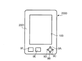
- FIG. 21 is a diagram illustrating an appearance of an electronic book reader using the electro-optical device 1.
- the electronic book reader 2000 includes a plate-shaped frame 2001, buttons 9A to 9F, the electro-optical device 1, the control unit 2, the VRAM 3, and the RAM 4 according to the above-described embodiment.
- the display area 100 is exposed.
- the contents of the electronic book are displayed in the display area 100, and the pages of the electronic book are turned by operating the buttons 9A to 9F.
- examples of the electronic apparatus to which the electro-optical device 1 according to the above-described embodiment can be applied include a watch, electronic paper, an electronic notebook, a calculator, a mobile phone, and the like.
- the number of times of voltage application when rewriting a pixel may be changed according to the temperature around the pixel 110.
- the number of voltage applications may be decreased when the temperature is high, and the number of voltage applications may be increased when the temperature is low.
- the values used in the determination processing such as Step SA8, Step SC6, Step SD5, etc. of the first embodiment may be changed according to the temperature. Good.
- the values used in the determination processing in step SA8, step SA11, step SE4, step SD5, etc. of the second embodiment are also changed according to the temperature. May be.
- the number of times of voltage application from black to white is three, and the number of times of voltage application from white to black is five. It may also occur when the number of times of voltage application from white to black is larger.
- the processes in FIGS. 22 to 25 are performed instead of the processes in FIGS.
- the process of FIG. 22 if the value of buffer A (i, j) is 5 (white) in step SA7A, the process proceeds to step SA5, and if the value is 0 (black), the process proceeds to step SA8A.
- step SA8A if the value of the number difference storage area D (i, j) is 4 or more, the process proceeds to step SA9.
- step SB4A the process of FIG. 24 is performed, and in step SB5A, the process of FIG. 25 is performed.
- the data line in the j-th column is set to ⁇ 15V with respect to the voltage Vcom at step SC3A, and the value of the number difference storage area D (i, j) is decremented at step SC4A.
- step SC6A it is determined in step SC6A whether the value of the number difference storage area D (i, j) exceeds 0. If it exceeds 0, the process proceeds to step SC3A. The processing in FIG. 24 is terminated.
- the data line in the jth column is set to ⁇ 15V with respect to the voltage Vcom at step SD2A, the value of the number difference storage area D (i, j) is decremented at step SD3A, and at step SD5A. If the value of the number difference storage area D (i, j) is 0, the process proceeds to step SD6. If the value is 5, the process of FIG. In the process of FIG.
- the data line in the j-th column is set to + 15V with respect to the voltage Vcom at step SD9A, and the value of the number difference storage area D (i, j) is incremented at step SD10A.
- the voltage applied to the pixel electrode 101d is controlled, and a positive voltage is applied to the common electrode layer 103b.
- the pixel 110 can be prevented from deteriorating because there is no large deviation between the number of times and the number of times the negative voltage is applied to the common electrode layer 103b.
- the electro-optical device having the electrophoretic layer 102 has been described as an example.
- the present invention is not limited to this.
- the electro-optical device is not limited as long as writing for changing the display state of a pixel from the first display state to the second display state is performed by a writing operation in which a voltage is applied a plurality of times.
- an electro-optical device using an electronic powder fluid may be used.
- SYMBOLS 1 Electro-optical device, 2 ... Control part, 3 ... VRAM, 4 ... RAM, 5 ... Controller, 9A-9F ... Button, 10 ... Display part, 100 ... Display area, 101 ... 1st board
Landscapes
- Engineering & Computer Science (AREA)
- Physics & Mathematics (AREA)
- General Physics & Mathematics (AREA)
- Computer Hardware Design (AREA)
- Theoretical Computer Science (AREA)
- Nonlinear Science (AREA)
- Life Sciences & Earth Sciences (AREA)
- Chemical & Material Sciences (AREA)
- Chemical Kinetics & Catalysis (AREA)
- Electrochemistry (AREA)
- Molecular Biology (AREA)
- Health & Medical Sciences (AREA)
- Optics & Photonics (AREA)
- Control Of Indicators Other Than Cathode Ray Tubes (AREA)
- Electrochromic Elements, Electrophoresis, Or Variable Reflection Or Absorption Elements (AREA)
Abstract
画素を黒にする書き込み動作の途中で画素を白にする場合、画素を白にする書き込み動作を新規に開始し、画素を白にする書き込み動作の途中で画素を黒にする場合、画素を黒にする書き込み動作を新規に開始する。また、所定のタイミングにおいて画素を白へ変化させるために印加した第1電圧の印加回数と、画素を黒へ変化させるために印加した第2電圧の印加回数との差が所定値でない場合、この差が所定値になるまで第1電圧または第2電圧を画素へ印加する。
Description
本発明は、電気光学装置の制御装置、電気光学装置の制御方法、電気光学装置及び電子機器に関する。
画像を表示する表示装置として、マイクロカプセルを用いた電気泳動方式の表示装置がある。この表示装置でアクティブマトリクス方式のものは、行方向へ伸びた複数の行電極と、列方向に伸びた複数の列電極との交点の各々にマイクロカプセルを駆動する駆動回路が設けられている。行電極と列電極に電圧を印加すると、駆動回路に設けられた電極と、この電極に対してマイクロカプセルを挟んで対向する電極との間に電位差が生じる。マイクロカプセルを挟んで対向する電極間に電位差が生じると、この電位差により生じた電界に応じてマイクロカプセル内の白粒子と黒粒子が移動する。各マイクロカプセル内の白粒子と黒粒子の分布が変わることにより光学的反射特性が変化し、画像が表示されることとなる。
ところで、電気泳動方式の表示装置においては、アクティブマトリクス方式で表示を変更する際に画像の書き換えが複数フレームに渡って行われるものがある。しかし、画像の書き換えを複数フレームに渡って行う際に全画面で書き換えを始めてしまうと、書き込みが終了するまでの間は新たに書き込みが行えないため、画像の追記や削除を行う際には一旦画像の書き込みが終了してから次ぎの書き込みを開始することとなり、時間がかかって操作性の観点で問題がある。
そこで、このような問題を解決するために、部分領域の単位でパイプライン処理を行うことにより書き込みを行う方式が考案されている(特許文献1参照)。特許文献1に開示されている方式によれば、画面上の互いに重ならない2つの部分領域にタイミングをずらして画像を書き込む場合、先に書き込みを開始した部分領域の書き込みが完了していなくても、後から書き込みを開始する部分領域の書き込みを開始することができ、この方式を採用しない場合と比較して表示速度が向上する。
そこで、このような問題を解決するために、部分領域の単位でパイプライン処理を行うことにより書き込みを行う方式が考案されている(特許文献1参照)。特許文献1に開示されている方式によれば、画面上の互いに重ならない2つの部分領域にタイミングをずらして画像を書き込む場合、先に書き込みを開始した部分領域の書き込みが完了していなくても、後から書き込みを開始する部分領域の書き込みを開始することができ、この方式を採用しない場合と比較して表示速度が向上する。
ところで、特許文献1に開示されている方式の場合、部分領域同士が一部で重なってしまうと、結局は後から書き込みを開始する部分領域については、先に書き込みを開始した部分領域の書き込みが終了するまで書き込みを待機しなければならず、表示が完了するまでに時間が掛かることとなる。
本発明は、上述した事情に鑑みてなされたものであり、その目的の一つは、画素の階調変更に複数回の電圧印加を要する電気光学装置の体感的な表示速度を向上させることである。
上記目的を達成するために、本発明に係わる電気光学装置の制御装置は、複数の画素を含む表示部を備え、前記画素を第1階調から第2階調へ変化させる書き込み動作と、前記第2階調から前記第1階調へ変化させる書き込み動作が、前記画素へ電圧を複数回印加する動作によって行われる電気光学装置の制御装置であって、前記画素を前記第1階調へ変化させるために印加した第1電圧の印加回数と、前記画素を前記第2階調へ変化させるために印加した第2電圧の印加回数との差を算出する回数差算出部と、所定のタイミングにおいて前記画素についての前記差が所定値でない場合、前記差が所定値になるまで前記第1電圧または前記第2電圧を前記画素へ印加し、前記画素の階調を変更する場合、前記書き込み動作の途中でも前記画素へ電圧を複数回印加する動作を新規に開始する電圧制御部とを備える。
本発明によれば、画素の階調変更に複数回の電圧印加を要する電気光学装置の体感的な表示速度を向上させることができる。
本発明によれば、画素の階調変更に複数回の電圧印加を要する電気光学装置の体感的な表示速度を向上させることができる。
なお、前記制御装置においては、前記電圧制御部は、前記書き込み動作が終了した後で、前記画素が前記第1階調であり且つ前記画素について前記差が所定値でない場合、前記差が所定値になるまで前記画素に対して前記第1電圧を印加する構成としてもよい。
この構成によれば、書き込み動作が終了した後で第1電圧の印加回数と第2電圧の印加回数に差がある場合、印加回数の差が所定値になるまで第1電圧が印加され、第1電圧の印加回数と第2電圧の印加回数の差が大きくならず、画素の劣化を抑えることができる。
この構成によれば、書き込み動作が終了した後で第1電圧の印加回数と第2電圧の印加回数に差がある場合、印加回数の差が所定値になるまで第1電圧が印加され、第1電圧の印加回数と第2電圧の印加回数の差が大きくならず、画素の劣化を抑えることができる。
また前記制御装置においては、前記電圧制御部は、前記書き込み動作が終了した後で、前記画素が前記第2階調であり且つ前記画素について前記差が所定値でない場合、前記差が所定値になるまで前記画素に対して前記第2電圧を印加する構成としてもよい。
この構成によれば、書き込み動作が終了した後で第1電圧の印加回数と第2電圧の印加回数に差がある場合、印加回数の差が所定値になるまで第2電圧が印加され、第1電圧の印加回数と第2電圧の印加回数の差が大きくならず、画素の劣化を抑えることができる。
この構成によれば、書き込み動作が終了した後で第1電圧の印加回数と第2電圧の印加回数に差がある場合、印加回数の差が所定値になるまで第2電圧が印加され、第1電圧の印加回数と第2電圧の印加回数の差が大きくならず、画素の劣化を抑えることができる。
また前記制御装置においては、前記画素を前記第2階調にする書き込み動作の途中で前記画素を前記第1階調にする書き込み動作を開始する時に前記差の絶対値が閾値以上である場合、前記電圧制御部は、前記差が所定値になるまで前記第2電圧を印加した後で前記第1電圧の印加を開始する構成としてもよい。
この構成によれば、第1電圧の印加回数と第2電圧の印加回数の差を所定値にしてから新規の書き込み動作が開始されるので、新規の書き込み動作を行っても第1電圧の印加回数と第2電圧の印加回数の差が大きくならず、画素の劣化を抑えることができる。
この構成によれば、第1電圧の印加回数と第2電圧の印加回数の差を所定値にしてから新規の書き込み動作が開始されるので、新規の書き込み動作を行っても第1電圧の印加回数と第2電圧の印加回数の差が大きくならず、画素の劣化を抑えることができる。
また前記制御装置においては、前記画素を前記第1階調にする書き込み動作の途中で前記画素を前記第2階調にする書き込み動作を開始する時に前記差の絶対値が閾値以上である場合、前記電圧制御部は、前記差が所定値になるまで前記第1電圧を印加した後で前記第2電圧の印加を開始する構成としてもよい。
この構成によれば、第1電圧の印加回数と第2電圧の印加回数の差を所定値にしてから新規の書き込み動作が開始されるので、新規の書き込み動作を行っても第1電圧の印加回数と第2電圧の印加回数の差が大きくならず、画素の劣化を抑えることができる。
この構成によれば、第1電圧の印加回数と第2電圧の印加回数の差を所定値にしてから新規の書き込み動作が開始されるので、新規の書き込み動作を行っても第1電圧の印加回数と第2電圧の印加回数の差が大きくならず、画素の劣化を抑えることができる。
また前記制御装置においては、前記画素の階調を変更する場合、変更前の前記画素の階調、変更後の前記画素の階調、及び変更前の階調から変更後の階調へ階調を変更するための電圧の印加回数と変更前後の階調とを対応付けたテーブルとに基づいて前記印加回数を決定する印加回数決定部を備える構成としてもよい。
この構成によれば、階調変更前の画素の階調と階調変更後の画素の階調とに基づいて適切な電圧印加回数を設定するため、電圧印加回数を一定の回数にする構成と比較して画素の書き換えの速度を早くすることができる。
この構成によれば、階調変更前の画素の階調と階調変更後の画素の階調とに基づいて適切な電圧印加回数を設定するため、電圧印加回数を一定の回数にする構成と比較して画素の書き換えの速度を早くすることができる。
また前記制御装置においては、前記画素を前記第1階調へ変化させるために印加する第1電圧の印加回数と、前記画素を前記第2階調へ変化させるために印加する第2電圧の印加回数とが異なる構成としてもよい。
この構成によれば、画素を第1階調へ変化させる場合と第2階調へ変化させる場合とで電圧印加回数が同じである構成と比較すると、いずれか一方の階調への変化を早くすることができる。
この構成によれば、画素を第1階調へ変化させる場合と第2階調へ変化させる場合とで電圧印加回数が同じである構成と比較すると、いずれか一方の階調への変化を早くすることができる。
また上記目的を達成するために本発明に係る電気光学装置の制御方法は、複数の画素を含む表示部を備え、前記画素を第1階調から第2階調へ変化させる書き込み動作と、前記第2階調から前記第1階調へ変化させる書き込み動作が、前記画素へ電圧を複数回印加する動作によって行われる電気光学装置の制御方法であって、前記画素を前記第1階調へ変化させるために印加した第1電圧の印加回数と、前記画素を前記第2階調へ変化させるために印加した第2電圧の印加回数との差を算出するステップと、所定のタイミングにおいて前記画素についての前記差が所定値でない場合、前記差が所定値になるまで前記第1電圧または前記第2電圧を前記画素へ印加し、前記画素の階調を変更する場合、前記書き込み動作の途中でも前記画素へ電圧を複数回印加する動作を新規に開始するステップとを備える。
本発明によれば、画素の階調変更に複数回の電圧印加を要する電気光学装置の体感的な表示速度を向上させることができる。
本発明によれば、画素の階調変更に複数回の電圧印加を要する電気光学装置の体感的な表示速度を向上させることができる。
また上記目的を達成するために本発明に係る電気光学装置は、複数の画素を含む表示部を備え、前記画素を第1階調から第2階調へ変化させる書き込み動作と、前記第2階調から前記第1階調へ変化させる書き込み動作が、前記画素へ電圧を複数回印加する動作によって行われる電気光学装置であって、前記画素を前記第1階調へ変化させるために印加した第1電圧の印加回数と、前記画素を前記第2階調へ変化させるために印加した第2電圧の印加回数との差を算出する回数差算出部と、所定のタイミングにおいて前記画素についての前記差が所定値でない場合、前記差が所定値になるまで前記第1電圧または前記第2電圧を前記画素へ印加し、前記画素の階調を変更する場合、前記書き込み動作の途中でも前記画素へ電圧を複数回印加する動作を新規に開始する電圧制御部とを備える。
本発明によれば、画素の階調変更に複数回の電圧印加を要する電気光学装置の体感的な表示速度を向上させることができる。
本発明によれば、画素の階調変更に複数回の電圧印加を要する電気光学装置の体感的な表示速度を向上させることができる。
なお、本発明は、電気光学装置のみならず、当該電気光学装置を有する電子機器としても概念することができる。
[第1実施形態]
(第1実施形態の構成)
図1は、本発明の一実施形態に係る表示装置1000のハードウェア構成を示したブロック図である。表示装置1000は、画像を表示する装置であり、電気泳動方式の電気光学装置1、制御部2、VRAM(Video Random Access Memory)3及び記憶部の一例であるRAM4を備えている。また、電気光学装置1は、表示部10とコントローラー5を備えている。
(第1実施形態の構成)
図1は、本発明の一実施形態に係る表示装置1000のハードウェア構成を示したブロック図である。表示装置1000は、画像を表示する装置であり、電気泳動方式の電気光学装置1、制御部2、VRAM(Video Random Access Memory)3及び記憶部の一例であるRAM4を備えている。また、電気光学装置1は、表示部10とコントローラー5を備えている。
制御部2は、CPU(Central Processing Unit)、ROM(Read Only Memory)、RAM等を備えたマイクロコンピュータであり、表示装置1000の各部を制御する。また、制御部2は、VRAM3にアクセスし、表示領域100に表示させる画像を示す画像データをVRAM3に書き込む。
コントローラー5は、表示部10の表示領域100に画像を表示させるための各種信号を表示部10の走査線駆動回路130とデータ線駆動回路140に供給するものである。コントローラー5は、電気光学装置1の制御装置に相当する。なお、制御部2とコントローラー5を合わせた部分を電気光学装置1の制御装置と定義することもできる。あるいは、制御部2、コントローラー5、VRAM3およびRAM4の全体を、電気光学装置1の制御装置と定義することもできる。
コントローラー5は、表示部10の表示領域100に画像を表示させるための各種信号を表示部10の走査線駆動回路130とデータ線駆動回路140に供給するものである。コントローラー5は、電気光学装置1の制御装置に相当する。なお、制御部2とコントローラー5を合わせた部分を電気光学装置1の制御装置と定義することもできる。あるいは、制御部2、コントローラー5、VRAM3およびRAM4の全体を、電気光学装置1の制御装置と定義することもできる。
VRAM3は、制御部2により書き込まれた画像データを記憶するメモリーである。VRAM3は、後述するm行×n列で配列された画素110毎に記憶領域(バッファ)を有している。画像データは、各画素110の階調を表す画素データを含んでおり、一の画素110の階調を表す画素データは、VRAM3において当該画素110に対応した一の記憶領域に記憶される。VRAM3に書き込まれた画素データは、コントローラー5により読み出される。
RAM4は、表示領域100に画像を表示させるために用いられる各種データを記憶する。RAM4には、残り回数記憶領域B、階調値記憶領域C、回数差記憶領域D、予定画像記憶領域Eが設けられている。各記憶領域の詳細については後述する。
RAM4は、表示領域100に画像を表示させるために用いられる各種データを記憶する。RAM4には、残り回数記憶領域B、階調値記憶領域C、回数差記憶領域D、予定画像記憶領域Eが設けられている。各記憶領域の詳細については後述する。
表示領域100では、複数の走査線112が図において行(X)方向に沿って設けられ、複数のデータ線114が、列(Y)方向に沿って、かつ、各走査線112と互いに電気的に絶縁を保つように設けられている。そして、画素110が各走査線112と各データ線114との交差に対応して、それぞれ設けられている。便宜的に走査線112の行数を「m」とし、データ線114の列数を「n」としたとき、画素110は、縦m行×横n列でマトリクス状に配列して表示領域100を構成することになる。
図2は、表示領域100の断面を示した図である。表示領域100は、図2に示したように大別して第1基板101、電気泳動層102および第2基板103によって構成されている。第1基板101は、絶縁性及び可撓性を有する基板101a上に回路の層が形成された基板である。基板101aは、本実施形態においてはポリカーボネートで形成されている。なお、基板101aとしては、ポリカーボネートに限定されることなく、軽量性、可撓性、弾性及び絶縁性を有する樹脂材料を用いることができる。また、基板101aは、可撓性を持たないガラスで形成されていてもよい。基板101aの表面には、接着層101bが設けられ、接着層101bの表面には回路層101cが積層されている。
回路層101cは、行方向に配列された複数の走査線112と、列方向に配列された複数のデータ線114を有している。また、回路層101cは、走査線112とデータ線114との交差のそれぞれに対応して、画素電極101dを有している。
回路層101cは、行方向に配列された複数の走査線112と、列方向に配列された複数のデータ線114を有している。また、回路層101cは、走査線112とデータ線114との交差のそれぞれに対応して、画素電極101dを有している。
電気泳動層102は、バインダー102bと、バインダー102bによって固定された複数のマイクロカプセル102aで構成されており、画素電極101d上に形成されている。なお、マイクロカプセル102aと画素電極101dとの間には、接着剤により形成された接着層を設けてもよい。
バインダー102bとしては、マイクロカプセル102aとの親和性が良好で電極との密着性が優れ、且つ絶縁性を有するものであれば特に制限はない。マイクロカプセル102a内には、分散媒と電気泳動粒子が格納されている。マイクロカプセル102aを構成する材料としては、アラビアゴム・ゼラチン系の化合物やウレタン系の化合物等の柔軟性を有するものを用いるのが好ましい。
分散媒としては、水、アルコール系溶媒(メタノール、エタノール、イソプロパノール、ブタノール、オクタノール、メチルセルソルブなど)、エステル類(酢酸エチル、酢酸ブチルなど)、ケトン類(アセトン、メチルエチルケトン、メチルイソブチルケトンなど)、脂肪族炭化水素(ぺンタン、ヘキサン、オクタンなど)、脂環式炭化水素(シクロへキサン、メチルシクロへキサンなど)、芳香族炭化水素(ベンゼン、トルエン、長鎖アルキル基を有するベンゼン類(キシレン、ヘキシルベンゼン、ヘブチルベンゼン、オクチルベンゼン、ノニルベンゼン、デシルベンゼン、ウンデシルベンゼン、ドデシルベンゼン、トリデシルベンゼン、テトラデシルベンゼンなど))、ハロゲン化炭化水素(塩化メチレン、クロロホルム、四塩化炭素、1,2-ジクロロエタンなど)、カルボン酸塩などのいずれかを用いることができ、また、分散媒は、その他の油類であってもよい。また、これらの物質は単独又は混合して分散媒に用いることができ、さらに界面活性剤などを配合して分散媒としてもよい。
電気泳動粒子は、分散媒中で電界によって移動する性質を有する粒子(高分子あるいはコロイド)である。本実施形態においては白の電気泳動粒子と黒の電気泳動粒子がマイクロカプセル102a内に格納されている。黒の電気泳動粒子は、例えば、アニリンブラックやカーボンブラック等の黒色顔料からなる粒子であり、本実施形態では正に帯電されている。白の電気泳動粒子は、例えば、二酸化チタンや酸化アルミニウム等の白色顔料からなる粒子であり、本実施形態では負に帯電されている。
第2基板103は、フィルム103aと、フィルム103aの下面に形成された透明な共通電極層103b(第2電極)で構成されている。フィルム103aは、電気泳動層102の封止及び保護の役割を担うものであり、例えばポリエチレンテレフタレートのフィルムである。フィルム103aは、透明で絶縁性を有している。共通電極層103bは、例えば、酸化インジウム膜(ITO膜)などの透明な導電膜で構成されている。
図3は、画素110の等価回路を示した図である。なお、本実施形態では、各走査線112を区別するために、図1に示した走査線112を上から順に1、2、3、・・・、(m-1)、m行目という呼び方をする場合がある。また同様に、各データ線114を区別するために、図1に示したデータ線114を左から順に1、2、3、・・・、(n-1)、n列目という呼び方をする場合がある。
図3においては、i行目の走査線112とj列目のデータ線114との交差に対応した画素110の等価回路を示している。他のデータ線114と走査線112との交差に対応した画素110も構成は図に示した構成と同じであるため、ここでは、代表してi行目のデータ線114とj列目の走査線112との交差に対応した画素110の等価回路について説明し、他の画素110の等価回路については説明を省略する。
図3においては、i行目の走査線112とj列目のデータ線114との交差に対応した画素110の等価回路を示している。他のデータ線114と走査線112との交差に対応した画素110も構成は図に示した構成と同じであるため、ここでは、代表してi行目のデータ線114とj列目の走査線112との交差に対応した画素110の等価回路について説明し、他の画素110の等価回路については説明を省略する。
図3に示したように、各画素110は、nチャネル型の薄膜トランジスター(thin film transistor:以下単に「TFT」と略称する)110aと、表示素子110bと、補助容量110cとを有する。画素110において、TFT110aのゲート電極はi行目の走査線112に接続される一方、そのソース電極はj列目のデータ線114に接続され、そのドレイン電極は、表示素子110bの一端である画素電極101dと補助容量110cの一端とにそれぞれ接続されている。補助容量110cは、回路層101cに形成された一対の電極によって誘電体層を挟持した構成である。補助容量110cの他端の電極は、各画素にわたって共通の電圧にされている。画素電極101dは、共通電極層103bと対向し、画素電極101dと共通電極層103bとの間には電気泳動層102が挟まれている。このため、表示素子110bは、等価回路でみたときに、画素電極101dと共通電極層103bとで、電気泳動層102を挟持した容量になる。そして、表示素子110bは、両電極間の電圧を保持(記憶)するとともに、この保持した電圧によって生じる電界方向にしたがって表示を行うことになる。なお、本実施形態においては、図示省略した外部回路によって、各画素110の補助容量110cの他端の電極と、共通電極層103bには、共通の電圧Vcomが印加される。
図1に戻り、走査線駆動回路130は、表示領域100の各走査線112と接続されている。走査線駆動回路130は、コントローラー5による制御にしたがって、走査線112を1、2、・・・、m行目という順番で選択し、選択した走査線112に対してハイ(High)レベルの信号を供給し、選択されていない他の走査線112に対しロー(Low)レベルの信号を供給するものである。
データ線駆動回路140は、表示領域の各データ線114と接続されており、選択された走査線112に接続されている画素110の1行分の表示内容に応じて各列のデータ線114にデータ信号をそれぞれ供給するものである。
データ線駆動回路140は、表示領域の各データ線114と接続されており、選択された走査線112に接続されている画素110の1行分の表示内容に応じて各列のデータ線114にデータ信号をそれぞれ供給するものである。
走査線駆動回路130が1行目の走査線112を選択してからm行目の走査線112の選択が終了するまでの期間(以下、「フレーム期間」又は単に「フレーム」と称する)において各走査線112は一回ずつ選択され、各画素110には1フレームに一回ずつデータ信号が供給される。
走査線112がハイレベルとなると、当該走査線112にゲートが接続されたTFT110aがオン状態になり、画素電極101dがデータ線114に接続される。走査線112がハイレベルであるときにデータ線114にデータ信号を供給すると、当該データ信号は、オン状態になったTFT110aを介して画素電極101dに印加される。走査線112がローレベルになると、TFT110aはオフ状態になるが、データ信号によって画素電極101dに印加された電圧は、補助容量110cに蓄積され、画素電極101dの電位及び共通電極層103bの電位との電位差(電圧)に応じて電気泳動粒子が移動する。
走査線112がハイレベルとなると、当該走査線112にゲートが接続されたTFT110aがオン状態になり、画素電極101dがデータ線114に接続される。走査線112がハイレベルであるときにデータ線114にデータ信号を供給すると、当該データ信号は、オン状態になったTFT110aを介して画素電極101dに印加される。走査線112がローレベルになると、TFT110aはオフ状態になるが、データ信号によって画素電極101dに印加された電圧は、補助容量110cに蓄積され、画素電極101dの電位及び共通電極層103bの電位との電位差(電圧)に応じて電気泳動粒子が移動する。
例えば、共通電極層103bの電圧Vcomに対して画素電極101dの電圧が+15V(第2電圧)である場合、負に帯電している白の電気泳動粒子が画素電極101d側に移動し、正に帯電している黒の電気泳動粒子が共通電極層103b側に移動して画素110は黒の表示となる。また、共通電極層103bの電圧Vcomに対して画素電極101dの電圧が-15V(第1電圧)である場合、正に帯電している黒の電気泳動粒子が画素電極101d側に移動し、負に帯電している白の電気泳動粒子が共通電極層103b側に移動して画素110は白の表示となる。なお、画素電極101dの電圧は、上述した電圧に限定されるものではなく、共通電極層103bの電圧Vcomに対してプラスの電圧またはマイナスの電圧であれば、上述した+15Vや-15V以外の電圧であってもよい。
本実施形態においては、各画素110の表示状態を第1階調である白(低階調)から第2階調である黒(高階調)又は黒から白へ変化させる際には、1フレームだけ画素110へデータ信号を供給して表示状態を変化させるのではなく、複数フレームに渡って画素110へデータ信号を供給する書き込み動作により表示状態を変化させる。これは、表示状態を白から黒へ変化させるに際し、1フレームだけ電気泳動粒子に電位差を与えても黒の電気泳動粒子が完全には表示側に移動しきらず、表示状態が完全な黒とはならないためである。このことは、表示状態を黒から白へ変化させる場合の白の電気泳動粒子についても同様である。よって、例えば、画素110の表示状態を白から黒へ変化させる場合、画素110に黒を表示させるためのデータ信号が複数フレームに渡って画素110へ供給され、画素110の表示状態を黒から白へ変化させる場合には、画素に白を表示させるためのデータ信号が複数フレームに渡って画素110へ供給される。
また本実施形態においては、1フレーム内である画素110の画素電極101dを共通電極層103bに対して電位が高くなる正極とし、同じフレーム内で他の画素110の画素電極101dを共通電極層103bに対して電位が低くなる負極とすることができる。つまり、1フレーム内で共通電極層103bに対して正極と負極の両方の極を選択できる駆動(以下、両極駆動という)となっている。より詳しくは、1フレーム内において、階調を高階調側(第2階調側)に変更する画素110の画素電極101dは正極とし、階調を低階調側(第1階調側)に変更する画素110の画素電極101dは負極とする。なお、黒の電気泳動粒子が負に帯電し、白の電気泳動粒子が正に帯電している場合には、階調を高階調側(第2階調側)に変更する画素110の画素電極101dは負極とし、階調を低階調側(第1階調側)に変更する画素110の画素電極101dは正極とすればよい。
次に残り回数記憶領域B、階調値記憶領域C、回数差記憶領域D及び予定画像記憶領域Eについて説明する。図4は、表示領域100の画素110の一部と、これらの画素110に対応する各記憶領域を示した図である。各記憶領域は、m行×n列の画素110の各々に対応した記憶領域を備えている。
図4(a)は、画素110の配列を示した図である。画素P(i,j)は、i行j列目にある一つの画素110を表している。添字のiは、行列に配置された画素110の行番号を表し、添字のjは、列番号を表している。
図4(b)は、VRAM3において、図4(a)に示した画素の各々に対応したバッファを示した図である。例えば、バッファA(i,j)は画素P(i,j)に対応した記憶領域である。バッファA(i,j)には、画素P(i,j)の階調を示す画素データが格納される。なお、画素を黒にする場合には値が「0」である画素データが書き込まれ、画素を白にする場合には値が「5」である画素データが書き込まれる。
図4(c)は、残り回数記憶領域Bにおいて、図4(a)に示した画素の各々に対応した記憶領域を示した図である。例えば、残り回数記憶領域B(i,j)は画素P(i,j)に対応した記憶領域である。残り回数記憶領域B(i,j)には、画素P(i,j)に対して電圧を複数回印加する時の残りの印加回数を示す値が格納される。
図4(d)は、階調値記憶領域Cにおいて、図4(a)に示した画素の各々に対応した記憶領域を示した図である。例えば、階調値記憶領域C(i,j)は画素P(i,j)に対応した記憶領域である。階調値記憶領域C(i,j)には、電圧が印加されたことにより変化した画素P(i,j)の階調を示す値が格納される。
図4(e)は、回数差記憶領域Dにおいて、図4(a)に示した画素の各々に対応した記憶領域を示した図である。例えば、回数差記憶領域D(i,j)は画素P(i,j)に対応した記憶領域である。回数差記憶領域D(i,j)には、画素P(i,j)において、プラスの電圧が印加された回数とマイナスの電圧が印加された回数との差を表す値が格納される。
図4(f)は、予定画像記憶領域Eにおいて、図4(a)に示した画素の各々に対応した記憶領域を示した図である。例えば、予定画像記憶領域E(i,j)は画素P(i,j)に対応した記憶領域である。予定画像記憶領域E(i,j)には、表示領域100に表示させる予定の画像の各画素の画素データが格納される。
図4(a)は、画素110の配列を示した図である。画素P(i,j)は、i行j列目にある一つの画素110を表している。添字のiは、行列に配置された画素110の行番号を表し、添字のjは、列番号を表している。
図4(b)は、VRAM3において、図4(a)に示した画素の各々に対応したバッファを示した図である。例えば、バッファA(i,j)は画素P(i,j)に対応した記憶領域である。バッファA(i,j)には、画素P(i,j)の階調を示す画素データが格納される。なお、画素を黒にする場合には値が「0」である画素データが書き込まれ、画素を白にする場合には値が「5」である画素データが書き込まれる。
図4(c)は、残り回数記憶領域Bにおいて、図4(a)に示した画素の各々に対応した記憶領域を示した図である。例えば、残り回数記憶領域B(i,j)は画素P(i,j)に対応した記憶領域である。残り回数記憶領域B(i,j)には、画素P(i,j)に対して電圧を複数回印加する時の残りの印加回数を示す値が格納される。
図4(d)は、階調値記憶領域Cにおいて、図4(a)に示した画素の各々に対応した記憶領域を示した図である。例えば、階調値記憶領域C(i,j)は画素P(i,j)に対応した記憶領域である。階調値記憶領域C(i,j)には、電圧が印加されたことにより変化した画素P(i,j)の階調を示す値が格納される。
図4(e)は、回数差記憶領域Dにおいて、図4(a)に示した画素の各々に対応した記憶領域を示した図である。例えば、回数差記憶領域D(i,j)は画素P(i,j)に対応した記憶領域である。回数差記憶領域D(i,j)には、画素P(i,j)において、プラスの電圧が印加された回数とマイナスの電圧が印加された回数との差を表す値が格納される。
図4(f)は、予定画像記憶領域Eにおいて、図4(a)に示した画素の各々に対応した記憶領域を示した図である。例えば、予定画像記憶領域E(i,j)は画素P(i,j)に対応した記憶領域である。予定画像記憶領域E(i,j)には、表示領域100に表示させる予定の画像の各画素の画素データが格納される。
次に、コントローラー5の構成について説明する。図5は、コントローラー5において実現する機能を示したブロック図である。コントローラー5においては、回数差算出部501、電圧制御部502及び印加回数決定部503が実現する。なお、これらの各ブロックは、ハードウェアにより実現されてもよく、コントローラー5にCPUを設け、このCPUでプログラムを実行することにより各ブロックが実現されるようにしてもよい。
回数差算出部501は、各画素について上記回数差を算出するブロックである。回数差算出部501は、回数差記憶領域D(i,j)に対応した画素P(i,j)の画素電極101dへ第2電圧を印加した場合には回数差記憶領域D(i,j)の値をインクリメントし、第1電圧を印加した場合には回数差記憶領域D(i,j)の値をデクリメントし、第1電圧を印加した回数と第2電圧を印加した回数との差を得る。回数差算出部501は、第1電圧を印加した回数と第2電圧を印加した回数との差を回数差記憶領域D(i,j)に書き込む。
回数差算出部501は、各画素について上記回数差を算出するブロックである。回数差算出部501は、回数差記憶領域D(i,j)に対応した画素P(i,j)の画素電極101dへ第2電圧を印加した場合には回数差記憶領域D(i,j)の値をインクリメントし、第1電圧を印加した場合には回数差記憶領域D(i,j)の値をデクリメントし、第1電圧を印加した回数と第2電圧を印加した回数との差を得る。回数差算出部501は、第1電圧を印加した回数と第2電圧を印加した回数との差を回数差記憶領域D(i,j)に書き込む。
電圧制御部502は、残り回数記憶領域B(i,j)の値が0のタイミングで、回数差記憶領域D(i,j)の値が予め定められた所定値でない場合、回数差記憶領域D(i,j)の値が所定値になるまで走査線駆動回路130とデータ線駆動回路140を制御して第1電圧または第2電圧を画素電極101dへ印加する。また電圧制御部502は、バッファA(i,j)の値と予定画像記憶領域E(i,j)の値が異なるタイミングで回数差記憶領域D(i,j)の値が所定値でない場合、回数差記憶領域D(i,j)の値が所定値になるまで走査線駆動回路130とデータ線駆動回路140を制御して第1電圧または第2電圧を画素電極101dへ印加する。また電圧制御部502は、予定画像記憶領域E(i,j)の値と、残り回数記憶領域B(i,j)の値に基づいて、走査線駆動回路130とデータ線駆動回路140を制御して第1電圧または第2電圧を画素電極101dへ印加する。また電圧制御部502は、画素への複数回の電圧印加が終了する前に当該画素の階調を変更する場合、書き込み動作の途中であっても画素へ電圧を複数回印加する動作を新規に開始する。
印加回数決定部503は、階調値記憶領域C(i,j)の値、バッファA(i,j)の値及び後述する図6のテーブルに基づいて、画素P(i,j)の階調を変更するための第1電圧または第2電圧の印加回数を決定するブロックである。印加回数決定部503は、決定した印加回数を残り回数記憶領域B(i,j)に書き込む。
なお、本実施形態においては、白から黒へ表示の状態を変化させるのに要する最小の電圧印加回数(フレーム数)と、黒から白へ表示の状態を変化させるのに要する最小の電圧印加回数(フレーム数)とが異なる。図6は、階調を変化させるのに要する最小の電圧印加回数を示した図である。コントローラー5は、図6に示したテーブルを記憶している。本実施形態においては、画素110の階調は0~5までの6段階で変化し、階調値が小さいほど高濃度とし、階調値が0の場合には黒、階調値が5の場合には白と定義している。
図6によると、本実施形態においては、階調値が0の状態(画素が黒の状態)から共通電極層103bの電圧Vcomに対して-15Vの電圧を画素電極101dに5回印加すると、階調値が5の状態(画素が白の状態)になる。一方、階調値が5の状態(画素が白の状態)から共通電極層103bの電圧Vcomに対して+15Vの電圧を画素電極101dに3回印加すると、階調値が0の状態(画素が黒の状態)になる。
図6によると、本実施形態においては、階調値が0の状態(画素が黒の状態)から共通電極層103bの電圧Vcomに対して-15Vの電圧を画素電極101dに5回印加すると、階調値が5の状態(画素が白の状態)になる。一方、階調値が5の状態(画素が白の状態)から共通電極層103bの電圧Vcomに対して+15Vの電圧を画素電極101dに3回印加すると、階調値が0の状態(画素が黒の状態)になる。
階調を変化させるのに必要な最小回数で電圧を印加すれば、画像の書き換えを早く行うことができる。しかしながら、画素を黒から白にする場合と、画素を白から黒にする場合とで電圧の印加回数が異なるため、画像の書き換えが繰り返し行われると、共通電極層103bに対してプラスの電圧が印加された回数と、共通電極層103bに対してマイナスの電圧が印加された回数で偏りが生じ、マイクロカプセルが早く劣化してしまう虞がある。そこで本実施形態においては、共通電極層103bの電圧Vcomに対してプラスの電圧が印加された回数と、共通電極層103bの電圧Vcomに対してマイナスの電圧が印加された回数との間に大きな偏りが生じないようにする。以下、その動作について説明する。
(第1実施形態の第1の動作例)
次に本実施形態の動作について説明する。図7~図10は、コントローラー5が行う処理の流れを示したフローチャートである。また、図11は、時間の経過と共に変化する各記憶領域の内容を示した図であり、一の画素P(1,1)に対応したバッファA(1,1)、残り回数記憶領域B(1,1)、階調値記憶領域C(1,1)、回数差記憶領域D(1,1)及び予定画像記憶領域E(1,1)の内容について示している。なお、各記憶領域の内容はフレーム期間が終了した後の値となっている。また、図11においては、1フレーム期間において画素電極101dに印加した電圧の共通電極層103bに対する極性も示している。
次に本実施形態の動作について説明する。図7~図10は、コントローラー5が行う処理の流れを示したフローチャートである。また、図11は、時間の経過と共に変化する各記憶領域の内容を示した図であり、一の画素P(1,1)に対応したバッファA(1,1)、残り回数記憶領域B(1,1)、階調値記憶領域C(1,1)、回数差記憶領域D(1,1)及び予定画像記憶領域E(1,1)の内容について示している。なお、各記憶領域の内容はフレーム期間が終了した後の値となっている。また、図11においては、1フレーム期間において画素電極101dに印加した電圧の共通電極層103bに対する極性も示している。
まず、図11の1フレーム目においては、バッファA(1,1)が5、階調値記憶領域C(1,1)が5、残り回数記憶領域B(1,1)及び回数差記憶領域D(1,1)が0である。ここで、3フレーム目の開始前までは、画素電極101dに印加する電圧は電圧Vcomと同じであり、各記憶領域の値は変化しない。
次に3フレーム目の開始前にVRAM3の内容が書き換えられた場合、コントローラー5は、フレーム期間の開始前に図7の処理を行う。具体的には、コントローラー5は、各記憶領域の内容に応じて、残り回数記憶領域Bと予定画像記憶領域Eの内容を書き換える。
まずコントローラー5は、変数iと変数jを初期化して1にする(ステップSA1,SA2)。次にコントローラー5は、バッファA(i,j)の値と予定画像記憶領域E(i,j)の値が同じであるか判断する。ここで、コントローラー5は、バッファA(i,j)の値と予定画像記憶領域E(i,j)の値が同じである場合(ステップSA3でYES)、処理の流れをステップSA9へ移す。
一方、コントローラー5は、バッファA(i,j)の値と予定画像記憶領域E(i,j)の値が異なる場合(ステップSA3でNO)、残り回数記憶領域B(i,j)が0であるか判断する。コントローラー5は、残り回数記憶領域B(i,j)が0である場合(ステップSA4でYES)、バッファA(i,j)、階調値記憶領域C(i,j)及び図6のテーブルに基づいて、残り回数記憶領域B(i,j)に残りの印加回数を書き込む(ステップSA5)。コントローラー5は、ステップSA5が終了すると、予定画像記憶領域E(i,j)の値をバッファA(i,j)の値で上書きする。
まずコントローラー5は、変数iと変数jを初期化して1にする(ステップSA1,SA2)。次にコントローラー5は、バッファA(i,j)の値と予定画像記憶領域E(i,j)の値が同じであるか判断する。ここで、コントローラー5は、バッファA(i,j)の値と予定画像記憶領域E(i,j)の値が同じである場合(ステップSA3でYES)、処理の流れをステップSA9へ移す。
一方、コントローラー5は、バッファA(i,j)の値と予定画像記憶領域E(i,j)の値が異なる場合(ステップSA3でNO)、残り回数記憶領域B(i,j)が0であるか判断する。コントローラー5は、残り回数記憶領域B(i,j)が0である場合(ステップSA4でYES)、バッファA(i,j)、階調値記憶領域C(i,j)及び図6のテーブルに基づいて、残り回数記憶領域B(i,j)に残りの印加回数を書き込む(ステップSA5)。コントローラー5は、ステップSA5が終了すると、予定画像記憶領域E(i,j)の値をバッファA(i,j)の値で上書きする。
また、コントローラー5は、残り回数記憶領域B(i,j)の値が0ではない場合(ステップSA4でNO)、バッファA(i,j)の値が5(白)であるか判断する。コントローラー5は、バッファA(i,j)の値が5ではない場合(ステップSA7でNO)、処理の流れをステップSA5へ移す。一方、コントローラー5は、バッファA(i,j)の値が5である場合(ステップSA7でYES)、回数差記憶領域D(i,j)の値が予め定められた閾値(本実施形態では-4)以下であるか判断する(換言すると、コントローラー5は、バッファA(i,j)の値が5である場合(ステップSA7でYES)、回数差記憶領域D(i,j)の値の絶対値が予め定められた閾値の4以上であるか判断する)。コントローラー5は、回数差記憶領域D(i,j)の値が閾値以下でない場合(ステップSA8でNO)、処理の流れをステップSA5へ移す。また、コントローラー5は、回数差記憶領域D(i,j)の値が閾値以下である場合(ステップSA8でYES)、処理の流れをステップSA9へ移す。
コントローラー5は、ステップSA9で変数jの値がnであるか判断する。コントローラー5は、変数jの値がnではない場合、変数jをインクリメントし、処理の流れをステップSA3へ移す。またコントローラー5は、変数jの値がnである場合、ステップSA10で変数iの値がmであるか判断する。コントローラー5は、変数iの値がmではない場合、変数iをインクリメントし、処理の流れをステップSA2へ移す。また、コントローラー5は、変数iの値がmである場合、図7の処理を終了する。
例えば、コントローラー5は、3フレーム目の開始前にバッファA(1,1)が5から0に書き換えられ、バッファA(1,1)の値が3フレーム目開始前の予定画像記憶領域E(1,1)の値(5)と異なっている場合(ステップSA3でNO)、残り回数記憶領域B(1,1)が0であるか判断する。ここで、図11に示したように3フレーム目開始前の時点で残り回数記憶領域B(1,1)が0であると(ステップSA4でYES)、コントローラー5は、画素P(1,1)の階調を5から0まで変化させるのに必要な電圧印加回数を残り回数記憶領域B(1,1)に書き込む(ステップSA5)。図6を参照すると、画素の階調を階調値記憶領域C(i,j)の値である5からバッファA(i,j)の値である0まで変化させるのに必要な電圧印加回数は3であるため、コントローラー5は、3を残り回数記憶領域B(1,1)に書き込む。またコントローラー5は、予定画像記憶領域E(i,j)の値をバッファA(i,j)の値である0で上書きする(ステップSA6)。
コントローラー5は、図7の処理が終了した後にフレーム期間になると、走査線駆動回路130とデータ線駆動回路140を駆動する。コントローラー5は、データ線駆動回路を駆動する際に図8~10の処理を行う。まずコントローラー5は、変数iと変数jを初期化して1にする(ステップSB1,SB2)。次にコントローラー5は、バッファA(i,j)の値が0であるか判断する。コントローラー5は、バッファA(i,j)の値が0(黒)であると(ステップSB3でYES)、ステップSB4で図9に示した処理を行う。
まず、コントローラー5は、残り回数記憶領域B(i,j)の値が0であるか判断する。コントローラー5は、残り回数記憶領域B(i,j)の値が0ではない場合(ステップSC1でNO)、残り回数記憶領域B(i,j)の値をデクリメントする(ステップSC2)。またコントローラー5は、j列目のデータ線114を電圧Vcomに対して+15Vにし(ステップSC3)、回数差記憶領域D(i,j)の値をインクリメントする(ステップSC4)。次にコントローラー5は、階調値記憶領域C(i,j)の値を更新し(ステップSC5)、処理の流れをステップSC6へ移す。
まず、コントローラー5は、残り回数記憶領域B(i,j)の値が0であるか判断する。コントローラー5は、残り回数記憶領域B(i,j)の値が0ではない場合(ステップSC1でNO)、残り回数記憶領域B(i,j)の値をデクリメントする(ステップSC2)。またコントローラー5は、j列目のデータ線114を電圧Vcomに対して+15Vにし(ステップSC3)、回数差記憶領域D(i,j)の値をインクリメントする(ステップSC4)。次にコントローラー5は、階調値記憶領域C(i,j)の値を更新し(ステップSC5)、処理の流れをステップSC6へ移す。
また、コントローラー5は、残り回数記憶領域B(i,j)の値が0である場合(ステップSC1でYES)、回数差記憶領域D(i,j)の値が5未満であるか判断する。コントローラー5は、回数差記憶領域D(i,j)の値が5未満である場合(ステップSC6でYES)、処理の流れをステップSC3へ移す。コントローラー5は、回数差記憶領域D(i,j)の値が予め定められた閾値(ここでは5)以上である場合(ステップSC6でNO)、j列目のデータ線114を電圧Vcomに対して0Vにし(ステップSC7)、処理の流れをステップSB6へ移す。
図8に戻り、コントローラー5は、バッファA(i,j)の値が5(白)である場合(ステップSB3でNO)、図10の処理を行う。コントローラー5は、バッファA(i,j)の値と予定画像記憶領域E(i,j)の値が同じであるか判断する。コントローラー5は、バッファA(i,j)の値と予定画像記憶領域E(i,j)の値が異なる場合(ステップSD1でNO)、j列目のデータ線114を電圧Vcomに対して+15Vにし(ステップSD2)、回数差記憶領域D(i,j)の値をインクリメントする(ステップSD3)。また、コントローラー5は、階調値記憶領域C(i,j)の値を更新する(ステップSD4)。次にコントローラー5は、回数差記憶領域D(i,j)の値が5である場合(ステップSD5でYES)、予定画像記憶領域E(i,j)の値をバッファA(i,j)の値で上書きする(ステップSD6)。コントローラー5は、ステップSD6の処理を終えると処理の流れをステップSB6へ移す。また、コントローラー5は、回数差記憶領域D(i,j)の値が5ではない場合(ステップSD5でNO)、処理の流れをステップSB6へ移す。
また、コントローラー5は、ステップSD1でYESと判断した場合、残り回数記憶領域B(i,j)の値が0であるか判断する。コントローラー5は、残り回数記憶領域B(i,j)の値が0である場合(ステップSD7でYES)、j列目のデータ線114を電圧Vcomに対して0Vにし(ステップSD12)、処理の流れをステップSB6へ移す。
また、コントローラー5は、ステップSD7でNOと判断した場合、残り回数記憶領域B(i,j)の値をデクリメントする(ステップSD8)。次にコントローラー5は、j列目のデータ線114を電圧Vcomに対して-15Vにし(ステップSD9)、回数差記憶領域D(i,j)の値をデクリメントする(ステップSD10)。また、コントローラー5は、階調値記憶領域C(i,j)の値を更新する(ステップSD11)。コントローラー5は、ステップSD11の処理を終えると処理の流れをステップSB6へ移す。
図8に戻り、コントローラー5は、ステップSB6で変数jの値がnであるか判断する。コントローラー5は、変数jの値がnではない場合、変数jをインクリメントし、処理の流れをステップSB3へ移す。またコントローラー5は、変数jの値がnである場合、i行目の走査線を駆動する(ステップSB7)。次にコントローラー5は、ステップSB8で変数iの値がmであるか判断する。コントローラー5は、変数iの値がmではない場合、変数iをインクリメントし、処理の流れをステップSB2へ移す。またコントローラー5は、変数iの値がmである場合、図8の処理を終了する。
例えば、3フレーム目の開始時点においては、コントローラー5は、バッファA(1,1)の値が0であり(ステップSB3でYES)、残り回数記憶領域B(1,1)の値が3であるため(ステップSC1でNO)、残り回数記憶領域B(1,1)の値をデクリメントして2にする(ステップSC2)。コントローラー5は、1列目のデータ線114を電圧Vcomに対して+15Vにした後(ステップSC3)、回数差記憶領域D(1,1)の値をインクリメントして1にする(ステップSC4)。
またコントローラー5は、階調値記憶領域C(1,1)の値を更新する(ステップSC5)。なお、電圧Vcomに対して画素電極101dへ+15Vの電圧を印加した場合、一回の電圧印加による実際の画素の階調値の変化量は2であるため、3フレーム目が終了した時点では、階調値記憶領域C(1,1)の階調値は3となる。この後、1行目の走査線112が駆動されると(ステップSB7)、1行1列目の画素の画素電極101dには、電圧Vcomに対して+15Vの電圧が印加され、黒の電気泳動粒子が共通電極層103b側に移動する。
またコントローラー5は、階調値記憶領域C(1,1)の値を更新する(ステップSC5)。なお、電圧Vcomに対して画素電極101dへ+15Vの電圧を印加した場合、一回の電圧印加による実際の画素の階調値の変化量は2であるため、3フレーム目が終了した時点では、階調値記憶領域C(1,1)の階調値は3となる。この後、1行目の走査線112が駆動されると(ステップSB7)、1行1列目の画素の画素電極101dには、電圧Vcomに対して+15Vの電圧が印加され、黒の電気泳動粒子が共通電極層103b側に移動する。
この後、コントローラー5は、4フレーム目と5フレーム目においては、3フレーム目と同様の処理を行う。次に6フレーム目においては、コントローラー5の動作は以下の通りとなる。
まず、コントローラー5は、バッファA(1,1)の値が0であり(ステップSB3でYES)、残り回数記憶領域B(1,1)の値が0であるため(ステップSC1でYES)、回数差記憶領域D(1,1)の値を判断する。ここで、回数差記憶領域D(1,1)の値は3であり、値が5未満であるため(ステップSC6でYES)、1列目のデータ線114を電圧Vcomに対して+15Vにした後(ステップSC3)、回数差記憶領域D(1,1)の値をインクリメントして4にする(ステップSC4)。また、コントローラー5は、階調値記憶領域C(1,1)の値を更新する(ステップSC5)。なお、ここで階調値記憶領域C(1,1)の値が0になっている場合は、値を0のままとする。
まず、コントローラー5は、バッファA(1,1)の値が0であり(ステップSB3でYES)、残り回数記憶領域B(1,1)の値が0であるため(ステップSC1でYES)、回数差記憶領域D(1,1)の値を判断する。ここで、回数差記憶領域D(1,1)の値は3であり、値が5未満であるため(ステップSC6でYES)、1列目のデータ線114を電圧Vcomに対して+15Vにした後(ステップSC3)、回数差記憶領域D(1,1)の値をインクリメントして4にする(ステップSC4)。また、コントローラー5は、階調値記憶領域C(1,1)の値を更新する(ステップSC5)。なお、ここで階調値記憶領域C(1,1)の値が0になっている場合は、値を0のままとする。
コントローラー5は、7フレーム目においては、6フレーム目と同様の処理を行う。次に8フレーム目においては、コントローラー5の動作は以下の通りとなる。
まず、コントローラー5は、バッファA(1,1)の値が0であり(ステップSB3でYES)、残り回数記憶領域B(1,1)の値が0であるため(ステップSC1でYES)、回数差記憶領域D(1,1)の値を判断する。ここで、回数差記憶領域D(1,1)の値は5であるため(ステップSC6でNO)、1列目のデータ線114を電圧Vcomに対して0Vにする(ステップSC7)。
まず、コントローラー5は、バッファA(1,1)の値が0であり(ステップSB3でYES)、残り回数記憶領域B(1,1)の値が0であるため(ステップSC1でYES)、回数差記憶領域D(1,1)の値を判断する。ここで、回数差記憶領域D(1,1)の値は5であるため(ステップSC6でNO)、1列目のデータ線114を電圧Vcomに対して0Vにする(ステップSC7)。
次に10フレーム目の開始前にバッファA(1,1)が0(黒)から5(白)に書き換えられると、コントローラー5の動作は以下の通りとなる。
コントローラー5は、バッファA(1,1)の値が10フレーム目開始前の予定画像記憶領域E(1,1)の値(0)と異なっているため(ステップSA3でNO)、残り回数記憶領域B(1,1)が0であるか判断する。ここで、図11に示したように10フレーム目開始前の時点(9フレーム目が終了した時点)で残り回数記憶領域B(1,1)が0であると(ステップSA4でYES)、コントローラー5は、画素P(1,1)の階調を5から0まで変化させるのに必要な電圧印加回数を残り回数記憶領域B(1,1)に書き込む(ステップSA5)。図6を参照すると、画素の階調を5から0まで変化させるのに必要な電圧印加回数は3であるため、コントローラー5は、3を残り回数記憶領域B(1,1)に書き込む。またコントローラー5は、予定画像記憶領域E(i,j)の値をバッファA(i,j)の値である5で上書きする(ステップSA6)。
コントローラー5は、バッファA(1,1)の値が10フレーム目開始前の予定画像記憶領域E(1,1)の値(0)と異なっているため(ステップSA3でNO)、残り回数記憶領域B(1,1)が0であるか判断する。ここで、図11に示したように10フレーム目開始前の時点(9フレーム目が終了した時点)で残り回数記憶領域B(1,1)が0であると(ステップSA4でYES)、コントローラー5は、画素P(1,1)の階調を5から0まで変化させるのに必要な電圧印加回数を残り回数記憶領域B(1,1)に書き込む(ステップSA5)。図6を参照すると、画素の階調を5から0まで変化させるのに必要な電圧印加回数は3であるため、コントローラー5は、3を残り回数記憶領域B(1,1)に書き込む。またコントローラー5は、予定画像記憶領域E(i,j)の値をバッファA(i,j)の値である5で上書きする(ステップSA6)。
この後にフレーム期間となると、コントローラー5は、バッファA(i,j)の値が0であるか判断する。コントローラー5は、バッファA(i,j)の値が5(白)であると(ステップSB3でNO)、図10に示した処理を行う。
まずコントローラー5は、バッファA(i,j)の値と予定画像記憶領域E(i,j)の値が同じであり(ステップSD1でYES)、残り回数記憶領域B(i,j)の値が0ではないため(ステップSD7でNO)、残り回数記憶領域B(1,1)の値をデクリメントして4にする(ステップSD8)。またコントローラー5は、1列目のデータ線114を電圧Vcomに対して-15Vにした後(ステップSD9)、回数差記憶領域D(1,1)の値をデクリメントして4にする(ステップSD10)。またコントローラー5は、階調値記憶領域C(1,1)の値を更新する(ステップSD11)。なお、画素電極101dへ電圧Vcomに対して-15Vの電圧を印加した場合、一回の電圧印加による実際の画素の階調値の変化量は1であるため、10フレーム目が終了した時点では、階調値記憶領域C(1,1)の階調値は4となる。この後、1行目の走査線112が駆動されると(ステップSB7)、1行1列目の画素の画素電極101dには、電圧Vcomに対して-15Vの電圧が印加され、白の電気泳動粒子が共通電極層103b側に移動する。
まずコントローラー5は、バッファA(i,j)の値と予定画像記憶領域E(i,j)の値が同じであり(ステップSD1でYES)、残り回数記憶領域B(i,j)の値が0ではないため(ステップSD7でNO)、残り回数記憶領域B(1,1)の値をデクリメントして4にする(ステップSD8)。またコントローラー5は、1列目のデータ線114を電圧Vcomに対して-15Vにした後(ステップSD9)、回数差記憶領域D(1,1)の値をデクリメントして4にする(ステップSD10)。またコントローラー5は、階調値記憶領域C(1,1)の値を更新する(ステップSD11)。なお、画素電極101dへ電圧Vcomに対して-15Vの電圧を印加した場合、一回の電圧印加による実際の画素の階調値の変化量は1であるため、10フレーム目が終了した時点では、階調値記憶領域C(1,1)の階調値は4となる。この後、1行目の走査線112が駆動されると(ステップSB7)、1行1列目の画素の画素電極101dには、電圧Vcomに対して-15Vの電圧が印加され、白の電気泳動粒子が共通電極層103b側に移動する。
この後、コントローラー5は、残り回数記憶領域B(1,1)の値が0になるまで各フレーム期間において画素電極101dに電圧を印加する。コントローラー5は、15フレーム目の開始時点で残り回数記憶領域B(1,1)の内容が0になると、15フレーム目においては、画素電極101dへ電圧Vcomと同じ電圧を印加する。
(第1実施形態の第2の動作例)
次に、残り回数記憶領域の値が0になる前にVRAM3の内容が変更された場合の動作について、図12を用いて説明する。図12も、時間の経過と共に変化する各記憶領域の内容を示した図であり、画素P(1,1)に対応したバッファA(1,1)、残り回数記憶領域B(1,1)、階調値記憶領域C(1,1)及び回数差記憶領域D(1,1)の内容について示している。なお、図12において1フレーム目から4フレーム目までの動作については、図11の1フレーム目から4フレーム目までの動作と同じであるため説明を省略する。
次に、残り回数記憶領域の値が0になる前にVRAM3の内容が変更された場合の動作について、図12を用いて説明する。図12も、時間の経過と共に変化する各記憶領域の内容を示した図であり、画素P(1,1)に対応したバッファA(1,1)、残り回数記憶領域B(1,1)、階調値記憶領域C(1,1)及び回数差記憶領域D(1,1)の内容について示している。なお、図12において1フレーム目から4フレーム目までの動作については、図11の1フレーム目から4フレーム目までの動作と同じであるため説明を省略する。
コントローラー5は、画素P(1,1)について残り回数記憶領域B(1,1)の値が0になる前に、5フレーム目の前でバッファA(1,1)に画素110の階調値として5(白)が書き込まれると、ステップSA3でNOと判断し、ステップSA4でNOと判断する。またコントローラー5は、バッファA(1,1)の値が5であり(ステップSA7でYES)、回数差記憶領域D(1,1)の値が2であるため、ステップSA5で残り回数記憶領域B(1,1)に4を書き込み、ステップSA6で予定画像記憶領域E(1,1)に5を書き込む。
この後、コントローラー5は、5フレーム目から8フレーム目までは、画素P(1,1)の画素電極101dの電圧を電圧Vcomに対して-15Vにする。コントローラー5は、残り回数記憶領域B(1,1)の値が0になると(9フレーム目と10フレーム目)、画素P(1,1)の画素電極101dの電圧を電圧Vcomと同じ電圧にする。
次にコントローラー5は、11フレーム目の前にバッファA(1,1)に画素110の階調値として0(黒)が書き込まれると、図11の3フレーム目以降と同様に、回数差記憶領域D(1,1)の値が5になるまで画素P(1,1)の画素電極101dの電圧を電圧Vcomに対して+15Vにする。また、コントローラー5は、20フレーム目の前にバッファA(1,1)に画素110の階調値として5(白)が書き込まれると、図11の10フレーム目以降と同様に、残り回数記憶領域B(1,1)の値が0になるまで画素P(1,1)の画素電極101dの電圧を電圧Vcomに対して-15Vにする。
(第1実施形態の第3の動作例)
次に、残り回数記憶領域B(1,1)の値が0になる前にバッファA(1,1)の内容を変更する動作が繰り返された場合について、図13を用いて説明する。図13も、時間の経過と共に変化する各記憶領域の内容を示した図であり、画素P(1,1)に対応したバッファA(1,1)、残り回数記憶領域B(1,1)、階調値記憶領域C(1,1)及び回数差記憶領域D(1,1)の内容について示している。なお、図13の1フレーム目から12フレーム目までの動作については、図12の1フレーム目から12フレーム目までの動作と同じであるため説明を省略する。
次に、残り回数記憶領域B(1,1)の値が0になる前にバッファA(1,1)の内容を変更する動作が繰り返された場合について、図13を用いて説明する。図13も、時間の経過と共に変化する各記憶領域の内容を示した図であり、画素P(1,1)に対応したバッファA(1,1)、残り回数記憶領域B(1,1)、階調値記憶領域C(1,1)及び回数差記憶領域D(1,1)の内容について示している。なお、図13の1フレーム目から12フレーム目までの動作については、図12の1フレーム目から12フレーム目までの動作と同じであるため説明を省略する。
コントローラー5は、13フレーム目の前にバッファA(1,1)に画素110の階調値として5(白)が書き込まれると、5フレーム目から8フレーム目までの動作と同じ動作を行う。またコントローラー5は、19フレーム目の前にバッファA(1,1)に画素110の階調値として0(黒)が書き込まれ、21フレーム目の前にバッファA(1,1)に画素110の階調値として5(白)が書き込まれると、19フレーム目から24フレーム目までは、3フレーム目から8フレーム目までの動作と同じ動作を行う。またコントローラー5は、27フレーム目の前にバッファA(1,1)に画素110の階調値として0(黒)が書き込まれると、27フレーム目と28フレーム目については、3フレーム目及び4フレーム目と同じ動作を行う。
次に、29フレーム目の前にバッファA(1,1)に画素110の階調値として5(白)が書き込まれると、コントローラー5は、ステップSA3でNOと判断し、ステップSA4でNOと判断する。またコントローラー5は、バッファA(1,1)の値が5であるため(ステップSA7でYES)、回数差記憶領域D(1,1)の値を判断する。ここで、コントローラー5は、回数差記憶領域D(1,1)の値が-4であるため、ステップSA8でYESと判断し、予定画像記憶領域E(1,1)の内容を更新しない。
この後にフレーム期間となると、コントローラー5は、バッファA(1,1)の値が5であるため、ステップSB5の処理を行う。まずコントローラー5は、バッファA(1,1)の値と予定画像記憶領域E(1,1)の値が異なるため(ステップSD1でNO)、1列目のデータ線114を電圧Vcomに対して+15Vにした後(ステップSD2)、回数差記憶領域D(1,1)の値をインクリメントして-3にする。またコントローラー5は、階調値記憶領域C(1,1)の値を0に更新する。次にコントローラー5は、回数差記憶領域D(1,1)の値が5であるか判断する。ここで回数差記憶領域D(1,1)の値は-3であるため、ステップSD5でNOと判断され、予定画像記憶領域E(1,1)の値は0のままとなる。
この後、1行目の走査線112が駆動されると(ステップSB7)、1行1列目の画素の画素電極101dには、電圧Vcomに対して+15Vの電圧が印加され、バッファA(1,1)の値は、画素の階調として白を表す5であるものの、黒の電気泳動粒子が共通電極層103b側に移動する。
この後、1行目の走査線112が駆動されると(ステップSB7)、1行1列目の画素の画素電極101dには、電圧Vcomに対して+15Vの電圧が印加され、バッファA(1,1)の値は、画素の階調として白を表す5であるものの、黒の電気泳動粒子が共通電極層103b側に移動する。
コントローラー5は、30フレーム目から36フレーム目までは、画素P(1,1)については、29フレーム目と同じ動作となる。コントローラー5は、37フレーム目においては、バッファA(1,1)の値と予定画像記憶領域E(1,1)の値が異なるため(ステップSD1でNO)、1列目のデータ線114を電圧Vcomに対して+15Vにした後(ステップSD2)、回数差記憶領域D(1,1)の値をインクリメントして5にする。この後、コントローラー5は、回数差記憶領域D(1,1)の値が5であるため(ステップSD5でNO)、予定画像記憶領域E(1,1)の値をバッファA(1,1)の値である5で上書きし、バッファA(1,1)、階調値記憶領域C(1,1)及び図6のテーブルを基にして、残り回数記憶領域B(1,1)に値を書き込む。
コントローラー5は、38フレーム目においては、バッファA(1,1)の値が5であるため、ステップSB5の処理を行う。コントローラー5は、バッファA(1,1)の値と予定画像記憶領域E(1,1)の値が同じであり、残り回数記憶領域B(1,1)の値が0ではないため、ステップSD8~ステップSD11の処理を行う。即ち、1行1列目の画素の画素電極101dには、電圧Vcomに対して-15Vの電圧が印加されることとなる。
この後コントローラー5は、42フレーム目までは、画素P(1,1)の画素電極101dについて、電圧Vcomに対して-15Vの電圧を印加する。
この後コントローラー5は、42フレーム目までは、画素P(1,1)の画素電極101dについて、電圧Vcomに対して-15Vの電圧を印加する。
仮に、バッファA(1,1)が書き換えられたことにより、29フレーム目から画素P(1,1)の画素電極101dについて電圧Vcomに対して-15Vの電圧を印加すると、回数差記憶領域D(1,1)の値の絶対値がさらに大きくなる。つまり、画素P(1,1)においては、共通電極層103bに対してプラスの電圧が印加された回数と、共通電極層103bに対してマイナスの電圧が印加された回数との間に大きな偏りが生じ、画素110が早く劣化することとなる。
一方、本実施形態では、上述した29フレーム目以降の動作のように、バッファ記憶領域の内容が書き換えられても、画素電極101dに印加する電圧を制御し、共通電極層103bに対してプラスの電圧が印加された回数と、共通電極層103bに対してマイナスの電圧が印加された回数との間に大きな偏りが生じないため、画素110の劣化を抑えることができる。
一方、本実施形態では、上述した29フレーム目以降の動作のように、バッファ記憶領域の内容が書き換えられても、画素電極101dに印加する電圧を制御し、共通電極層103bに対してプラスの電圧が印加された回数と、共通電極層103bに対してマイナスの電圧が印加された回数との間に大きな偏りが生じないため、画素110の劣化を抑えることができる。
[第2実施形態]
次に、本発明の第2実施形態について説明する。第2実施形態に係る表示装置は、ハードウェア構成については第1実施形態と同じである。第2実施形態に係る表示装置が第1実施形態に係る表示装置と相違する点は、階調値記憶領域Cが設けられていない点と、コントローラー5が行う処理が異なる点にある。以下、この相違点を中心に説明する。
次に、本発明の第2実施形態について説明する。第2実施形態に係る表示装置は、ハードウェア構成については第1実施形態と同じである。第2実施形態に係る表示装置が第1実施形態に係る表示装置と相違する点は、階調値記憶領域Cが設けられていない点と、コントローラー5が行う処理が異なる点にある。以下、この相違点を中心に説明する。
図14~図16は、コントローラー5が行う処理の流れを示したフローチャートである。図14は、VRAM3の内容が書き換えられた場合にコントローラー5が行う処理の流れを示した図である。図14は、ステップSA11を備えている点が第1実施形態の図7の処理と異なる。コントローラー5は、バッファA(i,j)の値が予定画像記憶領域E(i,j)の値と異なり、残り回数記憶領域B(i,j)の値が0ではなく、バッファA(i,j)の値が0である場合、ステップSA11において回数差記憶領域D(i,j)の値が4以上であるか判断する。コントローラー5は、ステップSA11において回数差記憶領域D(i,j)の値が予め定められた閾値(ここでは4)未満である場合、ステップSA5へ処理の流れを移し、ステップSA11において回数差記憶領域D(i,j)の値が4以上である場合には処理の流れをステップSA9へ移す。
なお、データ線駆動回路140を駆動する時の処理については、図8の処理が行われるが、本実施形態においては、ステップSB4の内容とステップSB5の内容が異なる。図15は、本実施形態に係るステップSB4(サブルーチン1)の処理の流れを示したフローチャートである。
コントローラー5は、バッファA(i,j)の値と予定画像記憶領域E(i,j)の値が同じであるか判断する。コントローラー5は、バッファA(i,j)の値と予定画像記憶領域E(i,j)の値が異なる場合(ステップSE1でNO)、j列目のデータ線114を電圧Vcomに対して-15Vにし(ステップSE2)、回数差記憶領域D(i,j)の値をデクリメントする(ステップSE3)。また、コントローラー5は、回数差記憶領域D(i,j)の値が0である場合(ステップSE4でYES)、予定画像記憶領域E(i,j)の値をバッファA(i,j)の値で上書きする(ステップSE5)。コントローラー5は、ステップSE5の処理を終えると処理の流れをステップSB6へ移す。また、コントローラー5は、回数差記憶領域D(i,j)の値が0ではない場合(ステップSE4でNO)、処理の流れをステップSB6へ移す。
コントローラー5は、バッファA(i,j)の値と予定画像記憶領域E(i,j)の値が同じであるか判断する。コントローラー5は、バッファA(i,j)の値と予定画像記憶領域E(i,j)の値が異なる場合(ステップSE1でNO)、j列目のデータ線114を電圧Vcomに対して-15Vにし(ステップSE2)、回数差記憶領域D(i,j)の値をデクリメントする(ステップSE3)。また、コントローラー5は、回数差記憶領域D(i,j)の値が0である場合(ステップSE4でYES)、予定画像記憶領域E(i,j)の値をバッファA(i,j)の値で上書きする(ステップSE5)。コントローラー5は、ステップSE5の処理を終えると処理の流れをステップSB6へ移す。また、コントローラー5は、回数差記憶領域D(i,j)の値が0ではない場合(ステップSE4でNO)、処理の流れをステップSB6へ移す。
また、コントローラー5は、ステップSE1でYESと判断した場合、残り回数記憶領域B(i,j)の値が0であるか判断する。コントローラー5は、残り回数記憶領域B(i,j)の値が0である場合(ステップSE6でYES)、回数差記憶領域D(i,j)の値が5未満であるか判断する。コントローラー5は、回数差記憶領域D(i,j)の値が5未満である場合(ステップSE10でYES)、処理の流れをステップSE7へ移し、回数差記憶領域D(i,j)の値が5未満でない場合(ステップSE10でNO)、j列目のデータ線114を電圧Vcomに対して0Vにし(ステップSE11)、処理の流れをステップSB6へ移す。
また、コントローラー5は、ステップSE6でNOと判断した場合、残り回数記憶領域B(i,j)の値をデクリメントする(ステップSE7)。次にコントローラー5は、j列目のデータ線114を電圧Vcomに対して+15Vにし(ステップSE8)、回数差記憶領域D(i,j)の値をデクリメントする(ステップSE9)。コントローラー5は、ステップSE9の処理を終えると処理の流れをステップSB6へ移す。
図16は、本実施形態に係るステップSB5(サブルーチン2)の処理の流れを示したフローチャートである。図10の処理と比較すると、ステップSD4とステップSD11の処理が設けられていない点、ステップSD13とステップSD14が設けられている点が第1実施形態と異なり、他は第1実施形態と同じ処理が行われる。なお、ステップSD14の処理は、第1実施形態のステップSD12と同じ処理である。コントローラー5は、ステップSD13で回数差記憶領域D(i,j)の値が0を超えている場合(ステップSD13でYES)、処理の流れをステップSD8へ移し、回数差記憶領域D(i,j)の値が0以下である場合(ステップSD13でNO)、j列目のデータ線114を電圧Vcomに対して0Vにし(ステップSE11)、処理の流れをステップSB6へ移す。
(第2実施形態の第1の動作例)
次に、第2実施形態の動作について説明する。図17は、時間の経過と共に変化する各記憶領域の内容を示した図であり、画素P(1,1)に対応したバッファA(1,1)、残り回数記憶領域B(1,1)、回数差記憶領域D(1,1)及び予定画像記憶領域E(1,1)の内容について示している。なお、各記憶領域の内容はフレーム期間が終了した後の値となっている。また、図17においては、1フレーム期間において画素電極101dに印加した電圧の共通電極層103bに対する極性も示している。
次に、第2実施形態の動作について説明する。図17は、時間の経過と共に変化する各記憶領域の内容を示した図であり、画素P(1,1)に対応したバッファA(1,1)、残り回数記憶領域B(1,1)、回数差記憶領域D(1,1)及び予定画像記憶領域E(1,1)の内容について示している。なお、各記憶領域の内容はフレーム期間が終了した後の値となっている。また、図17においては、1フレーム期間において画素電極101dに印加した電圧の共通電極層103bに対する極性も示している。
まず3フレーム目の開始前にバッファA(1,1)が5から0に書き換えられた場合、コントローラー5は、フレーム期間の開始前に図14の処理を行う。ここで、画素P(1,1)について注目すると、コントローラー5は、ステップSA5で残り回数記憶領域B(1,1)に5を書き込み、予定画像記憶領域E(1,1)に0を書き込む。このように本実施形態では、図6のテーブルを用いずに5を書き込む点で第1実施形態と異なる。
コントローラー5は、3フレーム目から7フレーム目までは、画素P(1,1)の画素電極101dへ電圧Vcomに対して+15Vの電圧を印加し、残り回数記憶領域B(1,1)の値をデクリメントし、回数差記憶領域D(1,1)の値をインクリメントする。
コントローラー5は、8フレーム目と9フレーム目においては、バッファA(1,1)と予定画像記憶領域E(1,1)の値が同じであり、残り回数記憶領域B(1,1)の値が0であるため、画素P(1,1)の画素電極101dの電圧を電圧Vcomと同じにする。
コントローラー5は、10フレーム目の開始前にバッファA(1,1)が5から0に書き換えられた場合、ステップSA5で残り回数記憶領域B(1,1)に5を書き込み、予定画像記憶領域E(1,1)に5を書き込む。コントローラー5は、10フレーム目から14フレーム目までは、画素P(1,1)の画素電極101dへ電圧Vcomに対して-15Vの電圧を印加し、残り回数記憶領域B(1,1)の値をデクリメントし、回数差記憶領域D(1,1)の値をデクリメントする。
コントローラー5は、8フレーム目と9フレーム目においては、バッファA(1,1)と予定画像記憶領域E(1,1)の値が同じであり、残り回数記憶領域B(1,1)の値が0であるため、画素P(1,1)の画素電極101dの電圧を電圧Vcomと同じにする。
コントローラー5は、10フレーム目の開始前にバッファA(1,1)が5から0に書き換えられた場合、ステップSA5で残り回数記憶領域B(1,1)に5を書き込み、予定画像記憶領域E(1,1)に5を書き込む。コントローラー5は、10フレーム目から14フレーム目までは、画素P(1,1)の画素電極101dへ電圧Vcomに対して-15Vの電圧を印加し、残り回数記憶領域B(1,1)の値をデクリメントし、回数差記憶領域D(1,1)の値をデクリメントする。
(第2実施形態の第2の動作例)
次に、残り回数記憶領域の値が0になる前にVRAM3の内容が変更された場合の動作について、図18を用いて説明する。図18も、画素P(1,1)に対応した各記憶領域の内容について示した図である。なお、図18において1フレーム目から4フレーム目までの動作については、図18の4フレーム目までの動作と同じであるため説明を省略する。
5フレーム目の開始前にバッファA(1,1)が0から5に書き換えられた場合、コントローラー5は、フレーム期間の開始前に図14の処理を行う。ここで、画素P(1,1)について注目すると、コントローラー5は、ステップSA5で残り回数記憶領域B(1,1)に5を書き込み、予定画像記憶領域E(1,1)に5を書き込む。
次に、残り回数記憶領域の値が0になる前にVRAM3の内容が変更された場合の動作について、図18を用いて説明する。図18も、画素P(1,1)に対応した各記憶領域の内容について示した図である。なお、図18において1フレーム目から4フレーム目までの動作については、図18の4フレーム目までの動作と同じであるため説明を省略する。
5フレーム目の開始前にバッファA(1,1)が0から5に書き換えられた場合、コントローラー5は、フレーム期間の開始前に図14の処理を行う。ここで、画素P(1,1)について注目すると、コントローラー5は、ステップSA5で残り回数記憶領域B(1,1)に5を書き込み、予定画像記憶領域E(1,1)に5を書き込む。
コントローラー5は、画素P(1,1)について残り回数記憶領域B(1,1)の値が0になる前に、5フレーム目の前でバッファA(1,1)に画素110の階調値として5(白)が書き込まれると、ステップSA3でNOと判断し、ステップSA4でNOと判断する。またコントローラー5は、バッファA(1,1)の値が5であり(ステップSA7でYES)、回数差記憶領域D(1,1)の値が2であるため、ステップSA5で残り回数記憶領域B(1,1)に5を書き込み、ステップSA6で予定画像記憶領域E(1,1)に5を書き込む。
この後、コントローラー5は、5フレーム目から9フレーム目までは、画素P(1,1)の画素電極101dの電圧を電圧Vcomに対して-15Vにする。コントローラー5は、残り回数記憶領域B(1,1)の値が0になると(10フレーム目)、画素P(1,1)の画素電極101dの電圧を電圧Vcomと同じ電圧にする。
次にコントローラー5は、11フレーム目の前にバッファA(1,1)に画素110の階調値として0(黒)が書き込まれると、残り回数記憶領域B(i,j)の値が0になるまで画素P(1,1)の画素電極101dの電圧を電圧Vcomに対して+15Vにする。また、コントローラー5は、回数差記憶領域D(i,j)の値が5になるまで画素P(1,1)の画素電極101dの電圧を電圧Vcomに対して+15Vにする。また、コントローラー5は、20フレーム目の前にバッファA(1,1)に画素110の階調値として5(白)が書き込まれると、図17の10フレーム目以降と同様に、残り回数記憶領域B(1,1)の値が0になるまで画素P(1,1)の画素電極101dの電圧を電圧Vcomに対して-15Vにする。
(第2実施形態の第3の動作例)
次に、残り回数記憶領域B(1,1)の値が0になる前にバッファA(1,1)の内容を変更する動作が繰り返された場合について、図19を用いて説明する。図19も、画素P(1,1)に対応した各記憶領域の内容について示した図である。なお、図19の1フレーム目から12フレーム目までの動作については、図18の1フレーム目から12フレーム目までの動作と同じであるため説明を省略する。
次に、残り回数記憶領域B(1,1)の値が0になる前にバッファA(1,1)の内容を変更する動作が繰り返された場合について、図19を用いて説明する。図19も、画素P(1,1)に対応した各記憶領域の内容について示した図である。なお、図19の1フレーム目から12フレーム目までの動作については、図18の1フレーム目から12フレーム目までの動作と同じであるため説明を省略する。
コントローラー5は、13フレーム目の前にバッファA(1,1)に画素110の階調値として5(白)が書き込まれると、13フレーム目以降は、5フレーム目から9フレーム目の動作と同じ動作を行う。またコントローラー5は、19フレーム目の前にバッファA(1,1)に画素110の階調値として0(黒)が書き込まれると、19フレーム目と20フレーム目については、3フレーム目及び4フレーム目と同じ動作を行う。
次に、21フレーム目の前にバッファA(1,1)に画素110の階調値として5(白)が書き込まれると、コントローラー5は、ステップSA3でNOと判断し、ステップSA4でNOと判断する。またコントローラー5は、バッファA(1,1)の値が5であるため(ステップSA7でYES)、回数差記憶領域D(1,1)の値を判断する。ここで、コントローラー5は、回数差記憶領域D(1,1)の値が-4であるため、ステップSA8でYESと判断し、予定画像記憶領域E(1,1)の内容を更新しない。
この後にフレーム期間となると、コントローラー5は、バッファA(i,j)の値が5であるため、ステップSB5の処理を行う。まずコントローラー5は、バッファA(1,1)の値と予定画像記憶領域E(1,1)の値が異なるため(ステップSD1でNO)、1列目のデータ線114を電圧Vcomに対して+15Vにした後(ステップSD2)、回数差記憶領域D(1,1)の値をインクリメントして-3にする。次にコントローラー5は、回数差記憶領域D(1,1)の値が5であるか判断する。ここで回数差記憶領域D(1,1)の値は-3であるため、ステップSD5でNOと判断され、予定画像記憶領域E(1,1)の値は0のままとなる。
この後、1行目の走査線112が駆動されると(ステップSB7)、1行1列目の画素の画素電極101dには、電圧Vcomに対して+15Vの電圧が印加され、バッファA(1,1)の値は画素の階調として白を表す5であるものの、黒の電気泳動粒子が共通電極層103b側に移動する。
この後、1行目の走査線112が駆動されると(ステップSB7)、1行1列目の画素の画素電極101dには、電圧Vcomに対して+15Vの電圧が印加され、バッファA(1,1)の値は画素の階調として白を表す5であるものの、黒の電気泳動粒子が共通電極層103b側に移動する。
コントローラー5は、22フレーム目から28フレーム目までは、画素P(1,1)については、21フレーム目と同じ動作となる。コントローラー5は、29フレーム目においては、バッファA(1,1)の値と予定画像記憶領域E(1,1)の値が異なるため(ステップSD1でNO)、1列目のデータ線114を電圧Vcomに対して+15Vにした後(ステップSD2)、回数差記憶領域D(1,1)の値をインクリメントして5にする。この後、コントローラー5は、回数差記憶領域D(1,1)の値が5であるため(ステップSD5でNO)、予定画像記憶領域E(1,1)の値をバッファA(1,1)の値である5で上書きし、残り回数記憶領域B(1,1)に5を書き込む。
コントローラー5は、30フレーム目においては、バッファA(1,1)の値が5であるため、ステップSB5の処理を行う。コントローラー5は、バッファ(1,1)の値と予定画像記憶領域E(1,1)の値が同じであり、残り回数記憶領域B(1,1)の値が0ではないため、ステップSD8~ステップSD10の処理を行う。即ち、1行1列目の画素の画素電極101dには、電圧Vcomに対して-15Vの電圧が印加されることとなる。この後コントローラー5は、34フレーム目までは、画素P(1,1)の画素電極101dについて、電圧Vcomに対して-15Vの電圧が印加する。
(第2実施形態の第4の動作例)
次に、残り回数記憶領域B(1,1)の値が0になる前にバッファA(1,1)の内容を変更する動作が繰り返された場合について、図20を用いて説明する。図20も、画素P(1,1)に対応した各記憶領域の内容について示した図である。
次に、残り回数記憶領域B(1,1)の値が0になる前にバッファA(1,1)の内容を変更する動作が繰り返された場合について、図20を用いて説明する。図20も、画素P(1,1)に対応した各記憶領域の内容について示した図である。
まず、図20の1フレーム目においては、バッファA(1,1)が0、階調値記憶領域C(1,1)が0、残り回数記憶領域B(1,1)及び回数差記憶領域D(1,1)が5である。ここで、3フレーム目の前までは、画素電極101dに印加する電圧は電圧Vcomと同じであり、各記憶領域の値は変化しない。
次に3フレーム目の開始前にバッファA(1,1)が0から5に書き換えられ、バッファA(1,1)の値が3フレーム目開始前の予定画像記憶領域E(1,1)の値(0)と異なっている場合(ステップSA3でNO)、残り回数記憶領域B(1,1)が0であるか判断する。ここで、図20に示したように3フレーム目開始前の時点で残り回数記憶領域B(1,1)が0であると(ステップSA4でYES)、コントローラー5は、画素P(1,1)の階調を0から5まで変化させるのに必要な電圧印加回数として、残り回数記憶領域B(1,1)に5を書き込む(ステップSA5)。またコントローラー5は、予定画像記憶領域E(i,j)の値をバッファA(i,j)の値である5で上書きする(ステップSA6)。
コントローラー5は、フレーム期間になると、走査線駆動回路130とデータ線駆動回路140を駆動する。コントローラー5は、バッファA(1,1)の値が5(ステップSB3でNO)、バッファA(1,1)と予定画像記憶領域E(1,1)の値が同じ(ステップSD1でYES)、残り回数記憶領域B(1,1)の値が5であるため(ステップSD7でNO)、残り回数記憶領域B(1,1)の値をデクリメントして4にする(ステップSD8)。コントローラー5は、1列目のデータ線114を電圧Vcomに対して-15Vにした後(ステップSD9)、回数差記憶領域D(1,1)の値をデクリメントして4にする(ステップSD10)。
コントローラー5は、画素P(1,1)について残り回数記憶領域B(1,1)の値が0になる前に、5フレーム目の前でバッファA(1,1)に画素110の階調値として0(黒)が書き込まれると、ステップSA3でNOと判断し、ステップSA4でNOと判断する。またコントローラー5は、バッファA(1,1)の値が0であり(ステップSA7でNO)、回数差記憶領域D(1,1)の値が3であるため、ステップSA5で残り回数記憶領域B(1,1)に5を書き込み、ステップSA6で予定画像記憶領域E(1,1)に0を書き込む。
この後、コントローラー5は、5フレーム目から9フレーム目までは、画素P(1,1)の画素電極101dの電圧を電圧Vcomに対して+15Vにする。コントローラー5は、残り回数記憶領域B(1,1)の値が0になると、画素P(1,1)の画素電極101dの電圧を電圧Vcomと同じ電圧にする。
次にコントローラー5は、11フレーム目の前にバッファA(1,1)に画素110の階調値として5(白)が書き込まれると、11フレーム目と12フレーム目では3フレーム目及び4フレーム目と同様に、画素P(1,1)の画素電極101dの電圧を電圧Vcomに対して-15Vにする。
また、コントローラー5は、13フレーム目の前にバッファA(1,1)に画素110の階調値として0(黒)が書き込まれると、ステップSA3でNOと判断し、ステップSA4でNOと判断する。またコントローラー5は、バッファA(1,1)の値が0であるため(ステップSA7でNO)、回数差記憶領域D(1,1)の値を判断する。ここで、コントローラー5は、回数差記憶領域D(1,1)の値が7であるため、ステップSA11でYESと判断し、予定画像記憶領域E(1,1)の内容を更新しない。
また、コントローラー5は、13フレーム目の前にバッファA(1,1)に画素110の階調値として0(黒)が書き込まれると、ステップSA3でNOと判断し、ステップSA4でNOと判断する。またコントローラー5は、バッファA(1,1)の値が0であるため(ステップSA7でNO)、回数差記憶領域D(1,1)の値を判断する。ここで、コントローラー5は、回数差記憶領域D(1,1)の値が7であるため、ステップSA11でYESと判断し、予定画像記憶領域E(1,1)の内容を更新しない。
この後にフレーム期間となると、コントローラー5は、バッファA(i,j)の値が0であるため、ステップSB4の処理を行う。まずコントローラー5は、バッファA(i,j)の値と予定画像記憶領域E(i,j)の値が異なるため(ステップSE1でNO)、1列目のデータ線114を電圧Vcomに対して-15Vにした後(ステップSE2)、回数差記憶領域D(1,1)の値をデクリメントして6にする。次にコントローラー5は、回数差記憶領域D(1,1)の値が0であるか判断する。ここで回数差記憶領域D(1,1)の値は6であるため、ステップSE4でNOと判断され、予定画像記憶領域E(1,1)の値は5のままとなる。
この後、1行目の走査線112が駆動されると(ステップSB7)、1行1列目の画素の画素電極101dには、電圧Vcomに対して-15Vの電圧が印加され、バッファA(1,1)の値は、画素の階調として黒を表す0であるものの、白の電気泳動粒子が共通電極層103b側に移動する。
この後、1行目の走査線112が駆動されると(ステップSB7)、1行1列目の画素の画素電極101dには、電圧Vcomに対して-15Vの電圧が印加され、バッファA(1,1)の値は、画素の階調として黒を表す0であるものの、白の電気泳動粒子が共通電極層103b側に移動する。
この後、回数差記憶領域D(i,j)の値が0になる19フレーム目までは、画素P(1,1)については、電圧Vcomに対して-15Vの電圧が印加される。コントローラー5は、19フレーム目においては、ステップSE4でYESと判断し、残り回数記憶領域B(i,j)に5を書き込み、予定画像記憶領域E(i,j)の値をバッファA(i,j)の値で上書きする。
コントローラー5は、20フレーム目においては、バッファA(1,1)の値が0であるため、ステップSB4の処理を行う。コントローラー5は、バッファ(1,1)の値と予定画像記憶領域E(1,1)の値が同じであり、残り回数記憶領域B(1,1)の値が0ではないため、ステップSE7~ステップSE9の処理を行う。即ち、1行1列目の画素の画素電極101dには、電圧Vcomに対して+15Vの電圧が印加されることとなる。この後コントローラー5は、24フレーム目までは、画素P(1,1)の画素電極101dについて、電圧Vcomに対して+15Vの電圧を印加する。
コントローラー5は、20フレーム目においては、バッファA(1,1)の値が0であるため、ステップSB4の処理を行う。コントローラー5は、バッファ(1,1)の値と予定画像記憶領域E(1,1)の値が同じであり、残り回数記憶領域B(1,1)の値が0ではないため、ステップSE7~ステップSE9の処理を行う。即ち、1行1列目の画素の画素電極101dには、電圧Vcomに対して+15Vの電圧が印加されることとなる。この後コントローラー5は、24フレーム目までは、画素P(1,1)の画素電極101dについて、電圧Vcomに対して+15Vの電圧を印加する。
このように、画素を黒に書き換えている最中に白に書き換える動作が繰り返されても、画素電極101dに印加する電圧を制御し、共通電極層103bに対してプラスの電圧が印加された回数と、共通電極層103bに対してマイナスの電圧が印加された回数との間に大きな偏りが生じないため、画素110の劣化を抑えることができる。
[電子機器]
次に、上述した実施形態に係る電気光学装置1を適用した電子機器の例について説明する。図21は、当該電気光学装置1を用いた電子ブックリーダーの外観を示した図である。電子ブックリーダー2000は、板状のフレーム2001と、ボタン9A~9Fと、上述した実施形態に係る電気光学装置1、制御部2、VRAM3およびRAM4を備えている。電子ブックリーダー2000においては表示領域100が露出している。電子ブックリーダー2000においては、電子書籍の内容が表示領域100に表示され、ボタン9A~9Fを操作することにより電子書籍のページがめくられる。
なお、このほかにも、上述した実施形態に係る電気光学装置1が適用可能な電子機器としては、時計や、電子ペーパー、電子手帳、電卓、携帯電話機等などが挙げられる。
次に、上述した実施形態に係る電気光学装置1を適用した電子機器の例について説明する。図21は、当該電気光学装置1を用いた電子ブックリーダーの外観を示した図である。電子ブックリーダー2000は、板状のフレーム2001と、ボタン9A~9Fと、上述した実施形態に係る電気光学装置1、制御部2、VRAM3およびRAM4を備えている。電子ブックリーダー2000においては表示領域100が露出している。電子ブックリーダー2000においては、電子書籍の内容が表示領域100に表示され、ボタン9A~9Fを操作することにより電子書籍のページがめくられる。
なお、このほかにも、上述した実施形態に係る電気光学装置1が適用可能な電子機器としては、時計や、電子ペーパー、電子手帳、電卓、携帯電話機等などが挙げられる。
[変形例]
以上、本発明の実施形態について説明したが、本発明は上述した実施形態に限定されることなく、他の様々な形態で実施可能である。例えば、上述の実施形態を以下のように変形して本発明を実施してもよい。なお、上述した実施形態及び以下の変形例は、各々を組み合わせてもよい。
以上、本発明の実施形態について説明したが、本発明は上述した実施形態に限定されることなく、他の様々な形態で実施可能である。例えば、上述の実施形態を以下のように変形して本発明を実施してもよい。なお、上述した実施形態及び以下の変形例は、各々を組み合わせてもよい。
本発明においては、画素を書き換える時の電圧印加回数を画素110周辺の温度に応じて変更してもよい。例えば、温度が高い場合には電圧印加回数を少なくし、温度が低い場合には電圧印加回数を多くしてもよい。また、画素を書き換える時の電圧印加回数を温度に応じて変更した場合、第1実施形態のステップSA8、ステップSC6、ステップSD5などの判断処理で使用する値も、温度に応じて変更してもよい。また、画素を書き換える時の電圧印加回数を温度に応じて変更した場合、第2実施形態のステップSA8、ステップSA11、ステップSE4、ステップSD5などの判断処理で使用する値も、温度に応じて変更してもよい。
本発明においては、電気泳動粒子の素材により、例えば、黒から白への電圧印加回数が3であり、白から黒への電圧印加回数が5というように、黒から白への電圧印加回数より白から黒への電圧印加回数の方が多い場合も生じえる。
この場合、第1実施形態では図7~10の処理に替えて、図22~図25の処理を行う。
図22の処理においては、ステップSA7AでバッファA(i,j)の値が5(白)であればステップSA5へ移行し、値が0(黒)であればステップSA8Aへ移行する。また、ステップSA8Aにおいては、回数差記憶領域D(i,j)の値が4以上であればステップSA9へ移行し、回数差記憶領域D(i,j)の値が4未満であればステップSA5へ移行する。
また、図23の処理においては、ステップSB3AでバッファA(i,j)の値が5(白)であればステップSB4Aへ移行し、0(黒)であればステップSB5Aへ移行する。なお、ステップSB4Aでは図24の処理が行われ、ステップSB5Aでは図25の処理が行われる。
また、図24の処理においては、ステップSC3Aではj列目のデータ線を電圧Vcomに対して-15Vとし、ステップSC4Aで回数差記憶領域D(i,j)の値をデクリメントする。また、図24の処理においては、ステップSC6Aで回数差記憶領域D(i,j)の値が0を超えているか判断し、0を超えていればステップSC3Aへ移行し、0以下であれば図24の処理を終了するようにする。
また、図25の処理においては、ステップSD2Aでj列目のデータ線を電圧Vcomに対して-15Vとし、ステップSD3Aで回数差記憶領域D(i,j)の値をデクリメントし、ステップSD5Aで回数差記憶領域D(i,j)の値が0であればステップSD6へ移行し、値が5であれば図25の処理を終了する。また、図25の処理においては、ステップSD9Aではj列目のデータ線を電圧Vcomに対して+15Vとし、ステップSD10Aで回数差記憶領域D(i,j)の値をインクリメントする。
この構成によれば、画素を白に書き換えている最中に黒に書き換える動作が繰り返されても、画素電極101dに印加する電圧を制御し、共通電極層103bに対してプラスの電圧が印加された回数と、共通電極層103bに対してマイナスの電圧が印加された回数との間に大きな偏りが生じないため、画素110の劣化を抑えることができる。
この場合、第1実施形態では図7~10の処理に替えて、図22~図25の処理を行う。
図22の処理においては、ステップSA7AでバッファA(i,j)の値が5(白)であればステップSA5へ移行し、値が0(黒)であればステップSA8Aへ移行する。また、ステップSA8Aにおいては、回数差記憶領域D(i,j)の値が4以上であればステップSA9へ移行し、回数差記憶領域D(i,j)の値が4未満であればステップSA5へ移行する。
また、図23の処理においては、ステップSB3AでバッファA(i,j)の値が5(白)であればステップSB4Aへ移行し、0(黒)であればステップSB5Aへ移行する。なお、ステップSB4Aでは図24の処理が行われ、ステップSB5Aでは図25の処理が行われる。
また、図24の処理においては、ステップSC3Aではj列目のデータ線を電圧Vcomに対して-15Vとし、ステップSC4Aで回数差記憶領域D(i,j)の値をデクリメントする。また、図24の処理においては、ステップSC6Aで回数差記憶領域D(i,j)の値が0を超えているか判断し、0を超えていればステップSC3Aへ移行し、0以下であれば図24の処理を終了するようにする。
また、図25の処理においては、ステップSD2Aでj列目のデータ線を電圧Vcomに対して-15Vとし、ステップSD3Aで回数差記憶領域D(i,j)の値をデクリメントし、ステップSD5Aで回数差記憶領域D(i,j)の値が0であればステップSD6へ移行し、値が5であれば図25の処理を終了する。また、図25の処理においては、ステップSD9Aではj列目のデータ線を電圧Vcomに対して+15Vとし、ステップSD10Aで回数差記憶領域D(i,j)の値をインクリメントする。
この構成によれば、画素を白に書き換えている最中に黒に書き換える動作が繰り返されても、画素電極101dに印加する電圧を制御し、共通電極層103bに対してプラスの電圧が印加された回数と、共通電極層103bに対してマイナスの電圧が印加された回数との間に大きな偏りが生じないため、画素110の劣化を抑えることができる。
上述した実施形態においては、電気光学装置として電気泳動層102を有するものを例に説明したが、これに限定する趣旨ではない。電気光学装置は、画素の表示状態を第1表示状態から第2表示状態へ変化させるための書き込みが、電圧を複数回印加する書き込み動作によって行われるものであればどのようなものであってもよく、例えば電子粉流体を用いた電気光学装置であってもよい。
1…電気光学装置、2…制御部、3…VRAM、4…RAM、5…コントローラー、9A~9F…ボタン、10…表示部、100…表示領域、101…第1基板、101a…基板、101b…接着層、101c…回路層、101d…画素電極、102…電気泳動層、102a…マイクロカプセル、102b…バインダー、103…第2基板、103a…フィルム、103b…共通電極層、110…画素、110a…TFT、110b…表示素子、110c…補助容量、112…走査線、114…データ線、501…回数差算出部、502…電圧制御部、503…印加回数決定部、2000…電子ブックリーダー、2001…フレーム、A(i,j)…バッファ、B,B(i,j)…残り回数記憶領域、C,C(i,j)…階調値記憶領域、D,D(i,j)…回数差記憶領域、E,E(i,j)…予定画像記憶領域。
Claims (10)
- 複数の画素を含む表示部を備え、前記画素を第1階調から第2階調へ変化させる書き込み動作と、前記第2階調から前記第1階調へ変化させる書き込み動作が、前記画素へ電圧を複数回印加する動作によって行われる電気光学装置の制御装置であって、
前記画素を前記第1階調へ変化させるために印加した第1電圧の印加回数と、前記画素を前記第2階調へ変化させるために印加した第2電圧の印加回数との差を算出する回数差算出部と、
所定のタイミングにおいて前記画素についての前記差が所定値でない場合、前記差が所定値になるまで前記第1電圧または前記第2電圧を前記画素へ印加し、前記画素の階調を変更する場合、前記書き込み動作の途中でも前記画素へ電圧を複数回印加する動作を新規に開始する電圧制御部と
を備える電気光学装置の制御装置。 - 前記電圧制御部は、前記書き込み動作が終了した後で、前記画素が前記第1階調であり且つ前記画素について前記差が所定値でない場合、前記差が所定値になるまで前記画素に対して前記第1電圧を印加すること
を特徴とする請求項1に記載の電気光学装置の制御装置。 - 前記電圧制御部は、前記書き込み動作が終了した後で、前記画素が前記第2階調であり且つ前記画素について前記差が所定値でない場合、前記差が所定値になるまで前記画素に対して前記第2電圧を印加すること
を特徴とする請求項1または請求項2に記載の電気光学装置の制御装置。 - 前記画素を前記第2階調にする書き込み動作の途中で前記画素を前記第1階調にする書き込み動作を開始する時に前記差の絶対値が閾値以上である場合、前記電圧制御部は、前記差が所定値になるまで前記第2電圧を印加した後で前記第1電圧の印加を開始すること
を特徴とする請求項1乃至請求項3のいずれかに記載の電気光学装置の制御装置。 - 前記画素を前記第1階調にする書き込み動作の途中で前記画素を前記第2階調にする書き込み動作を開始する時に前記差の絶対値が閾値以上である場合、前記電圧制御部は、前記差が所定値になるまで前記第1電圧を印加した後で前記第2電圧の印加を開始すること
を特徴とする請求項1乃至請求項4のいずれかに記載の電気光学装置の制御装置。 - 前記画素の階調を変更する場合、変更前の前記画素の階調、変更後の前記画素の階調、及び変更前の階調から変更後の階調へ階調を変更するための電圧の印加回数と変更前後の階調とを対応付けたテーブルとに基づいて前記印加回数を決定する印加回数決定部
を備えることを特徴とする請求項1乃至請求項5のいずれかに記載の電気光学装置の制御装置。 - 前記画素を前記第1階調へ変化させるために印加する第1電圧の印加回数と、前記画素を前記第2階調へ変化させるために印加する第2電圧の印加回数とが異なること
を特徴とする請求項1乃至請求項6のいずれかに記載の電気光学装置の制御装置。 - 複数の画素を含む表示部を備え、前記画素を第1階調から第2階調へ変化させる書き込み動作と、前記第2階調から前記第1階調へ変化させる書き込み動作が、前記画素へ電圧を複数回印加する動作によって行われる電気光学装置の制御方法であって、
前記画素を前記第1階調へ変化させるために印加した第1電圧の印加回数と、前記画素を前記第2階調へ変化させるために印加した第2電圧の印加回数との差を算出するステップと、
所定のタイミングにおいて前記画素についての前記差が所定値でない場合、前記差が所定値になるまで前記第1電圧または前記第2電圧を前記画素へ印加し、前記画素の階調を変更する場合、前記書き込み動作の途中でも前記画素へ電圧を複数回印加する動作を新規に開始するステップと
を備える電気光学装置の制御方法。 - 複数の画素を含む表示部を備え、前記画素を第1階調から第2階調へ変化させる書き込み動作と、前記第2階調から前記第1階調へ変化させる書き込み動作が、前記画素へ電圧を複数回印加する動作によって行われる電気光学装置であって、
前記画素を前記第1階調へ変化させるために印加した第1電圧の印加回数と、前記画素を前記第2階調へ変化させるために印加した第2電圧の印加回数との差を算出する回数差算出部と、
所定のタイミングにおいて前記画素についての前記差が所定値でない場合、前記差が所定値になるまで前記第1電圧または前記第2電圧を前記画素へ印加し、前記画素の階調を変更する場合、前記書き込み動作の途中でも前記画素へ電圧を複数回印加する動作を新規に開始する電圧制御部と
を備える電気光学装置。 - 請求項9に記載の電気光学装置を備えることを特徴とする電子機器。
Priority Applications (3)
| Application Number | Priority Date | Filing Date | Title |
|---|---|---|---|
| KR1020137032661A KR20140021017A (ko) | 2011-05-10 | 2012-04-18 | 전기 광학 장치의 제어 장치, 전기 광학 장치의 제어 방법, 전기 광학 장치 및 전자 기기 |
| EP12782677.4A EP2709093A4 (en) | 2011-05-10 | 2012-04-18 | DEVICE FOR CONTROLLING AN ELECTRIC OPTICAL DEVICE, METHOD FOR CONTROLLING THE ELECTRIC OPTICAL DEVICE, ELECTROOPTICAL DEVICE AND ELECTRONIC EQUIPMENT |
| CN201280012581XA CN103430229A (zh) | 2011-05-10 | 2012-04-18 | 电光装置的控制装置、电光装置的控制方法、电光装置及电子设备 |
Applications Claiming Priority (4)
| Application Number | Priority Date | Filing Date | Title |
|---|---|---|---|
| US201161484424P | 2011-05-10 | 2011-05-10 | |
| US61/484,424 | 2011-05-10 | ||
| JP2011-132463 | 2011-06-14 | ||
| JP2011132463A JP2012237951A (ja) | 2011-05-10 | 2011-06-14 | 電気光学装置の制御装置、電気光学装置の制御方法、電気光学装置及び電子機器 |
Publications (1)
| Publication Number | Publication Date |
|---|---|
| WO2012153468A1 true WO2012153468A1 (ja) | 2012-11-15 |
Family
ID=47460879
Family Applications (1)
| Application Number | Title | Priority Date | Filing Date |
|---|---|---|---|
| PCT/JP2012/002670 Ceased WO2012153468A1 (ja) | 2011-05-10 | 2012-04-18 | 電気光学装置の制御装置、電気光学装置の制御方法、電気光学装置及び電子機器 |
Country Status (7)
| Country | Link |
|---|---|
| US (1) | US9007407B2 (ja) |
| EP (1) | EP2709093A4 (ja) |
| JP (1) | JP2012237951A (ja) |
| KR (1) | KR20140021017A (ja) |
| CN (1) | CN103430229A (ja) |
| TW (1) | TW201246168A (ja) |
| WO (1) | WO2012153468A1 (ja) |
Cited By (1)
| Publication number | Priority date | Publication date | Assignee | Title |
|---|---|---|---|---|
| JP2013171237A (ja) * | 2012-02-22 | 2013-09-02 | Seiko Epson Corp | 電気光学装置の制御装置、電気光学装置の制御方法、電気光学装置及び電子機器 |
Families Citing this family (9)
| Publication number | Priority date | Publication date | Assignee | Title |
|---|---|---|---|---|
| JP5891722B2 (ja) * | 2011-11-10 | 2016-03-23 | セイコーエプソン株式会社 | 制御装置、電気光学装置、電子機器および制御方法 |
| US9269310B1 (en) * | 2012-02-16 | 2016-02-23 | Amazon Technologies, Inc. | Progressive display updates |
| JP5966444B2 (ja) | 2012-03-01 | 2016-08-10 | セイコーエプソン株式会社 | 電気光学装置の制御装置、電気光学装置の制御方法、電気光学装置及び電子機器 |
| JP5958003B2 (ja) | 2012-03-23 | 2016-07-27 | セイコーエプソン株式会社 | 表示装置の制御装置、表示装置の制御方法、表示装置及び電子機器 |
| JP5910259B2 (ja) * | 2012-04-06 | 2016-04-27 | セイコーエプソン株式会社 | 制御装置、表示装置、電子機器および制御方法 |
| US10156765B2 (en) | 2013-01-09 | 2018-12-18 | E Ink Holdings Inc. | Electrophoretic display apparatus |
| TWI484281B (zh) * | 2013-01-09 | 2015-05-11 | E Ink Holdings Inc | 電泳顯示裝置 |
| JP2015057637A (ja) * | 2013-08-09 | 2015-03-26 | セイコーエプソン株式会社 | 集積回路、表示装置、電子機器および表示制御方法 |
| CN120103652B (zh) * | 2025-04-07 | 2026-03-20 | 江西兴泰科技股份有限公司 | 一种流动渐变的变色电子纸 |
Citations (6)
| Publication number | Priority date | Publication date | Assignee | Title |
|---|---|---|---|---|
| JP2008224890A (ja) * | 2007-03-09 | 2008-09-25 | Mitsubishi Pencil Co Ltd | 電気泳動表示装置、制御装置、制御方法、および表示システム |
| JP2009192786A (ja) * | 2008-02-14 | 2009-08-27 | Seiko Epson Corp | 画像書き換え制御装置、情報表示装置およびプログラム |
| JP2009204814A (ja) * | 2008-02-27 | 2009-09-10 | Seiko Epson Corp | 画像書き換え制御装置および情報表示装置 |
| JP2009204813A (ja) * | 2008-02-27 | 2009-09-10 | Seiko Epson Corp | 画像書き換え制御装置および情報表示装置 |
| JP2009251615A (ja) | 2008-04-09 | 2009-10-29 | Seiko Epson Corp | 電気光学表示デバイスの制御方法、電気光学表示デバイスの制御装置 |
| JP2010026159A (ja) * | 2008-07-17 | 2010-02-04 | Seiko Epson Corp | 電気泳動装置、電気泳動装置の駆動方法、電子機器 |
Family Cites Families (6)
| Publication number | Priority date | Publication date | Assignee | Title |
|---|---|---|---|---|
| AU2003260855A1 (en) * | 2002-10-16 | 2004-05-04 | Koninklijke Philips Electronics N.V. | A display apparatus with a display device and method of driving the display device |
| TWI380114B (en) * | 2005-12-15 | 2012-12-21 | Nlt Technologies Ltd | Electrophoretic display device and driving method for same |
| JP4887930B2 (ja) * | 2006-06-23 | 2012-02-29 | セイコーエプソン株式会社 | 表示装置および時計 |
| KR101301312B1 (ko) * | 2008-04-08 | 2013-08-29 | 엘지디스플레이 주식회사 | 액정표시장치와 그 구동방법 |
| JP5376129B2 (ja) * | 2009-03-13 | 2013-12-25 | セイコーエプソン株式会社 | 電気泳動表示装置、電子機器及び電気泳動表示パネルの駆動方法 |
| US20110001748A1 (en) | 2009-07-02 | 2011-01-06 | Firstpaper Llc | Electronic display controller |
-
2011
- 2011-06-14 JP JP2011132463A patent/JP2012237951A/ja not_active Withdrawn
-
2012
- 2012-04-18 WO PCT/JP2012/002670 patent/WO2012153468A1/ja not_active Ceased
- 2012-04-18 KR KR1020137032661A patent/KR20140021017A/ko not_active Ceased
- 2012-04-18 EP EP12782677.4A patent/EP2709093A4/en not_active Withdrawn
- 2012-04-18 CN CN201280012581XA patent/CN103430229A/zh active Pending
- 2012-05-01 US US13/461,399 patent/US9007407B2/en active Active
- 2012-05-07 TW TW101116269A patent/TW201246168A/zh unknown
Patent Citations (6)
| Publication number | Priority date | Publication date | Assignee | Title |
|---|---|---|---|---|
| JP2008224890A (ja) * | 2007-03-09 | 2008-09-25 | Mitsubishi Pencil Co Ltd | 電気泳動表示装置、制御装置、制御方法、および表示システム |
| JP2009192786A (ja) * | 2008-02-14 | 2009-08-27 | Seiko Epson Corp | 画像書き換え制御装置、情報表示装置およびプログラム |
| JP2009204814A (ja) * | 2008-02-27 | 2009-09-10 | Seiko Epson Corp | 画像書き換え制御装置および情報表示装置 |
| JP2009204813A (ja) * | 2008-02-27 | 2009-09-10 | Seiko Epson Corp | 画像書き換え制御装置および情報表示装置 |
| JP2009251615A (ja) | 2008-04-09 | 2009-10-29 | Seiko Epson Corp | 電気光学表示デバイスの制御方法、電気光学表示デバイスの制御装置 |
| JP2010026159A (ja) * | 2008-07-17 | 2010-02-04 | Seiko Epson Corp | 電気泳動装置、電気泳動装置の駆動方法、電子機器 |
Non-Patent Citations (1)
| Title |
|---|
| See also references of EP2709093A4 |
Cited By (1)
| Publication number | Priority date | Publication date | Assignee | Title |
|---|---|---|---|---|
| JP2013171237A (ja) * | 2012-02-22 | 2013-09-02 | Seiko Epson Corp | 電気光学装置の制御装置、電気光学装置の制御方法、電気光学装置及び電子機器 |
Also Published As
| Publication number | Publication date |
|---|---|
| TW201246168A (en) | 2012-11-16 |
| JP2012237951A (ja) | 2012-12-06 |
| CN103430229A (zh) | 2013-12-04 |
| EP2709093A1 (en) | 2014-03-19 |
| EP2709093A4 (en) | 2014-10-01 |
| US9007407B2 (en) | 2015-04-14 |
| KR20140021017A (ko) | 2014-02-19 |
| US20120287175A1 (en) | 2012-11-15 |
Similar Documents
| Publication | Publication Date | Title |
|---|---|---|
| WO2012153468A1 (ja) | 電気光学装置の制御装置、電気光学装置の制御方法、電気光学装置及び電子機器 | |
| JP5691593B2 (ja) | 表示制御方法、表示装置および電子機器 | |
| JP5958003B2 (ja) | 表示装置の制御装置、表示装置の制御方法、表示装置及び電子機器 | |
| JP2012198406A (ja) | 駆動方法、制御装置、表示装置および電子機器 | |
| JP5948811B2 (ja) | 制御装置、電気光学装置、電子機器および制御方法 | |
| JP2012058614A (ja) | 制御装置、表示装置及び表示装置の制御方法 | |
| JP6082186B2 (ja) | 表示装置の制御装置、表示装置の制御方法、表示装置及び電子機器 | |
| JP5750952B2 (ja) | 電気光学装置、電気光学装置の駆動方法、電気光学装置の制御装置および電子機器 | |
| JP5966444B2 (ja) | 電気光学装置の制御装置、電気光学装置の制御方法、電気光学装置及び電子機器 | |
| JP6015786B2 (ja) | 制御装置、表示装置及び表示装置の制御方法 | |
| JP5909863B2 (ja) | 電気光学装置の制御装置、電気光学装置および電子機器 | |
| JP2012194344A (ja) | 電気光学装置の駆動方法、電気光学装置の制御装置、電気光学装置および電子機器 | |
| JP6102059B2 (ja) | 電気光学装置の制御装置、電気光学装置の制御方法、電気光学装置及び電子機器 | |
| JP2013182116A (ja) | 電気光学装置の制御装置、電気光学装置の制御方法、電気光学装置及び電子機器 | |
| JP6146425B2 (ja) | 電気光学装置、電気光学装置の駆動方法および電子機器 | |
| JP2014186221A (ja) | 制御装置、電気光学装置、電子機器及び制御方法 | |
| JP6102373B2 (ja) | 制御装置、電気光学装置、電子機器及び制御方法 | |
| JP2015158530A (ja) | 制御装置、表示装置、制御方法およびプログラム | |
| JP6146055B2 (ja) | 制御装置、電気光学装置、電子機器及び制御方法 | |
| JP2013195896A (ja) | 表示装置の制御装置、表示装置の制御方法、表示装置及び電子機器 | |
| JP2012053220A (ja) | 制御装置、表示装置及び表示装置の制御方法 | |
| JP2013231776A (ja) | 制御装置、表示装置、電子機器および制御方法 | |
| JP2012194345A (ja) | 電気光学装置の制御装置、電気光学装置の制御方法、電気光学装置および電子機器。 |
Legal Events
| Date | Code | Title | Description |
|---|---|---|---|
| 121 | Ep: the epo has been informed by wipo that ep was designated in this application |
Ref document number: 12782677 Country of ref document: EP Kind code of ref document: A1 |
|
| WWE | Wipo information: entry into national phase |
Ref document number: 2012782677 Country of ref document: EP |
|
| NENP | Non-entry into the national phase |
Ref country code: DE |
|
| ENP | Entry into the national phase |
Ref document number: 20137032661 Country of ref document: KR Kind code of ref document: A |