WO2012153654A1 - Circuit frontal et dispositif terminal de communication - Google Patents
Circuit frontal et dispositif terminal de communication Download PDFInfo
- Publication number
- WO2012153654A1 WO2012153654A1 PCT/JP2012/061339 JP2012061339W WO2012153654A1 WO 2012153654 A1 WO2012153654 A1 WO 2012153654A1 JP 2012061339 W JP2012061339 W JP 2012061339W WO 2012153654 A1 WO2012153654 A1 WO 2012153654A1
- Authority
- WO
- WIPO (PCT)
- Prior art keywords
- circuit
- port
- impedance conversion
- frequency
- frequency band
- Prior art date
- Legal status (The legal status is an assumption and is not a legal conclusion. Google has not performed a legal analysis and makes no representation as to the accuracy of the status listed.)
- Ceased
Links
Images











Classifications
-
- H—ELECTRICITY
- H03—ELECTRONIC CIRCUITRY
- H03H—IMPEDANCE NETWORKS, e.g. RESONANT CIRCUITS; RESONATORS
- H03H7/00—Multiple-port networks comprising only passive electrical elements as network components
- H03H7/01—Frequency selective two-port networks
-
- H—ELECTRICITY
- H03—ELECTRONIC CIRCUITRY
- H03H—IMPEDANCE NETWORKS, e.g. RESONANT CIRCUITS; RESONATORS
- H03H7/00—Multiple-port networks comprising only passive electrical elements as network components
- H03H7/38—Impedance-matching networks
-
- H—ELECTRICITY
- H01—ELECTRIC ELEMENTS
- H01F—MAGNETS; INDUCTANCES; TRANSFORMERS; SELECTION OF MATERIALS FOR THEIR MAGNETIC PROPERTIES
- H01F19/00—Fixed transformers or mutual inductances of the signal type
-
- H—ELECTRICITY
- H03—ELECTRONIC CIRCUITRY
- H03H—IMPEDANCE NETWORKS, e.g. RESONANT CIRCUITS; RESONATORS
- H03H7/00—Multiple-port networks comprising only passive electrical elements as network components
- H03H7/46—Networks for connecting several sources or loads, working on different frequencies or frequency bands, to a common load or source
- H03H7/463—Duplexers
-
- H—ELECTRICITY
- H04—ELECTRIC COMMUNICATION TECHNIQUE
- H04B—TRANSMISSION
- H04B1/00—Details of transmission systems, not covered by a single one of groups H04B3/00 - H04B13/00; Details of transmission systems not characterised by the medium used for transmission
- H04B1/005—Details of transmission systems, not covered by a single one of groups H04B3/00 - H04B13/00; Details of transmission systems not characterised by the medium used for transmission adapting radio receivers, transmitters andtransceivers for operation on two or more bands, i.e. frequency ranges
- H04B1/0053—Details of transmission systems, not covered by a single one of groups H04B3/00 - H04B13/00; Details of transmission systems not characterised by the medium used for transmission adapting radio receivers, transmitters andtransceivers for operation on two or more bands, i.e. frequency ranges with common antenna for more than one band
- H04B1/0057—Details of transmission systems, not covered by a single one of groups H04B3/00 - H04B13/00; Details of transmission systems not characterised by the medium used for transmission adapting radio receivers, transmitters andtransceivers for operation on two or more bands, i.e. frequency ranges with common antenna for more than one band using diplexing or multiplexing filters for selecting the desired band
-
- H—ELECTRICITY
- H04—ELECTRIC COMMUNICATION TECHNIQUE
- H04B—TRANSMISSION
- H04B1/00—Details of transmission systems, not covered by a single one of groups H04B3/00 - H04B13/00; Details of transmission systems not characterised by the medium used for transmission
- H04B1/02—Transmitters
- H04B1/04—Circuits
-
- H—ELECTRICITY
- H04—ELECTRIC COMMUNICATION TECHNIQUE
- H04B—TRANSMISSION
- H04B1/00—Details of transmission systems, not covered by a single one of groups H04B3/00 - H04B13/00; Details of transmission systems not characterised by the medium used for transmission
- H04B1/02—Transmitters
- H04B1/04—Circuits
- H04B1/0458—Arrangements for matching and coupling between power amplifier and antenna or between amplifying stages
-
- H—ELECTRICITY
- H01—ELECTRIC ELEMENTS
- H01F—MAGNETS; INDUCTANCES; TRANSFORMERS; SELECTION OF MATERIALS FOR THEIR MAGNETIC PROPERTIES
- H01F19/00—Fixed transformers or mutual inductances of the signal type
- H01F19/04—Transformers or mutual inductances suitable for handling frequencies considerably beyond the audio range
-
- H—ELECTRICITY
- H03—ELECTRONIC CIRCUITRY
- H03H—IMPEDANCE NETWORKS, e.g. RESONANT CIRCUITS; RESONATORS
- H03H7/00—Multiple-port networks comprising only passive electrical elements as network components
- H03H7/01—Frequency selective two-port networks
- H03H7/09—Filters comprising mutual inductance
Definitions
- the present invention relates to a front-end circuit provided between a high-frequency circuit such as a transmission / reception circuit and an antenna, and a communication terminal device including the front-end circuit.
- An impedance matching circuit is generally provided between the high frequency circuit and the antenna for impedance matching between the high frequency circuit and the antenna.
- a small communication terminal device such as a mobile phone has a relatively small antenna size with respect to a communication frequency band
- the impedance of the antenna tends to be smaller than the characteristic impedance of the power feeding circuit. Therefore, a large impedance conversion ratio is required.
- Patent Document 1 discloses a transformer type matching circuit.
- communication terminals including mobile phones have been used in communication systems such as GSM (registered trademark) (Global System for mobile Communications), DCS (Digital Communication System), PCS (Personal Communication Service), UMTS (Universal Mobile Telecommunications System), Furthermore, it may be required to support GPS (Global Positioning System), wireless LAN, Bluetooth (registered trademark), and the like. Therefore, the antenna device in such a communication terminal device is required to cover a wide frequency band from 800 MHz to 2.4 GHz.
- GSM Global System for mobile Communications
- DCS Digital Communication System
- PCS Personal Communication Service
- UMTS Universal Mobile Telecommunications System
- GPS Global Positioning System
- wireless LAN wireless local area network
- Bluetooth registered trademark
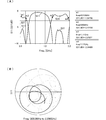
- FIG. 1 shows an example of frequency characteristics of a transformer-type impedance conversion circuit as disclosed in Patent Document 1.
- FIG. 1A shows the reflection loss when the antenna side is viewed from the feeding port of the impedance conversion circuit in the frequency range from 700 MHz to 2.3 GHz
- FIG. 1B shows the impedance locus on the Smith chart.
- the reflection loss is minimum at about 1.9 GHz, that is, the radiation efficiency from the antenna is maximum, but the reflection loss is large and the radiation efficiency is extremely poor at other frequencies, for example, 800 MHz band. Therefore, it cannot be used for the broadband antenna apparatus as described above.
- an antenna device corresponding to a wide frequency band an antenna device having a broadband matching circuit composed of an LC parallel resonance circuit or an LC series resonance circuit is generally used.
- a broadband matching circuit composed of an LC parallel resonance circuit or an LC series resonance circuit is generally used.
- insertion loss occurs to some extent, and signal energy loss occurs.
- the characteristics of the impedance conversion circuit change depending on the arrangement position of the ground plate, the casing, and other components in the vicinity (especially high-frequency components such as an antenna and a strip line).
- An object of the present invention is to solve the above-described problems and provide a front-end circuit that matches a high-frequency circuit and an antenna with a low insertion loss over a wide frequency band, and a communication terminal device including the front-end circuit. It is said.
- the front end circuit includes a power supply side common port to which a high frequency signal in a first frequency band and a high frequency signal in a second frequency band lower than the first frequency band are input or output, a first frequency A first port for inputting or outputting a high-frequency signal in the band and a second port for inputting or outputting a high-frequency signal in the second frequency band, the high-frequency signal in the first frequency band and the high-frequency signal in the second frequency band
- a front end circuit including a power supply side frequency selective circuit for performing demultiplexing or multiplexing with A first impedance conversion circuit including a first transformer provided between the first port and the antenna port and in which a primary coil and a secondary coil are electromagnetically coupled, or the second port and the antenna port (the antenna And a second impedance conversion circuit including a second transformer in which a primary side coil and a secondary side coil are electromagnetically coupled to each other.
- the front end circuit has a common port on the antenna side to which a high frequency signal in the first frequency band and a high frequency signal in the second frequency band are input or output, and a high frequency signal in the first frequency band is input or output. And an antenna for performing demultiplexing or combining of the high frequency signal of the first frequency band and the high frequency signal of the second frequency band.
- a first impedance conversion circuit including a first transformer connected between the first port and the power supply port and in which a primary coil and a secondary coil are electromagnetically coupled, or the second port and a power supply circuit (the power supply) And at least one of a second impedance conversion circuit including a second transformer in which a primary side coil and a secondary side coil are electromagnetically coupled to each other.
- a communication terminal device includes a power supply side common port to which a high frequency signal in a first frequency band and a high frequency signal in a second frequency band lower than the first frequency band are input or output, a first frequency A first port for inputting or outputting a high-frequency signal in the band and a second port for inputting or outputting a high-frequency signal in the second frequency band, the high-frequency signal in the first frequency band and the high-frequency signal in the second frequency band
- a front-end circuit having a power-feed-side frequency selective circuit that performs demultiplexing or multiplexing with
- a high-frequency circuit including a
- the antenna side common port to which the high frequency signal of the first frequency band and the high frequency signal of the second frequency band are input or output, and the high frequency signal of the first frequency band is input or output.
- a first impedance conversion circuit including an antenna-side frequency selective circuit and a first transformer connected between the first port and the power feeding port and having a primary side coil and a secondary side coil electromagnetically coupled;
- a second input including a second transformer connected between the two ports and a power feeding circuit (a power feeding circuit different from the power feeding circuit or the power feeding circuit) and having a primary coil and a secondary coil electromagnetically coupled.
- a front end circuit having at least one-impedance converting circuit, A high frequency circuit connected to the first impedance conversion circuit and a high frequency circuit connected to the second impedance conversion circuit are provided.
- a front-end circuit that matches a high-frequency circuit and an antenna with a simple circuit configuration and low insertion loss over a wide frequency band, and a communication terminal device including the front-end circuit.
- FIG. 1A shows the reflection loss when the antenna side is viewed from the power feeding port of the transformer-type impedance conversion circuit as shown in Patent Document 1
- FIG. 1B shows the impedance locus on the Smith chart.
- FIG. 2 is a circuit diagram of a main part of a front end circuit and a communication terminal apparatus including the front end circuit according to the first embodiment.
- FIG. 3A is a characteristic diagram of reflection loss and passage loss of the front end circuit 301 according to the first embodiment when the antenna side is viewed from the power supply side common port Pin
- FIG. 3B is a Smith chart of reflection loss. This is the upper impedance locus.
- FIG. 4 is a circuit diagram of a main part of a front end circuit and a communication terminal device having the same according to the second embodiment.
- FIG. 5 is a circuit diagram of a main part of another front-end circuit and a communication terminal apparatus including the front-end circuit according to the second embodiment.
- FIG. 6A is a circuit diagram of a main part of a front end circuit and a communication terminal apparatus having the same according to the third embodiment.
- FIG. 6B is a circuit diagram of a main part of another front end circuit of the third embodiment and a communication terminal device including the front end circuit.
- FIG. 7 is a circuit diagram of still another front end circuit according to the third embodiment and a main part of a communication terminal device including the front end circuit.
- FIG. 8 is a circuit diagram of a main part of a front end circuit and a communication terminal apparatus having the same according to the fourth embodiment.
- FIG. 6A is a circuit diagram of a main part of a front end circuit and a communication terminal apparatus having the same according to the third embodiment.
- FIG. 6B is a circuit diagram of a main part of another front end circuit of the third embodiment and a communication terminal device including
- FIG. 9 is a circuit diagram of a main part of another front end circuit and a communication terminal apparatus including the front end circuit according to the fourth embodiment.
- FIG. 10 is a circuit diagram of a main part of a front end circuit and a communication terminal apparatus having the same according to the fifth embodiment.
- FIG. 11 is a circuit diagram of a main part of a front end circuit and a communication terminal apparatus having the same according to the sixth embodiment.
- 12A is an equivalent circuit diagram of the impedance conversion circuits 206A and 206B in FIG. 11, and
- FIG. 12B is an equivalent circuit diagram of the antenna 11.
- FIG. 13 is a circuit diagram of a main part of a front end circuit and a communication terminal apparatus having the same according to the seventh embodiment.
- FIG. 13 is a circuit diagram of a main part of a front end circuit and a communication terminal apparatus having the same according to the seventh embodiment.
- FIG. 14 is a diagram showing the relationship between the current flowing through the impedance conversion circuits 207A and 207B and the direction of the magnetic flux.
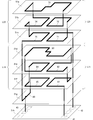
- FIG. 15 is a diagram illustrating an example of a conductor pattern of each layer of the impedance conversion circuit according to the eighth embodiment configured on a multilayer substrate.
- FIG. 16 shows the main magnetic flux passing through the coil element by the conductor pattern formed in each layer of the multilayer substrate shown in FIG.
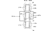
- FIG. 17 is a circuit diagram of an impedance conversion circuit according to the ninth embodiment.
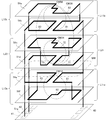
- FIG. 18 is a diagram illustrating an example of a conductor pattern of each layer when the impedance conversion circuit according to the ninth embodiment is configured on a multilayer substrate.
- FIG. 19 is a circuit diagram of an impedance conversion circuit according to the tenth embodiment.
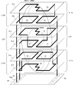
- FIG. 20 is a diagram illustrating an example of a conductor pattern of each layer when the impedance conversion circuit according to the tenth embodiment is configured on a multilayer substrate.
- FIG. 21 is a circuit diagram of an impedance conversion circuit according to the eleventh embodiment.
- FIG. 22 is a diagram illustrating an example of a conductor pattern of each layer when the impedance conversion circuit according to the eleventh embodiment is configured on a multilayer substrate.
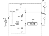
- FIG. 2 is a circuit diagram of a main part of a front end circuit and a communication terminal apparatus including the front end circuit according to the first embodiment.
- the front end circuit 301 of the first embodiment has a power supply side common port Pin and an antenna port Pout, the high frequency circuit 30 is connected to the power supply side common port Pin, and the antenna (radiating element) 11 is connected to the antenna port Pout.
- the front end circuit 301 includes a power supply side frequency selectivity circuit (hereinafter, “diplexer”) 101 and an impedance conversion circuit 201.
- diplexer power supply side frequency selectivity circuit
- the diplexer 101 includes a high frequency signal in a 2 GHz band (hereinafter, “high band”) that is a first frequency band, and a high frequency in an 800 MHz band (hereinafter, “low band”) that is a second frequency band that is lower than the first frequency band.
- high band a high frequency signal in a 2 GHz band
- low band a high frequency in an 800 MHz band
- the impedance conversion circuit 201 is connected between the second port P2 of the diplexer 101 and the antenna port Pout.
- the first port P1 of the diplexer 101 is directly connected to the antenna port Pout via the transmission line TL.
- the impedance conversion circuit 201 includes a first circuit (primary circuit) including a first coil element L1, a second circuit (2) including a second coil element L2 and a third coil element L3 connected in series to the second coil. Secondary circuit).
- the first coil element L1 corresponds to a primary coil described in the claims
- the second coil element L2 and the third coil element L3 correspond to a secondary coil described in the claims.
- the first coil element L1 and the second coil element L2 are electromagnetically coupled in opposite phases
- the first coil element L1 and the third coil element L3 are electromagnetically coupled in opposite phases.
- the first coil element L1, the second coil element L2, and the third coil element L3 are arranged so that their winding axes are substantially the same straight line, and between the second coil element L2 and the third coil element L3. It arrange
- the impedance conversion circuit 201 constitutes a transformer type impedance conversion circuit.
- the diplexer 101 demultiplexes / combines the high-band high-frequency signal and the low-band high-frequency signal.
- the low-band high-frequency signal propagates through the impedance conversion circuit 201, and the high-band high-frequency signal propagates through the transmission line TL.
- the length of the housing is less than 1 ⁇ 4 wavelength, and thus tends to be low impedance.
- an impedance comparable to that of a monopole antenna can be obtained. For example, it is 25 ⁇ for the high band and about 8 ⁇ for the low band.
- the impedance conversion ratio of the impedance conversion circuit 201 is about 50: 8. Therefore, the impedance conversion circuit 201 normally matches the impedance of the low-band high-frequency signal. Since the high-band high-frequency signal does not pass through the impedance conversion circuit 201, the impedance does not become too high, and the high-frequency signal is matched to the extent that no problem in use occurs.
- FIG. 3 shows an example of the frequency characteristic of the front end circuit 301 according to the first embodiment.
- FIG. 3A is a characteristic diagram of pass loss and reflection loss when the antenna side is viewed from the power supply side common port Pin of the front end circuit 301 in the frequency range from 800 MHz to 2.2 GHz.
- S11 represents a reflection loss
- S21 represents a passage loss.
- FIG. 3B is an impedance locus on the Smith chart of reflection loss.
- the characteristic of the low band (for example, 820 MHz band) is the characteristic through the impedance conversion circuit 201 of the front end circuit 301.
- the output impedance of the impedance conversion circuit 201 is matched with the 101 input impedance of the diplexer.
- the antenna-side impedance of the high-pass filter portion of the diplexer 101 is matched with the characteristic impedance of the antenna.
- FIG. 4 is a circuit diagram of a main part of a front end circuit and a communication terminal device having the same according to the second embodiment.
- FIG. 5 is a circuit diagram of the main part of another front-end circuit according to the second embodiment and a communication terminal apparatus including the front-end circuit.
- the front end circuit is composed of a diplexer 102A and an impedance conversion circuit 202.
- the diplexer 102A includes a high-pass filter that includes a capacitor DC11 and an inductor DL11, and a low-pass filter that includes an inductor DL21 and a capacitor DC21.
- the diplexer 102A includes a power supply-side common port Pin that inputs and outputs a high-band high-frequency signal and a low-band high-frequency signal, a first port P1 that inputs and outputs a high-band high-frequency signal, and a second port that inputs and outputs a low-band high-frequency signal.
- a port P2 is provided to multiplex and demultiplex a low-band high-frequency signal and a high-band high-frequency signal.
- the configuration of the transformer part of the impedance conversion circuit 202 is the same as that shown in the first embodiment, but in the example of FIG. 4, it is integrated including the transmission line TL.
- the first coil element L1, the second coil element L2, and the third coil element L3 of the impedance conversion circuit 202 are integrally configured on a multilayer substrate that is a laminate of a plurality of dielectric layers or magnetic layers. At least a coupling region between the first coil element L1 and the second coil element L2 and a coupling region between the first coil element L1 and the third coil element L3 are located in the multilayer substrate.
- capacitors DC11 and DC21 and the inductors DL11 and DL21 of the diplexer 102A may have chip parts mounted on the surface of the multilayer substrate, respectively, or may be integrally formed inside the multilayer substrate with a conductor pattern. In either case, a modularized front-end circuit can be configured.
- the front end circuit includes a diplexer 102 ⁇ / b> B and an impedance conversion circuit 202.
- the diplexer 102B includes a high-pass filter that includes a capacitor DC11 and an inductor DL11, and a low-pass filter that includes an inductor DL21 and a capacitor DC21.
- the difference from the diplexer 102A in FIG. 4 is the connection relationship between the capacitor and the inductor.
- FIG. 4 shows a circuit when the impedance of the first port P1 is higher than that of the power supply side common port Pin in the high band and the impedance of the second port P2 is lower than that of the power supply side common port Pin in the low band.
- FIG. 5 is a circuit in the case where the impedance of the first port P1 is lower than that of the power supply side common port Pin in the high band and the impedance of the second port P2 is higher than that of the power supply side common port Pin in the low band.
- FIG. 6A is a circuit diagram of a main part of a front end circuit and a communication terminal device including the same according to the third embodiment
- FIG. 6B is another front end circuit according to the third embodiment and a communication terminal device including the same. It is a circuit diagram of the principal part.
- FIG. 7 is a circuit diagram of still another front end circuit according to the third embodiment and a main part of a communication terminal apparatus including the front end circuit.
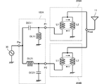
- the front-end circuit 303A includes a diplexer 102A, a first impedance conversion circuit 203A, and a second impedance conversion circuit 203B.
- a first impedance conversion circuit 203A is connected to the first port P1 of the diplexer 102A, and a second impedance conversion circuit 203B is connected to the second port P2 of the diplexer 102A.
- the high-band high-frequency signal is input / output through the port P1 of the diplexer 102A, it passes through the first impedance conversion circuit 203A. Since the low-band high-frequency signal is input / output through the port P2 of the diplexer 102A, it passes through the second impedance conversion circuit 203B.
- the impedance conversion ratio of the first impedance conversion circuit 203A is determined so as to match the impedance of the antenna 11 in the high band.
- the impedance conversion ratio of the second impedance conversion circuit 203B is determined so as to match the impedance of the antenna 11 in the low band. For example, if the impedance of the antenna 11 is 25 ⁇ in the high band and about 8 ⁇ in the low band, and the impedance of the high frequency circuit 30 is 50 ⁇ , the impedance conversion ratio of the impedance conversion circuit 203A is about 50:25, and the impedance conversion of the impedance conversion circuit 203B. The ratio is about 50: 8.
- the impedance conversion ratio of the low band impedance conversion circuit Is larger than the impedance conversion ratio of the high-band impedance conversion circuit.
- the front end circuit 303B includes a diplexer 102A and an impedance conversion circuit 203B. Unlike the front-end circuit of FIG. 6A and the communication terminal device including the front-end circuit, the high-band impedance conversion circuit 203A is not provided, the low-band impedance conversion circuit 203B is provided, the high-band antenna port Pout_H and the low-band impedance conversion circuit 203B are provided. Antenna port Pout_L is provided separately.
- the impedance conversion circuit 203B may be provided only in the low-band high-frequency circuit.
- a high-band antenna port Pout_H and a low-band antenna port Pout_L may be provided separately to connect the high-band antenna 11H and the low-band antenna 11L.
- FIG. 7 is composed of a diplexer 102B and impedance conversion circuits 203A and 203B. Only the configuration of the diplexer is different, and the basic functions and effects are the same as those shown in FIG. 6A.
- FIG. 8 is a circuit diagram of a main part of a front end circuit and a communication terminal apparatus having the same according to the fourth embodiment.
- FIG. 9 is a circuit diagram of a main part of another front-end circuit according to the fourth embodiment and a communication terminal device including the front-end circuit.
- a front end circuit is configured by the diplexer 102A, the impedance conversion circuits 203A and 203B, and the antenna-side frequency selectivity circuit (hereinafter, “diplexer”) 104A.
- a first impedance conversion circuit 203A is connected to the first port Pf1 of the diplexer 102A on the power supply side, and a second impedance conversion circuit 203B is connected to the second port Pf2 of the diplexer 102A.
- the antenna-side diplexer 104A includes a high-pass filter including a capacitor DC12 and an inductor DL12, and a low-pass filter including an inductor DL22 and a capacitor DC22.
- the antenna-side diplexer 104A includes an antenna-side common port Pout, a first port Pa1 through which a high-band high-frequency signal is input / output, and a second port Pa2 through which a low-band high-frequency signal is input / output. Also, demultiplexing or multiplexing of low-band high-frequency signals.
- the antenna-side diplexer 104B is configured by a capacitor DC12 and an inductor DL22.
- the basic functions and effects are the same as those shown in FIG. In this way, a diplexer may be provided also on the antenna side.
- FIG. 10 is a circuit diagram of a main part of a front end circuit and a communication terminal apparatus having the same according to the fifth embodiment.
- the impedance conversion circuits 203A and 203B and the antenna-side diplexer 104A constitute a front-end circuit.
- the antenna-side diplexer 104A includes an antenna-side common port Pout, a first port Pa1 through which a high-band high-frequency signal is input / output, and a second port Pa2 through which a low-band high-frequency signal is input / output. Splits or multiplexes low-band high-frequency signals.
- a high-band first impedance conversion circuit 203A is connected between the first port Pa1 and the first power supply port Pin1.
- a low-band second impedance conversion circuit 203B is connected between the second port Pa2 and the second power feeding port Pin2.
- a high-band high-frequency circuit 30A is connected to the first power supply port Pin1.
- a low-band high-frequency circuit 30B is connected to the second power supply port Pin2.
- the antenna 11 is connected to the antenna side common port Pout.
- the first impedance conversion circuit 203A includes a first transformer in which a primary coil and a secondary coil are electromagnetically coupled.
- the second impedance conversion circuit 203B includes a second transformer in which a primary coil and a secondary coil are electromagnetically coupled.
- the impedance conversion ratio of the first impedance conversion circuit 203A is determined so as to match the impedance of the antenna 11 in the high band.
- the impedance conversion ratio of the second impedance conversion circuit 203B is determined so as to match the impedance of the antenna 11 in the low band. In this way, a diplexer may be provided only on the antenna side.
- the first impedance conversion circuit 203A and the second impedance conversion circuit 203B may be provided.
- the antenna 11 and the high-frequency circuit 30A are matched in such a high band that there is no problem in using the return loss, the high-band first impedance conversion circuit 203A is not provided, and the low-band first impedance conversion circuit 203A is not provided. Only two impedance conversion circuits 203B may be provided.
- FIG. 11 is a circuit diagram of a main part of a front end circuit and a communication terminal apparatus having the same according to the sixth embodiment.
- the impedance conversion circuits 206A and 206B and the power supply side diplexer 102A constitute a front end circuit.
- Impedance conversion circuits 206A and 206B each have a first coil element L1 and a second coil element L2.
- the first coil element L1 corresponds to a primary coil described in the claims
- the second coil element L2 corresponds to a secondary coil described in the claims.
- the first coil element L1 and the second coil element L2 are arranged to form a closed magnetic circuit.
- the first coil element L1 and the second coil element L2 are connected such that the first coil element L1 and the second coil element L2 are electromagnetically coupled in opposite phases.
- first coil element L1 and the second coil element L2 are integrally formed on a multilayer substrate that is a laminate of a plurality of dielectric layers or magnetic layers, and the first coil element L1 and the second coil element The coupling region of L2 is located in the multilayer substrate.
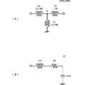
- FIG. 12A is an equivalent circuit diagram of the impedance conversion circuits 206A and 206B in FIG. 11, and FIG. 12B is an equivalent circuit diagram of the antenna 11.
- Each of the impedance conversion circuits 206A and 206B can be equivalently converted to a T-type circuit including three inductance elements La, Lb, and Lc as shown in FIG. That is, the T-type circuit includes a first inductance element La connected between the power supply side port and the branch point A, a second inductance element Lb connected between the antenna side port and the branch point A, And a third inductance element Lc connected between the ground port and the branch point A.
- the antenna 11 is composed of an inductance component LANT, a radiation resistance component Rr, and a capacitance component CANT generated between the radiation element and the ground.
- the first coil element L1 and the second coil element L2 are coupled to each other to generate a mutual inductance M.
- the function realized by the first coil element L1 and the second coil element L2 is by first performing impedance conversion so as to match the real part of the impedance on the power feeding circuit side (high frequency circuit side) with the real part of the impedance on the antenna side. is there.
- the impedance on the power feeding circuit side is set to 50 ⁇ , but the impedance of the antenna 11 is often lower than 50 ⁇ .
- the impedance conversion ratio of the impedance conversion circuit is (L1 + L2 + 2M): L2.
- the radiation resistance Rr of the antenna 11 is matched with the impedance (50 ⁇ ) of the high-frequency circuit on the power feeding side. That is, the impedance conversion ratio of the impedance conversion circuit 206A shown in FIG. 11 is determined so as to match the real part of the impedance of the antenna 11 in the high band.
- the impedance conversion circuit 206B has an impedance conversion ratio determined so as to match the real part of the impedance of the antenna 11 in the low band.
- the inductance component LANT of the antenna 11 alone acts so as to be canceled by the negative inductance component ( ⁇ M) in the impedance conversion circuits 206A and 206B. That is, the inductance component (of the antenna 11 including the second inductance element Lb) viewed from the point A in FIG. 12A is small (ideally zero), and as a result, The impedance frequency characteristic of this antenna becomes small.
- the mutual inductance M is determined so that the inductance component of the antenna 11 in the high band is canceled.
- the impedance conversion circuit 206B has a mutual inductance M determined so that the inductance component of the antenna 11 in the low band is canceled out.
- FIG. 13 is a circuit diagram of a main part of a front end circuit and a communication terminal apparatus having the same according to the seventh embodiment.
- the impedance conversion circuit is different from the front end circuit shown in FIG.
- the impedance conversion circuit 207A includes a first coil L1 and a second coil L2, as shown in FIG.
- the first coil L1 includes two coil elements L11 and L12 connected in series.
- the second coil L2 is composed of two coil elements L21 and L22 connected in series.
- the impedance conversion circuit 207B includes a first coil L1 and a second coil L2.
- the first coil L1 is composed of two coil elements L11 and L12 connected in series
- the second coil L2 is composed of two coil elements L21 and L22 connected in series.
- FIG. 14 is a diagram showing the relationship between the current flowing through the impedance conversion circuits 207A and 207B and the direction of the magnetic flux.
- the current is represented by solid arrows and the magnetic flux is represented by broken arrows.
- the coil elements L11 and L12 connected in series constitute a closed magnetic circuit
- the coil elements L21 and L22 connected in series constitute a closed magnetic circuit
- the coil elements L11 and L21 constitute a closed magnetic circuit
- the coil elements L12 and L22 also constitute a closed magnetic circuit.
- the entire coil elements L11, L21, L22, and L12 also constitute a closed magnetic circuit.
- FIG. 15 is a diagram illustrating an example of a conductor pattern of each layer of the impedance conversion circuit according to the eighth embodiment configured on a multilayer substrate. Each layer is composed of a magnetic sheet.
- This impedance conversion circuit is a high-band or low-band impedance conversion circuit.
- conductor patterns 73 are formed on the first layer 51a
- conductor patterns 72 and 74 are formed on the second layer 51b
- conductor patterns 71 and 75 are formed on the third layer 51c.
- Conductor patterns 63 are formed on the fourth layer 51d
- conductor patterns 62 and 64 are formed on the fifth layer 51e
- conductor patterns 61 and 65 are formed on the sixth layer 51f.
- a conductor pattern 66 is formed on the seventh layer 51g.
- a power supply terminal 41, a ground terminal 42, and an antenna terminal 43 are formed in the eighth layer 51h.
- a broken line extending in the vertical direction in FIG. 15 is a via conductor, and the conductor patterns are connected between the layers.
- the right half of the conductor pattern 63 and the conductor patterns 61 and 62 constitute a first coil element L11. Further, the left half of the conductor pattern 63 and the conductor patterns 64 and 65 constitute a second coil element L12. Further, the right half of the conductor pattern 73 and the conductor patterns 71 and 72 constitute a third coil element L21. The left half of the conductor pattern 73 and the conductor patterns 74 and 75 constitute a fourth coil element L22.
- the winding axis of each of the coil elements L11 to L22 is oriented in the stacking direction of the multilayer substrate. And the winding axis of the 1st coil element L11 and the 2nd coil element L12 is juxtaposed in a different relationship.
- the third coil element L21 and the fourth coil element L22 are juxtaposed with each other with different winding axes. Then, the respective winding ranges of the first coil element L11 and the third coil element L21 overlap at least partially in plan view, and the respective winding ranges of the second coil element L12 and the fourth coil element L22. Overlap at least partially in plan view. In this example, they overlap almost completely. In this way, four coil elements are constituted by the conductor pattern of the figure eight structure.
- Each layer may be composed of a dielectric sheet. However, if a magnetic sheet having a high relative permeability is used, the coupling coefficient between the coil elements can be further increased.
- FIG. 16 shows the main magnetic flux passing through the coil element by the conductor pattern formed in each layer of the multilayer substrate shown in FIG.
- the magnetic flux FP12 passes through the first coil element L11 by the conductor patterns 61 to 63 and the second coil element L12 by the conductor patterns 63 to 65. Further, the magnetic flux FP34 passes through the third coil element L21 by the conductor patterns 71 to 73 and the fourth coil element L22 by the conductor patterns 73 to 75. In this way, the coil elements can be tightly coupled.
- FIG. 17 is a circuit diagram of an impedance conversion circuit according to the ninth embodiment.
- This impedance conversion circuit is a high-band or low-band impedance conversion circuit.
- the impedance conversion circuit includes a first series circuit 26 connected between the power supply side port Pf and the antenna side port Pa, and a first series circuit 26 connected between the power supply side port Pf and the antenna side port Pa. 3 series circuit 28 and a second series circuit 27 connected between the port Pa on the antenna side and the ground.
- the first series circuit 26 is a circuit in which a first coil element L11a and a second coil element L12a are connected in series.
- the second series circuit 27 is a circuit in which a third coil element L21 and a fourth coil element L22 are connected in series.
- the third series circuit 28 is a circuit in which a fifth coil element L11b and a sixth coil element L12b are connected in series.
- an elliptical broken line M12 represents a coupling between the coil elements L11a and L12a
- an elliptical broken line M34 represents a coupling between the coil elements L21 and L22
- an elliptical broken line M56 represents a coupling between the coil elements L11b and L12b.
- An elliptical broken line M135 represents coupling of the coil elements L11a, L21, and L11b.
- an elliptical broken line M246 represents coupling of the coil elements L12a, L22, and L12b.
- FIG. 18 is a diagram illustrating an example of a conductor pattern of each layer when the impedance conversion circuit according to the ninth embodiment is configured on a multilayer substrate.
- Each layer is composed of a magnetic sheet.
- the conductor pattern 82 is formed on the first layer 51a
- the conductor patterns 81 and 83 are formed on the second layer 51b
- the conductor pattern 72 is formed on the third layer 51c.
- Conductive patterns 71 and 73 are formed on the fourth layer 51d
- conductive patterns 61 and 63 are formed on the fifth layer 51e
- conductive patterns 62 are formed on the sixth layer 51f.
- a power feeding terminal 41, a ground terminal 42, and an antenna terminal 43 are formed in the seventh layer 51g.
- a broken line extending in the vertical direction in FIG. 18 is a via conductor, and the conductor patterns are connected between the layers.
- the right half of the conductor pattern 62 and the conductor pattern 61 constitute a first coil element L11a. Further, the left half of the conductor pattern 62 and the conductor pattern 63 constitute a second coil element L12a.
- the third coil element L21 is configured by the conductor pattern 71 and the right half of the conductor pattern 72.
- the left half of the conductor pattern 72 and the conductor pattern 73 constitute a fourth coil element L22.
- the fifth coil element L11b is configured by the conductor pattern 81 and the right half of the conductor pattern 82.
- the left half of the conductor pattern 82 and the conductor pattern 83 constitute a sixth coil element L12b.
- the dashed ellipse represents a closed magnetic circuit.
- the closed magnetic circuit CM12 is linked to the coil elements L11a and L12a.
- the closed magnetic circuit CM34 is linked to the coil elements L21 and L22.
- the closed magnetic circuit CM56 is linked to the coil elements L11b and L12b.
- the first coil element L11a and the second coil element L12a constitute the first closed magnetic circuit CM12
- the third coil element L21 and the fourth coil element L22 constitute the second closed magnetic circuit CM34.
- the fifth coil element L11b and the sixth coil element L12b constitute a third closed magnetic circuit CM56.
- the plane of the two-dot chain line is such that the coil elements L11a and L21, L21 and L11b, L12a and L22, and L22 and L12b are coupled in the opposite direction between the three closed magnetic paths.
- two magnetic walls MW that are equivalently generated.
- the two magnetic walls MW confine the magnetic flux in the closed magnetic circuit by the coil elements L11a and L12a, the magnetic flux in the closed magnetic circuit by the coil elements L21 and L22, and the magnetic flux in the closed magnetic circuit by the coil elements L11b and L12b.
- the second closed magnetic circuit CM34 is sandwiched between the first closed magnetic circuit CM12 and the third closed magnetic circuit CM56 in the layer direction.
- the second closed magnetic circuit CM34 is sandwiched between two magnetic walls and sufficiently confined (the confinement effect is enhanced). That is, it can act as a transformer having a very large coupling coefficient.
- the gap between the closed magnetic circuits CM12 and CM34 and between the CM34 and CM56 can be widened to some extent.
- a circuit in which a series circuit including the coil elements L11a and L12a and a series circuit including the coil elements L11b and L12b are connected in parallel is referred to as a primary circuit, and a series circuit including the coil elements L21 and L22 is referred to as a secondary circuit.
- the capacitance generated between each of the three series circuits 28 can be reduced. That is, the capacitance component of the LC resonance circuit that determines the frequency of the self-resonance point can be reduced.
- the self-resonance is achieved.
- the inductance component of the LC resonance circuit that determines the frequency of the point is reduced.
- the capacitance component and inductance component of the LC resonance circuit that determines the frequency of the self-resonance point are reduced, and the frequency of the self-resonance point can be set to a high frequency sufficiently away from the use frequency band. It acts as a transformer.
- FIG. 19 is a circuit diagram of an impedance conversion circuit according to the tenth embodiment.
- This impedance conversion circuit is a high-band or low-band impedance conversion circuit.
- the impedance conversion circuit includes a first series circuit 26 connected between the power supply side port Pf and the antenna side port Pa, and a first series circuit 26 connected between the power supply side port Pf and the antenna side port Pa. 3 series circuit 28 and a second series circuit 27 connected between the port Pa on the antenna side and the ground.
- the first series circuit 26 is a circuit in which a first coil element L11a and a second coil element L12a are connected in series.
- the second series circuit 27 is a circuit in which a third coil element L21 and a fourth coil element L22 are connected in series.
- the third series circuit 28 is a circuit in which a fifth coil element L11b and a sixth coil element L12b are connected in series.
- an elliptical broken line M12 represents a coupling between the coil elements L11a and L12a
- an elliptical broken line M34 represents a coupling between the coil elements L21 and L22
- an elliptical broken line M56 represents a coupling between the coil elements L11b and L12b.
- An elliptical broken line M135 represents coupling of the coil elements L11a, L21, and L11b.
- an elliptical broken line M246 represents coupling of the coil elements L12a, L22, and L12b.
- FIG. 20 is a diagram illustrating an example of a conductor pattern of each layer when the impedance conversion circuit according to the tenth embodiment is configured on a multilayer substrate.
- Each layer is composed of a magnetic sheet, and the conductor pattern of each layer is formed on the magnetic sheet in the direction shown in FIG. 20, but each conductor pattern is represented by a solid line.
- the linear conductor pattern has a predetermined line width, it is represented by a simple solid line here.
- the closed magnetic circuit CM36 is linked to the coil elements L21, L11b, L12b, and L22. Therefore, an equivalent magnetic wall does not occur between the coil elements L21, L22 and L11b, L12b.
- Other configurations are as described in the fifth embodiment.
- the closed magnetic circuits CM12, CM34, and CM56 shown in FIG. 20 and the closed magnetic circuit CM36 are generated, so that the magnetic flux generated by the coil elements L21 and L22 is absorbed by the magnetic flux generated by the coil elements L11b and L12b. .
- the magnetic flux hardly leaks even in the structure of the sixth embodiment, and as a result, it acts as a transformer having a very large coupling coefficient.
- both the capacitance component and the inductance component of the LC resonance circuit that determines the frequency of the self-resonance point are reduced, and the frequency of the self-resonance point can be set to a high frequency sufficiently away from the use frequency band.
- FIG. 21 is a circuit diagram of an impedance conversion circuit according to the eleventh embodiment.
- This impedance conversion circuit is a high-band or low-band impedance conversion circuit.
- the impedance conversion circuit includes a first series circuit 26 connected between the power supply side port Pf and the antenna side port Pa, and a first series circuit 26 connected between the power supply side port Pf and the antenna side port Pa. 3 series circuit 28 and a second series circuit 27 connected between the port Pa on the antenna side and the ground.
- FIG. 22 is a diagram showing an example of a conductor pattern of each layer when the impedance conversion circuit according to the eleventh embodiment is configured on a multilayer substrate.
- Each layer is composed of a magnetic sheet.
- the closed magnetic circuit CM16 is linked to all the coil elements L11a to L12b. Therefore, in this case, an equivalent magnetic wall does not occur.
- Other configurations are as shown in the ninth embodiment and the tenth embodiment.
- the closed magnetic circuits CM12, CM34, and CM56 shown in FIG. 22 and the closed magnetic circuit CM16 are generated, so that the magnetic flux due to the coil elements L11a to L12b is hardly leaked. As a result, the coupling coefficient is large. Can act as a transformer.
- both the capacitance component and the inductance component of the LC resonance circuit that determines the frequency of the self-resonance point are reduced, and the frequency of the self-resonance point can be set to a high frequency sufficiently away from the use frequency band.
- each of the eighth to eleventh embodiments the high-band or low-band impedance conversion circuit has been described.
- each of the high-band and low-band impedance conversion circuits is configured as a single laminate and modularized. May be.
- the present invention includes a form in which, for example, an impedance conversion circuit is provided in a high-band high-frequency circuit, and an impedance conversion circuit is not provided in a low-band high-frequency circuit.
- CANT Capacitance components CM12, CM34, CM56, CM16, CM36 ... Closed magnetic paths FP12, FP34 ... Magnetic flux L1 ... First coil element L2 ... Second coil element L3 ... Third coil element L11 ... First coil element L12 ... Second Coil element L11a, first coil element L12a, second coil element L21, third coil element L22, fourth coil element L11b, fifth coil element L12b, sixth coil element La, Lb, Lc. ... Inductance element LANT ... Inductance component M of antenna ... Mutual inductance MW ... Magnetic wall Pin ... Power supply side common port Pout ... Antenna port / antenna side common port Rr ... Radiation resistance TL ...
Landscapes
- Engineering & Computer Science (AREA)
- Computer Networks & Wireless Communication (AREA)
- Signal Processing (AREA)
- Power Engineering (AREA)
- Transceivers (AREA)
- Details Of Aerials (AREA)
- Transmitters (AREA)
- Input Circuits Of Receivers And Coupling Of Receivers And Audio Equipment (AREA)
Abstract
L'invention concerne un circuit frontal (301) doté d'un diplexeur (101) et d'un circuit de conversion d'impédance (201). Ledit diplexeur (101) comprend : un port commun côté alimentation électrique (Pin) par lequel des signaux de haute fréquence d'une bande élevée et des signaux de haute fréquence d'une bande basse sont injectés et prélevés; un premier port (P1) par lequel des signaux de haute fréquence de la bande élevée sont injectés et prélevés; et un second port (P2) par lequel des signaux de haute fréquence de la bande basse sont injectés et prélevés. Ledit diplexeur (101) multiplexe et démultiplexe lesdits signaux de haute fréquence de la bande basse et lesdits signaux de haute fréquence de la bande élevée. Le circuit de conversion d'impédance (201) est connecté entre le second port (P2) du diplexeur (101) et un port d'antenne (Pout). Le premier port (P1) du diplexeur (101) est connecté directement audit port d'antenne (Pout) via une ligne d'émission.
Priority Applications (3)
| Application Number | Priority Date | Filing Date | Title |
|---|---|---|---|
| JP2013513980A JP5850049B2 (ja) | 2011-05-09 | 2012-04-27 | 通信端末装置 |
| CN201280022414.3A CN103548261B (zh) | 2011-05-09 | 2012-04-27 | 前端电路及通信终端装置 |
| US14/072,818 US9197187B2 (en) | 2011-05-09 | 2013-11-06 | Front-end circuit and communication terminal apparatus |
Applications Claiming Priority (2)
| Application Number | Priority Date | Filing Date | Title |
|---|---|---|---|
| JP2011103970 | 2011-05-09 | ||
| JP2011-103970 | 2011-05-09 |
Related Child Applications (1)
| Application Number | Title | Priority Date | Filing Date |
|---|---|---|---|
| US14/072,818 Continuation US9197187B2 (en) | 2011-05-09 | 2013-11-06 | Front-end circuit and communication terminal apparatus |
Publications (1)
| Publication Number | Publication Date |
|---|---|
| WO2012153654A1 true WO2012153654A1 (fr) | 2012-11-15 |
Family
ID=47139138
Family Applications (1)
| Application Number | Title | Priority Date | Filing Date |
|---|---|---|---|
| PCT/JP2012/061339 Ceased WO2012153654A1 (fr) | 2011-05-09 | 2012-04-27 | Circuit frontal et dispositif terminal de communication |
Country Status (4)
| Country | Link |
|---|---|
| US (1) | US9197187B2 (fr) |
| JP (3) | JP5850049B2 (fr) |
| CN (2) | CN105553438B (fr) |
| WO (1) | WO2012153654A1 (fr) |
Cited By (4)
| Publication number | Priority date | Publication date | Assignee | Title |
|---|---|---|---|---|
| WO2016114182A1 (fr) * | 2015-01-16 | 2016-07-21 | 株式会社村田製作所 | Circuit de mise en correspondance d'antennes, dispositif d'antenne et dispositif de terminal de communication |
| JPWO2015151329A1 (ja) * | 2014-04-01 | 2017-04-13 | 株式会社村田製作所 | アンテナ整合装置 |
| US10432236B2 (en) | 2015-07-03 | 2019-10-01 | Murata Manufacturing Co., Ltd. | Front-end module |
| WO2023032511A1 (fr) * | 2021-09-03 | 2023-03-09 | 株式会社村田製作所 | Dispositif d'antenne et dispositif de terminal de communication |
Families Citing this family (10)
| Publication number | Priority date | Publication date | Assignee | Title |
|---|---|---|---|---|
| JPWO2012153691A1 (ja) * | 2011-05-09 | 2014-07-31 | 株式会社村田製作所 | インピーダンス変換回路および通信端末装置 |
| US10535921B2 (en) | 2014-09-05 | 2020-01-14 | Smart Antenna Technologies Ltd. | Reconfigurable multi-band antenna with four to ten ports |
| GB2529884B (en) * | 2014-09-05 | 2017-09-13 | Smart Antenna Tech Ltd | Reconfigurable multi-band antenna with independent control |
| CN104617907B (zh) * | 2015-03-02 | 2018-08-10 | 联想(北京)有限公司 | 一种双工器及电子设备 |
| WO2016194470A1 (fr) * | 2015-06-01 | 2016-12-08 | 株式会社村田製作所 | Circuit frontal, circuit d'antenne et dispositif de communication |
| CN105140644A (zh) * | 2015-08-24 | 2015-12-09 | 联想(北京)有限公司 | 一种天线及电子设备 |
| WO2017111910A1 (fr) | 2015-12-21 | 2017-06-29 | Intel Corporation | Composants passifs rf intégrés à hautes performances utilisant un procédé lithographique double |
| KR101991219B1 (ko) * | 2016-05-19 | 2019-06-19 | 가부시키가이샤 무라타 세이사쿠쇼 | 필터 장치 |
| EP3767742B1 (fr) * | 2018-05-08 | 2023-11-22 | Huawei Technologies Co., Ltd. | Dispositif d'antenne et terminal mobile |
| WO2025134482A1 (fr) * | 2023-12-20 | 2025-06-26 | 株式会社村田製作所 | Dispositif d'antenne et dispositif de terminal de communication |
Citations (7)
| Publication number | Priority date | Publication date | Assignee | Title |
|---|---|---|---|---|
| JPH02261209A (ja) * | 1989-03-31 | 1990-10-24 | Japan Radio Co Ltd | 自動整合方法 |
| JPH0380509A (ja) * | 1989-08-23 | 1991-04-05 | Murata Mfg Co Ltd | 積層トランス |
| JP2003100518A (ja) * | 2001-09-21 | 2003-04-04 | Hitachi Media Electoronics Co Ltd | 整合器 |
| JP2007288361A (ja) * | 2006-04-13 | 2007-11-01 | Toshiba Corp | 不平衡給電アンテナ装置 |
| JP2012084833A (ja) * | 2010-01-19 | 2012-04-26 | Murata Mfg Co Ltd | 高周波トランス、電子回路および電子機器 |
| JP2012085250A (ja) * | 2010-08-11 | 2012-04-26 | Murata Mfg Co Ltd | 周波数安定化回路、アンテナ装置及び通信端末機器 |
| JP2012085305A (ja) * | 2010-01-19 | 2012-04-26 | Murata Mfg Co Ltd | アンテナ装置および通信端末装置 |
Family Cites Families (16)
| Publication number | Priority date | Publication date | Assignee | Title |
|---|---|---|---|---|
| US3217275A (en) * | 1962-06-01 | 1965-11-09 | Collins Radio Co | Multicoupler system utilizing tunable trap |
| JPS54183246U (fr) * | 1978-06-15 | 1979-12-26 | ||
| WO1999041843A2 (fr) * | 1998-02-17 | 1999-08-19 | Koninklijke Philips Electronics N.V. | Station emettrice/receptrice possedant des moyens recepteurs a impedance equilibree, destines a des signaux de reponse de repeteur |
| JP2000151446A (ja) * | 1998-11-10 | 2000-05-30 | Kokusai Electric Co Ltd | アンテナ装置 |
| JP2002261209A (ja) * | 2001-03-02 | 2002-09-13 | Fujikura Ltd | ファン付きヒートシンク |
| JP2004072445A (ja) | 2002-08-07 | 2004-03-04 | Nippon Hoso Kyokai <Nhk> | 中波放送用アンテナ給電回路 |
| EP1583254B1 (fr) * | 2004-03-30 | 2009-06-17 | TDK Corporation | Diplexeur et circuit d'adapation |
| EP2040377B1 (fr) * | 2006-07-03 | 2018-09-12 | Hitachi Metals, Ltd. | Circuit en dérivation, circuit haute fréquence et module haute fréquence |
| KR100956297B1 (ko) * | 2006-07-05 | 2010-05-10 | 가부시키가이샤 무라타 세이사쿠쇼 | 필터 모듈 및 통신 장치 |
| JP4645603B2 (ja) * | 2007-02-22 | 2011-03-09 | 株式会社村田製作所 | アンテナ構造およびそれを備えた無線通信装置 |
| US7917096B2 (en) * | 2007-03-30 | 2011-03-29 | Sony Ericsson Mobile Communications Ab | Antenna interface circuits including multiple impedance matching networks that are respectively associated with multiple frequency bands and electronic devices incorporating the same |
| WO2009020025A1 (fr) * | 2007-08-09 | 2009-02-12 | Murata Manufacturing Co., Ltd. | Transformateur constitué d'un empilement, convertisseur d'impédance, distributeur égal, procédé de conversion d'impédance et procédé de distribution égale |
| JP4561796B2 (ja) * | 2007-08-31 | 2010-10-13 | ソニー株式会社 | 受電装置、および電力伝送システム |
| KR100986049B1 (ko) * | 2008-08-11 | 2010-10-07 | 주식회사 에이스테크놀로지 | 다중 방송 수신용 모듈형 액티브 안테나 |
| JP5262413B2 (ja) * | 2008-08-12 | 2013-08-14 | 株式会社村田製作所 | マルチバンドデュプレクサモジュール |
| JP2011055258A (ja) * | 2009-09-02 | 2011-03-17 | Murata Mfg Co Ltd | アンテナ装置 |
-
2012
- 2012-04-27 WO PCT/JP2012/061339 patent/WO2012153654A1/fr not_active Ceased
- 2012-04-27 JP JP2013513980A patent/JP5850049B2/ja not_active Expired - Fee Related
- 2012-04-27 CN CN201610027078.1A patent/CN105553438B/zh not_active Expired - Fee Related
- 2012-04-27 CN CN201280022414.3A patent/CN103548261B/zh not_active Expired - Fee Related
-
2013
- 2013-11-06 US US14/072,818 patent/US9197187B2/en active Active
-
2015
- 2015-12-04 JP JP2015237094A patent/JP6194943B2/ja active Active
-
2017
- 2017-06-26 JP JP2017123880A patent/JP6558398B2/ja not_active Expired - Fee Related
Patent Citations (7)
| Publication number | Priority date | Publication date | Assignee | Title |
|---|---|---|---|---|
| JPH02261209A (ja) * | 1989-03-31 | 1990-10-24 | Japan Radio Co Ltd | 自動整合方法 |
| JPH0380509A (ja) * | 1989-08-23 | 1991-04-05 | Murata Mfg Co Ltd | 積層トランス |
| JP2003100518A (ja) * | 2001-09-21 | 2003-04-04 | Hitachi Media Electoronics Co Ltd | 整合器 |
| JP2007288361A (ja) * | 2006-04-13 | 2007-11-01 | Toshiba Corp | 不平衡給電アンテナ装置 |
| JP2012084833A (ja) * | 2010-01-19 | 2012-04-26 | Murata Mfg Co Ltd | 高周波トランス、電子回路および電子機器 |
| JP2012085305A (ja) * | 2010-01-19 | 2012-04-26 | Murata Mfg Co Ltd | アンテナ装置および通信端末装置 |
| JP2012085250A (ja) * | 2010-08-11 | 2012-04-26 | Murata Mfg Co Ltd | 周波数安定化回路、アンテナ装置及び通信端末機器 |
Cited By (9)
| Publication number | Priority date | Publication date | Assignee | Title |
|---|---|---|---|---|
| JPWO2015151329A1 (ja) * | 2014-04-01 | 2017-04-13 | 株式会社村田製作所 | アンテナ整合装置 |
| WO2016114182A1 (fr) * | 2015-01-16 | 2016-07-21 | 株式会社村田製作所 | Circuit de mise en correspondance d'antennes, dispositif d'antenne et dispositif de terminal de communication |
| US10340877B2 (en) | 2015-01-16 | 2019-07-02 | Murata Manufacturing Co., Ltd. | Antenna matching circuit, antenna device, and communication terminal apparatus |
| JP2020014232A (ja) * | 2015-01-16 | 2020-01-23 | 株式会社村田製作所 | アンテナ装置および通信端末装置 |
| US10432236B2 (en) | 2015-07-03 | 2019-10-01 | Murata Manufacturing Co., Ltd. | Front-end module |
| WO2023032511A1 (fr) * | 2021-09-03 | 2023-03-09 | 株式会社村田製作所 | Dispositif d'antenne et dispositif de terminal de communication |
| JPWO2023032511A1 (fr) * | 2021-09-03 | 2023-03-09 | ||
| JP7568122B2 (ja) | 2021-09-03 | 2024-10-16 | 株式会社村田製作所 | アンテナ装置、および通信端末装置 |
| US12407090B2 (en) | 2021-09-03 | 2025-09-02 | Murata Manufacturing Co., Ltd. | Antenna device and communication terminal device |
Also Published As
| Publication number | Publication date |
|---|---|
| CN103548261B (zh) | 2016-02-10 |
| JPWO2012153654A1 (ja) | 2014-07-31 |
| JP6194943B2 (ja) | 2017-09-13 |
| JP6558398B2 (ja) | 2019-08-14 |
| JP2017201805A (ja) | 2017-11-09 |
| CN105553438A (zh) | 2016-05-04 |
| CN103548261A (zh) | 2014-01-29 |
| JP5850049B2 (ja) | 2016-02-03 |
| US20140055209A1 (en) | 2014-02-27 |
| CN105553438B (zh) | 2019-02-12 |
| US9197187B2 (en) | 2015-11-24 |
| JP2016076964A (ja) | 2016-05-12 |
Similar Documents
| Publication | Publication Date | Title |
|---|---|---|
| JP6558398B2 (ja) | 通信端末装置 | |
| CN102341957B (zh) | 天线装置及通信终端装置 | |
| US9106313B2 (en) | Impedance conversion circuit and communication terminal apparatus | |
| JP5477512B2 (ja) | インピーダンス変換回路および通信端末装置 | |
| US9019168B2 (en) | Frequency stabilization circuit, frequency stabilization device, antenna apparatus and communication terminal equipment, and impedance conversion element | |
| JP4935955B2 (ja) | アンテナ装置および通信端末装置 | |
| CN103348531B (zh) | 稳频电路、天线装置及通信终端装置 | |
| JP5957816B2 (ja) | インピーダンス変換デバイス、アンテナ装置および通信端末装置 | |
| JP4389210B2 (ja) | 高周波スイッチ回路 | |
| JP5803190B2 (ja) | アンテナ装置および通信端末装置 |
Legal Events
| Date | Code | Title | Description |
|---|---|---|---|
| 121 | Ep: the epo has been informed by wipo that ep was designated in this application |
Ref document number: 12781994 Country of ref document: EP Kind code of ref document: A1 |
|
| ENP | Entry into the national phase |
Ref document number: 2013513980 Country of ref document: JP Kind code of ref document: A |
|
| NENP | Non-entry into the national phase |
Ref country code: DE |
|
| 122 | Ep: pct application non-entry in european phase |
Ref document number: 12781994 Country of ref document: EP Kind code of ref document: A1 |