WO2012157011A1 - Dispositif de transmission d'énergie et système de transfert d'énergie - Google Patents
Dispositif de transmission d'énergie et système de transfert d'énergie Download PDFInfo
- Publication number
- WO2012157011A1 WO2012157011A1 PCT/JP2011/002663 JP2011002663W WO2012157011A1 WO 2012157011 A1 WO2012157011 A1 WO 2012157011A1 JP 2011002663 W JP2011002663 W JP 2011002663W WO 2012157011 A1 WO2012157011 A1 WO 2012157011A1
- Authority
- WO
- WIPO (PCT)
- Prior art keywords
- power transmission
- transmission device
- power
- device side
- electrode
- Prior art date
- Legal status (The legal status is an assumption and is not a legal conclusion. Google has not performed a legal analysis and makes no representation as to the accuracy of the status listed.)
- Ceased
Links
Images



Classifications
-
- H—ELECTRICITY
- H02—GENERATION; CONVERSION OR DISTRIBUTION OF ELECTRIC POWER
- H02J—ELECTRIC POWER NETWORKS; CIRCUIT ARRANGEMENTS OR SYSTEMS FOR SUPPLYING OR DISTRIBUTING ELECTRIC POWER; SYSTEMS FOR STORING ELECTRIC ENERGY
- H02J50/00—Circuit arrangements or systems for wireless supply or distribution of electric power
- H02J50/05—Circuit arrangements or systems for wireless supply or distribution of electric power using capacitive coupling
-
- H—ELECTRICITY
- H02—GENERATION; CONVERSION OR DISTRIBUTION OF ELECTRIC POWER
- H02J—ELECTRIC POWER NETWORKS; CIRCUIT ARRANGEMENTS OR SYSTEMS FOR SUPPLYING OR DISTRIBUTING ELECTRIC POWER; SYSTEMS FOR STORING ELECTRIC ENERGY
- H02J50/00—Circuit arrangements or systems for wireless supply or distribution of electric power
- H02J50/70—Circuit arrangements or systems for wireless supply or distribution of electric power involving the reduction of electric, magnetic or electromagnetic leakage fields
-
- H—ELECTRICITY
- H02—GENERATION; CONVERSION OR DISTRIBUTION OF ELECTRIC POWER
- H02J—ELECTRIC POWER NETWORKS; CIRCUIT ARRANGEMENTS OR SYSTEMS FOR SUPPLYING OR DISTRIBUTING ELECTRIC POWER; SYSTEMS FOR STORING ELECTRIC ENERGY
- H02J50/00—Circuit arrangements or systems for wireless supply or distribution of electric power
- H02J50/80—Circuit arrangements or systems for wireless supply or distribution of electric power involving the exchange of data, concerning supply or distribution of electric power, between transmitting devices and receiving devices
-
- H—ELECTRICITY
- H02—GENERATION; CONVERSION OR DISTRIBUTION OF ELECTRIC POWER
- H02J—ELECTRIC POWER NETWORKS; CIRCUIT ARRANGEMENTS OR SYSTEMS FOR SUPPLYING OR DISTRIBUTING ELECTRIC POWER; SYSTEMS FOR STORING ELECTRIC ENERGY
- H02J50/00—Circuit arrangements or systems for wireless supply or distribution of electric power
- H02J50/90—Circuit arrangements or systems for wireless supply or distribution of electric power involving detection or optimisation of position, e.g. alignment
-
- H—ELECTRICITY
- H02—GENERATION; CONVERSION OR DISTRIBUTION OF ELECTRIC POWER
- H02J—ELECTRIC POWER NETWORKS; CIRCUIT ARRANGEMENTS OR SYSTEMS FOR SUPPLYING OR DISTRIBUTING ELECTRIC POWER; SYSTEMS FOR STORING ELECTRIC ENERGY
- H02J7/00—Circuit arrangements for charging or discharging batteries or for supplying loads from batteries
- H02J7/60—Circuit arrangements for charging or discharging batteries or for supplying loads from batteries including safety or protection arrangements
- H02J7/64—Circuit arrangements for charging or discharging batteries or for supplying loads from batteries including safety or protection arrangements against overvoltage
Definitions
- the present invention relates to a power transmission device and a power transfer system which transfer electric power in a noncontact manner.
- Patent Document 1 discloses a system configured to transfer electric power through capacitive coupling.
- the power transfer system described in Patent Document 1 comprises: a power transmission device including a high-frequency high-voltage generator, a passive electrode, and an active electrode; and a power reception device including a high-frequency high-voltage load, a passive electrode, and an active electrode.
- FIG. 1 is a view illustrating the basic configuration of the power transfer system of Patent Document 1.
- the power transmission device includes a high-frequency high-voltage generator 1, a passive electrode 2, and an active electrode 3.
- the power reception device includes a high-frequency high-voltage load 5, a passive electrode 7, and an active electrode 6.
- the active electrode 3 of the power transmission device and the active electrode 6 of the power reception device are located in proximity to each other via a gap 4, so that the two electrodes are capacitively coupled to each other.
- the passive electrodes are located remotely from each other, so that the potential of each passive electrode is undesirably high relative to the ground potential. Particularly when the potential of the passive electrode of the power reception device becomes high, unnecessary electromagnetic field leaks from a dipole formed of the ground (earth) and the passive electrode. In cases where a grounded external body is brought close to the uninsulated passive electrode of the power reception device, a problem arises that corona discharge occurs when the voltage of the passive electrode is excessively high.
- a power transmission device is configured as follows.
- a power transmission device comprises: a power transmission device side active electrode and a power transmission device side passive electrode which are opposed to a power reception device side active electrode and a power reception device side passive electrode, respectively; a high-frequency high-voltage generating circuit configured to apply an alternating voltage of high frequency between the power transmission device side active electrode and the power transmission device side passive electrode; and a potential control section configured to control a potential of the power transmission side passive electrode, wherein the power transmission device side passive electrode is disposed in a manner to surround the power transmission device side active electrode and the high-frequency high-voltage generating circuit.
- the potential of the power transmission device side passive electrode can be controlled so as to approximate to the ground potential, thereby making it possible to suppress the leakage of unnecessary electromagnetic field from the power reception device side passive electrode as well as the occurrence of corona discharge.
- the potential control section detects, for example, a potential of the power reception device side passive electrode opposed to the power transmission device side passive electrode and controls the potential of the power transmission device side passive electrode based on a result of the detection.
- This feature makes it possible to easily approximate the potential of the power reception device side passive electrode to the ground potential.
- the potential control section has, for example, a detection electrode which is capactively coupled to the power reception device side passive electrode opposed to the power transmission device side passive electrode.
- This feature makes it possible to detect the potential of the power reception device side passive electrode with a simple configuration.
- the potential control section has, for example, an auxiliary high-frequency high-voltage generator which generates a voltage to be applied to the power transmission device side passive electrode.
- the power transmission device may be provided with a shield electrode shielding at least one of the power transmission device side passive electrode and the potential control section and connected to a ground of the power transmission device.
- This feature makes it possible to suppress the leakage of unnecessary electromagnetic field from the power transmission device also.
- a power transfer system comprises the power transmission device of the above-described configuration, and a power reception device, wherein the power reception device includes a load circuit which receives electric power induced between the power reception device side active electrode and the power reception device side passive electrode, while the power reception device side passive electrode is disposed in a manner to surround the power reception device side active electrode and the load circuit.
- the potential of the power transmission device side passive electrode can be controlled so as to approximate to the ground potential, thereby making it possible to suppress the leakage of unnecessary electromagnetic field from the power reception device side passive electrode as well as the occurrence of corona discharge due to overvoltage.
- the present invention has the following advantageous effects.
- the potential of the power transmission device side passive electrode can be controlled so as to approximate to the ground potential, thereby making it possible to suppress the leakage of unnecessary electromagnetic field from the power reception device side passive electrode as well as the occurrence of corona discharge.
- the shield electrode which shields at least one of the power transmission device side passive electrode and the potential control section and is connected to the ground or a member having a potential substantially equal to the ground potential, the leakage of unnecessary electromagnetic field from the power transmission device can also be suppressed.
- FIG. 1 is a view illustrating the basic configuration of a power transfer system described in Patent Document 1.
- FIG. 2 is a sectional view conceptually illustrating a relevant portion of a power transfer system 301.
- FIG. 3A is a bottom view of a power reception device 201 and
- FIG. 3B is a top view of a power transmission device 101.
- FIG. 4 is an equivalent circuit diagram of the power transfer system 301.
- FIG. 5 is a chart plotting results obtained by calculating the magnitude of a potential V4 of a load side passive electrode under a condition controlled or not controlled by an auxiliary high-frequency high-voltage generating circuit 33.
- FIG. 6 is a sectional view conceptually illustrating a relevant portion of a power transfer system 302 according to a Second Embodiment.
- FIG. 1 is a view illustrating the basic configuration of a power transfer system described in Patent Document 1.
- FIG. 2 is a sectional view conceptually illustrating a relevant portion of a power transfer system 301.
- FIG. 7 is a sectional view conceptually illustrating a relevant portion of a power transfer system 303 according to a Third Embodiment.
- FIG. 8 is a sectional view conceptually illustrating a relevant portion of a power transfer system 304 according to a Fourth Embodiment.
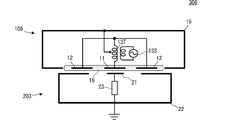
- FIG. 9 is a sectional view conceptually illustrating a relevant portion of a power transfer system 305 according to a Fifth Embodiment.
- FIG. 10 is a sectional view conceptually illustrating a relevant portion of a power transfer system 306 according to a Sixth Embodiment.
- FIG. 11 is a circuit diagram of a power reception device 201 according to a Seventh Embodiment.
- FIG. 2 is a sectional view conceptually illustrating a relevant portion of a power transfer system 301.
- FIG. 3A is a bottom view of a power reception device 201 and
- FIG. 3B is a top view of a power transmission device 101.
- the power transfer system 301 comprises the power transmission device 101 and the power reception device 201.
- a central conductor 11 serving as a power transmission device side active electrode and a peripheral conductor 12 which surrounds the central conductor 11 in a manner isolated therefrom and serves as a power transmission device side passive electrode.
- a high-frequency high-voltage generating circuit 13 is provided which is configured to apply a high voltage of high frequency between the central conductor 11 and the peripheral conductor 12.
- the peripheral conductor 12 is disposed along an inner peripheral surface of the casing 10. Therefore, the high-frequency high-voltage generating circuit 13 is covered with the peripheral conductor 12.
- the casing 10 of the power transmission device 101 is a molding of a plastic, such as ABS resin for example, and is molded integrally therein with the central conductor 11 and the peripheral conductor 12, so that the casing 10 has an outer surface having an insulating structure.
- a central conductor 21 serving as a power reception device side active electrode and a peripheral conductor 22 which surrounds the central conductor 21 in a manner isolated therefrom and serves as a power reception device side passive electrode.
- a load circuit 23 is provided which receives electric power induced between the central conductor 21 and the peripheral conductor 22.
- the peripheral conductor 22 is disposed along an inner peripheral surface of the casing 20. Therefore, the load circuit 23 is covered with the peripheral conductor 22.
- the casing 20 of the power reception device 201 is also a molding of a plastic, such as ABS resin for example, and is molded integrally therein with the central conductor 21 and the peripheral conductor 22, so that the casing 20 has an outer surface having an insulating structure.
- a plastic such as ABS resin for example
- the central conductor 11 of the power transmission device 101 is shaped circular.
- the peripheral conductor 12 has a circular opening portion A1 positioned concentrically with the central conductor 11. That is, the peripheral conductor 12 is disposed in a position to surround the central conductor 11 in a manner isolated from the central conductor 11.
- the central conductor 21 of the power reception device 201 is also shaped circular.
- the peripheral conductor 22 has a circular opening portion A2 positioned concentrically with the central conductor 21 and is disposed in a position to surround the central conductor 21 in a manner isolated from the central conductor 21.
- the central conductors 11 and 21 have substantially the same size.
- the opening portions A1 and A2 of the peripheral conductors have substantially the same size.
- the coupling capacitance between the peripheral conductors 12 and 22 as the passive electrodes can be made relatively larger than the coupling capacitance between the central conductors 11 and 12 as the active electrodes.
- a voltage applied to each peripheral conductor can be lowered according to the ratio between divided voltages obtained by division by capacitances.
- the peripheral conductor 12 formed in proximity to the upper surface of the power transmission device 101 faces the peripheral conductor 22 formed in proximity to the lower surface of the power reception device 201.
- a capacitance takes place between the opposed portions of the central conductors 11 and 12 and a capacitance takes place between the peripheral conductors 12 and 22, particularly between the opposed portions of their acting surfaces. That is, the central conductors 11 and 21 and the peripheral conductors 12 and 22 act as capacitively coupled electrodes.
- the high-frequency high-voltage generating circuit 13 includes a coil transformer, a piezoelectric transformer, an LC resonant circuit, or the like and is a circuit configured to generate a high voltage having a high frequency of, for example, from 100 kHz to several tens of MHz.
- the load circuit 23 includes a high-voltage circuit (including a transformer, a resonant circuit and the like), a rectifying smoothing circuit, and a low-voltage circuit which is operated by an output voltage of the rectifying smoothing circuit.
- the rectifying and smoothing circuit comprises a diode bridge circuit and a smoothing capacitor.
- the alternating load is supplied with an alternating voltage using a step-down transformer, a voltage dividing circuit, or the like which directly lowers an alternating voltage without rectification.
- the reference voltage of the peripheral conductor 12 of the power transmission device 101 is the reference voltage (ground potential) of the high-frequency high-voltage generating circuit 13.
- the reference voltage of the peripheral conductor 22 of the power reception device 201 is the reference voltage (ground potential) of the load circuit 23. Therefore, the central conductors 11 and 21 function as high-voltage side active electrodes, while the peripheral conductors 12 and 22 function as low-voltage side passive electrodes.
- An auxiliary high-frequency high-voltage generating circuit 33 which is equivalent to the "potential control section" defined by the present invention, is connected between the peripheral conductor 12 of the power transmission device 101 and a ground of the power transmission device 101.
- the auxiliary high-frequency high-voltage generating circuit 33 generates a high voltage synchronously with the high-frequency high-voltage generating circuit 13 and controls the potential of the peripheral conductor 12 of the power transmission device 101 by applying a high-frequency voltage to the peripheral conductor 12 of the power transmission device 101. Since the peripheral conductor 12 of the power transmission device 101 and the peripheral conductor 22 of the power reception device 201 are capacitively coupled to each other, the potential of the peripheral conductor 22 of the power reception device 201 changes with a change in the potential of the peripheral conductor 12 of the power transmission device 101.
- the potential of the peripheral conductor 12 of the power transmission device 101 is controlled so as to suppress a change in the potential of the peripheral conductor 22 of the power reception device 201 relative to the ground potential of the power transmission device 101.
- the auxiliary high-frequency high-voltage generating circuit 33 generates a high voltage of an opposite phase to that generated by the high-frequency high-voltage generating circuit 13.
- the auxiliary high-frequency high-voltage generating circuit 33 and the high-frequency high-voltage generating circuit 13 may be formed using a high-frequency high-voltage power source circuit having two output terminals.
- the potential of the peripheral conductor 22 is varied particularly by capacitive coupling between the central conductor 11 of the power transmission device 101 and the peripheral conductor 22 of the power reception device 201.
- the voltage generated by the auxiliary high-frequency high-voltage generating circuit 33 acts in such a direction as to cancel such a variation and, hence, the potential of the peripheral conductor 22 of the power reception device 201 is virtually grounded.
- the basic principle of the power transfer system according to the present invention is short-range energy transfer using an alternative electromagnetic field (quasi-static electric/magnetic field).
- a wavelength (lambda) is sufficiently longer than the size or operating range (distance d) of an electric field oscillating source, that is, when the relationship: d/(lambda) ⁇ 1 is satisfied, a quasi-static electric field stays (is bound) near the electric field oscillating source.
- a radiant quantity to a distant place is negligibly small.
- FIG. 4 is an equivalent circuit diagram of the power transfer system 301.
- capacitive coupling portions are represented as two series capacitances.
- a source side dipole is formed of the central conductor 11 as the power transmission device side active electrode, the peripheral conductor 12 as the power transmission device side passive electrode, and the high-frequency high-voltage generating circuit 13.
- a load side dipole is formed of the central conductor 21 as the power reception device side active electrode, the peripheral conductor 22 as the power reception device side passive electrode, and the load circuit 23.
- the auxiliary high-frequency high-voltage generating circuit 33 controls its voltage V1 so that the voltage V4 of the peripheral conductor 22 forming the passive electrode of the load side dipole assumes zero.
- the auxiliary high-frequency high-voltage generating circuit 33 is simply caused to generate the voltage V1 represented by the following expression synchronously (in-phase) with the voltage generated by the high-frequency high-voltage generating circuit 13. This expression can be derived from conditions for the potential V4 to assume zero.
- FIG. 5 plots results obtained by calculating the magnitude of the potential V4 of the load side passive electrode under a condition controlled or not controlled by the auxiliary high-frequency high-voltage generating circuit 33.
- Cp represents the capacitance between the passive electrodes
- Ca represents the capacitance between the active electrodes
- the abscissa takes on Cp/Ca
- the ordinate takes on the potential V4 of the load side passive electrode.
- characteristic curve A depicts the potential controlled by the auxiliary high-frequency high-voltage generating circuit 33 and characteristic curve B depicts the potential not controlled.
- the potential V4 of the load side passive electrode lowers as the capacitance ratio Cp/Ca increases. Also, the potential V4 can be set to zero regardless of the capacitance ratio Cp/Ca by controlling the auxiliary high-frequency high-voltage generating circuit 33.
- the potential of the passive electrode (peripheral conductor 22) of the power reception device 201 can be controlled from the power transmission device 101 side. Since the control is performed to cause the potential of the passive electrode of the power reception device 201 to assume the ground potential, the leakage of unnecessary electromagnetic field from the passive electrode of the power reception device 201 can be reduced. It is also possible to shield the active electrode (central conductor 11) of the power transmission device 101 and the active electrode (central conductor 21) of the power reception device 201 with the passive electrode (peripheral conductor 12) of the power transmission device 101 and the passive electrode (peripheral conductor 22) of the power transmission device 201.
- each central conductor and the portion of the peripheral conductor paired therewith which extends at the associated acting surface are formed in substantially the same plane, the central conductors 11 and 21 and the peripheral conductors 12 and 22 can be easily formed at the acting surfaces, thus making it possible to render the gap between opposite electrodes constant and stabilize the power transfer characteristics.
- FIG. 6 is a sectional view conceptually illustrating a relevant portion of a power transfer system 302 according to a Second Embodiment.
- the power transfer system 302 comprises a power transmission device 102 and the power reception device 201.
- the power reception device 201 has the same configuration as the power reception device 201 shown in FIG. 2 and includes the central conductor 21, peripheral conductor 22 and load circuit 23 within the casing 20.
- the central conductor 11 serving as a power transmission device side active electrode and the peripheral conductor 12 which surrounds the central conductor 11 in a manner isolated therefrom and serves as a power transmission device side passive electrode.
- the high-frequency high-voltage generating circuit 13 is provided which is configured to apply a high voltage of high frequency between the central conductor 11 and the peripheral conductor 12.
- a detection electrode 331 is provided in proximity to an upper surface of the casing 10 of the power transmission device 102 so as to face the peripheral conductor 22 of the power reception device 201.
- An auxiliary high-frequency high-voltage generator 333 and a voltage control circuit 332 are provided inside the power transmission device 102.
- the detection electrode 331 is capacitively coupled to the peripheral conductor 22 of the power reception device 201.
- the voltage control circuit 332 detects the potential of the peripheral conductor 22 of the power reception device 201 by way of the potential of the detection electrode 331.
- the voltage control circuit 332 also controls the auxiliary high-frequency high-voltage generator 333 according to the potential of the peripheral conductor 22 of the power reception device 201.
- the auxiliary high-frequency high-voltage generating circuit 33 generates a fixed voltage such as to make the potential of the peripheral conductor 22 of the power reception device 210 equivalently equal to the ground potential of the power transmission device 102.
- the voltage generated by the auxiliary high-frequency high-voltage generator 333 is feedback-controlled so that the potential of concern becomes equivalently equal to the ground potential of the power transmission device 102.
- the auxiliary high-frequency high-voltage generator 333 generates a high voltage synchronously with the high-frequency high-voltage generating circuit 13 and applies a high-frequency voltage to the peripheral conductor 12 of the power transmission device 102, thereby controlling the potential of the peripheral conductor 12 of the power transmission device 102. Since the peripheral conductor 12 of the power transmission device 102 and the peripheral conductor 22 of the power reception device 201 are capacitively coupled to each other, the potential of the peripheral conductor 22 of the power reception device 201 changes with a change in the potential of the peripheral conductor 12 of the power transmission device 102. By utilizing this action the potential of the peripheral conductor 12 of the power transmission device 102 is controlled so as to suppress a change in the potential of the peripheral conductor 22 of the power reception device 201 relative to the ground potential of the power transmission device 102.
- the auxiliary high-frequency high-voltage generator 333 generates a voltage that is different in voltage value (amplitude) from that generated by the high-frequency high-voltage generating circuit 13. These voltages may have the same polarity.
- a power source circuit for the auxiliary high-frequency high-voltage generator 333 and a power source circuit for the high-frequency high-voltage generating circuit 13 may be formed using a high-frequency high-voltage power source circuit having two output terminals.
- the capacitance which takes place between opposite electrodes respectively belonging to the power transmission device 102 and the power reception device 201 changes depending on the size of the power reception device and the manner of placement of the power reception device relative to the power transmission device. Therefore, the potential of the peripheral conductor 22 of the power reception device 201 changes depending on the size of the power reception device and the manner of placement of the power reception device relative to the power transmission device. According to the Second Embodiment, however, the feedback control makes it possible to more stably and constantly render the potential of the peripheral conductor 22 of the power reception device 201 substantially equal to the ground potential of the power transmission device equivalently.
- FIG. 7 is a sectional view conceptually illustrating a relevant portion of a power transfer system 303 according to a Third Embodiment.
- the power transfer system 303 comprises a power transmission device 103 and the power reception device 201.
- the power reception device 201 has the same configuration as the power reception device 201 shown in FIG. 2 and includes the central conductor 21, peripheral conductor 22 and load circuit 23 within the casing 20.
- the guard electrode 15 is shaped to surround the peripheral conductor 12 serving as a power transmission device 103 side passive electrode and has a potential set to the ground potential.
- the guard electrode 15 is located near the peripheral conductor 22 serving as a power reception device 201 side passive electrode and is capacitively coupled thereto partially. Since the guard electrode 15 is capacitively coupled to the peripheral conductor 22, the potential of the peripheral conductor 22 can be brought closer to the ground potential.
- the detection electrode 331 is surrounded with the guard electrode 15.
- the guard electrode 15 need not necessarily surround the entire circumference of the peripheral conductor 12 as the power transmission device 103 side passive electrode and may be partially formed with a slit-like gap for example.
- the voltage control circuit 332 detects the potential of the peripheral conductor 22 of the power reception device 201 by way of the potential of the detection electrode 331 and controls the auxiliary high-frequency high-voltage generator 333 so that the potential of the peripheral conductor 22 becomes equivalently equal to the ground potential.
- FIG. 8 is a sectional view conceptually illustrating a relevant portion of a power transfer system 304 according to a Fourth Embodiment.
- the power transfer system 304 comprises a power transmission device 104 and the power reception device 201.
- the power reception device 201 has the same configuration as the power reception device 201 shown in FIG. 2 and includes the central conductor 21, peripheral conductor 22 and load circuit 23 within the casing 20.
- the guard electrode 15 of the power transmission device 104 surrounds the peripheral conductor 12 as a power transmission device side passive electrode, the voltage control circuit 332 and the auxiliary high-frequency high-voltage generator 333.
- the guard electrode 15 serves as a ground of the casing.
- the ground of the casing may be connected to a ground electrode of a commercial power source.
- This structure not only prevents the detection electrode 331 from being interfered with by the peripheral conductor 12 of the power transmission device 104 but also suppresses the leakage of unnecessary electromagnetic field from the power transmission device 104.
- FIG. 9 is a sectional view conceptually illustrating a relevant portion of a power transfer system 305 according to a Fifth Embodiment.
- the power transfer system 305 comprises a power transmission device 105 and a power reception device 202.
- the power transmission device 105 has an upper surface provided with the central conductor 11 serving as a power transmission device side active electrode and the peripheral conductor 12 which surrounds the central conductor 11 in a manner isolated therefrom and serves as a power transmission device side passive electrode.
- the guard electrode 15, which is equivalent to the "shield electrode” defined by the present invention, is disposed in proximity to the upper surface of the power transmission device 105.
- the guard electrode 15 is grounded virtually.
- the secondary coil of a step-up transformer 13T interconnects the central conductor 11 and the peripheral conductor 12.
- the primary coil of the step-up transformer 13T is connected to a high-frequency high-voltage generating circuit 13S.
- the central conductor 11 and the peripheral conductor 12 are coated with an insulating material 16.
- the central conductor 21 serving as a power reception device side active electrode and the peripheral conductor 22 which surrounds the central conductor 21 in a manner isolated therefrom and serves as a power reception device side passive electrode.
- the load circuit 23 is provided which receives electric power induced between the central conductor 21 and the peripheral conductor 22 of the power reception device 202.
- a circuit portion comprising the secondary coil of the step-up transformer 13T and a tap interconnecting the secondary coil and the guard electrode 15 is equivalent to the "potential control section" defined by the present invention.
- the Fifth Embodiment is capable of generating an application voltage relative to the ground potential of the power transmission device 105 which is to be applied to the power transmission device side passive electrode (peripheral conductor 12) by fixing a ground point of the secondary coil of the step-up transformer 13T. That is, the high-frequency high-voltage generating circuit and the auxiliary high-frequency high-voltage generator can be formed using a single power source.
- the guard electrode 15 which is grounded virtually, assumes substantially the earth potential. For this reason, the guard electrode 15 does not need to be protected by insulation.
- FIG. 10 is a sectional view conceptually illustrating a relevant portion of a power transfer system 306 according to a Sixth Embodiment.
- the power transfer system 306 comprises a power transmission device 106 and a power reception device 203.
- the power transmission device 106 has a lower surface provided with the central conductor 11 serving as a power transmission device side active electrode and the peripheral conductor 12 which surrounds the central conductor 11 in a manner isolated therefrom and serves as a power transmission device side passive electrode.
- the guard electrode 15, which shields the peripheral conductor 12, is disposed to surround the power transmission device 106.
- the guard electrode 15 is connected to a virtual ground of the power transmission device 106.
- the secondary coil of the step-up transformer 13T interconnects the central conductor 11 and the peripheral conductor 12.
- the high-frequency high-voltage generating circuit 13S is connected to the primary coil of the step-up transformer 13T.
- the central conductor 11 and the peripheral conductor 12 are coated with the insulating material 16.
- the central conductor 21 serving as a power reception device side active electrode and the peripheral conductor 22 which surrounds the central conductor 21 in a manner isolated therefrom and serves as a power reception device side passive electrode.
- the load circuit 23 is provided which receives electric power induced between the central conductor 21 and the peripheral conductor 22 of the power reception device 203.
- a circuit portion comprising the secondary coil of the step-up transformer 13T and a tap interconnecting the secondary coil and the guard electrode 15 is equivalent to the "potential control section" defined by the present invention.
- the power transmission device 106 is for use as a battery-driven portable power source.
- the guard electrode 15 which is grounded virtually, assumes substantially the earth potential, as in the Fifth Embodiment. For this reason, the guard electrode 15 does not need to be protected by insulation.
- FIG. 11 is a circuit diagram of the power reception device 201 according to the Seventh Embodiment.
- the load circuit 23 includes a rectifying smoothing circuit 30 and a low-voltage circuit portion 29.
- the rectifying smoothing circuit 30 includes a step-down transformer T, rectifying diodes D1 and D2, and a smoothing capacitor C.
- the primary coil of the transformer T has one end connected to the central conductor 21 and an opposite end connected to the peripheral conductor 22 as a ground of a metal frame.
- the secondary coil of the transformer T is formed with a full-wave rectifying circuit comprising the rectifying diodes D1 and D2 and the smoothing capacitor C.
- the rectifying smoothing circuit 30 may include a resonance circuit. Alternatively, such a resonance circuit may be provided before or after the rectifying smoothing circuit 30.
- the power reception device 201 forms a noncontact charging device and the low-voltage circuit portion 29 includes a control circuit 31 operated by a voltage rectified and smoothed by the rectifying smoothing circuit 30 that serves as a power source, and a secondary battery 32.
- the control circuit 31 performs a charging control for the secondary battery 32, a charging control using the secondary battery 32 as a power source, and other predetermined circuit operations.
- the voltage value (amplitude) of a voltage generated by the auxiliary high-frequency high-voltage generator 333 relative to a voltage generated by the high-frequency high-voltage generating circuit 13 is a subject to be controlled.
- the phase of a voltage generated by the auxiliary high-frequency high-voltage generator 333 may also be a subject to be controlled.
- a feedback control may be performed so that the potential of the peripheral conductor 22 of the power reception device 201 becomes equivalently equal to the ground potential of the power transmission device 201 by controlling the voltage value and the phase of a voltage generated by the auxiliary high-frequency high-voltage generator 333.
- the phase of a waveform representing a potential change of the peripheral conductor 22 of the power reception device 201 is detected and a control is performed so as to minimize the amplitude of the potential change of the peripheral conductor 22 of the power reception device 201.
- This configuration is capable of suppressing the potential change of the peripheral conductor 22 of the power reception device 201 even when there is a phase difference between the potential change of the peripheral conductor 22 of the power reception device 201 and a voltage change of the high-frequency high-voltage generating circuit 13.
- the peripheral conductor 12 serving as the power transmission device side passive electrode surrounds the central conductor 11 serving as the power transmission device side active electrode
- the peripheral conductor 12 need not necessarily surround the central conductor 11.
- the peripheral conductor 22 serving as the power reception device side passive electrode need not necessarily surround the central conductor 21 serving as the power reception device side passive electrode.
- an active electrode and a passive electrode need not necessarily be formed in the same plane.
- the active electrode is formed in front of the passive electrode or the passive electrode is formed in front of the active electrode. That is, it is sufficient that the passive electrode is present in the periphery of the active electrode while the power transmission device side active electrode is opposed to the power reception device side active electrode and the power transmission device side passive electrode opposed to the power reception device side passive electrode.
- A1,A2...opening portion of peripheral conductor 10 ...casing of power reception device 11...central conductor (power transmission device side active electrode) 12...peripheral conductor (power transmission device side passive electrode) 13...high-frequency high-voltage generating circuit 15...guard electrode 16...insulating material 20...casing of power transmission device 21...central conductor (power reception device side active electrode) 22...peripheral conductor (power reception device side passive electrode) 23...load circuit 29...low-voltage circuit portion 30...rectifying smoothing circuit 31...control circuit 32...secondary battery 33...auxiliary high-frequency high-voltage generating circuit 101 to 106...power transmission device 201 to 203...power reception device 301 to 306...power transfer system 331...detection electrode 332...voltage control circuit 333...auxiliary high-frequency high-voltage generator
Landscapes
- Engineering & Computer Science (AREA)
- Power Engineering (AREA)
- Computer Networks & Wireless Communication (AREA)
- Physics & Mathematics (AREA)
- Electromagnetism (AREA)
- Near-Field Transmission Systems (AREA)
- Charge And Discharge Circuits For Batteries Or The Like (AREA)
Abstract
Priority Applications (5)
| Application Number | Priority Date | Filing Date | Title |
|---|---|---|---|
| CN201180009626.3A CN102893494B (zh) | 2011-05-13 | 2011-05-13 | 电力发送设备和电力传输系统 |
| JP2012529837A JP5299578B2 (ja) | 2011-05-13 | 2011-05-13 | 電力送電装置及び電力伝送システム |
| PCT/JP2011/002663 WO2012157011A1 (fr) | 2011-05-13 | 2011-05-13 | Dispositif de transmission d'énergie et système de transfert d'énergie |
| EP11857418.5A EP2707940B1 (fr) | 2011-05-13 | 2011-05-13 | Dispositif de transmission d'énergie et système de transfert d'énergie |
| US13/568,505 US9172276B2 (en) | 2011-05-13 | 2012-08-07 | Power transmission device and power transfer system |
Applications Claiming Priority (1)
| Application Number | Priority Date | Filing Date | Title |
|---|---|---|---|
| PCT/JP2011/002663 WO2012157011A1 (fr) | 2011-05-13 | 2011-05-13 | Dispositif de transmission d'énergie et système de transfert d'énergie |
Related Child Applications (1)
| Application Number | Title | Priority Date | Filing Date |
|---|---|---|---|
| US13/568,505 Continuation US9172276B2 (en) | 2011-05-13 | 2012-08-07 | Power transmission device and power transfer system |
Publications (1)
| Publication Number | Publication Date |
|---|---|
| WO2012157011A1 true WO2012157011A1 (fr) | 2012-11-22 |
Family
ID=47176384
Family Applications (1)
| Application Number | Title | Priority Date | Filing Date |
|---|---|---|---|
| PCT/JP2011/002663 Ceased WO2012157011A1 (fr) | 2011-05-13 | 2011-05-13 | Dispositif de transmission d'énergie et système de transfert d'énergie |
Country Status (5)
| Country | Link |
|---|---|
| US (1) | US9172276B2 (fr) |
| EP (1) | EP2707940B1 (fr) |
| JP (1) | JP5299578B2 (fr) |
| CN (1) | CN102893494B (fr) |
| WO (1) | WO2012157011A1 (fr) |
Cited By (4)
| Publication number | Priority date | Publication date | Assignee | Title |
|---|---|---|---|---|
| WO2014112639A1 (fr) * | 2013-01-21 | 2014-07-24 | 株式会社村田製作所 | Système d'émission de puissance |
| WO2014132518A1 (fr) * | 2013-03-01 | 2014-09-04 | 株式会社村田製作所 | Appareil de transmission de puissance et appareil de réception de puissance |
| WO2014148369A1 (fr) * | 2013-03-19 | 2014-09-25 | 株式会社村田製作所 | Système de transmission d'énergie sans fil |
| EP3413432A1 (fr) * | 2017-06-07 | 2018-12-12 | Panasonic Intellectual Property Management Co., Ltd. | Unité d'électrode, dispositif de transmission de puissance, dispositif de réception de puissance, dispositif électronique, véhicule et système de transmission d'énergie sans fil |
Families Citing this family (10)
| Publication number | Priority date | Publication date | Assignee | Title |
|---|---|---|---|---|
| WO2013145403A1 (fr) * | 2012-03-26 | 2013-10-03 | 株式会社村田製作所 | Système de transmission d'énergie sans fil à liaison par champs électrique, et dispositif d'accès à l'électricité mettant en œuvre celui-ci |
| US9673658B2 (en) * | 2014-03-06 | 2017-06-06 | Samsung Electro-Mechanics Co., Ltd. | Non-contact capacitive coupling type power charging apparatus and non-contact capacitive coupling type battery apparatus |
| CA2953621A1 (fr) | 2014-06-26 | 2015-12-30 | Solace Power Inc. | Systeme de transmission de puissance de champ electrique sans fil, emetteur et recepteur pour ce dernier et procede de transfert sans fil de puissance |
| WO2016033697A1 (fr) | 2014-09-05 | 2016-03-10 | Solace Power Inc. | Système de transfert de puissance de champ électrique sans fil, procédé, émetteur et récepteur associés |
| KR102624324B1 (ko) * | 2016-12-29 | 2024-01-12 | 주식회사 위츠 | 무선 전력 송신 장치 |
| EP3386072A1 (fr) | 2017-04-07 | 2018-10-10 | ABB Schweiz AG | Système de transfert d'énergie sans fil entre potentiel électrique faible et élevé et disjoncteur haute tension |
| CN110829621A (zh) * | 2018-08-09 | 2020-02-21 | 法雷奥舒适驾驶助手公司 | 无线充电装置和用于控制无线充电装置的方法 |
| CN116547887A (zh) * | 2020-11-19 | 2023-08-04 | 阿萨夫·马诺娃·埃尔西博尼 | 无线电力传输系统和方法 |
| JP7740526B2 (ja) * | 2022-04-08 | 2025-09-17 | Ntt株式会社 | 電力伝送装置 |
| IL317082A (en) * | 2022-05-17 | 2025-01-01 | ELSSWAY Ltd | Wireless power transfer system and method |
Citations (3)
| Publication number | Priority date | Publication date | Assignee | Title |
|---|---|---|---|---|
| JP2009296857A (ja) * | 2008-06-09 | 2009-12-17 | Sony Corp | 伝送システム、給電装置、受電装置、及び伝送方法 |
| JP2010213554A (ja) * | 2009-03-12 | 2010-09-24 | Takenaka Komuten Co Ltd | 電力供給システム |
| JP2010537613A (ja) * | 2007-08-17 | 2010-12-02 | Tmms株式会社 | 電気双極子間の近接場における遠隔縦結合によって電気エネルギを伝達し、分配し、かつ管理するための方法および装置 |
Family Cites Families (8)
| Publication number | Priority date | Publication date | Assignee | Title |
|---|---|---|---|---|
| JPH09312942A (ja) | 1996-05-21 | 1997-12-02 | Hitachi Ltd | 非接触式集電方法およびその装置 |
| CN2694287Y (zh) * | 2004-03-09 | 2005-04-20 | 中国科学院空间科学与应用研究中心 | 一种电场测量仪器的标定装置 |
| FR2875649B1 (fr) | 2004-09-21 | 2010-09-24 | Henri Bondar | Dispositif de transport a distance par influence de l'energie electrique sans fil ni terre comme conducteur de l iaison |
| CN101416411B (zh) | 2006-03-21 | 2013-05-15 | 株式会社村田制作所 | 通过穿越电介质的局部感应传输能量的装置 |
| JP4399481B2 (ja) | 2007-06-29 | 2010-01-13 | シャープ株式会社 | 帯電装置、画像形成装置、帯電装置の制御方法、制御プログラム、及び当該制御プログラムを記録したコンピュータ読み取り可能な記録媒体 |
| JP5433225B2 (ja) | 2008-12-24 | 2014-03-05 | 学校法人東京理科大学 | インクジェット用インク |
| JP5354030B2 (ja) | 2009-06-25 | 2013-11-27 | 株式会社村田製作所 | 電力伝送システム及び非接触充電装置 |
| CN102804549B (zh) * | 2009-06-25 | 2013-08-21 | 株式会社村田制作所 | 功率传送系统和非接触充电装置 |
-
2011
- 2011-05-13 CN CN201180009626.3A patent/CN102893494B/zh active Active
- 2011-05-13 JP JP2012529837A patent/JP5299578B2/ja active Active
- 2011-05-13 WO PCT/JP2011/002663 patent/WO2012157011A1/fr not_active Ceased
- 2011-05-13 EP EP11857418.5A patent/EP2707940B1/fr active Active
-
2012
- 2012-08-07 US US13/568,505 patent/US9172276B2/en active Active
Patent Citations (3)
| Publication number | Priority date | Publication date | Assignee | Title |
|---|---|---|---|---|
| JP2010537613A (ja) * | 2007-08-17 | 2010-12-02 | Tmms株式会社 | 電気双極子間の近接場における遠隔縦結合によって電気エネルギを伝達し、分配し、かつ管理するための方法および装置 |
| JP2009296857A (ja) * | 2008-06-09 | 2009-12-17 | Sony Corp | 伝送システム、給電装置、受電装置、及び伝送方法 |
| JP2010213554A (ja) * | 2009-03-12 | 2010-09-24 | Takenaka Komuten Co Ltd | 電力供給システム |
Non-Patent Citations (1)
| Title |
|---|
| See also references of EP2707940A4 * |
Cited By (13)
| Publication number | Priority date | Publication date | Assignee | Title |
|---|---|---|---|---|
| WO2014112639A1 (fr) * | 2013-01-21 | 2014-07-24 | 株式会社村田製作所 | Système d'émission de puissance |
| US10014720B2 (en) | 2013-01-21 | 2018-07-03 | Murata Manufacturing Co., Ltd. | Power transmission system |
| JP5979301B2 (ja) * | 2013-03-01 | 2016-08-24 | 株式会社村田製作所 | 送電装置および受電装置 |
| WO2014132518A1 (fr) * | 2013-03-01 | 2014-09-04 | 株式会社村田製作所 | Appareil de transmission de puissance et appareil de réception de puissance |
| JP5790897B2 (ja) * | 2013-03-19 | 2015-10-07 | 株式会社村田製作所 | ワイヤレス電力伝送システム |
| GB2526711A (en) * | 2013-03-19 | 2015-12-02 | Murata Manufacturing Co | Wireless power transmission system |
| CN105191061A (zh) * | 2013-03-19 | 2015-12-23 | 株式会社村田制作所 | 无线电力传输系统 |
| WO2014148369A1 (fr) * | 2013-03-19 | 2014-09-25 | 株式会社村田製作所 | Système de transmission d'énergie sans fil |
| CN105191061B (zh) * | 2013-03-19 | 2017-11-14 | 株式会社村田制作所 | 无线电力传输系统 |
| US9866038B2 (en) | 2013-03-19 | 2018-01-09 | Murata Manufacturing Co., Ltd. | Wireless power transmission system |
| GB2526711B (en) * | 2013-03-19 | 2019-05-29 | Murata Manufacturing Co | Wireless power transmission system |
| EP3413432A1 (fr) * | 2017-06-07 | 2018-12-12 | Panasonic Intellectual Property Management Co., Ltd. | Unité d'électrode, dispositif de transmission de puissance, dispositif de réception de puissance, dispositif électronique, véhicule et système de transmission d'énergie sans fil |
| US11005296B2 (en) | 2017-06-07 | 2021-05-11 | Panasonic Intellectual Property Management Co., Ltd. | Electrode unit, power transmitting device, power receiving device, electronic device, vehicle, and wireless power transmission system |
Also Published As
| Publication number | Publication date |
|---|---|
| EP2707940A4 (fr) | 2015-07-08 |
| CN102893494B (zh) | 2015-10-21 |
| CN102893494A (zh) | 2013-01-23 |
| US20120299397A1 (en) | 2012-11-29 |
| JP2013534124A (ja) | 2013-08-29 |
| EP2707940A1 (fr) | 2014-03-19 |
| EP2707940B1 (fr) | 2016-08-10 |
| JP5299578B2 (ja) | 2013-09-25 |
| US9172276B2 (en) | 2015-10-27 |
Similar Documents
| Publication | Publication Date | Title |
|---|---|---|
| US9172276B2 (en) | Power transmission device and power transfer system | |
| EP2727216B1 (fr) | Dispositif de puissance haute fréquence, dispositif de transmission de puissance et système de transfert de puissance | |
| CN102754306B (zh) | 功率传输系统 | |
| US8907617B2 (en) | Power transfer system and noncontact charging device | |
| US10153664B2 (en) | Wireless power transmission system and power transmitter | |
| US9698629B2 (en) | Wireless power transmission system, power transmitting device, and power receiving device | |
| US10014720B2 (en) | Power transmission system | |
| US8536739B2 (en) | Power transfer system and noncontact charging device | |
| KR101604172B1 (ko) | 전계 결합형 무선 충전장치 | |
| US10320279B2 (en) | Power supplies and methods for reducing common mode noise | |
| KR102730330B1 (ko) | 보조 코일을 이용한 무선 전력 송신 장치, 무선 전력 수신 장치 및 무선 전력 전송 시스템 |
Legal Events
| Date | Code | Title | Description |
|---|---|---|---|
| WWE | Wipo information: entry into national phase |
Ref document number: 201180009626.3 Country of ref document: CN |
|
| ENP | Entry into the national phase |
Ref document number: 2012529837 Country of ref document: JP Kind code of ref document: A |
|
| REEP | Request for entry into the european phase |
Ref document number: 2011857418 Country of ref document: EP |
|
| WWE | Wipo information: entry into national phase |
Ref document number: 2011857418 Country of ref document: EP |
|
| 121 | Ep: the epo has been informed by wipo that ep was designated in this application |
Ref document number: 11857418 Country of ref document: EP Kind code of ref document: A1 |
|
| NENP | Non-entry into the national phase |
Ref country code: DE |