WO2012157161A1 - Procédé de lavage de composants d'un appareil de fabrication de semi-conducteurs, appareil de lavage d'un composant d'un appareil de fabrication de semi-conducteurs, et appareil de croissance en phase vapeur - Google Patents
Procédé de lavage de composants d'un appareil de fabrication de semi-conducteurs, appareil de lavage d'un composant d'un appareil de fabrication de semi-conducteurs, et appareil de croissance en phase vapeur Download PDFInfo
- Publication number
- WO2012157161A1 WO2012157161A1 PCT/JP2012/001829 JP2012001829W WO2012157161A1 WO 2012157161 A1 WO2012157161 A1 WO 2012157161A1 JP 2012001829 W JP2012001829 W JP 2012001829W WO 2012157161 A1 WO2012157161 A1 WO 2012157161A1
- Authority
- WO
- WIPO (PCT)
- Prior art keywords
- semiconductor manufacturing
- cleaning
- manufacturing apparatus
- gas
- component
- Prior art date
- Legal status (The legal status is an assumption and is not a legal conclusion. Google has not performed a legal analysis and makes no representation as to the accuracy of the status listed.)
- Ceased
Links
Images




Classifications
-
- H—ELECTRICITY
- H10—SEMICONDUCTOR DEVICES; ELECTRIC SOLID-STATE DEVICES NOT OTHERWISE PROVIDED FOR
- H10P—GENERIC PROCESSES OR APPARATUS FOR THE MANUFACTURE OR TREATMENT OF DEVICES COVERED BY CLASS H10
- H10P70/00—Cleaning of wafers, substrates or parts of devices
-
- H—ELECTRICITY
- H10—SEMICONDUCTOR DEVICES; ELECTRIC SOLID-STATE DEVICES NOT OTHERWISE PROVIDED FOR
- H10P—GENERIC PROCESSES OR APPARATUS FOR THE MANUFACTURE OR TREATMENT OF DEVICES COVERED BY CLASS H10
- H10P50/00—Etching of wafers, substrates or parts of devices
-
- C—CHEMISTRY; METALLURGY
- C23—COATING METALLIC MATERIAL; COATING MATERIAL WITH METALLIC MATERIAL; CHEMICAL SURFACE TREATMENT; DIFFUSION TREATMENT OF METALLIC MATERIAL; COATING BY VACUUM EVAPORATION, BY SPUTTERING, BY ION IMPLANTATION OR BY CHEMICAL VAPOUR DEPOSITION, IN GENERAL; INHIBITING CORROSION OF METALLIC MATERIAL OR INCRUSTATION IN GENERAL
- C23C—COATING METALLIC MATERIAL; COATING MATERIAL WITH METALLIC MATERIAL; SURFACE TREATMENT OF METALLIC MATERIAL BY DIFFUSION INTO THE SURFACE, BY CHEMICAL CONVERSION OR SUBSTITUTION; COATING BY VACUUM EVAPORATION, BY SPUTTERING, BY ION IMPLANTATION OR BY CHEMICAL VAPOUR DEPOSITION, IN GENERAL
- C23C16/00—Chemical coating by decomposition of gaseous compounds, without leaving reaction products of surface material in the coating, i.e. chemical vapour deposition [CVD] processes
- C23C16/44—Chemical coating by decomposition of gaseous compounds, without leaving reaction products of surface material in the coating, i.e. chemical vapour deposition [CVD] processes characterised by the method of coating
- C23C16/4401—Means for minimising impurities, e.g. dust, moisture or residual gas, in the reaction chamber
- C23C16/4405—Cleaning of reactor or parts inside the reactor by using reactive gases
-
- H—ELECTRICITY
- H10—SEMICONDUCTOR DEVICES; ELECTRIC SOLID-STATE DEVICES NOT OTHERWISE PROVIDED FOR
- H10P—GENERIC PROCESSES OR APPARATUS FOR THE MANUFACTURE OR TREATMENT OF DEVICES COVERED BY CLASS H10
- H10P72/00—Handling or holding of wafers, substrates or devices during manufacture or treatment thereof
- H10P72/04—Apparatus for manufacture or treatment
- H10P72/0402—Apparatus for fluid treatment
- H10P72/0406—Apparatus for fluid treatment for cleaning followed by drying, rinsing, stripping, blasting or the like
Definitions
- the present invention relates to a method for cleaning a semiconductor manufacturing apparatus component, a cleaning apparatus for a semiconductor manufacturing apparatus component, and a vapor phase growth apparatus.
- a nitride semiconductor manufacturing apparatus manufactures a semiconductor by depositing a nitride such as GaN (gallium nitride) or AlGaN (gallium aluminum nitride) on a silicon wafer.
- a semiconductor thin film such as GaN to be deposited on the wafer in the semiconductor manufacturing apparatus adheres to various parts other than the wafer, such as a wafer tray and a gas flow path for holding the wafer. Since GaN or the like adhering to parts other than the wafer becomes an unnecessary contaminant and obstructs the manufacture of the nitride semiconductor, it is necessary to clean the contaminated part and remove the nitride.
- nitrides such as GaN and AlGaN are reacted with a cleaning gas mainly composed of a chlorine-based gas to remove nitrides adhering to semiconductor manufacturing equipment components.
- Patent Document 1 Japanese Patent Application Laid-Open No. 2006-332201
- a contaminated component in a nitride semiconductor manufacturing apparatus is brought into contact with a cleaning gas mainly containing a chlorine-based gas at a temperature of 500 ° C. or higher and 1000 ° C. or lower.
- a cleaning method is described.
- contaminated component nitrides react with chlorinated gases in the cleaning gas. It is said that the reaction product to be generated is vaporized and removed at a temperature of 500 ° C. or higher. Further, since this method does not require a high temperature of 1000 ° C. or higher, it is said that the wafer tray is not thermally deformed.
- Patent Document 2 Japanese Patent Application Laid-Open No. 2010-245376 describes a cleaning apparatus in which a cleaning gas introduction pipe is disposed in the lower part of the reaction chamber. Since the cleaning gas introduction pipe is arranged in the lower part of the reaction chamber, the cleaning gas introduced into the reaction chamber does not collide with the heat shield member and flow out. Therefore, it is said that the cleaning gas can be efficiently used for cleaning contaminated parts.
- Patent Document 3 Japanese Patent Laid-Open No. 2010-212400
- a sealing surface is provided on the sealing surface side of a sealing cap that closes both end openings of a reaction tube having a cleaning gas introduction tube and an exhaust gas discharge tube.
- a nitride semiconductor device component cleaning device is provided that includes an adhesion-preventing plate provided in close proximity so as to have a space therebetween. Adhesion of the reaction product to the inner wall of the sealing cap can be suppressed by the adhesion preventing plate. Therefore, when removing the cleaned parts by opening the reaction tube after cleaning, the reaction product and moisture in the air do not react to generate toxic gas, and the worker can safely perform the cleaning work. It is supposed to be possible.
- reaction products of nitrides such as GaN and AlGaN and chlorine-based gas may adhere to semiconductor manufacturing equipment components and cleaning equipment, and during the cleaning operation. It was necessary to continuously remove the reaction product. At this time, a part of the unused cleaning gas is also removed together with the reaction product, so that it is necessary to continuously supply the cleaning gas into the apparatus. For this reason, a large amount of cleaning gas is required to remove the contaminants.
- Patent Document 4 Japanese Patent Application Laid-Open No. 2007-109928
- a contaminated component in a nitride semiconductor manufacturing apparatus is brought into contact with a first cleaning gas mainly composed of a chlorine-based gas to thereby remove contaminants.
- a method of cleaning a nitride semiconductor manufacturing apparatus component is described, wherein the chlorine-based material remaining in the component is removed by removing and contacting with a second cleaning gas.
- Patent Document 4 describes that the contact with the first cleaning gas and the contact with the second cleaning gas are performed by a batch processing (sealing) method. In this document, it is shown that the amount of chlorine gas used can be reduced by the sealing method compared with the ventilation treatment (air flow) method.
- Patent Document 4 the present inventors tried to clean the semiconductor manufacturing apparatus parts by the sealing method, and as a result, the amount of chlorine gas used could be reduced to some extent than the air flow method. . However, the cleaning efficiency was still low, and it was confirmed that there was room for further improvement.
- the present invention has been made in view of the above circumstances, and provides a semiconductor manufacturing apparatus component cleaning method and a semiconductor manufacturing apparatus component cleaning apparatus capable of reducing the amount of cleaning gas used and having excellent cleaning efficiency. .
- the present invention has been made in view of the above circumstances, and provides a vapor phase growth apparatus excellent in yield.
- a nitride semiconductor represented by the general formula Al x In y Ga 1-xy N (where x and y are 0 ⁇ x ⁇ 1, 0 ⁇ y ⁇ 1, 0 ⁇ x + y ⁇ 1) is attached.
- the pressure in the apparatus in the third step is 10 kPa or more and 90 kPa or less.
- the reaction rate between the nitride semiconductor and the halogen-containing gas is increased, and it adheres to the semiconductor manufacturing apparatus components.
- the nitride semiconductor can be removed efficiently.
- the mean free path of the reaction product of the nitride semiconductor and the halogen-containing gas can be lengthened by setting the pressure in the apparatus to 90 kPa or less, the diffusion efficiency of the reaction product increases, and the nitride and halogen-containing gas Reaction efficiency can be increased. Therefore, it is possible to reduce the amount of cleaning gas used to remove the deposited nitride semiconductor.
- a nitride semiconductor represented by the general formula Al x In y Ga 1-xy N (where x and y are 0 ⁇ x ⁇ 1, 0 ⁇ y ⁇ 1, 0 ⁇ x + y ⁇ 1) is attached.
- An apparatus for cleaning semiconductor manufacturing equipment parts A component holding unit for holding the semiconductor manufacturing apparatus component; A gas introduction pipe for introducing a halogen-containing gas that reacts with the nitride semiconductor; Capturing means for capturing a reaction product of the nitride semiconductor and the halogen-containing gas;
- a cleaning apparatus for semiconductor manufacturing apparatus parts comprising a gas discharge pipe for discharging the reaction product.
- the reaction product is captured by the capture means by providing the cleaning device with the capture means for capturing the reaction product, the reaction product is undesired in the semiconductor manufacturing apparatus component or the cleaning apparatus. It can suppress adhering to. Therefore, it is not necessary to continuously introduce the cleaning gas and remove the reaction product, and the amount of the cleaning gas used for removing the deposited nitride semiconductor can be reduced.
- a first source gas containing gallium and a second source gas containing ammonia are supplied to the substrate in the reaction vessel, and the general formula Al x In y Ga 1-xy N ( Where x and y are 0 ⁇ x ⁇ 1, 0 ⁇ y ⁇ 1, and 0 ⁇ x + y ⁇ 1)).
- a substrate holding unit for holding the substrate;
- a gas introduction pipe for introducing a halogen-containing gas;
- a vapor phase growth apparatus including a gas discharge pipe for discharging the reaction product is provided.
- a semiconductor manufacturing apparatus component cleaning method and a semiconductor manufacturing apparatus component cleaning apparatus that can reduce the amount of cleaning gas used and that are excellent in cleaning efficiency.
- a vapor phase growth apparatus excellent in yield is provided.
- FIG. 1 is a cross-sectional view showing a configuration of a cleaning apparatus in the first embodiment.
- the cleaning apparatus 100 is represented by the general formula Al x In y Ga 1-xy N (where x and y are 0 ⁇ x ⁇ 1, 0 ⁇ y ⁇ 1, and 0 ⁇ x + y ⁇ 1).
- a component holding unit 102 for holding the semiconductor manufacturing apparatus component 101 to which the nitride semiconductor is adhered
- a reaction tank 103 for storing the component holding unit 102
- a gas introduction pipe 104 for introducing a halogen-containing gas that reacts with the nitride semiconductor
- a gas discharge pipe 105 for discharging reaction products generated in the reaction tank 103 is formed.
- a heating device 106 that heats the inside of the reaction tank 103 and a pressure gauge 108 that monitors the pressure inside the reaction tank 103 can be provided around the reaction tank 103.
- the material of the reaction vessel 103 is not particularly limited, but is formed of a heat resistant material such as quartz. Inside the reaction vessel 103, a component holding unit 102 for holding the semiconductor manufacturing apparatus component 101 is provided. Further, the shape and size of the reaction vessel 103 are not particularly limited, but can be determined as appropriate depending on the size and processing amount of the semiconductor manufacturing apparatus component 101 to be cleaned.
- the component holding unit 102 is a member for holding the semiconductor manufacturing apparatus component 101, and is formed of a heat resistant material such as carbon or quartz.
- the component holding unit 102 is configured to support the semiconductor manufacturing apparatus component 101 and to hold the state. At this time, the entire surface of the semiconductor manufacturing apparatus component 101 is preferably held so as to be processed.
- the configuration for holding the semiconductor manufacturing apparatus component 101 is not particularly limited.
- a configuration in which a groove into which a part of the semiconductor manufacturing apparatus component 101 can be inserted is provided on the surface of the component holding unit 102.
- the semiconductor manufacturing apparatus component 101 can be held by being inserted into the groove.
- the component holding unit 102 may have a configuration in which a hooking unit for hooking and holding the semiconductor manufacturing apparatus component 101 is formed. Since the hook-type component holding unit 102 hooks and holds the semiconductor manufacturing apparatus component 101, the contact area between the semiconductor manufacturing apparatus component 101 and the component holding unit 102 can be minimized. The unwashed portion of the substrate can be minimized.
- a plurality of through holes may be formed in the component holding unit 102.
- the halogen-containing gas supplied from below tends to flow upward.
- the halogen-containing gas can easily come into contact with the semiconductor manufacturing apparatus component 101 held by the component holding unit 102, and the cleaning process of the component holding unit 102 can be performed more efficiently.
- the shape of the through hole is not particularly limited as long as the component holding unit 102 can maintain the strength capable of holding the semiconductor manufacturing apparatus component 101.
- the shape of the through hole may be square or round.
- the component holding unit 102 may be formed in a lattice shape.
- the halogen-containing gas is introduced into the reaction vessel 103 from the container 109 filled with the halogen-containing gas through the gas introduction pipe 104. Further, if necessary, the concentration of the halogen-containing gas can be adjusted by introducing the inert gas into the reaction vessel 103 from the container 110 filled with the inert gas as well as introducing the halogen-containing gas. At this time, the introduction amount of the halogen-containing gas and the inert gas can be adjusted by the gas introduction valve 111.
- the gas discharge pipe 105 is connected to the vacuum pump 113 via the gas discharge valve 112, whereby the inside of the reaction tank 103 can be put into a reduced pressure state. Furthermore, the gas exhaust pipe 105 and the vacuum pump 113 can be connected to an exhaust gas abatement treatment apparatus (not shown) as necessary, detoxify the reaction product discharged from the reaction tank 103, and discharge it to the atmosphere. Can do.
- connection part is not particularly limited.
- the heating device 106 is not particularly limited, but includes, for example, a heating unit that can heat the inside of the reaction vessel 103 and a temperature regulator that can maintain the inside of the reaction vessel 103 at a constant temperature by adjusting the output of the heating unit. Composed.
- the heating means is not particularly limited, and any known heating means such as a heating wire or lamp heating can be used, and any heating means that can heat the semiconductor manufacturing apparatus component 101 may be used.
- the cleaning apparatus 100 may further include a recovery unit 114 that recovers the nitride semiconductor from the discharged reaction product.
- the recovery unit 114 includes, for example, a recovery unit 115 connected to the gas discharge pipe 105 and a container 116 filled with NH 3 (ammonia) gas, and the discharged reaction product is contained inside the recovery unit 115. To be caught. Further, the recovery unit 115 is connected to the container 116, whereby NH 3 gas can be introduced into the recovery unit 115.
- the recovery unit 115 is not particularly limited, and is made of a material having heat resistance and corrosion resistance to a halogen-containing gas, such as carbon, quartz, stainless steel, hastelloy, carbon nitride, silicon nitride, boron nitride, and boron nitride. Yes.
- the recovery unit 115 is provided with, for example, an introduction port through which reaction products can be introduced, an introduction port through which NH 3 gas can be introduced, and an exhaust port through which exhaust gas can be discharged.
- the semiconductor manufacturing apparatus component 101 is not particularly limited, but a component that is heavily contaminated with deposits, such as an MOCVD apparatus that is an apparatus for manufacturing a nitride semiconductor, can be applied. In particular, it is effective for parts around the reactor such as a susceptor and a wafer tray.
- the semiconductor manufacturing apparatus component 101 cleaning method includes a first step in which the semiconductor manufacturing apparatus component 101 to which the nitride semiconductor is attached is disposed inside the reaction vessel 103, and the inside of the reaction vessel 103 is in a reduced pressure state. Then, the second step of introducing the halogen-containing gas from the gas introduction pipe 104 is performed, and then the halogen-containing gas is held inside the reaction vessel 103 to remove the nitride semiconductor adhering to the semiconductor manufacturing apparatus component 101. And a third step.
- the pressure inside the reaction vessel 103 in the third step is 10 kPa or more and 90 kPa or less.
- the semiconductor manufacturing apparatus component 101 to which the nitride semiconductor in the semiconductor device is attached is removed and placed in the component holding unit 102 in the reaction vessel 103.
- the number of semiconductor manufacturing apparatus components 101 to be arranged is not particularly limited, but may be one component or may be one or more components.
- the inside of the reaction vessel 103 is heated to a desired temperature, which will be described later, by the heating device 106, and the pressure is reduced by the vacuum pump 113.
- the pressure inside the reaction vessel 103 is preferably 1 kPa or less, and particularly preferably 0.1 kPa or less.
- the amount is not more than the above upper limit value, the amount of the halogen-containing gas to be introduced can be increased, and at the same time, side reactions caused by undesirable residual gas can be suppressed, and the reaction product can be removed more efficiently.
- the inside of the reaction vessel 103 may be heated after being reduced in pressure, or the heating operation and the pressure reducing operation may be performed simultaneously. The above temperature and pressure may be finally reached, and the order of the heating operation and the decompression operation is not particularly limited.
- the halogen-containing gas is, for example, a compound containing chlorine in a molecule such as Cl 2 , HCl, SiCl 4 , SiHCl 3 , SiH 2 Cl 2 , SiH 3 Cl, BCl 3 , CHCl 3 , CH 2 Cl 2 , and CH 3 Cl.
- Cl 2 is particularly preferable from the viewpoint of price, reactivity and the like.
- transduce inert gas from the container 110 into the inside of the reaction tank 103 with introduction
- the concentration of the halogen-containing gas can be adjusted.
- the inert gas for example, one or a mixture of two or more gases that do not react with a halogen-containing gas such as nitrogen, helium, or argon can be used.
- the halogen-containing gas concentration in the reaction vessel 103 when the above inert gas is introduced is not particularly limited, but if the concentration is too high, the semiconductor manufacturing apparatus component itself may be corroded. Set as appropriate.
- the concentration of the halogen-containing gas in the reaction vessel 103 when the inert gas is introduced is not particularly limited, but is preferably 5% by volume or more, and particularly preferably 10% by volume or more. When the value is equal to or higher than the lower limit, the reaction rate between the nitride semiconductor and the halogen-containing gas is increased, and the nitride semiconductor adhering to the semiconductor manufacturing apparatus component can be more efficiently removed.
- the concentration of the halogen-containing gas is not particularly limited, but is preferably 100% by volume or less, particularly preferably 80% by volume or less. When the amount is not more than the above upper limit value, the halogen-containing gas amount can be reduced, and corrosion of the device components can be suppressed.
- the halogen-containing gas is held in the reaction vessel 103 for a certain time.
- the nitride semiconductor adhering to the semiconductor manufacturing apparatus component 101 reacts with the halogen-containing gas, and a reaction product such as gallium halide is generated.
- This reaction product immediately evaporates into a vapor and drifts inside the reaction vessel 103.
- the internal pressure of the reaction vessel 103 is 10 kPa or more, preferably 12 kPa or more, and more preferably 15 kPa or more.
- an internal pressure is 90 kPa or less, Preferably it is 85 kPa or less, More preferably, it is 80 kPa or less.
- the internal pressure is not more than the above upper limit value, the average free process of the reaction product can be lengthened, so that the diffusion efficiency of the reaction product increases and the reaction efficiency between the nitride and the halogen-containing gas can be increased. Therefore, it is not necessary to continuously introduce the cleaning gas and remove the reaction product, and the amount of the cleaning gas used for removing the deposited nitride semiconductor can be reduced.
- the internal temperature of the reaction vessel 103 in the third step is not particularly limited, but is preferably 500 ° C. or higher, and particularly preferably 750 ° C. or higher.
- the internal temperature is not particularly limited, but is preferably 1000 ° C. or less, and particularly preferably 800 ° C. or less.
- the internal temperature is set to the upper limit value or less, thermal deformation of the semiconductor manufacturing apparatus component 101 can be further prevented.
- the holding time of the halogen-containing gas in the third step is not particularly limited, but is appropriately set depending on the size of the reaction vessel 103, the processing amount of the semiconductor manufacturing apparatus component 101, and the like.
- the gas introduction valve 111 and the gas discharge valve 112 are preferably completely closed in order to maintain hermeticity, but may not be closed.
- the gas introduction valve 111 and the gas discharge valve 112 may be adjusted so that the internal pressure of the reaction vessel 103 satisfies the above pressure range.
- the cleaning method of the semiconductor manufacturing apparatus component 101 in the first embodiment further includes a fourth step of removing a reaction product of the nitride semiconductor and the halogen-containing gas. Specifically, after holding the halogen-containing gas in the reaction vessel 103 for a certain period of time, the gas discharge valve 112 is opened, and the vapor of the reaction product is removed from the gas discharge pipe 105.
- the gas introduction pipe 104 is opened, an inert gas is introduced from the vessel 110 into the reaction vessel 103, the inside of the reaction vessel 103 is returned to atmospheric pressure, and then the vapor of the reaction product is discharged. .
- the inert gas By introducing the inert gas, the vapor of the reaction product is pushed out by the inert gas, and the vapor can be discharged more efficiently.
- the inert gas used at this time is not particularly limited, but the above-described inert gas may be used, or another gas may be used.
- the method for cleaning the semiconductor manufacturing apparatus component 101 in the first embodiment it is preferable to perform the above-described second process to the fourth process twice or more. If it is performed twice or more, the surface of the semiconductor manufacturing apparatus component 101 is further activated, and the reaction efficiency between the nitride and the halogen-containing gas can be further increased.
- the number of repetitions is not particularly limited, but is appropriately set depending on the size of the reaction vessel 103 and the processing amount of the semiconductor manufacturing apparatus component 101.
- cleaning method of the semiconductor manufacturing apparatus components 101 in 1st embodiment further performs the 5th process which collect
- the recovery method is not particularly limited. For example, as shown in FIG. 2, the vapor of the reaction product discharged from the gas discharge pipe 105 is captured by the recovery unit 115. Thereafter, NH 3 gas is introduced from the container 116 into the recovery unit 115 to react the reaction product with NH 3 to generate a solid such as a gallium compound. By performing this fifth step, the amount of harmful exhaust gas can be reduced.
- the semiconductor manufacturing apparatus main body may be disposed inside the reaction vessel 103 and cleaned. In this case, however, care must be taken not to damage the semiconductor manufacturing apparatus itself.
- a hydrogen-based gas containing hydrogen in the molecule such as hydrogen, methane, ethane, and a mixed gas composed of an inert gas such as argon, helium, and nitrogen that dilutes the gas are introduced into the parts. It is also possible to adopt a configuration in which a step of removing a halogen compound that has adhered and remains is further performed.
- the second embodiment is basically the same as the cleaning apparatus 100 according to the first embodiment, except that the capturing unit 117 captures a reaction product of a nitride semiconductor and a halogen-containing gas. .
- the description will focus on the parts different from the first embodiment, and the description of the common configuration will be omitted.
- FIG. 3 is a cross-sectional view showing the configuration of the cleaning apparatus in the second embodiment.
- the cleaning apparatus 100 is represented by the general formula Al x In y Ga 1-xy N (where x and y are 0 ⁇ x ⁇ 1, 0 ⁇ y ⁇ 1, and 0 ⁇ x + y ⁇ 1).
- the capturing unit 117 captures a reaction product of a nitride semiconductor and a halogen-containing gas, and a gas discharge pipe 105 that discharges the reaction product.
- the cleaning apparatus 100 further includes a cleaning processing unit 118 and a cooling unit 119 for cooling the capturing means 117, and a component holding unit 102 is disposed inside the cleaning processing unit 118, and cooling is performed. It is more preferable to adopt a configuration in which the capturing means 117 is disposed inside the portion 119. By adopting such a configuration, it is possible to clearly separate the cleaning process of semiconductor manufacturing apparatus components and the capture of reaction products. Further, since the cooling of the reaction product captured by the capturing unit 117 can be cooled by the cooling unit 119 and the reaction product can be precipitated, the reaction product is an undesired part in the semiconductor manufacturing apparatus component or the cleaning apparatus. Can be further suppressed, and the reaction product can be captured more efficiently.
- the capturing means 117 is not particularly limited, but a cooling panel is preferable. By using the cooling panel, the vapor of the reaction product can be cooled more efficiently, so that the reaction product can be captured more efficiently.
- the capturing means 117 is not particularly limited, but is preferably formed from a material that does not react with the reaction product, such as carbon, quartz, stainless steel, hastelloy, silicon carbide, silicon nitride, boron nitride. Quartz is particularly preferable because of its excellent heat resistance.
- the reaction here refers to an irreversible reaction such as corrosion. However, it does not include cases where it is simply deposited or adsorbed.
- the cooling unit 119 has a function of adjusting the temperature inside the capturing unit 117. After capturing the reaction product by lowering the temperature, the trapped reaction product can be re-vaporized by switching to a higher temperature. Therefore, the reaction product can be discharged from the gas discharge pipe 105 more efficiently.
- the function of adjusting the temperature inside the capturing means 117 described above includes, for example, the temperature control fluid circulator 120.
- the cooling unit 119 can be cooled.
- the cooling unit 119 can be heated to a high temperature by flowing, for example, oil from the temperature control fluid circulator 120.
- the temperature of water for cooling the cooling unit 119 is preferably 0 ° C. or higher and 40 ° C. or lower.
- the temperature of the oil that warms the cooling unit 119 is preferably 80 ° C. or higher and 200 ° C. or lower.
- tube 104 showed the description connected to the upper part of the reaction tank 103 in FIG. 3, the side part and lower part of the reaction tank 103 may be sufficient, and a connection part is not specifically limited.
- connection part of the gas discharge pipe 105 is not particularly limited, but it is preferable that the connection part is connected to the capturing means 117. By such connection, the reaction product captured by the capturing means 117 can be efficiently discharged.
- the cleaning apparatus 100 may further include a recovery unit 114 that recovers the nitride semiconductor from the discharged reaction product.
- the recovery unit 114 includes, for example, a recovery unit 115 connected to the gas discharge pipe 105 and a container 116 filled with NH 3 (ammonia) gas, and the discharged reaction product is contained inside the recovery unit 115. To be caught. Further, the recovery unit 115 is connected to the container 116, whereby ammonia gas can be introduced into the recovery unit 115.
- the recovery unit 115 is not particularly limited, and is made of a material having heat resistance and corrosion resistance to a halogen-containing gas, such as carbon, quartz, stainless steel, hastelloy, carbon nitride, silicon nitride, boron nitride, and boron nitride. Yes.
- the recovery unit 115 is provided with, for example, an introduction port through which a reaction product can be introduced, an introduction port through which ammonia gas can be introduced, and an exhaust port through which exhaust gas can be discharged.
- the cleaning apparatus 100 may be provided with a plurality of traps 121 between the gas discharge pipe 105 and the recovery unit 115.
- the trap 121 can store the reaction product discharged from the gas discharge pipe 105.
- the cleaning apparatus 100 includes the recovery means 114, it is preferable that the distance from the gas discharge pipe 105 to the trap 121 or the recovery unit 115 is short. By shortening the distance, the distance in which the vapor of the reaction product diffuses can be shortened, and precipitation can be further prevented.
- the semiconductor manufacturing apparatus component 101 is not particularly limited, but a component that is heavily contaminated with deposits, such as an MOCVD apparatus that is an apparatus for manufacturing a nitride semiconductor, can be applied. In particular, it is effective for parts around the reactor such as a susceptor and a wafer tray.
- the semiconductor manufacturing apparatus component 101 cleaning method in the second embodiment includes a first step in which the semiconductor manufacturing apparatus component 101 to which the nitride semiconductor is attached is disposed in the apparatus, and a halogen-containing gas is introduced from the gas introduction pipe 104.
- the second step of removing the nitride semiconductor adhering to the semiconductor manufacturing apparatus component 101 and the third step of capturing the reaction product generated by the reaction between the halogen-containing gas and the nitride semiconductor are included.
- the semiconductor manufacturing apparatus component 101 to which the nitride semiconductor in the semiconductor device is attached is removed and placed in the component holding unit 102 in the reaction vessel 103.
- the cleaning apparatus 100 further includes a cleaning processing unit 118 and a cooling unit 119, the component holding unit 102 is disposed in the cleaning processing unit 118.
- the number of semiconductor manufacturing apparatus components 101 to be arranged is not particularly limited, but may be one component or two or more components.
- the inside of the reaction vessel 103 or the cleaning processing unit 118 is heated to a desired temperature described later by the heating device 106.
- the inside of the reaction vessel 103 or the cleaning processing unit 118 may be further depressurized by the vacuum pump 113.
- the internal pressure of the reaction vessel 103 or the cleaning processing unit 118 is preferably 1 kPa or less, and particularly preferably 0.1 kPa or less.
- the amount is not more than the above upper limit value, the amount of the halogen-containing gas to be introduced can be increased, and at the same time, side reactions caused by undesirable residual gas can be suppressed, and the reaction product can be removed more efficiently.
- the inside of the reaction vessel 103 may be heated after being reduced in pressure, or the heating operation and the pressure reducing operation may be performed simultaneously. The above temperature and pressure may be finally reached, and the order of the heating operation and the decompression operation is not particularly limited.
- the gas introduction valve 111 is opened to introduce a halogen-containing gas into the reaction vessel 103.
- the halogen-containing gas the same gas as in the first embodiment can be used.
- the nitride semiconductor adhering to the semiconductor manufacturing apparatus component 101 reacts with the halogen-containing gas, and a reaction product such as gallium halide is generated.
- the reaction product immediately evaporates to become vapor, and drifts inside the reaction vessel 103 or the cleaning processing unit 118 and the capturing unit 117.
- the gas introduction valve 111 and the gas discharge valve 112 are closed, the halogen-containing gas is held in the apparatus, and the reaction between the halogen-containing gas and the nitride semiconductor is performed.
- the reaction rate between the halogen-containing gas and the nitride semiconductor can be improved, and the amount of the halogen-containing gas used can be further reduced.
- the gas introduction valve 111 and the gas discharge valve 112 may not be completely closed.
- the gas introduction valve 111 is closed after the inside of the reaction vessel 103 or the cleaning processing unit 118 reaches a desired pressure, and the halogen-containing gas is supplied to the reaction vessel 103 or the cleaning processing unit. 118 and the capturing means 117 are held for a certain period of time.
- the internal pressure of the reaction vessel 103 or the cleaning processing unit 118 in the second step is preferably 10 kPa or more, more preferably 12 kPa or more.
- the internal pressure is preferably 90 kPa or less, more preferably 85 kPa or less.
- the internal temperature of the reaction tank 103 or the washing process part 118 in a 2nd process is not specifically limited, 500 degreeC or more is preferable and especially 750 degreeC or more is preferable.
- the internal temperature is equal to or higher than the above lower limit value, the volatilization rate of the reaction product is increased, and the nitride semiconductor adhering to the semiconductor manufacturing apparatus component can be more efficiently removed.
- the internal temperature is not particularly limited, but is preferably 1000 ° C. or less, and particularly preferably 800 ° C. or less. When the internal temperature is set to the upper limit value or less, thermal deformation of the semiconductor manufacturing apparatus component 101 can be further prevented.
- the holding time of the halogen-containing gas in the second step is not particularly limited, but is appropriately set depending on the size of the reaction vessel 103, the processing amount of the semiconductor manufacturing apparatus component 101, and the like.
- the reaction product generated by the reaction between the halogen-containing gas and the nitride semiconductor is captured by the capturing means 117.
- water is allowed to flow from the temperature control fluid circulator 120 to the cooling unit 119 to cool the capturing unit 117.
- the vapor of the reaction product is cooled inside the trapping means 117 and deposited on the surface of the trapping means 117 and trapped.
- the gas discharge valve 112 is opened, and exhaust of unreacted halogen-containing gas or uncaptured gas from the gas discharge pipe 105. Exhaust the gas.
- the gas introduction pipe 104 is opened, an inert gas is introduced from the container 110 into the reaction vessel 103, the interior of the reaction vessel 103 is returned to atmospheric pressure, and then the exhaust gas is discharged.
- the inert gas used at this time is not particularly limited, but the above-described inert gas may be used, or another gas may be used.
- cleaning apparatus 100 in 2nd embodiment performs 2 times or more from introduction
- the surface of the semiconductor manufacturing apparatus component 101 is further activated, and the reaction efficiency between the nitride and the halogen-containing gas can be further increased.
- the number of repetitions is not particularly limited, but is appropriately set depending on the size of the reaction tank 103 or the cleaning processing unit 118, the processing amount of the semiconductor manufacturing apparatus component 101, and the like.
- cleaning apparatus 100 in 2nd embodiment further performs the 4th process which discharges
- the method for discharging the reaction product is not particularly limited. For example, high temperature oil is allowed to flow from the temperature control fluid circulator 120 to the cooling unit 119 to warm the trapping unit 117. Then, the reaction product deposited on the surface of the capturing means 117 becomes vapor again and is discharged from the gas discharge pipe 105.
- the gas introduction pipe 104 is opened, an inert gas is introduced from the vessel 110 into the reaction vessel 103, the inside of the reaction vessel 103 is returned to atmospheric pressure, and then the vapor of the reaction product is discharged. .
- the inert gas By introducing the inert gas, the vapor of the reaction product is pushed out by the inert gas, and the vapor can be discharged more efficiently.
- the inert gas used at this time is not particularly limited, but the above-described inert gas may be used, or another gas may be used.
- the semiconductor manufacturing apparatus component 101 cleaning method using the cleaning apparatus 100 according to the second embodiment repeats the above-mentioned first process to the third process, and the reaction product captured by the capturing means 117 is obtained. It is preferable to carry out the fourth step after a certain amount has been accumulated.
- the number of repetitions is not particularly limited, but is appropriately set depending on the amount of reaction product trapped.
- the cleaning method of the semiconductor manufacturing apparatus component 101 using the cleaning apparatus 100 in the second embodiment further includes the fifth step of recovering the gallium compound from the reaction product.
- the recovery method is not particularly limited, but for example, it can be performed using an apparatus as shown in FIG. First, the vapor of the reaction product discharged from the gas discharge pipe 105 is captured by the recovery unit 115. Thereafter, ammonia gas is introduced from the container 116 into the recovery unit 115, and gallium halide and the like contained in the reaction product are reacted with ammonia to generate a solid such as a gallium compound. By performing this fifth step, the amount of harmful exhaust gas can be reduced.
- the cleaning apparatus 100 captures the reaction products discharged to the plurality of traps 121 between the gas discharge pipe 105 and the recovery unit 115 and accumulates a certain amount thereof, and then collects the recovery unit.
- the reaction product may be sent to 115.
- the semiconductor manufacturing apparatus main body may be disposed inside the reaction vessel 103 for cleaning. In this case, however, care must be taken not to damage the semiconductor manufacturing apparatus itself.
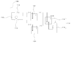
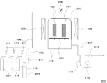
- FIG. 7 is a cross-sectional view showing the configuration of the vapor phase growth apparatus 200 in the third embodiment.
- the vapor phase growth apparatus 200 supplies a first source gas containing gallium and a second source gas containing ammonia to the substrate 201 in the reaction vessel 203, and the general formula Al x In is formed on the substrate 201.
- This is a device for growing a nitride semiconductor represented by y Ga 1-xy N (where x and y are 0 ⁇ x ⁇ 1, 0 ⁇ y ⁇ 1, and 0 ⁇ x + y ⁇ 1).
- the vapor phase growth apparatus 200 includes a reaction tank 203, a substrate holding unit 202, a gas introduction pipe 204, a capturing unit 217, and a gas discharge pipe 205.
- a first source gas containing gallium or a second source gas containing ammonia can be supplied toward the substrate 201.
- a halogen-containing gas can be introduced into the reaction vessel 203, and contaminants attached from various parts in the vapor phase growth apparatus 200 can be removed. The removed contaminant can be discharged from the gas discharge pipe 205.
- the vapor phase growth apparatus 200 is provided with a heating device 206 for heating the inside of the reaction vessel 203 and a pressure gauge 208 for monitoring the pressure inside the reaction vessel 203 around the reaction vessel 203. Can do.
- the reaction vessel 203 is not particularly limited, but is formed of a heat resistant material such as quartz.
- a substrate holding unit 202 is disposed inside the reaction vessel 203, and a substrate 201 for growing a nitride semiconductor is disposed on the substrate holding unit 202.
- the shape and size of the reaction tank 203 are not particularly limited, but can be appropriately determined depending on the size and processing amount of the substrate 201.
- the capturing means 217 plays a role of capturing a reaction product generated by a reaction between a contaminant such as GaN and a halogen-containing gas.
- a contaminant such as GaN
- a halogen-containing gas is introduced into the reaction tank 203 through the gas introduction pipe 204 to clean various components in the reaction tank 203. This is performed in the vapor phase growth apparatus 200.
- the capturing means 217 plays a role of capturing a reaction product of the halogen-containing gas and the contaminant. Since the reaction product is captured by the capturing means 217, it is possible to suppress the reaction product from adhering to other parts and the like, and it is possible to efficiently remove the adhered contaminants. Therefore, the vapor phase growth apparatus 200 provided with the capturing means 217 does not need to remove and clean the parts once contaminated, and can manufacture a nitride semiconductor with a high yield.
- the vapor phase growth apparatus 200 further includes a cooling unit 219 for cooling the capturing unit 217, a substrate holding unit 202 is disposed inside the reaction vessel 203, and trapping is performed inside the cooling unit 219. It is more preferable to adopt a configuration in which the means 217 is arranged. By adopting such a configuration, it is possible to clearly separate the cleaning process of the components in the vapor phase growth apparatus 200 and the capture of the reaction product. Furthermore, since the cooling of the reaction product captured by the capturing unit 217 can be cooled by the cooling unit 219 and the reaction product can be precipitated, the reaction product adheres to the components in the vapor phase growth apparatus 200. Can be further suppressed, and the reaction product can be captured more efficiently.
- the capturing means 217 is not particularly limited as long as it can capture the reaction product, but a cooling panel is preferable. By using the cooling panel, the vapor of the reaction product can be efficiently cooled, so that the reaction product can be captured more efficiently.
- the capturing means 217 is not particularly limited, but is preferably formed from a material that does not react with the reaction product, such as carbon, quartz, stainless steel, hastelloy, silicon carbide, silicon nitride, boron nitride. Quartz is particularly preferable because of its excellent heat resistance.
- the reaction here refers to an irreversible reaction such as corrosion. However, it does not include cases where it is simply deposited or adsorbed.
- the cooling unit 219 has a function of adjusting the temperature inside the capturing unit 217. After capturing the reaction product by lowering the temperature, the trapped reaction product can be re-vaporized by switching to a higher temperature. Therefore, the reaction product can be discharged from the gas discharge pipe 205 more efficiently.
- the function of adjusting the temperature inside the capturing means 217 described above includes, for example, the temperature control fluid circulator 220.
- the cooling unit 219 By flowing the cooling water from the temperature control fluid circulator 220 to the cooling unit 219, the cooling unit 219 can be lowered.
- the cooling unit By flowing oil from the temperature controlled fluid circulator 220, the cooling unit can be heated to a high temperature.
- the temperature of the cooling water for cooling the cooling unit 219 is preferably 0 ° C. or higher and 40 ° C. or lower.
- the temperature of the oil that warms the cooling unit 219 is preferably 80 ° C. or higher and 200 ° C. or lower.
- the substrate holding part 202 is a member for holding the substrate 201, and is formed of a heat resistant material such as carbon or quartz.
- the substrate holding unit 202 is configured to support the substrate 201 and to hold the state.
- the first source gas containing gallium and the second source gas containing ammonia are supplied from the first source gas generation chamber 223 and the container 218 filled with the second source gas through the gas introduction pipe 204 to the reaction vessel 203. Introduced inside. At this time, the introduction amounts of the first source gas and the second source gas can be adjusted by the gas introduction valve 211. *
- the halogen-containing gas is introduced into the reaction vessel 203 from the container 210 filled with the halogen-containing gas through the gas introduction pipe 204. Further, if necessary, the concentration of the halogen-containing gas can be adjusted by introducing the inert gas from the container 222 filled with the inert gas together with the introduction of the halogen-containing gas. At this time, the introduction amounts of the halogen-containing gas and the inert gas can be adjusted by the gas introduction valve 211.
- One port of the gas introduction pipe 204 is connected to the reaction tank 203, and the other port is a container 210 filled with a halogen-containing gas, a first source gas generation chamber 223, a container 218 filled with a second source gas, It is connected to a container 222 filled with an inert gas.
- the gas discharge pipe 205 is connected to the vacuum pump 213 via the gas discharge valve 212, whereby the inside of the reaction tank 203 can be in a reduced pressure state. Further, the gas discharge pipe 205 and the vacuum pump 213 can be connected to an exhaust gas abatement treatment apparatus (not shown) as necessary, detoxify the reaction product discharged from the reaction tank 203 and discharge it to the atmosphere. Can do.
- connection part of the gas introduction pipe 204 connected to the upper part of the reaction tank 203, but it may be the side part or the lower part of the reaction tank 203, and the connection part is not particularly limited.
- the number of the gas introduction pipes 204 is one for each gas is shown, the number of the gas introduction pipes 204 is not necessarily one, and a dedicated gas introduction pipe may be provided for each gas.
- a common gas introduction pipe may be used as shown in FIGS.
- connection location of the gas discharge pipe 205 is not particularly limited, but is preferably connected to the capturing means 217 as shown in FIGS. By such connection, the reaction product captured by the capturing means 217 can be efficiently discharged.
- the heating device 206 is not particularly limited, but includes, for example, a heating unit that can heat the inside of the reaction vessel 203 and a temperature regulator that can maintain the inside of the reaction vessel 203 at a constant temperature by adjusting the output of the heating unit. Composed.
- the heating means is not particularly limited, and any known heating means such as a heating wire or lamp heating can be used, and any means capable of heating the inside of the vapor phase growth apparatus 200 may be used.
- the vapor phase growth apparatus 200 may further include a recovery unit 214 that recovers the gallium compound from the discharged reaction product.
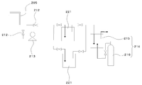
- the recovery unit 214 includes, for example, a recovery unit 215 connected to the gas discharge pipe 205 and a container 216 filled with ammonia so that the discharged reaction product is captured inside the recovery unit 215. It has become. Further, the recovery unit 215 is connected to the container 216, whereby ammonia can be introduced into the recovery unit 215.
- the recovery unit 215 is not particularly limited, but is made of a material having heat resistance and corrosion resistance to a halogen-containing gas, such as carbon, quartz, stainless steel, hastelloy, carbon nitride, silicon nitride, boron nitride, and boron nitride. Yes.
- the recovery unit 215 is provided with, for example, an introduction port through which a reaction product can be introduced, an introduction port through which ammonia can be introduced, and an exhaust port through which exhaust gas can be discharged.
- the vapor phase growth apparatus 200 may be provided with a plurality of traps 221 between the gas discharge pipe 205 and the recovery unit 215.
- the trap 221 can store the reaction product discharged from the gas discharge pipe 205.
- the distance from the gas discharge pipe 205 to the trap 221 or the recovery unit 215 is short. By shortening the distance, the distance in which the vapor of the reaction product diffuses can be shortened, and precipitation in the middle can be further suppressed.
- the vapor phase growth apparatus 200 Mainly, it consists of the manufacture of a nitride semiconductor and a cleaning operation for removing contaminants attached to various components in the vapor phase growth apparatus 200.
- a vapor phase growth method in particular, a MOCVD (Metal Organic Chemical Deposition) method or an HVPE (Hydride Vapor Phase Epitaxy) method is generally used. ing.
- a nitride semiconductor layer is grown on the substrate 201 using a general MOCVD method or HVPE method.
- the substrate 201 is placed in the reaction tank 203, and the temperature in the reaction tank 203 is raised to a certain temperature.
- the first source gas containing gallium is introduced into the reaction vessel 203 through the gas introduction pipe 204 from the first source gas generation chamber 223.
- the first source gas generation chamber 223 will be described.
- the first source gas generation chamber 223 is connected to a container 209 filled with a halogen-containing gas, and includes a source boat that stores Ga therein.
- the halogen-containing gas is introduced into the first source gas generation chamber 223, the source Ga and the halogen-containing gas react to generate a first source gas such as GaCl.
- the halogen-containing gas filled in the container 210 is, for example, Cl 2 , HCl, SiCl 4 , SiHCl 3 , SiH 2 Cl 2 , SiH 3 Cl, BCl 3 , CHCl 3 , CH 2 Cl 2 , CH 3 Cl, or the like.
- Cl 2 is particularly preferable from the viewpoint of price, reactivity and the like.
- the second source gas containing ammonia filled in the container 218 is introduced into the reaction vessel 203.
- GaCl as the first source gas and ammonia as the second source gas react to generate GaN, hydrogen chloride, and hydrogen, and GaN grows on the substrate 201 as a nitride semiconductor layer.
- Hydrogen chloride and hydrogen are discharged as exhaust gas, and hydrogen chloride harmful to the human body is removed by an abatement apparatus not shown.
- the method for forming the nitride semiconductor layer is not limited to the HVPE method described above, and other methods may be used.
- cleaning operation a cleaning operation for removing contaminants attached to various components in the vapor deposition apparatus 200
- the cleaning operation for removing contaminants by the vapor deposition apparatus 200 is not limited thereto.
- the substrate 201 on which the nitride semiconductor layer is formed is taken out from the reaction vessel 203, and the inside of the reaction vessel 203 is heated to a desired temperature, which will be described later, by a heating device 206 as necessary.
- the inside of the reaction vessel 203 may be further depressurized by the vacuum pump 213.
- the pressure inside the reaction vessel 203 is preferably 1 kPa or less, and particularly preferably 0.1 kPa or less.
- the amount is not more than the above upper limit value, the amount of the halogen-containing gas to be introduced can be increased, and at the same time, side reactions caused by undesirable residual gas can be suppressed, and the reaction product can be removed more efficiently.
- the inside of the reaction vessel 203 may be heated after being reduced in pressure, or the heating operation and the pressure reducing operation may be performed simultaneously. The above temperature and pressure may be finally reached, and the order of the heating operation and the decompression operation is not particularly limited.
- the gas introduction valve 211 is opened to introduce a halogen-containing gas into the reaction tank 203.
- the halogen-containing gas is, for example, a compound containing chlorine in a molecule such as Cl 2 , HCl, SiCl 4 , SiHCl 3 , SiH 2 Cl 2 , SiH 3 Cl, BCl 3 , CHCl 3 , CH 2 Cl 2 , and CH 3 Cl.
- Cl 2 is particularly preferable from the viewpoint of price, reactivity and the like.
- the inert gas may introduce
- the concentration of the halogen-containing gas can be adjusted.
- the inert gas for example, one gas or a mixed gas of two or more gases that do not react with a halogen-containing gas such as nitrogen, helium, or argon is used.
- the concentration of the halogen-containing gas in the reaction tank 203 when the above inert gas is introduced is not particularly limited, but if the concentration is too high, various components in the vapor phase growth apparatus 200 may be corroded. It is set appropriately depending on the degree of contamination.
- the concentration of the halogen-containing gas in the reaction vessel 203 when the inert gas is introduced is not particularly limited, but is preferably 5% by volume or more, and particularly preferably 10% by volume or more. When the value is equal to or higher than the lower limit, the reaction rate between the contaminants and the halogen-containing gas is increased, and contaminants attached to various components in the vapor phase growth apparatus 200 can be more efficiently removed.
- the concentration of the halogen-containing gas is not particularly limited, but is preferably 100% by volume or less, particularly preferably 80% by volume or less. When the amount is not more than the above upper limit value, the halogen-containing gas amount can be reduced, and corrosion of the device components can be suppressed.
- This reaction product immediately evaporates into a vapor and drifts inside the reaction vessel 203 and the trapping means 217.
- the gas introduction valve 211 and the gas discharge valve 212 are closed to hold the halogen-containing gas in the apparatus so that the halogen-containing gas reacts with contaminants.
- the gas introduction valve 211 and the gas discharge valve 212 may not be completely closed.
- the gas introduction valve 211 is closed, and the halogen-containing gas is kept constant in the reaction tank 203 and the capturing means 217. Hold for hours.
- the internal pressure of the reaction vessel 203 is preferably 10 kPa or more, and particularly preferably 12 kPa or more.
- the internal pressure is preferably 90 kPa or less, and particularly preferably 85 kPa or less.
- the internal pressure is not more than the above upper limit value, the average free process of the reaction product can be lengthened, so that the diffusion efficiency of the reaction product is increased, and the reaction efficiency between the contaminant and the halogen-containing gas can be further increased.
- the internal temperature of the reaction vessel 203 at this time is not particularly limited, but is preferably 500 ° C. or higher, and particularly preferably 750 ° C. or higher.
- the internal temperature is not particularly limited, but is preferably 1000 ° C. or less, and particularly preferably 800 ° C. or less.
- the internal temperature is set to the upper limit value or less, thermal deformation of various components in the vapor phase growth apparatus 200 can be further prevented.
- the holding time of the halogen-containing gas is not particularly limited, but is appropriately set depending on the size of the reaction tank 203, the processing amount of various components in the vapor phase growth apparatus 200, and the like.
- the reaction product generated by the reaction between the halogen-containing gas and the contaminant is captured by the capturing means 217.
- water is allowed to flow from the temperature control fluid circulator 220 to the cooling unit 219 to cool the capturing unit 217. Then, the vapor of the reaction product is cooled inside the trapping means 217 and deposited on the surface of the trapping means 217 and trapped.
- the gas discharge valve 212 is opened, and exhaust gas such as unreacted halogen-containing gas or untrapped gas is discharged from the gas discharge pipe 205.
- the gas introduction pipe 204 it is more preferable to open the gas introduction pipe 204, introduce an inert gas from the vessel 210 to the reaction vessel 203, return the inside of the reaction vessel 203 to atmospheric pressure, and then exhaust the exhaust gas.
- the inert gas used at this time is not particularly limited, but the above-described inert gas may be used, or another gas may be used.
- the cleaning operation of various components in the vapor phase growth apparatus 200 using the vapor phase growth apparatus 200 in the third embodiment is performed twice or more from the introduction of the halogen-containing gas to the discharge of the exhaust gas. Is preferred.
- the surfaces of various parts are further activated, and the reaction efficiency between the contaminants and the halogen-containing gas can be further increased.
- the number of repetitions is not particularly limited, but is appropriately set depending on the size of the reaction tank 203, the processing amount of various components, and the like.
- the cleaning operation of various components in the vapor phase growth apparatus 200 using the vapor phase growth apparatus 200 in the third embodiment further discharges the captured reaction product.
- the method for discharging the reaction product is not particularly limited. For example, high temperature oil is allowed to flow from the temperature control fluid circulator 220 to the cooling unit 219, and the trapping means 217 is warmed. Then, the reaction product deposited on the surface of the capturing means 217 becomes steam again and is discharged from the gas discharge pipe 205.
- the gas introduction pipe 204 it is more preferable to open the gas introduction pipe 204, introduce an inert gas from the vessel 210 to the reaction vessel 203, return the inside of the reaction vessel 203 to atmospheric pressure, and then discharge the vapor of the reaction product. .
- the inert gas By introducing the inert gas, the vapor of the reaction product is pushed out by the inert gas, and the vapor can be discharged more efficiently.
- the inert gas used at this time is not particularly limited, but the above-described inert gas may be used, or another gas may be used.
- the cleaning operation of various components in the vapor phase growth apparatus 200 using the vapor phase growth apparatus 200 in the third embodiment is performed after the reaction product captured by the capture unit 217 is accumulated in a certain amount and then captured. It is preferable to discharge the reaction product.
- the number of repetitions is not particularly limited, but is appropriately set depending on the amount of reaction product trapped.
- the cleaning operation of various components in the vapor phase growth apparatus 200 using the vapor phase growth apparatus 200 in the third embodiment further recovers the gallium compound from the reaction product.
- the recovery method is not particularly limited, but can be performed using, for example, an apparatus as shown in FIG.
- the vapor of the reaction product discharged from the gas discharge pipe 205 is captured by the recovery unit 215.
- ammonia gas is introduced from the container 216 to the recovery unit 215, and gallium halide and the like contained in the reaction product are reacted with ammonia to generate a solid such as a gallium compound.
- the vapor phase growth apparatus 200 captures and accumulates a certain amount of reaction products discharged to the plurality of traps 221 between the gas discharge pipe 205 and the recovery unit 215.
- the reaction product may be sent to the recovery unit 215.
- the growth by the HVPE method is taken as an example, but the present invention can also be applied to an MOCVD method, an atomic layer deposition method (ALD), or the like.
- Example 1 Hereinafter, in Examples 1 to 7 and Comparative Examples 1 and 2, the cleaning apparatus shown in FIG. 1 was used.
- the semiconductor manufacturing apparatus component to which GaN was adhered was placed in the component holder in the reaction vessel, the temperature in the reaction vessel was set to 750 ° C., and the pressure was set to 0.1 kPa or less.
- N 2 gas was introduced into the reaction tank to a pressure of 20 kPa, and then Cl 2 gas was introduced into the reaction tank to a pressure of 40 kPa (Cl 2 gas pressure was 20 kPa).
- the exhaust valve was opened and the vapor of the reaction product was discharged.
- reaction efficiency 100 ⁇ (number of moles of GaN removed ⁇ 1.5) / (number of moles of Cl 2 used) (1)
- the amount of Cl 2 gas required to remove 1 mol of GaN is theoretically 1.5 mol.
- the removed GaN was 3.5 g (0.042 mol), and the total amount of Cl 2 gas used was 3.2 L (0.13 mol). Therefore, the reaction efficiency was 48.2%.
- Example 2 The same cleaning treatment as in Example 1 was performed except that the series of operations of introducing the N 2 gas, introducing the Cl 2 gas, holding for 10 minutes, and discharging the reaction product was performed four times. The obtained results are shown in Table 1.
- Example 3 The semiconductor manufacturing apparatus component to which GaN adhered was placed in the component holding part in the reaction vessel, the temperature in the reaction vessel was set to 730 ° C., and the pressure was set to 0.1 kPa or less. Next, N 2 gas was introduced into the reaction tank to a pressure of 10 kPa, and then Cl 2 gas was introduced into the reaction tank to a pressure of 30 kPa. After maintaining for 10 minutes, the exhaust valve was opened and the vapor of the reaction product was discharged. Subsequently, the series of operations of introducing the N 2 gas, introducing the Cl 2 gas, holding for 10 minutes, and discharging the reaction product was performed twice.
- Examples 4 to 7, Comparative Example 1 The same cleaning treatment as in Example 3 was performed except that the pressure in the reaction vessel was set to the values described in Table 1, respectively. The obtained results are shown in Table 1.
- Example 8 Hereinafter, in Example 8, the cleaning apparatus shown in FIGS. 4 and 5 was used.
- the semiconductor manufacturing apparatus component to which GaN adhered was placed in the component holding unit in the cleaning processing unit, and the temperature in the cleaning processing unit was set to 750 ° C. Further, water having a water temperature of 25 ° C. was circulated to the cooling unit at 2 L / min by a temperature control fluid circulator. Thereafter, the vacuum pump was operated, and the pressure in the cleaning processing unit was set to 0.1 kPa or less. Next, N 2 gas was introduced into the cleaning treatment section to make the pressure 20 kPa, and then Cl 2 gas was introduced into the reaction tank to make the pressure 40 kPa.
- the exhaust valve was opened to exhaust the exhaust gas.
- the above series of operations of introducing N 2 gas, introducing Cl 2 gas, holding for 10 minutes, and discharging exhaust gas were performed a total of 4 times.
- 100 degreeC oil was circulated to the cooling part at 3 L / min with the temperature control fluid circulator, and the cooling panel in a cooling part was warmed.
- the gas exhaust valve was opened, and the vapor of the reaction product, GaCl 3 , was introduced into the recovery unit.
- NH 3 gas was introduced into the recovery unit to react GaCl 3 and NH 3 .
- reaction efficiency 100 ⁇ (number of moles of GaN removed ⁇ 1.5) / (number of moles of Cl 2 used) (1)
- the amount of Cl 2 gas required to remove 1 mol of GaN is theoretically 1.5 mol.
- the removed GaN was 28.1 g (0.336 mol), and the total amount of Cl 2 gas used was 12.8 L (0.520 mol). Therefore, the reaction efficiency was 96.9%.
- gallium compounds such as oligomers (NH 2 GaCl 2 ) n and GaN containing NH 4 Cl and Ga were captured from the recovery unit.
Landscapes
- Chemical & Material Sciences (AREA)
- General Chemical & Material Sciences (AREA)
- Chemical Kinetics & Catalysis (AREA)
- Engineering & Computer Science (AREA)
- Materials Engineering (AREA)
- Mechanical Engineering (AREA)
- Metallurgy (AREA)
- Organic Chemistry (AREA)
- Chemical Vapour Deposition (AREA)
- Cleaning Or Drying Semiconductors (AREA)
- Drying Of Semiconductors (AREA)
Abstract
Priority Applications (7)
| Application Number | Priority Date | Filing Date | Title |
|---|---|---|---|
| KR1020157010082A KR20150048914A (ko) | 2011-05-19 | 2012-03-15 | 반도체 제조장치부품의 세정방법, 반도체 제조장치부품의 세정장치 및 기상성장장치 |
| EP12784871.1A EP2711974A4 (fr) | 2011-05-19 | 2012-03-15 | Procédé de lavage de composants d'un appareil de fabrication de semi-conducteurs, appareil de lavage d'un composant d'un appareil de fabrication de semi-conducteurs, et appareil de croissance en phase vapeur |
| CN201280024377.XA CN103597583B (zh) | 2011-05-19 | 2012-03-15 | 半导体制造装置部件的清洗方法、半导体制造装置部件的清洗装置及气相生长装置 |
| KR1020137033710A KR101553458B1 (ko) | 2011-05-19 | 2012-03-15 | 반도체 제조장치부품의 세정방법, 반도체 제조장치부품의 세정장치 및 기상성장장치 |
| US14/116,037 US20140144381A1 (en) | 2011-05-19 | 2012-03-15 | Method for washing semiconductor manufacturing apparatus component, apparatus for washing semiconductor manufacturing apparatus component, and vapor phase growth apparatus |
| JP2013514961A JP5715245B2 (ja) | 2011-05-19 | 2012-03-15 | 半導体製造装置部品の洗浄装置および気相成長装置 |
| US16/223,689 US10741380B2 (en) | 2011-05-19 | 2018-12-18 | Method for washing semiconductor manufacturing apparatus component, apparatus for washing semiconductor manufacturing apparatus component, and vapor phase growth apparatus |
Applications Claiming Priority (4)
| Application Number | Priority Date | Filing Date | Title |
|---|---|---|---|
| JP2011112426 | 2011-05-19 | ||
| JP2011-112426 | 2011-05-19 | ||
| JP2011-162261 | 2011-07-25 | ||
| JP2011162261 | 2011-07-25 |
Related Child Applications (2)
| Application Number | Title | Priority Date | Filing Date |
|---|---|---|---|
| US14/116,037 A-371-Of-International US20140144381A1 (en) | 2011-05-19 | 2012-03-15 | Method for washing semiconductor manufacturing apparatus component, apparatus for washing semiconductor manufacturing apparatus component, and vapor phase growth apparatus |
| US16/223,689 Division US10741380B2 (en) | 2011-05-19 | 2018-12-18 | Method for washing semiconductor manufacturing apparatus component, apparatus for washing semiconductor manufacturing apparatus component, and vapor phase growth apparatus |
Publications (1)
| Publication Number | Publication Date |
|---|---|
| WO2012157161A1 true WO2012157161A1 (fr) | 2012-11-22 |
Family
ID=47176517
Family Applications (1)
| Application Number | Title | Priority Date | Filing Date |
|---|---|---|---|
| PCT/JP2012/001829 Ceased WO2012157161A1 (fr) | 2011-05-19 | 2012-03-15 | Procédé de lavage de composants d'un appareil de fabrication de semi-conducteurs, appareil de lavage d'un composant d'un appareil de fabrication de semi-conducteurs, et appareil de croissance en phase vapeur |
Country Status (7)
| Country | Link |
|---|---|
| US (2) | US20140144381A1 (fr) |
| EP (1) | EP2711974A4 (fr) |
| JP (2) | JP5715245B2 (fr) |
| KR (2) | KR20150048914A (fr) |
| CN (1) | CN103597583B (fr) |
| TW (2) | TWI482213B (fr) |
| WO (1) | WO2012157161A1 (fr) |
Cited By (1)
| Publication number | Priority date | Publication date | Assignee | Title |
|---|---|---|---|---|
| JP2016201481A (ja) * | 2015-04-10 | 2016-12-01 | 株式会社ニューフレアテクノロジー | 気相成長方法 |
Families Citing this family (3)
| Publication number | Priority date | Publication date | Assignee | Title |
|---|---|---|---|---|
| JP6679413B2 (ja) * | 2016-05-23 | 2020-04-15 | 大陽日酸株式会社 | 気相成長装置用部品の洗浄装置 |
| JP6852040B2 (ja) | 2018-11-16 | 2021-03-31 | 大陽日酸株式会社 | 半導体製造装置部品の洗浄装置、半導体製造装置部品の洗浄方法、及び半導体製造装置部品の洗浄システム |
| KR102209540B1 (ko) | 2020-08-03 | 2021-01-29 | 씨에스이(주) | 밸브 세정장치 |
Citations (10)
| Publication number | Priority date | Publication date | Assignee | Title |
|---|---|---|---|---|
| JPS6465023A (en) * | 1987-05-06 | 1989-03-10 | Rhone Poulenc Chimie | Collection of gallium from liquid liquid extraction |
| JP2006332201A (ja) | 2005-05-24 | 2006-12-07 | Taiyo Nippon Sanso Corp | 窒化物半導体製造装置の洗浄方法と洗浄装置 |
| JP2007109928A (ja) | 2005-10-14 | 2007-04-26 | Taiyo Nippon Sanso Corp | 窒化物半導体製造装置部品の洗浄方法と洗浄装置 |
| JP2009124050A (ja) * | 2007-11-16 | 2009-06-04 | Hitachi Kokusai Electric Inc | 半導体装置の製造方法及び基板処理装置 |
| JP2009188198A (ja) * | 2008-02-06 | 2009-08-20 | Taiyo Nippon Sanso Corp | 半導体装置の製造方法及び基板処理装置 |
| JP2010016200A (ja) * | 2008-07-03 | 2010-01-21 | Zeta Photon Kk | シャドーマスクのクリーニング方法、シャドーマスクのクリーニング装置、有機elディスプレイの製造方法および有機elディスプレイの製造装置 |
| JP2010212400A (ja) | 2009-03-10 | 2010-09-24 | Taiyo Nippon Sanso Corp | 窒化物半導体製造装置部品の洗浄方法及び洗浄装置 |
| JP2010245376A (ja) | 2009-04-08 | 2010-10-28 | Taiyo Nippon Sanso Corp | 窒化物半導体製造装置における汚染部品の洗浄装置 |
| JP2011112426A (ja) | 2009-11-25 | 2011-06-09 | Yokogawa Electric Corp | ペーパーレスレコーダ |
| JP2011162261A (ja) | 2010-02-08 | 2011-08-25 | Katsuyoshi Fukuyama | 内圧排出構造の包装袋 |
Family Cites Families (24)
| Publication number | Priority date | Publication date | Assignee | Title |
|---|---|---|---|---|
| US4551197A (en) * | 1984-07-26 | 1985-11-05 | Guilmette Joseph G | Method and apparatus for the recovery and recycling of condensable gas reactants |
| JPH1180964A (ja) * | 1997-07-07 | 1999-03-26 | Canon Inc | プラズマcvd法による堆積膜形成装置 |
| JP3554219B2 (ja) * | 1998-03-31 | 2004-08-18 | キヤノン株式会社 | 排気装置と排気方法、および堆積膜形成装置と堆積膜形成方法 |
| JP2963443B1 (ja) * | 1998-06-19 | 1999-10-18 | キヤノン販売株式会社 | 半導体装置の製造装置 |
| US6238514B1 (en) * | 1999-02-18 | 2001-05-29 | Mks Instruments, Inc. | Apparatus and method for removing condensable aluminum vapor from aluminum etch effluent |
| US6773687B1 (en) * | 1999-11-24 | 2004-08-10 | Tokyo Electron Limited | Exhaust apparatus for process apparatus and method of removing impurity gas |
| US6770145B2 (en) * | 2000-12-11 | 2004-08-03 | Tanaka Kikinzoku Kogyo K.K. | Low-pressure CVD apparatus and method of manufacturing a thin film |
| JP4679720B2 (ja) * | 2000-12-22 | 2011-04-27 | 東京エレクトロン株式会社 | 処理装置 |
| US20030196680A1 (en) * | 2002-04-19 | 2003-10-23 | Dielectric Systems, Inc | Process modules for transport polymerization of low epsilon thin films |
| US6902623B2 (en) * | 2001-06-07 | 2005-06-07 | Veeco Instruments Inc. | Reactor having a movable shutter |
| US6847905B2 (en) * | 2002-02-12 | 2005-01-25 | Tektronix, Inc. | Architecture providing increased information display for long acquisitions or constrained memory bandwidth |
| US20030216041A1 (en) | 2002-05-08 | 2003-11-20 | Herring Robert B. | In-situ thermal chamber cleaning |
| US7074298B2 (en) * | 2002-05-17 | 2006-07-11 | Applied Materials | High density plasma CVD chamber |
| KR100513276B1 (ko) * | 2003-05-23 | 2005-09-09 | 삼성전자주식회사 | 웨이퍼 고정 스핀 척 |
| TWI250669B (en) | 2003-11-26 | 2006-03-01 | Sanken Electric Co Ltd | Semiconductor light emitting element and its manufacturing method |
| US7455720B2 (en) * | 2005-02-16 | 2008-11-25 | Mks Instruments, Inc. | Method and apparatus for preventing products of TiCL4 and NH3 or other feed gas reactions from damaging vacuum pumps in TiN or other deposition systems |
| CN2808933Y (zh) * | 2005-05-12 | 2006-08-23 | 应用材料公司 | 远程等离子反应器的并合器 |
| KR100621660B1 (ko) * | 2005-07-01 | 2006-09-11 | 주식회사 뉴프로텍 | 반도체 부산물 트랩장치 |
| KR101379410B1 (ko) | 2006-11-22 | 2014-04-11 | 소이텍 | 3-5족 반도체 재료들의 대량생산을 위한 설비 |
| DE102008039430A1 (de) * | 2007-08-23 | 2009-02-26 | Von Ardenne Anlagentechnik Gmbh | Durchlaufbeschichtungsanlage |
| JP5260356B2 (ja) * | 2009-03-05 | 2013-08-14 | 東京エレクトロン株式会社 | 基板処理方法 |
| US20110079251A1 (en) * | 2009-04-28 | 2011-04-07 | Olga Kryliouk | Method for in-situ cleaning of deposition systems |
| US20100273291A1 (en) * | 2009-04-28 | 2010-10-28 | Applied Materials, Inc. | Decontamination of mocvd chamber using nh3 purge after in-situ cleaning |
| WO2011031521A2 (fr) * | 2009-08-27 | 2011-03-17 | Applied Materials, Inc. | Procédé de décontamination d'une chambre de traitement après nettoyage de la chambre in situ |
-
2012
- 2012-03-15 KR KR1020157010082A patent/KR20150048914A/ko not_active Ceased
- 2012-03-15 US US14/116,037 patent/US20140144381A1/en not_active Abandoned
- 2012-03-15 CN CN201280024377.XA patent/CN103597583B/zh not_active Expired - Fee Related
- 2012-03-15 KR KR1020137033710A patent/KR101553458B1/ko not_active Expired - Fee Related
- 2012-03-15 WO PCT/JP2012/001829 patent/WO2012157161A1/fr not_active Ceased
- 2012-03-15 EP EP12784871.1A patent/EP2711974A4/fr not_active Withdrawn
- 2012-03-15 JP JP2013514961A patent/JP5715245B2/ja not_active Expired - Fee Related
- 2012-03-21 TW TW101109737A patent/TWI482213B/zh not_active IP Right Cessation
- 2012-03-21 TW TW104102429A patent/TWI552213B/zh not_active IP Right Cessation
-
2015
- 2015-01-05 JP JP2015000470A patent/JP2015073132A/ja active Pending
-
2018
- 2018-12-18 US US16/223,689 patent/US10741380B2/en not_active Expired - Fee Related
Patent Citations (10)
| Publication number | Priority date | Publication date | Assignee | Title |
|---|---|---|---|---|
| JPS6465023A (en) * | 1987-05-06 | 1989-03-10 | Rhone Poulenc Chimie | Collection of gallium from liquid liquid extraction |
| JP2006332201A (ja) | 2005-05-24 | 2006-12-07 | Taiyo Nippon Sanso Corp | 窒化物半導体製造装置の洗浄方法と洗浄装置 |
| JP2007109928A (ja) | 2005-10-14 | 2007-04-26 | Taiyo Nippon Sanso Corp | 窒化物半導体製造装置部品の洗浄方法と洗浄装置 |
| JP2009124050A (ja) * | 2007-11-16 | 2009-06-04 | Hitachi Kokusai Electric Inc | 半導体装置の製造方法及び基板処理装置 |
| JP2009188198A (ja) * | 2008-02-06 | 2009-08-20 | Taiyo Nippon Sanso Corp | 半導体装置の製造方法及び基板処理装置 |
| JP2010016200A (ja) * | 2008-07-03 | 2010-01-21 | Zeta Photon Kk | シャドーマスクのクリーニング方法、シャドーマスクのクリーニング装置、有機elディスプレイの製造方法および有機elディスプレイの製造装置 |
| JP2010212400A (ja) | 2009-03-10 | 2010-09-24 | Taiyo Nippon Sanso Corp | 窒化物半導体製造装置部品の洗浄方法及び洗浄装置 |
| JP2010245376A (ja) | 2009-04-08 | 2010-10-28 | Taiyo Nippon Sanso Corp | 窒化物半導体製造装置における汚染部品の洗浄装置 |
| JP2011112426A (ja) | 2009-11-25 | 2011-06-09 | Yokogawa Electric Corp | ペーパーレスレコーダ |
| JP2011162261A (ja) | 2010-02-08 | 2011-08-25 | Katsuyoshi Fukuyama | 内圧排出構造の包装袋 |
Non-Patent Citations (1)
| Title |
|---|
| See also references of EP2711974A4 |
Cited By (1)
| Publication number | Priority date | Publication date | Assignee | Title |
|---|---|---|---|---|
| JP2016201481A (ja) * | 2015-04-10 | 2016-12-01 | 株式会社ニューフレアテクノロジー | 気相成長方法 |
Also Published As
| Publication number | Publication date |
|---|---|
| TW201519294A (zh) | 2015-05-16 |
| TWI552213B (zh) | 2016-10-01 |
| US20140144381A1 (en) | 2014-05-29 |
| CN103597583A (zh) | 2014-02-19 |
| TWI482213B (zh) | 2015-04-21 |
| KR20140010459A (ko) | 2014-01-24 |
| JPWO2012157161A1 (ja) | 2014-07-31 |
| EP2711974A1 (fr) | 2014-03-26 |
| KR101553458B1 (ko) | 2015-09-15 |
| JP5715245B2 (ja) | 2015-05-07 |
| TW201248704A (en) | 2012-12-01 |
| US20190122880A1 (en) | 2019-04-25 |
| KR20150048914A (ko) | 2015-05-07 |
| US10741380B2 (en) | 2020-08-11 |
| CN103597583B (zh) | 2016-06-08 |
| JP2015073132A (ja) | 2015-04-16 |
| EP2711974A4 (fr) | 2015-03-11 |
Similar Documents
| Publication | Publication Date | Title |
|---|---|---|
| JP6463339B2 (ja) | 後続の多段洗浄ステップを伴うmocvd層成長方法 | |
| US6844273B2 (en) | Precleaning method of precleaning a silicon nitride film forming system | |
| CN1992168B (zh) | 第iii族氮化物晶体物质的制造方法和制造装置 | |
| TWI496935B (zh) | Mocvd腔室在原位清潔後利用nh3淨化之去汙染 | |
| US20120304930A1 (en) | Chamber exhaust in-situ cleaning for processing apparatuses | |
| TW201101531A (en) | MOCVD single chamber split process for LED manufacturing | |
| JP5877702B2 (ja) | 成膜装置および成膜方法 | |
| WO2002101805A1 (fr) | Procede de nettoyage d'un appareil de formation de film mince | |
| US10741380B2 (en) | Method for washing semiconductor manufacturing apparatus component, apparatus for washing semiconductor manufacturing apparatus component, and vapor phase growth apparatus | |
| CN102899635A (zh) | 一种原位清洁mocvd反应腔室的方法 | |
| WO2010129289A4 (fr) | Décontamination d'une chambre mocvd à l'aide d'une purge au nh3 après un nettoyage in situ | |
| KR101909430B1 (ko) | 반도체 공정 시스템용 가스 파우더처리 장치 및 방법 | |
| US20160097144A1 (en) | Contamination control method of vapor deposition apparatus and method of producing epitaxial silicon wafer | |
| JP2001293332A (ja) | Cvd排ガスの処理回収方法及び装置 | |
| KR20130090698A (ko) | 반도체 공정 시스템용 가스 파우더처리 장치 및 방법 | |
| JP2024118350A (ja) | 気相成長装置及び気相成長方法 | |
| KR101518215B1 (ko) | 사용 후 잔류 TMIn 회수 및 정제 시스템 | |
| CN119824530A (zh) | SiC外延生长装置的副产物除去方法 | |
| JP2006108722A (ja) | シリコン窒化膜の形成方法及び形成装置 |
Legal Events
| Date | Code | Title | Description |
|---|---|---|---|
| 121 | Ep: the epo has been informed by wipo that ep was designated in this application |
Ref document number: 12784871 Country of ref document: EP Kind code of ref document: A1 |
|
| ENP | Entry into the national phase |
Ref document number: 2013514961 Country of ref document: JP Kind code of ref document: A |
|
| WWE | Wipo information: entry into national phase |
Ref document number: 14116037 Country of ref document: US |
|
| NENP | Non-entry into the national phase |
Ref country code: DE |
|
| WWE | Wipo information: entry into national phase |
Ref document number: 2012784871 Country of ref document: EP |
|
| ENP | Entry into the national phase |
Ref document number: 20137033710 Country of ref document: KR Kind code of ref document: A |