WO2012157181A1 - パターン検査装置および検査方法 - Google Patents
パターン検査装置および検査方法 Download PDFInfo
- Publication number
- WO2012157181A1 WO2012157181A1 PCT/JP2012/002410 JP2012002410W WO2012157181A1 WO 2012157181 A1 WO2012157181 A1 WO 2012157181A1 JP 2012002410 W JP2012002410 W JP 2012002410W WO 2012157181 A1 WO2012157181 A1 WO 2012157181A1
- Authority
- WO
- WIPO (PCT)
- Prior art keywords
- sample
- result
- inspection apparatus
- pattern
- pattern inspection
- Prior art date
- Legal status (The legal status is an assumption and is not a legal conclusion. Google has not performed a legal analysis and makes no representation as to the accuracy of the status listed.)
- Ceased
Links
Images






Classifications
-
- G—PHYSICS
- G01—MEASURING; TESTING
- G01N—INVESTIGATING OR ANALYSING MATERIALS BY DETERMINING THEIR CHEMICAL OR PHYSICAL PROPERTIES
- G01N23/00—Investigating or analysing materials by the use of wave or particle radiation, e.g. X-rays or neutrons, not covered by groups G01N3/00 – G01N17/00, G01N21/00 or G01N22/00
- G01N23/22—Investigating or analysing materials by the use of wave or particle radiation, e.g. X-rays or neutrons, not covered by groups G01N3/00 – G01N17/00, G01N21/00 or G01N22/00 by measuring secondary emission from the material
- G01N23/225—Investigating or analysing materials by the use of wave or particle radiation, e.g. X-rays or neutrons, not covered by groups G01N3/00 – G01N17/00, G01N21/00 or G01N22/00 by measuring secondary emission from the material using electron or ion
- G01N23/2251—Investigating or analysing materials by the use of wave or particle radiation, e.g. X-rays or neutrons, not covered by groups G01N3/00 – G01N17/00, G01N21/00 or G01N22/00 by measuring secondary emission from the material using electron or ion using incident electron beams, e.g. scanning electron microscopy [SEM]
-
- G—PHYSICS
- G03—PHOTOGRAPHY; CINEMATOGRAPHY; ANALOGOUS TECHNIQUES USING WAVES OTHER THAN OPTICAL WAVES; ELECTROGRAPHY; HOLOGRAPHY
- G03F—PHOTOMECHANICAL PRODUCTION OF TEXTURED OR PATTERNED SURFACES, e.g. FOR PRINTING, FOR PROCESSING OF SEMICONDUCTOR DEVICES; MATERIALS THEREFOR; ORIGINALS THEREFOR; APPARATUS SPECIALLY ADAPTED THEREFOR
- G03F1/00—Originals for photomechanical production of textured or patterned surfaces, e.g., masks, photo-masks, reticles; Mask blanks or pellicles therefor; Containers specially adapted therefor; Preparation thereof
- G03F1/68—Preparation processes not covered by groups G03F1/20 - G03F1/50
- G03F1/82—Auxiliary processes, e.g. cleaning or inspecting
- G03F1/84—Inspecting
- G03F1/86—Inspecting by charged particle beam [CPB]
-
- G—PHYSICS
- G03—PHOTOGRAPHY; CINEMATOGRAPHY; ANALOGOUS TECHNIQUES USING WAVES OTHER THAN OPTICAL WAVES; ELECTROGRAPHY; HOLOGRAPHY
- G03F—PHOTOMECHANICAL PRODUCTION OF TEXTURED OR PATTERNED SURFACES, e.g. FOR PRINTING, FOR PROCESSING OF SEMICONDUCTOR DEVICES; MATERIALS THEREFOR; ORIGINALS THEREFOR; APPARATUS SPECIALLY ADAPTED THEREFOR
- G03F7/00—Photomechanical, e.g. photolithographic, production of textured or patterned surfaces, e.g. printing surfaces; Materials therefor, e.g. comprising photoresists; Apparatus specially adapted therefor
- G03F7/70—Microphotolithographic exposure; Apparatus therefor
- G03F7/70483—Information management; Active and passive control; Testing; Wafer monitoring, e.g. pattern monitoring
- G03F7/70605—Workpiece metrology
- G03F7/70616—Monitoring the printed patterns
- G03F7/7065—Defects, e.g. optical inspection of patterned layer for defects
-
- H—ELECTRICITY
- H10—SEMICONDUCTOR DEVICES; ELECTRIC SOLID-STATE DEVICES NOT OTHERWISE PROVIDED FOR
- H10P—GENERIC PROCESSES OR APPARATUS FOR THE MANUFACTURE OR TREATMENT OF DEVICES COVERED BY CLASS H10
- H10P74/00—Testing or measuring during manufacture or treatment of wafers, substrates or devices
- H10P74/20—Testing or measuring during manufacture or treatment of wafers, substrates or devices characterised by the properties tested or measured, e.g. structural or electrical properties
- H10P74/203—Structural properties, e.g. testing or measuring thicknesses, line widths, warpage, bond strengths or physical defects
-
- G—PHYSICS
- G01—MEASURING; TESTING
- G01N—INVESTIGATING OR ANALYSING MATERIALS BY DETERMINING THEIR CHEMICAL OR PHYSICAL PROPERTIES
- G01N2223/00—Investigating materials by wave or particle radiation
- G01N2223/60—Specific applications or type of materials
- G01N2223/611—Specific applications or type of materials patterned objects; electronic devices
-
- G—PHYSICS
- G01—MEASURING; TESTING
- G01N—INVESTIGATING OR ANALYSING MATERIALS BY DETERMINING THEIR CHEMICAL OR PHYSICAL PROPERTIES
- G01N2223/00—Investigating materials by wave or particle radiation
- G01N2223/60—Specific applications or type of materials
- G01N2223/646—Specific applications or type of materials flaws, defects
Definitions
- the present invention relates to a method and apparatus for manufacturing a substrate having a fine pattern such as a semiconductor device, liquid crystal, photomask, or nanoimprint, and more particularly to a technique for inspecting a semiconductor device and a mask pattern using an electron beam.
- Patent Document 1 Japanese Patent Application Laid-Open No. 2007-059176 discloses a technique for irradiating ultraviolet light for cleaning an observation portion when observing a mask with an electron microscope. Further, in Patent Document 2 (Japanese Patent Laid-Open No. 2007-220471), an on-mask circuit pattern image acquired in advance with a mask electron microscope is displayed simultaneously when an electron beam image is acquired with a wafer electron microscope. Technology is disclosed.
- a pattern necessary for circuit formation is designed by CAD, and this design data is formed on a photomask (reticle). That is, the design pattern shape is formed as a light shielding film on a transparent substrate.
- a circuit pattern is formed on a semiconductor wafer by loading the photomask into a reduction exposure apparatus and exposing and imaging light passing through the photomask on a wafer coated with a photoconductor. Since the reduction ratio of the reduction exposure apparatus is generally 1/4 to 1/5, the pattern on the mask is enlarged 4 to 5 times the pattern on the wafer.
- the pattern formed on the wafer and the pattern formed on the mask are becoming smaller.
- a phase shift method or an OPC technique is used in the mask.
- the EUV lithography further eliminates the protective film of the mask, which may cause foreign matters and defects on the mask during use and handling.
- the substrate is a multilayer film
- defects existing on the mask may not be transferred to the wafer, or defects embedded in the multilayer film and difficult to detect by mask inspection may be transferred onto the wafer.
- a semiconductor device is inspected by an inspection device dedicated to the wafer, and the inspection coordinate data for the wafer is used to observe and measure the dimensions with an electron microscope dedicated to the wafer.
- the same applies to photomasks in which inspection is performed with a mask-dedicated inspection apparatus, and observation and dimensions are measured with a mask-dedicated electron microscope using mask coordinate data.
- EUV lithography since the protective film of the mask is lost, there is a possibility that foreign matters and defects are generated on the mask during use and handling.
- the substrate is a multilayer film
- defects existing on the mask may not be transferred to the wafer, or defects embedded in the multilayer film and difficult to detect by mask inspection may be transferred onto the wafer. It is necessary to collate the mask inspection and the result transferred to the wafer. In the prior art, enormous time and effort are required for collation and review of such mask inspection results and wafer inspection results.
- An object of the present invention is to solve the above-mentioned problems, and in a substrate on which a pattern such as a semiconductor device, a liquid crystal or a photomask is formed, an equivalent circuit pattern is formed, for example, a wafer and a mask, but the shapes are different.
- An object of the present invention is to provide an inspection apparatus capable of inspecting a sample with one apparatus.
- a plurality of load ports capable of transporting each of a plurality of sample shapes are provided.
- a plurality of sample exchange chambers are provided in front of the sample chamber, and a holder for placing the sample is provided in each sample exchange chamber.
- the shape, height, and sample holding method of the holder depend on each sample shape, and the sample is set at a height that can be observed by the electron optical system in the sample chamber.
- a single stage can handle a plurality of holders. In this way, for example, a photomask and a semiconductor wafer are loaded into the same apparatus so that they can be observed or measured with an electron beam microscope.
- a mask and wafer can be detected with a single inspection result. Both can be observed or measured with the same device (electron microscope).
- the results of checking both the wafer and mask are collated, the function of classifying the defect type according to the collation result and the function of collating the dimensions to obtain the magnification ratio at the time of transfer are provided, and the classified code or magnification ratio at the time of transfer is provided. Is added to the inspection result, and the inspection result data can be output to the outside.
- the quality of the photomask and the quality of the wafer transfer can be efficiently evaluated in a short time, and the quality of the semiconductor device can be improved by applying the mask whose quality is controlled by this technology. It is possible to increase the reliability of the apparatus and the like and contribute to shortening the period required to reduce the defect rate.
- FIG. 2 is an apparatus configuration diagram for explaining the first embodiment.
- the top view of the apparatus shown in FIG. The top view of the apparatus shown in FIG.
- the top view of the apparatus shown in FIG. Sectional drawing at the time of mounting data on a sample holder.
- Explanatory drawing of a mask coordinate system Explanatory drawing of a wafer coordinate system.
- FIG. 1 is a block diagram showing the overall configuration of the inspection apparatus according to the first embodiment.
- the inspection apparatus 100 of this embodiment is for transferring a sample 104 to a loader for placing a sample cassette 101, a transfer unit 102 for transferring a sample 104, and a sample chamber 106 that is a vacuum chamber.
- Sample exchange chamber 103, sample chamber 106, operation unit 124, control unit 123 that controls each unit, column control unit 121 that controls the electron optical system according to a command from the control unit 123, and a stage that controls the stage A control unit 120 and a signal control unit 119 that images a signal from the detector 117 and stores the signal in the storage unit 122 are configured.
- the sample chamber 106 there are an electron optical system and a stage, and an electron source 107, an extraction electrode 108, a lens 109, a diaphragm 110, a reflecting plate 111 for collecting secondary electrons, a deflector 112, an objective lens 113, and an electrode on the sample. 114, an X stage 115, a Y stage 116, a height sensor 117, and a detector 118.
- the sample 104 is loaded from the sample cassette 101 in the loader onto the sample holder 105 in the sample exchange chamber 103 by the transport unit 102.
- a vacuum is drawn when the sample 104 is placed, and the sample is transferred to the sample chamber 106 when a predetermined degree of vacuum is reached.
- the stages 115 and 116 move near the sample exchange chamber 103, and the sample holder 105 is pushed and fixed onto the stage 115 with the sample 104 placed thereon, and the opening 127 of the sample exchange chamber 103 is closed. It is done.
- the stages 115 and 116 move to predetermined coordinates to acquire an electron beam image.
- the electron beam is emitted from the electron source 107, accelerated by the extraction electrode 108, narrowed by the lens 109, passes through the diaphragm 110, and is narrowed by the objective lens 113 to be focused on the sample 104.
- This electron beam is scanned by the deflector 112, and in synchronization with this, a signal is sequentially detected by the detector 118, and the signal value is converted into a gray value to obtain an electron beam image.
- a reflecting plate 111 is used.
- a voltage can be applied to the sample stage 105, and the energy of the electron beam applied to the sample can be adjusted. Since a voltage is also applied to the electron source 107 and the extraction electrode 108, energy applied to the sample is controlled by a combination of these voltage adjustments.
- the signal detected by the detector 118 is converted and imaged by the signal control unit 119 and stored in the storage unit 122 when stored. A series of these operations is executed when a command is input from the operation unit 124 and the control unit 123 gives a control command to each unit based on the command. Further, the control unit 123 is connected to the outside through network communication or the like, and can access the external database 125. For example, coordinate data inspected by another apparatus can be exchanged, or inspection result data and stored image data of the inspection apparatus of this embodiment can be output.
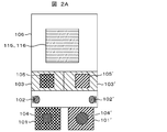
- FIG. 2A shows a top view of the inspection apparatus of the present embodiment shown in FIG.
- a sample cassette 101 containing a photomask as a first sample and a sample cassette 101 ′ containing a wafer as a second sample can be placed on the loader unit. If only one of them is inspected, one of them may be placed.
- the transport system and the sample exchange chamber each have two types of sample holders.
- the transport unit 102 takes out the sample 104 from the sample cassette 101, opens the sample exchange chamber 103 in vacuum, and opens the opening 126. Opens, the sample 104 is placed on the sample holder 105, the opening 126 shown in FIG. 1 is closed, and vacuuming is performed.
- the opening 127 is opened, the stages 115 and 116 are moved to the vicinity of the sample exchange chamber 103, and the sample holder 105 is pushed out to the stage as shown in FIG. Once fixed. After the opening 127 is closed, the stage is moved to a predetermined coordinate, and an inspection with an electron beam image is performed. When the inspection is completed, the first sample 104 is returned to the original cassette 101 in the reverse procedure described above.
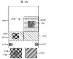
- the second sample 104 ′ is similarly moved from the cassette 101 ′ to the sample holder 105 ′ in the sample exchange chamber 103 ′ by the transport unit 102 ′.
- the stages 115 and 116 move to the vicinity of the sample exchange chamber 103 ', the opening 127' is opened, and as shown in FIG. 2C, the material holder 105 'on which the sample 104' is placed is pushed out to the stage and reaches a predetermined position.
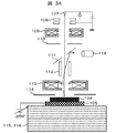
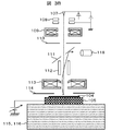
- FIG. 3 shows a schematic cross-sectional view when the sample is placed on the sample holder 105 shown in FIGS. 1 and 2 and transported to the sample chamber.
- FIG. 3A shows the case of the first sample (photomask)
- FIG. 3B shows the case of the second sample (wafer).
- the first sample holder 105 has a holding configuration that matches the size and rectangle of the mask 104, and the height of the mask surface is set to a predetermined height with respect to the electron optical system.
- the second sample holder 105 ′ has a holding configuration that matches the size and circle of the wafer 104 ′, and when the wafer is placed on the second sample holder 105 ′, the height of the wafer surface becomes an electron. It has a predetermined height with respect to the optical system.
- the same bottom surface structure of each sample holder with respect to the stage makes it possible to share and move to the sample stage in common. After fixing, it is only necessary to move according to a movement command to a predetermined coordinate.
- the holding method and thickness of the sample holder are different from the shape and thickness of each sample having different shapes so that the surface height is almost the same even for samples having different shapes.
- an electron beam image can be acquired by the same electron optical system.
- a quartz substrate that is an insulator may be used, a semiconductor substrate such as a silicon crystal may be used, or a conductive substrate such as a metal may be used.
- irradiation is performed. It is necessary to optimize the electron beam conditions (irradiation energy, electron beam current). Since the means for changing the irradiation energy is as described above, it is omitted here.
- Such optimum conditions can be applied by calling the optimum conditions registered in advance by inputting inspection conditions and recipe information from the operation unit 124. At that time, in order to control the charged state of the surface of the sample to be inspected, the condition of the voltage applied to the on-sample electrode 114 may be changed in addition to the electron beam irradiation condition.
- FIG. 4 shows an example of a coordinate system of a mask that is a first sample.
- the shape is rectangular, and the origin of the mask is the center of the mask, which is the intersection of the four corners of the mask. Since the pattern shape is inverted and transferred when transferred by the reduction exposure apparatus, the X coordinate 201 of the mask is in the mirror inverted direction, and the Y coordinate 202 is in the same direction as on the wafer. Further, since the pattern dimension is larger than the wafer according to the reduction ratio at the time of reduction exposure, the coordinates need to be converted at the same magnification. In this embodiment, a case where the reduction ratio is 1: 4 will be described.
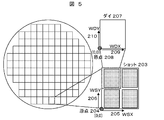
- FIG. 2 An example of a coordinate system on the wafer is shown in FIG.
- the shot 203 is divided in units to be exposed and the die 209 is a repeating unit.
- the lower left corner of the shot is the origin 204, and the coordinates are the shot X direction 205 and the shot Y direction 206.
- the lower left corner of the die is the origin 208, which is the coordinates of the die X direction 209 and the die Y direction 210.
- FIG. 6A shows a flow for converting mask coordinates into wafer coordinates.
- the offset of the origin deviation amount unique to the apparatus is adjusted (301).
- the origin 200 which is the center of the mask, is converted into the corner origin of the exposure pattern (302), and in order to match the coordinate magnification on the wafer, here the coordinate value is reduced to a quarter according to the reduction ratio ( 303).
- the direction of the coordinate system is mirror-inverted (304), and further offset adjustment is performed in accordance with the shot origin of the wafer coordinates. If the coordinates are set to die coordinates, the origin position is further adjusted in accordance with die division and die size (306).
- a flow for converting wafer coordinates into mask coordinates is shown in FIG. 6B.
- the inspection is started by inputting necessary information from the operation unit 125 (400).
- the type of sample to be inspected is selected (401).
- a cassette and a sample holder are selected, and an optimum inspection recipe registration directory is also selected.
- the electron beam irradiation conditions and the inspection recipe are loaded (402, 403).
- the inspection recipe includes selection of coordinate data to be inspected and information selection of a pattern transferred to the wafer to be inspected.
- coordinate conversion is performed by the method shown in FIG. 6 (404), and the inspection point in the coordinate system of the sample to be inspected is set. specify.
- the designated first inspection sample is loaded (405).
- the inspection of the first sample select whether to inspect the second sample subsequently.
- the inspection is executed in the same flow from the selection of the sample type shown in the flow 401 of FIG.
- the result is saved as a file in the same manner as the first sample (409).
- the inspection result of the first sample and the second inspection result are collated (412), the defect type, factor, size ratio, etc. are classified (413), and the classification result is inspected for the first and second samples.
- the result file is appended or changed, the result is output as necessary (414), and the inspection is terminated (415). Note that the sample unload timing does not have to follow the flow of FIG. If the second sample is not subsequently inspected, another past inspection result can be selected and collated with the selected result file (412). Furthermore, not only two types of test results but also three or more types of test results can be collated (412).
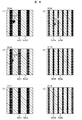
- FIG. 8 shows an example of an image acquired at the time of inspection.
- FIG. 8A is an electron beam image 500 of point 1 acquired at the time of mask inspection, and a linear pattern 501 is formed on the substrate 502.
- a defect 503 exists on the substrate 502 between the lines.
- a location (point 1) corresponding to the coordinates on the mask was inspected on the wafer.
- the result is an electron beam image 504 on the wafer shown in FIG.
- a pattern 505 formed of a material such as a photoresist exists on the film 506 formed in the lower layer.
- the defect 507 was transferred to the point 1 point. Therefore, it was determined that the defect 503 at the point 1 on the mask is a fatal defect transferred to the wafer.
- the coordinates of point 2 were similarly examined.
- the figure is an electron beam image 508 at point 2 on the mask. The pattern and the substrate are formed in the same manner. At point 2, a defect 509 exists along a linear pattern. A portion corresponding to this point 2 was inspected with a wafer.
- the figure is an electron beam image 510 on the wafer at point 2. As a result of inspecting the electron beam image 510, no defect was recognized on the wafer. Therefore, the mask-like defect at point 2 is a non-fatal defect that is not transferred to the wafer, but its presence on the mask has been confirmed, so it has been determined that it needs attention. Further, the point 3 was similarly examined. (5) The figure is an electron beam image 511 obtained by inspecting the point 3 on the mask.
- FIG. 9 shows a table A of FIG. 9 that is collated and determined by the inspection results of FIG.
- Table B in FIG. 9 is for the case where the collation inspection is performed based on the coordinates of the wafer inspection result.
- Table C in FIG. 9 is an inspection in which the dimensions of the pattern coordinates registered in advance are measured with both the mask and the wafer, and the dimension ratio is obtained.
- the inspection apparatus and the inspection method of this embodiment can load a plurality of shapes of samples into the same apparatus, and can inspect with an electron beam image based on the same coordinate data.
- the transfer source and the transfer destination sample such as a mask and a wafer
- the criticality of the defect is determined by verification. Can do.
- the defect coordinate data on the wafer it can be determined whether the cause of the defect is a process or a mask. In this manner, since the defect and quality control of the mask can be performed, the reliability of manufacturing the semiconductor device can be improved.
- the quality of the exposure process can be controlled, and the mask quality and the exposure process can be optimized. As a result, the semiconductor yield and productivity can be improved. Can contribute to the improvement.
- the template has a circuit pattern formed in the same manner as the mask, but since it is not reduced at the time of transfer, magnification conversion at the time of coordinate conversion becomes unnecessary. In addition, the pattern irregularities are reversed between the template and the wafer.
- the same effects as those of the first embodiment can be realized for a wafer on which a pattern is drawn by nanoimprinting, and it can contribute to the quality control of the template, thereby improving the productivity.
- the inspection apparatus and inspection method described so far it is possible to load a plurality of samples into the same apparatus and to inspect with an electron beam image based on the same coordinate data.
- the transfer source and the transfer destination sample such as a mask and a wafer
- the criticality of the defect is determined by verification. Can do.
- the defect coordinate data on the wafer it can be determined whether the cause of the defect is a process or a mask.
- the defect and quality control of the mask can be performed, so that the reliability of semiconductor device manufacturing can be improved.
- the quality of the exposure process can be controlled, and the mask quality and the exposure process can be optimized. As a result, the semiconductor yield and productivity can be improved. Can contribute to the improvement.
Landscapes
- Physics & Mathematics (AREA)
- General Physics & Mathematics (AREA)
- Health & Medical Sciences (AREA)
- Life Sciences & Earth Sciences (AREA)
- Chemical & Material Sciences (AREA)
- Analytical Chemistry (AREA)
- Biochemistry (AREA)
- General Health & Medical Sciences (AREA)
- Immunology (AREA)
- Pathology (AREA)
- Analysing Materials By The Use Of Radiation (AREA)
- Preparing Plates And Mask In Photomechanical Process (AREA)
- Testing Or Measuring Of Semiconductors Or The Like (AREA)
Abstract
ウエハとマスクのように同等の回路パターンが形成されているが形状が異なる試料を一つの装置で検査することができる検査装置または検査方法を提供する。 検査装置が、形状が異なる複数の試料に対応した複数の搬送ホルダを備えることにより、同一試料室で異なる試料の検査を可能とする。更に、双方の試料に対する検査結果を照合する機能を備えることにより、欠陥と欠陥が生じる原因との関係を容易に解析できるようにする。
Description
本発明は半導体装置や液晶やフォトマスクやナノインプリント等微細なパターンを有する基板製造方法及び装置に係わり、特に半導体装置とマスクのパターンに対して電子線を使用して検査する技術に関する。
特許文献1(特開2007-059176号公報)には、マスクを電子顕微鏡で観察する際に観察箇所清浄化のために紫外光を照射するようにする技術が開示されている。また、特許文献2(特開2007-220471号公報)には、予めマスク用の電子顕微鏡で取得したマスク上回路パターン画像を、ウエハ用の電子顕微鏡で電子線画像を取得する際に同時に表示する技術が開示されている。
まず、本発明の背景について、半導体装置を例として説明する。
半導体装置の製造においては、回路形成に必要なパターンをCADで設計し、この設計データをフォトマスク(レチクル)上に形成する。すなわち、透明な基板上に上記設計パターン形状が遮光膜として形成されるようにする。このフォトマスクを縮小露光装置内にロードし、感光体を塗布したウエハに対してフォトマスクを通過した光を露光,結像することで、半導体ウエハ上に回路パターンが形成される。縮小露光装置の縮小率は、一般に1/4~1/5のため、マスク上のパターンはウエハ上のパターンに対して4~5倍拡大したものになっている。
近年、半導体装置の回路微細化に伴い、ウエハ上に形成されるパターンもマスク上に形成されるパターンも小さくなってきている。縮小露光装置で露光に用いられる光の波長より小さいサイズのパターンをウエハ上に形成するために、マスクにおいて位相シフト法やOPC技術が用いられている。逆に、マスク上で微小なパターン異常や欠陥が発生した場合に、露光装置の収差や回折の影響によりウエハ上でどのような形状やサイズに転写されるか予め把握することが困難となっている。このような状況で、さらにEUVリソグラフィーでは、マスクの保護膜がなくなるために、使用時・ハンドリング時にマスク上に異物や欠陥が発生する可能性がある。また、基板が多層膜であることから、マスク上に存在する欠陥がウエハに転写されない場合や、多層膜中に埋まってマスク検査では検知が困難な欠陥がウエハ上に転写される場合があるため、マスクのみの検査、あるいはウエハのみの検査では、両者での寸法の関係,欠陥の要因,致命性の判断が困難となっている。
これまでの従来技術では、例えば半導体装置(ウエハ)については、ウエハ専用の検査装置で検査を行い、ウエハ用の検査座標データを用いてウエハ専用の電子顕微鏡で観察や寸法を測定していた。一方、フォトマスクについても同様で、マスク専用の検査装置で検査を行い、マスク用の座標データを用いてマスク専用の電子顕微鏡で観察や寸法を測定していた。上記のように、例えばEUVリソグラフィーでは、マスクの保護膜がなくなるために、使用時・ハンドリング時にマスク上に異物や欠陥が発生する可能性がある。
また、基板が多層膜であることから、マスク上に存在する欠陥がウエハに転写されない場合や、多層膜中に埋まってマスク検査では検知が困難な欠陥がウエハ上に転写される場合があるため、マスク検査とウエハに転写された結果を照合する必要がある。従来技術では、このようなマスク検査結果とウエハ検査結果の照合やレビューに膨大な時間と手間を要していた。
ナノインプリントにおいても同様に、プリントの型であるテンプレートと、転写されたパターンでの照合において、同一の装置では行えないため、別々の装置で別々に検査し、照合するのに膨大な時間を要していた。
本発明の目的は、上記課題を解決し、半導体装置や液晶やフォトマスクのようなパターンが形成された基板において、例えばウエハとマスクのように同等の回路パターンが形成されているが形状が異なる試料を一つの装置で検査することができる検査装置を提供することにある。
上記課題を解決するために、本発明では、まず、複数の形状の試料に対し、各々搬送できるロードポートを複数設けた。また、試料室の前に試料交換室を複数設け、各々の試料交換室に試料を載置するホルダを設けた。ホルダの形状,高さ,試料保持方法は、各々の試料形状に応じており、試料室内の電子光学系で観察可能な高さに試料が設置されるようになっている。また、ホルダ底面のガイドおよびステージへのアタッチメントは同一の構造であるため、単一のステージで複数のホルダに対応することができるようにした。このようにして、例えばフォトマスクと半導体ウエハを、同一の装置にロードし、電子線顕微鏡で観察あるいは計測できるようにした。
次に、マスクあるいはウエハを検査した結果ファイルあるいは測定する座標データファイルを、マスク座標とウエハ上の座標の両方に変換する座標変換手段および媒体を設けることにより、一つの検査結果でマスクとウエハの両方を同じ装置(電子顕微鏡)で観察あるいは計測できるようにした。
さらに、ウエハとマスクの両方を観察した結果を照合し、照合結果により欠陥種を分類する機能および寸法を照合し転写時の倍率比率を求める機能を設け、分類されたコードあるいは転写時の倍率比率を検査結果に追加し、検査結果データを外部に出力できるようにした。
これにより、複数の装置を用いたり人手による煩雑なデータ処理を行わなくても、同一の検査装置でマスクとウエハの両方についてSEM画像で観察あるいは寸法測定ができ、例えば欠陥がマスク起因であるかプロセス起因であるかを分類したり、例えば欠陥が致命であるか非致命であるかを分類したり、例えばパターン寸法の変動比率を求めたりすることができるようになる。
ナノインプリントのテンプレートと転写基板についても、同様である。
本発明により、短時間で効率よくフォトマスクの品質およびウエハ転写の品質を評価でき、この技術により品質を管理されたマスクを適用することで、半導体装置の品質を向上することができるため、半導体装置等の信頼性を高めるとともに不良率を低減するまでに要する期間を短縮するのに寄与することができるようになる。
(第1の実施例)
本実施例では、第一の試料としてフォトマスク、第二の試料としてウエハを検査する場合について図面を参照しながら説明する。
本実施例では、第一の試料としてフォトマスク、第二の試料としてウエハを検査する場合について図面を参照しながら説明する。
図1は、第一の実施形態に係る検査装置の全体構成を示すブロック図である。図1に示すように、本実施例の検査装置100は、試料カセット101を載置するローダと、試料104を搬送する搬送部102と、真空室である試料室106に試料104を搬送するための試料交換室103と、試料室106と、操作部124と、各部を制御する制御部123と、制御部123からの指令により電子光学系を制御するカラム制御部121と、ステージを制御するステージ制御部120と、検出器117からの信号を画像化したり記憶部122に保存したりする信号制御部119で構成されている。試料室106内には、電子光学系とステージがあり、電子源107,引き出し電極108,レンズ109,絞り110,二次電子収集用の反射板111,偏向器112,対物レンズ113,試料上電極114,Xステージ115,Yステージ116,高さセンサ117,検出器118から構成されている。
試料104は、ローダにある試料カセット101から、搬送部102により試料交換室103内の試料ホルダ105上にロードされる。試料交換室103では、試料104が載置されたら真空に引き、所定の真空度に達したら試料室106に搬送される。試料室106では、ステージ115,116が試料交換室103近くに移動し、試料ホルダ105が試料104を載せた状態でステージ115上に押し出され、固定され、試料交換室103の開口部127は閉じられる。開口部127が閉じられ、試料室106内が所定の真空度に達したら、ステージ115,116が所定の座標に移動し電子線画像を取得する。電子線は、電子源107から発せられ、引き出し電極108で加速され、レンズ109で絞られて絞り110を通過し、対物レンズ113で絞られ試料104上で焦点を結ぶ。この電子線は偏向器112で走査され、これと同期して検出器118で信号を逐次検出し、信号値を濃淡値に変換して電子線画像とする。検出器118に二次電子あるいは反射電子を収集するために、反射板111が用いられている。試料台105には電圧が印加できるようになっており、試料に照射される電子線のエネルギーを調整できる。電子源107と引き出し電極108にも電圧が印加されているので、これらの電圧調整の組み合わせにより試料へ照射されるエネルギーが制御される。検出器118で検出された信号は、信号制御部119にて変換・画像化され、保存する場合には記憶部122にデータを格納する。これらの一連の動作は、操作部124から命令が入力され、それに基づき制御部123が各部に制御命令を与えることで実行される。さらに、制御部123は外部とネットワーク通信等でつながっており、外部データベース125とアクセスできる。例えば、他の装置で検査した座標データを授受したり、本実施例の検査装置の検査結果データや保存した画像データを出力することができる。
図2Aには、図1に示した本実施例の検査装置の上面図を示す。ローダ部には、第一の試料であるフォトマスクの入った試料カセット101と、第二の試料であるウエハが入った試料カセット101′が載置できる。片方のみを検査する場合にはいずれか一方を載置すれば良い。搬送系,試料交換室は、試料ホルダは各々2式あり、第一の試料の場合には、試料カセット101から搬送部102が試料104を取り出し、試料交換室103を真空開放し、開口部126が開き、試料104を試料ホルダ105に載せ、図1に示す開口部126を閉じ真空引きを行う。所定の真空度に達したら、開口部127が開き、ステージ115,116が試料交換室103近くに移動し、更に図2Bに示されるように試料ホルダ105がステージまで押し出され、所定の位置に達したら固定される。開口部127が閉じた後、ステージが所定の座標に移動し、電子線画像による検査を行う。検査が終了したら、上記の逆の手順で第一の試料104はもとのカセット101に戻される。
第二の試料を検査する場合には、同様にカセット101′から搬送部102′により第二の試料104′を試料交換室103′内の試料ホルダ105′上に移動させる。ステージ115,116が試料交換室103′近くに移動し、開口部127′が開き、図2Cに示されるように試料104′が載った資料ホルダ105′がステージまで押し出され、所定の位置に達したら固定される。
図3に、図1および図2で示した試料ホルダ105に試料を載置させ試料室に搬送させた場合の断面模式図を示す。図3Aが第一の試料(フォトマスク)の場合、図3Bが第二の試料(ウエハ)の場合である。第一の試料ホルダ105は、マスク104のサイズと矩形にあわせた保持形態となっており、マスク表面の高さが電子光学系に対して所定の高さになるようになっている。第二の試料ホルダ105′は、ウエハ104′のサイズと円形にあわせた保持形態となっており、第二の試料ホルダ105′上にウエハが載置された際にウエハ表面の高さが電子光学系に対して所定の高さになるようになっている。このように、複数の形状の被検査試料を同一の検査装置100で検査する場合に、ステージに対して各試料ホルダの下面構造を同じくすることで、試料台への移動および固定方法を共通にでき、固定した後には、所定の座標への移動命令に従って移動すればよいことになる。
一方、電子光学系に対しては、形状の異なる試料であっても表面高さがほぼ同じになるように、形状の異なる各試料の形状や厚みに対して試料ホルダの保持方法および厚さで調整することで、同じ電子光学系により電子線画像を取得することができるようになる。試料によっては、絶縁物である石英基板を用いる場合や、シリコン結晶のような半導体基板を用いる場合や、金属のような導電性基板を用いる場合があり、同じ電子光学系であっても照射する電子線の条件(照射エネルギー,電子ビーム電流)を各々最適化する必要がある。照射エネルギーを変える手段については、前記のとおりなのでここでは省略する。このような最適条件は、操作部124より検査条件やレシピ情報を入力することで予め登録しておいた最適条件を呼び出し適用することができる。その際に、被検査試料表面の帯電状態を制御するため、上記電子線の照射条件に加えて試料上電極114に印加する電圧の条件も変える場合がある。
次に、本実施例の検査装置100を用いて検査する方法について説明する。まず、第一の試料であるマスクの座標系の一例を図4に示す。形状は矩形で、マスクの四隅の交点であるマスク中心が原点200となっている。縮小露光装置で転写される時に、パターン形状が反転して転写されるため、マスクのX座標201はミラー反転した向きとなっており、Y座標202はウエハ上と同じ向きである。また、縮小露光時の縮小率に応じて、パターン寸法がウエハより大きいため、座標も同じ倍率で換算する必要がある。本実施例では、縮小率が1:4の場合について説明する。
次に、ウエハ上での座標系の一例を図5に示す。露光される単位でのショット203,繰り返しの単位であるダイ209毎に分割されている。ショット203の座標系は、ショットの左下のコーナーが原点204であり、ショットX方向205とショットY方向206の座標となっている。ダイ207単位の場合にも同様に、ダイの左下のコーナーが原点208であり、ダイX方向209とダイY方向210の座標となっている。
このように、形状や倍率の異なる試料でマスク上とウエハ上で等価のパターン箇所を検査する場合、図6に示す座標換算が必要になる。図6のA図は、マスク座標をウエハ座標に変換するフローを示している。マスク座標値MX1,MY1(300)に対し、装置固有の原点ずれ量のオフセットを調整する(301)。次に、マスク中心となっている原点200を露光パターンのコーナー原点に変換し(302)、ウエハでの座標倍率にあわせるため、ここでは座標値を縮小率にあわせて4分の1にする(303)。そして、座標系の向きをミラー反転し(304)、ウエハ座標のショット原点にあわせてさらにオフセット調整する。もしダイ座標にする場合には、さらにダイ分割とダイサイズにあわせて原点位置を調整する(306)。逆に、ウエハの座標をマスク座標に変換するフローを図6のB図に示す。
図1の検査装置を用いて、実際に被検査試料を検査する方法について、図7を参照しながら説明する。操作部125より必要な情報を入力して検査を開始する(400)。最初に、被検査試料のタイプを選択する(401)。これにより、カセットや試料ホルダが選択され、最適な検査レシピの登録ディレクトリも選択される。操作画面より、電子線照射条件および検査レシピをロードする(402,403)。検査レシピには、検査すべき座標データの選択および被検査ウエハに転写されているパターンの情報選択が含まれる。次に、レシピでロードした座標データが、被検査試料と同一の座標系でない場合には、図6に示した方法で座標変換を行い(404)、被検査試料の座標系での検査ポイントを指定する。そして、指定した第一の被検査試料をロードする(405)。
次に、被検査試料上に形成されたパターンの光学顕微鏡画像や電子線画像を用いて、試料の位置や回転量を求め補正するためのアライメントを実行する(406)。さらに、既知のパターンに移動し、座標のオフセット量を補正した後(407)、上記レシピでロードし座標変換された座標に基づきステージを移動し電子線画像を取得し、必要に応じて画像を保存したり寸法を計測する(408)。このようにして、所望の箇所について検査を実行し、結果をファイルとして保存し、必要に応じて結果を出力する(409)。
第一の試料の検査が終了したら、次に続けて第二の試料を検査するかどうかを選択する。第二の試料を選択した場合には、図7のフロー401に示す、試料タイプの選択から同様のフローで検査を実行する。第二の試料の検査が終了したら、第一の試料と同様に結果をファイルとして保存する(409)。その後、第一の試料の検査結果と第二の検査結果を照合し(412)、欠陥の種類や要因、寸法比率等を分類し(413)、分類結果を第一および第二の試料の検査結果ファイルに追記あるいは変更し、必要に応じて結果を出力し(414)、検査を終了する(415)。なお、試料のアンロードのタイミングは、図7のフロー通りでなくても良い。また、続けて第二の試料を検査しない場合には、過去の別の検査結果を選択し、該選択した結果ファイルと照合することができる(412)。さらに、2種の検査結果だけでなく、3種以上の検査結果を照合することもできる(412)。
図8に、検査時に取得した画像の例を示す。図8の(1)図は、マスク検査時に取得されたポイント1の電子線画像500で、基板502上に線状のパターン501が形成されている。線と線の間の基板502上に欠陥503が存在している。このマスク上の座標に相当する箇所(ポイント1)を、次にウエハ上で検査した。その結果が(2)図に示すウエハ上の電子線画像504である。下層に形成された膜506上にフォトレジスト等の材料で形成されたパターン505が存在している。電子線画像を検査した結果、ポイント1の箇所に欠陥507が転写されていることが判明した。よって、マスク上のポイント1の欠陥503は、ウエハに転写される致命性の欠陥であることが判定された。ポイント2の座標について、同様に検査した。(3)図はマスク上ポイント2の電子線画像508である。パターンと基板が同様に形成されている。ポイント2では、線状のパターンに沿って欠陥509が存在している。このポイント2に相当する箇所をウエハで検査した。(4)図はポイント2のウエハ上での電子線画像510である。この電子線画像510を検査した結果ウエハ上では、欠陥は認識できなかった。従って、ポイント2のマスク状の欠陥は、ウエハに転写されない非致命の欠陥であるが、マスク上に存在が確認されたので要注意と判定された。さらに、ポイント3の箇所を同様に検査した。(5)図はポイント3の箇所をマスク上で検査した電子線画像511である。検査の結果、欠陥は認識できなかった。ウエハ上のポイント3についても、(6)図に示す電子線画像512の検査の結果、欠陥は認識されなかった。従って、ポイント3の座標は、事前の検査装置での誤検出と判定された。
図8の検査結果で照合され、判定された結果を図9の表Aに示す。このようにして、マスクとウエハの両方を同じ検査結果の座標データを用いて照合検査することで、欠陥の致命性および欠陥発生要因がマスクであるかプロセスであるかを大まかに分類できる。図9の表Bは、ウエハ検査結果の座標をもとに照合検査を行った場合についてのものである。さらに図9の表Cについては、予め登録したパターンの座標について、マスクとウエハの両方で寸法を計測し、その寸法比率を求めた検査となっている。
本実施例の検査装置および検査方法により、複数の形状の試料を同じ装置にロードすることができ、同じ座標データに基づいて電子線画像により検査することができるようになった。また、例えばマスクとウエハのように、転写元と転写先の試料を照合して検査することができるため、例えばマスク上の欠陥座標データを用いると、照合により該欠陥の致命性を判定することができる。一方、ウエハ上での欠陥座標データを用いると、欠陥の要因がプロセス起因かマスク起因かを判定することができるようになる。このようにして、マスクの欠陥および品質管理を行うことができるようになるので、半導体装置製造の信頼性を向上することができるようになる。また、露光プロセスマージンとの関連性や、寸法管理もできるため、露光プロセスの品質管理もできるようになり、マスク品質および露光プロセスの最適化を図ることができ、結果として半導体の歩留まりや生産性を高めることに寄与できる。
(第2の実施例)
本実施例では、第1の実施例で説明した第一の試料(フォトマスク)がナノインプリントで用いられるテンプレートであり、第二の試料がウエハの場合のパターン検査装置の構成例を示す。装置の全体構成および機能・動作は第1の実施例と同様であり、説明は省略する。
本実施例では、第1の実施例で説明した第一の試料(フォトマスク)がナノインプリントで用いられるテンプレートであり、第二の試料がウエハの場合のパターン検査装置の構成例を示す。装置の全体構成および機能・動作は第1の実施例と同様であり、説明は省略する。
テンプレートは、マスクと同様に回路パターンを形成されているが、転写時に縮小されないために座標変換時の倍率変換が不要となる。また、パターンの凹凸が、テンプレートとウエハで反転するという特徴がある。
本実施例により、ナノインプリントによるパターン描画を行うウェハに対しても第1の実施例と同様な作用効果が実現でき、更にテンプレートの品質管理に寄与でき、生産性を高めることができるようになる。
以上、本発明の代表的な装置構成および検査方法について具体的な各部の作用,検査フロー,操作手順,照合方法等の実施例について説明してきたが、特許請求の範囲あるいは各実施例に掲げた複数の特徴を組み合わせた検査装置および検査方法についても、本発明の範囲を逸脱しない範囲で実施可能であることは言うまでもない。
また、これまでに述べてきた検査装置および検査方法により、複数の形状の試料を同じ装置にロードすることができ、同じ座標データに基づいて電子線画像により検査することができるようになった。また、例えばマスクとウエハのように、転写元と転写先の試料を照合して検査することができるため、例えばマスク上の欠陥座標データを用いると、照合により該欠陥の致命性を判定することができる。一方、ウエハ上での欠陥座標データを用いると、欠陥の要因がプロセス起因かマスク起因かを判定することができるようになる。
このようにして、マスクの欠陥および品質管理を行うことができるようになるので、半導体装置製造の信頼性を向上することができるようになる。また、露光プロセスマージンとの関連性や、寸法管理もできるため、露光プロセスの品質管理もできるようになり、マスク品質および露光プロセスの最適化を図ることができ、結果として半導体の歩留まりや生産性を高めることに寄与できる。
100 検査装置
101 試料カセット
102 搬送部
103 試料交換室
104 被検査試料
105 試料ホルダ
106 試料室
107 電子源
108 引き出し電極
109 レンズ
110 絞り
111 反射板
112 偏向器
113 対物レンズ
114 試料上電極
115 Xステージ
116 Yステージ
117 高さセンサ
118 検出器
119 信号制御部
120 ステージ制御部
121 光学系制御部
122 記憶部
123 制御部
124 操作部
125 外部データベース,媒体
126 搬送部側開口部
127 試料室側開口部
200 マスク原点
201 マスクX座標
202 マスクY座標
203 ショット
204 ショット原点
205 ショットX座標
206 ショットY座標
207 ダイ
208 ダイ原点
209 ダイX座標
210 ダイY座標
300 マスク座標(フロー)
301,311 オフセット調整(フロー)
302 センター原点→コーナー原点(フロー)
303 倍率変換(4分の1)(フロー)
304,308 ミラー変換(フロー)
305 ショット座標系→ダイ座標系変換(フロー)
306 ダイ座標系(フロー)
307 ダイ座標系→ショット座標系(フロー)
309 倍率変換(4倍)(フロー)
310 コーナー原点→センター原点(フロー)
400~415 検査フローの各動作
500 ポイント1のマスク上の電子線画像
501 マスク上のパターン
502 マスク上の基板
503 マスク上で見つかった欠陥
504 ポイント2のウエハ上の電子線画像
505 ウエハ上のパターン
506 ウエハ上下層の膜
507 ウエハ上で見つかった欠陥
101 試料カセット
102 搬送部
103 試料交換室
104 被検査試料
105 試料ホルダ
106 試料室
107 電子源
108 引き出し電極
109 レンズ
110 絞り
111 反射板
112 偏向器
113 対物レンズ
114 試料上電極
115 Xステージ
116 Yステージ
117 高さセンサ
118 検出器
119 信号制御部
120 ステージ制御部
121 光学系制御部
122 記憶部
123 制御部
124 操作部
125 外部データベース,媒体
126 搬送部側開口部
127 試料室側開口部
200 マスク原点
201 マスクX座標
202 マスクY座標
203 ショット
204 ショット原点
205 ショットX座標
206 ショットY座標
207 ダイ
208 ダイ原点
209 ダイX座標
210 ダイY座標
300 マスク座標(フロー)
301,311 オフセット調整(フロー)
302 センター原点→コーナー原点(フロー)
303 倍率変換(4分の1)(フロー)
304,308 ミラー変換(フロー)
305 ショット座標系→ダイ座標系変換(フロー)
306 ダイ座標系(フロー)
307 ダイ座標系→ショット座標系(フロー)
309 倍率変換(4倍)(フロー)
310 コーナー原点→センター原点(フロー)
400~415 検査フローの各動作
500 ポイント1のマスク上の電子線画像
501 マスク上のパターン
502 マスク上の基板
503 マスク上で見つかった欠陥
504 ポイント2のウエハ上の電子線画像
505 ウエハ上のパターン
506 ウエハ上下層の膜
507 ウエハ上で見つかった欠陥
Claims (14)
- パターンが形成された基板表面に電子線を照射する手段と、該基板から発生する信号を検出する手段と、検出手段により検出された信号を画像化する手段から成るパターン検査装置であって、
複数の試料ロードポートと複数の試料交換室を有し、該試料交換室に各々形状の異なる試料を載置するための複数のホルダを有し、該試料ホルダにより形状の異なる試料を同一ステージに載置する手段を備えていることを特徴とするパターン検査装置。 - 請求項1に記載のパターン検査装置において、
試料の一つは、半導体装置のマスク(第一の試料)であり、もう一つは半導体ウエハ(第二の試料)であることを特徴とするパターン検査装置。 - 請求項1に記載のパターン検査装置において、
試料の一つはテンプレートであり、もう一つ該テンプレートで転写されたパターンが形成された基板あるいはフィルムであることを特徴とするパターン検査装置。 - 請求項1から3のいずれか1項に記載のパターン検査装置において、
他の装置で被検査試料を検査した結果の座標データをもとに、該座標データを複数の試料形状にあわせて各々変換する手段と、
変換した結果に基づきアライメントを行う手段と、
アライメント後に該座標に移動し画像を取得する手段を備えていることを特徴とするパターン検査装置。 - 請求項1から3のいずれか1項に記載のパターン検査装置において、
検査手段として、他の装置で検出された座標に基づき該試料の当該箇所を観察する手段と、
予め登録された座標に基づき当該箇所を観察する手段または予め登録された座標に基づき当該パターンの寸法を計測する手段のいずれか一つの手段を備えていることを特徴とするパターン検査装置。 - 請求項2および5のいずれか1項に記載のパターン検査装置において、
前記複数の試料ホルダのうち一つが第一の試料用試料ホルダであり、一つが第二の試料用試料ホルダであって、
前記第一の試料の当該箇所寸法を計測した結果と第二の試料の当該箇所寸法を計測した結果を比較する手段と、比較した結果より転写倍率を求める手段と、各箇所の転写倍率計測結果を出力する手段とを有することを特徴とするパターン検査装置。 - 請求項2または3のいずれか1項に記載のパターン検査装置において、
前記第一の試料を検査した結果と第二の試料を検査した結果を照合する手段と、
当該照合した結果に基づき欠陥を分類するデータ処理手段と、
当該分類した結果を出力する手段を有することを特徴とするパターン検査装置。 - 第一の試料を試料室に搬送する工程と、被検査試料を検査する座標データをロードする工程と、該座標データを試料形状タイプに応じて変換する工程と、変換座標に応じてアライメントする工程と、変換された座標データに基づき第一の試料を移動する工程と、電子線画像を取得する工程と、第二の試料を試料室に搬送する工程と、該座標データを第二の試料タイプに応じて変換する工程と、変換座標に応じてアライメントする工程と、変換された座標データに基づき第二の試料を移動する工程と、電子線画像を取得する工程とを含むパターン検査方法であって、
第一の試料を検査した結果と第二の試料を検査した結果を照合する工程と、
照合した結果に基づき欠陥を分類する工程と、
分類された結果を追加された検査結果データを出力する工程を含むことを特徴とするパターン検査方法。 - 請求項8に記載の検査方法であって、
第一の試料における所定の検査対象座標を第二の試料形状にあわせて変換する工程を含むことを特徴とするパターン検査方法。 - 請求項8に記載の検査方法であって、
前記照合した結果に基づき欠陥を分類する工程および前記分類された結果を検査結果データに追加する工程と該検査結果データを出力する工程において、最初の検査対象座標データを求めた装置あるいは媒体に対し変更を施す工程を含むことを特徴とするパターン検査方法。 - 請求項1に記載のパターン検査装置において、
第一の試料ホルダと第二の試料ホルダの下面は同じ構造であることを特徴とするパターン検査装置。 - 請求項1に記載のパターン検査装置において、
第一の試料が第一の試料ホルダに載置され試料室内の試料台に載置された際の試料表面高さと、第二の試料が第二の試料ホルダに載置され試料室内の試料台に載置された際の試料表面高さとが、ほぼ同等になる構造であることを特徴とするパターン検査装置。 - 請求項1および2の検査装置で検査を施され品質を管理されたマスクおよび該マスクで転写された半導体装置。
- 請求項1および3の検査装置で検査を施され品質を管理されたテンプレートおよび該テンプレートで転写された基板あるいはフィルム。
Applications Claiming Priority (2)
| Application Number | Priority Date | Filing Date | Title |
|---|---|---|---|
| JP2011-110002 | 2011-05-17 | ||
| JP2011110002A JP2012243831A (ja) | 2011-05-17 | 2011-05-17 | パターン検査装置および検査方法 |
Publications (1)
| Publication Number | Publication Date |
|---|---|
| WO2012157181A1 true WO2012157181A1 (ja) | 2012-11-22 |
Family
ID=47176536
Family Applications (1)
| Application Number | Title | Priority Date | Filing Date |
|---|---|---|---|
| PCT/JP2012/002410 Ceased WO2012157181A1 (ja) | 2011-05-17 | 2012-04-06 | パターン検査装置および検査方法 |
Country Status (2)
| Country | Link |
|---|---|
| JP (1) | JP2012243831A (ja) |
| WO (1) | WO2012157181A1 (ja) |
Families Citing this family (4)
| Publication number | Priority date | Publication date | Assignee | Title |
|---|---|---|---|---|
| JP6379937B2 (ja) * | 2014-09-30 | 2018-08-29 | 大日本印刷株式会社 | ステージ制御方法、修正テンプレートの製造方法、およびテンプレート観察修正装置 |
| WO2018016062A1 (ja) | 2016-07-22 | 2018-01-25 | 株式会社 日立ハイテクノロジーズ | パターン評価装置 |
| JP7220126B2 (ja) * | 2019-06-14 | 2023-02-09 | 株式会社ニューフレアテクノロジー | 検査装置 |
| CN121721896A (zh) * | 2020-04-30 | 2026-03-24 | 美商福昌公司 | 用于制造光掩模的系统、方法和程序产品 |
Citations (2)
| Publication number | Priority date | Publication date | Assignee | Title |
|---|---|---|---|---|
| WO2002001596A1 (fr) * | 2000-06-27 | 2002-01-03 | Ebara Corporation | Appareil d'inspection d'un faisceau de particules charge et procede de production d'un dispositif utilisant cet appareil |
| JP2009036703A (ja) * | 2007-08-03 | 2009-02-19 | Toppan Printing Co Ltd | パターン計測装置及びパターン計測方法 |
-
2011
- 2011-05-17 JP JP2011110002A patent/JP2012243831A/ja not_active Withdrawn
-
2012
- 2012-04-06 WO PCT/JP2012/002410 patent/WO2012157181A1/ja not_active Ceased
Patent Citations (2)
| Publication number | Priority date | Publication date | Assignee | Title |
|---|---|---|---|---|
| WO2002001596A1 (fr) * | 2000-06-27 | 2002-01-03 | Ebara Corporation | Appareil d'inspection d'un faisceau de particules charge et procede de production d'un dispositif utilisant cet appareil |
| JP2009036703A (ja) * | 2007-08-03 | 2009-02-19 | Toppan Printing Co Ltd | パターン計測装置及びパターン計測方法 |
Also Published As
| Publication number | Publication date |
|---|---|
| JP2012243831A (ja) | 2012-12-10 |
Similar Documents
| Publication | Publication Date | Title |
|---|---|---|
| JP7035069B2 (ja) | 2つのフォトマスクを比較することによるフォトマスクの検査 | |
| KR102244485B1 (ko) | 리소그래피 제조 프로세스에 관련된 진단 정보를 획득하기 위한 방법 및 장치, 진단 장치를 포함하는 리소그래피 처리 시스템 | |
| US9552963B2 (en) | Charged particle beam writing apparatus and method therefor | |
| US9406573B2 (en) | Exposure mask fabrication method, exposure mask fabrication system, and semiconductor device fabrication method | |
| CN107924852A (zh) | 用于基于模型的临界尺寸测量的技术及系统 | |
| WO2013173468A2 (en) | Method and device for using substrate geometry to determine substrate analysis sampling | |
| JP2019502952A (ja) | インスペクションのための方法及び装置 | |
| WO2007125853A1 (ja) | 測定検査方法、測定検査装置、露光方法、デバイス製造方法及びデバイス製造装置 | |
| KR20170051506A (ko) | 극자외선 파장 범위용 마스크를 제조하는 방법, 마스크 및 장치 | |
| JP2012059984A (ja) | マスク検査装置及び露光用マスク製造装置 | |
| EP4327082B1 (en) | FAULT DETECTION FOR MULTI-CHIP MASKS | |
| CN115427893A (zh) | 从图像中去除伪影 | |
| TWI887539B (zh) | 缺陷檢查裝置、缺陷檢查方法及空白光罩之製造方法 | |
| WO2012157181A1 (ja) | パターン検査装置および検査方法 | |
| KR20170057867A (ko) | 검사 방법 및 검사 장치 | |
| US20250314958A1 (en) | Contaminant identification metrology system, lithographic apparatus, and methods thereof | |
| US10504219B2 (en) | Inspection apparatus and inspection method | |
| TWI723385B (zh) | 檢測工具、檢測方法及電腦程式產品 | |
| CN111566776B (zh) | 检查工具和确定检查工具的畸变的方法 | |
| JP2021516865A (ja) | 検査システム、リソグラフィ装置、及び検査方法 | |
| US8331647B2 (en) | Method of determining defect size of pattern used to evaluate defect detection sensitivity and method of creating sensitivity table | |
| JP7737505B2 (ja) | マイクロリソグラフィ微細構造試料の像を分析するための方法およびデバイス | |
| US12253472B2 (en) | System and method for detecting a defect in a specimen | |
| KR20260041861A (ko) | 공간적으로 변화하는 투과율을 갖는 동공 필터 |
Legal Events
| Date | Code | Title | Description |
|---|---|---|---|
| 121 | Ep: the epo has been informed by wipo that ep was designated in this application |
Ref document number: 12784893 Country of ref document: EP Kind code of ref document: A1 |
|
| NENP | Non-entry into the national phase |
Ref country code: DE |
|
| 122 | Ep: pct application non-entry in european phase |
Ref document number: 12784893 Country of ref document: EP Kind code of ref document: A1 |