WO2012157242A1 - 非絶縁降圧スイッチングレギュレータおよびその制御回路、電子機器、acアダプタ - Google Patents
非絶縁降圧スイッチングレギュレータおよびその制御回路、電子機器、acアダプタ Download PDFInfo
- Publication number
- WO2012157242A1 WO2012157242A1 PCT/JP2012/003125 JP2012003125W WO2012157242A1 WO 2012157242 A1 WO2012157242 A1 WO 2012157242A1 JP 2012003125 W JP2012003125 W JP 2012003125W WO 2012157242 A1 WO2012157242 A1 WO 2012157242A1
- Authority
- WO
- WIPO (PCT)
- Prior art keywords
- signal
- terminal
- input
- voltage
- output
- Prior art date
- Legal status (The legal status is an assumption and is not a legal conclusion. Google has not performed a legal analysis and makes no representation as to the accuracy of the status listed.)
- Ceased
Links
Images



Classifications
-
- H—ELECTRICITY
- H02—GENERATION; CONVERSION OR DISTRIBUTION OF ELECTRIC POWER
- H02M—APPARATUS FOR CONVERSION BETWEEN AC AND AC, BETWEEN AC AND DC, OR BETWEEN DC AND DC, AND FOR USE WITH MAINS OR SIMILAR POWER SUPPLY SYSTEMS; CONVERSION OF DC OR AC INPUT POWER INTO SURGE OUTPUT POWER; CONTROL OR REGULATION THEREOF
- H02M7/00—Conversion of AC power input into DC power output; Conversion of DC power input into AC power output
- H02M7/02—Conversion of AC power input into DC power output without possibility of reversal
- H02M7/04—Conversion of AC power input into DC power output without possibility of reversal by static converters
- H02M7/06—Conversion of AC power input into DC power output without possibility of reversal by static converters using discharge tubes without control electrode or semiconductor devices without control electrode
-
- H—ELECTRICITY
- H02—GENERATION; CONVERSION OR DISTRIBUTION OF ELECTRIC POWER
- H02M—APPARATUS FOR CONVERSION BETWEEN AC AND AC, BETWEEN AC AND DC, OR BETWEEN DC AND DC, AND FOR USE WITH MAINS OR SIMILAR POWER SUPPLY SYSTEMS; CONVERSION OF DC OR AC INPUT POWER INTO SURGE OUTPUT POWER; CONTROL OR REGULATION THEREOF
- H02M3/00—Conversion of DC power input into DC power output
- H02M3/02—Conversion of DC power input into DC power output without intermediate conversion into AC
- H02M3/04—Conversion of DC power input into DC power output without intermediate conversion into AC by static converters
- H02M3/10—Conversion of DC power input into DC power output without intermediate conversion into AC by static converters using discharge tubes with control electrode or semiconductor devices with control electrode
- H02M3/145—Conversion of DC power input into DC power output without intermediate conversion into AC by static converters using discharge tubes with control electrode or semiconductor devices with control electrode using devices of a triode or transistor type requiring continuous application of a control signal
- H02M3/155—Conversion of DC power input into DC power output without intermediate conversion into AC by static converters using discharge tubes with control electrode or semiconductor devices with control electrode using devices of a triode or transistor type requiring continuous application of a control signal using semiconductor devices only
- H02M3/156—Conversion of DC power input into DC power output without intermediate conversion into AC by static converters using discharge tubes with control electrode or semiconductor devices with control electrode using devices of a triode or transistor type requiring continuous application of a control signal using semiconductor devices only with automatic control of output voltage or current, e.g. switching regulators
-
- H—ELECTRICITY
- H02—GENERATION; CONVERSION OR DISTRIBUTION OF ELECTRIC POWER
- H02M—APPARATUS FOR CONVERSION BETWEEN AC AND AC, BETWEEN AC AND DC, OR BETWEEN DC AND DC, AND FOR USE WITH MAINS OR SIMILAR POWER SUPPLY SYSTEMS; CONVERSION OF DC OR AC INPUT POWER INTO SURGE OUTPUT POWER; CONTROL OR REGULATION THEREOF
- H02M1/00—Details of apparatus for conversion
- H02M1/0003—Details of control, feedback or regulation circuits
-
- H—ELECTRICITY
- H02—GENERATION; CONVERSION OR DISTRIBUTION OF ELECTRIC POWER
- H02M—APPARATUS FOR CONVERSION BETWEEN AC AND AC, BETWEEN AC AND DC, OR BETWEEN DC AND DC, AND FOR USE WITH MAINS OR SIMILAR POWER SUPPLY SYSTEMS; CONVERSION OF DC OR AC INPUT POWER INTO SURGE OUTPUT POWER; CONTROL OR REGULATION THEREOF
- H02M1/00—Details of apparatus for conversion
- H02M1/0003—Details of control, feedback or regulation circuits
- H02M1/0009—Devices or circuits for detecting current in a converter
Definitions
- the present invention relates to a non-insulated step-down switching regulator (DC / DC converter).
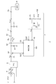
- FIG. 1 is a circuit diagram showing a configuration of a non-insulated step-down switching regulator investigated by the present inventors.
- the switching regulator 2r steps down the DC input voltage VIN of the input terminal P1 and outputs it to the output terminal P2.
- the switching regulator 2r includes a switching transistor M1, which is an N-channel MOSFET, a rectifier diode D1, an inductor L1, an output capacitor C1, a current detection resistor Rs, a control circuit 100r, and a feedback circuit 102.
- a switching transistor M1 which is an N-channel MOSFET, a rectifier diode D1, an inductor L1, an output capacitor C1, a current detection resistor Rs, a control circuit 100r, and a feedback circuit 102.
- One end of the current detection resistor Rs is connected to the switching transistor M1, and the other end is connected to the cathode of the rectifier diode D1.
- One end of the inductor L1 is connected to the cathode of the rectifier diode D1, and the other end is connected to the output capacitor C1.
- the control circuit 100r is a current mode or voltage mode pulse width modulation control circuit, and includes a current detection terminal CS, a switching terminal OUT, a feedback terminal FB, and a ground terminal GND.
- the control circuit 100r switching terminal OUT is connected to the gate of the switching transistor M1, its ground terminal GND is connected to the cathode of the rectifier diode D1, and its current detection terminal CS is connected to one end of the current detection resistor Rs.
- the current detection resistor Rs the ON period of the switching transistor M1, the coil current I L of the inductor L1 flows, a voltage drop proportional to the coil current I L (the detection voltage Vs) is generated.
- the detection voltage Vs is fed back to the current detection terminal CS.
- the feedback circuit 102 generates a feedback voltage V FB corresponding to the output voltage VOUT of the switching regulator 2r, and inputs it to the feedback terminal FB of the control circuit 100r.
- the feedback circuit 102 includes, for example, a photocoupler, and functions as an error amplifier that generates a feedback voltage V FB corresponding to an error between the output voltage VOUT and a target value.
- Control circuit 100r while maintaining the coil current I L at a constant level according to the detected voltage Vs, so that the output voltage V OUT corresponding to the feedback voltage V FB coincides with the target value, pulse signal having a duty ratio adjusted S PWM is generated and output from the switching terminal OUT.
- control circuit 100r turns on the switching transistor M1 every predetermined cycle.
- the switching transistor M1 is turned on, the coil current I L of the inductor L1 increases with time, also the detection voltage Vs increases accordingly.
- Control circuit 100r when the detection voltage Vs reaches the feedback voltage V FB, in other words, the coil current I L reaches a current value is adjusted according to the output voltage V OUT, it turns off the switching transistor M1. By repeating the above operation, the control circuit 100r switches the switching transistor M1.
- the switching transistor M1 is not switched off every cycle, at least during the mask time T MSK , and is turned on. That is, the mask time T MSK is the minimum on-time of the switching transistor M1.
- FIG. 2 is a waveform diagram when the output is grounded in the switching regulator 2r of FIG.
- the vertical and horizontal axes of the waveform diagrams and time charts in this specification are enlarged or reduced as appropriate for easy understanding, and each waveform shown is also simplified for easy understanding. Yes.
- the same problem may occur not only in the ground fault state of the output terminal but also in the state where the output voltage VOUT is low immediately after the switching regulator 2r is started.
- the present invention has been made in view of the above problems, and one of the exemplary purposes of an embodiment thereof is to provide a switching regulator with improved reliability in a low output voltage state.
- the switching regulator receives an input voltage at an input terminal and outputs an output voltage stepped down from the output terminal.
- the switching regulator includes a switching transistor, a detection resistor and an inductor provided in series between an input terminal and an output terminal in order, a rectifier diode provided between a connection point of the switching transistor and the detection resistor, and a ground terminal, and an output terminal And an output capacitor provided between the ground terminal and the ground terminal.
- the control circuit includes a switching terminal to be connected to the control terminal of the switching transistor, a current detection terminal to be connected to a connection point between the switching transistor and the detection resistor, and a ground terminal to be connected to a connection point between the detection resistor and the inductor.
- the coil current flows not only in the on period of the switching transistor but also in the off period in the current detection resistor, the coil current can be monitored over both the on period and the off period.
- the output voltage decreases due to a ground fault at the output terminal of the switching regulator, the coil current flowing through the inductor gradually increases, and an overcurrent state is detected by the current limiting comparator.
- the current limiting signal generated by the current limiting comparator is continuously asserted regardless of the on period or the off period. Then, by masking the set signal with this current limiting signal, the switching transistor does not transition to the first level, so that the switching transistor can be kept off, and the coil current can be prevented from continuing to rise. As a result, the reliability of the circuit can be improved.
- This switching regulator includes a switching transistor, a detection resistor and an inductor provided in series between an input terminal and an output terminal in order, a rectifier diode provided between a connection point of the switching transistor and the detection resistor, and a ground terminal, and an output.
- An output capacitor provided between the terminal and the ground terminal, and the above-described control circuit for driving the switching transistor.
- Yet another embodiment of the present invention is an electronic device.
- This electronic apparatus includes the above-described switching regulator.
- Yet another embodiment of the present invention is an AC adapter.
- This AC adapter includes the above-described switching regulator.
- FIG. 4 is a circuit diagram illustrating a configuration of a control circuit in FIG. 3.
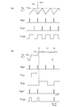
- FIGS. 5A and 5B are waveform diagrams showing the operation of the switching regulator of FIG. It is a figure which shows an AC adapter provided with a switching regulator.
- 7A and 7B are diagrams illustrating an electronic device including a switching regulator.
- the state in which the member A is connected to the member B means that the member A and the member B are physically directly connected, or the member A and the member B are electrically connected to each other. Including the case of being indirectly connected through other members that do not substantially affect the state of connection, or do not impair the functions and effects achieved by the combination thereof.
- the state in which the member C is provided between the member A and the member B refers to the case where the member A and the member C or the member B and the member C are directly connected, as well as their electric It includes cases where the connection is indirectly made through other members that do not substantially affect the general connection state, or that do not impair the functions and effects achieved by their combination.
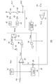
- FIG. 3 is a circuit diagram illustrating a configuration of the electronic apparatus 1 according to the embodiment.
- the electronic device 1 is, for example, a home appliance such as a television, a refrigerator, or an air conditioner, or a computer.
- the electronic device 1 includes a switching regulator 2, a rectifier circuit 4, a PFC (power factor correction) circuit 6, and a load 8.
- the rectifier circuit 4 is a diode rectifier circuit, for example, and full-wave rectifies an AC voltage such as a commercial AC voltage.
- PFC circuit 6 is subjected to full-wave rectified AC voltage V AC from the rectifying circuit 4, step-up DC / DC converter for generating an output voltage V DC (switching regulator). PFC circuit 6, to improve the power factor by matching the AC voltage V AC and the input current I AC phase.
- the switching regulator 2 receives the output voltage VIN of the PFC circuit 6 at the input terminal P1, and steps down this to generate an output voltage VOUT, which is supplied to the load 8 connected to the output terminal P2.
- the load 8 includes a microcomputer that integrally controls the entire electronic device 1 and a signal processing circuit that performs specific signal processing.
- Examples of the signal processing circuit include an interface circuit that performs communication with an external device, an image processing circuit, an audio processing circuit, and the like.
- the switching regulator 2 includes a control circuit 100, a feedback circuit 102, a switching transistor M1, a rectifier diode D1, a current detection resistor Rs, an inductor L1, and an output capacitor C1.
- the topology of the output circuit composed of the switching transistor M1, the rectifier diode D1, the inductor L1, and the output capacitor C1 is a typical step-down switching regulator.
- the switching regulator 2 in FIG. 3 differs from that in FIG. 1 in that the current detection resistor Rs is provided between the cathode of the rectifier diode D1 and one end of the inductor L1. That is, the switching transistor M1, the current detection resistor Rs, and the inductor L1 are provided in series between the input terminal P1 and the output terminal P2.
- the current detection resistor Rs in FIG. 1 the switching-on time only the coil current I L of the transistor M1 flows, but in the current detection resistor Rs in FIG. 3, the coil current in both the ON period T ON and OFF period T OFF I Note that L flows.
- the control circuit 100 includes a switching terminal OUT, a current detection terminal CS, a ground terminal GND, and a feedback terminal FB.
- the switching terminal OUT is connected to the control terminal (gate) of the switching transistor M1.
- the switching transistor M1 is an N-channel MOSFET, and in order to turn it on, it is necessary to apply a drive voltage exceeding the threshold voltage of the MOSFET between the gate and the source. Therefore, the ground terminal GND of the control circuit 100 is connected to the connection point N1 between the detection resistor Rs and the inductor L1.
- a feedback voltage V FB corresponding to the output voltage VOUT of the switching regulator 2 is input to the feedback terminal FB of the control circuit 100.
- the feedback voltage V FB is generated by the feedback circuit 102.
- the feedback circuit 102 includes a Zener diode ZD, resistors R11 and R12, and a photocoupler PC. Zener diode ZD and resistors R11 and R12 are provided in order between the output terminal and the ground terminal. A current corresponding to the voltage drop of the resistor R11 flows through the light emitting diode on the input side of the photocoupler PC. A feedback voltage V FB corresponding to the output voltage V OUT is generated in the photo transistor on the output side of the photo coupler PC.
- the feedback circuit 102 functions as an error amplifier that generates an error voltage corresponding to an error between the output voltage VOUT and its target voltage. Note that the configuration of the feedback circuit 102 is not particularly limited, and an operational amplifier may be used as an error amplifier. In this case, the error amplifier may be built in the control circuit 100.
- FIG. 4 is a circuit diagram showing a configuration of the control circuit 100 of FIG.
- the control circuit 100 includes a current limiting comparator 10, an oscillator 12, a mask signal generation unit 14, a reset signal generation unit 20, a pulse signal generation unit 30, and a driver 40, and controls switching of the switching transistor M1 in the peak current mode.
- the detection voltage Vs of the detection terminal CS generates a current limit signal S LIM which is asserted (high level) when higher than the predetermined threshold voltage V TH.
- Current limit signal S LIM is the coil current I L is asserted in the overcurrent state exceeding a predetermined threshold level.
- the oscillator 12 generates a set signal S SET that is asserted (high level) every predetermined period.
- the mask signal generation unit 14 generates a mask signal S MSK that is asserted after a predetermined delay time (mask time) T MSK has elapsed after the switching transistor M1 is turned on.
- the reset signal generation unit 20 generates a reset signal SRST whose timing to be asserted (high level) is adjusted according to the feedback voltage VFB .
- the peak current mode reset signal generator 20 includes a slope generator 22, an adder 24, and an error comparator 26.
- the slope generator 22 generates a triangular wave or sawtooth wave slope signal S SLOPE synchronized with the set signal S SET generated by the oscillator 12.
- the adder 24 adds the detection voltage Vs and the slope signal S SLOPE .
- the slope generator 22 and the adder 24 are provided for phase compensation.
- the error comparator 26 compares the detection voltage Vs ′ on which the slope signal S SLOPE is superimposed by the adder 24 with the feedback voltage V FB . Then, when the detection voltage Vs becomes higher than the feedback voltage VFB, a set signal S SET that is asserted (high level) is generated.
- the configuration of the reset signal generation unit 20 is not particularly limited, and may be another configuration.
- Pulse signal generator 30 the switching transistor M1 is the first level in the period to be on (high level), and generates a pulse signal S PWM as the second level (low level) during a period to be off.
- the pulse signal generation unit 30 sets the pulse signal S PWM to the first level (high level). Transition.
- the reset signal S RST is asserted (high level) or when the current limit signal S LIM is asserted during the period in which the mask signal S MSK is negated (low level
- the pulse signal generation unit 30 The pulse signal S PWM is transited to the second level (low level).
- the pulse signal generation unit 30 includes an SR flip-flop 32, a first AND gate 34, a first inverter 36, an OR gate 38, and a second AND gate 39.
- the first inverter 36 inverts the current limit signal S LIM .
- the set signal S SET and the output signal of the first inverter 36 are input to the first AND gate 34.
- the output signal of the first AND gate 34 is input to the set terminal (S) of the SR flip-flop 32.
- a signal corresponding to the set signal S SET is input to the set terminal (S) of the SR flip-flop 32, and a signal corresponding to the reset signal S RST is input to the reset terminal (R).
- the output signal of the first inverter 36 is low level in an overcurrent state, and is high level otherwise. That is, the first AND gate 34 masks the set signal S SET in the overcurrent state.
- the pulse signal S PWM that is the output Q of the SR flip-flop 32 is asserted (high level) every time the masked set signal S SET ′ is asserted.
- the second AND gate 39 receives the mask signal S MSK and the current limit signal S LIM .
- the mask signal S MSK is negated (low level) for a predetermined mask time T MSK after the switching transistor M1 is turned on, and asserted (high level) after the mask time T MSK has elapsed since it was turned on. Is done. That is, the second AND gate 39 masks the current limit signal S LIM from when the switching transistor M1 is turned on until the mask time T MSK elapses.
- the reset signal S RST and the output signal S LIM ′ of the second AND gate 39 are input to the OR gate 38.
- the output of the OR gate 38 is input to the reset terminal of the SR flip-flop 32.
- the driver 40 outputs a switching signal corresponding to the pulse signal SPWM to the gate of the switching transistor M1 via the switching terminal OUT.
- the driver 40 includes dead time generation units 42 and 44, a second inverter 46, a third inverter 48, and transistors M2 and M3.
- Each of the dead time generation units 42 and 44 delays the input pulse signal S PWM by a predetermined dead time Td.
- the dead time Td can prevent the transistors M2 and M3 from being turned on simultaneously.
- the second inverter 46 inverts the output of the dead time generator 42 and outputs it to the gate of the high side transistor M2.
- the third inverter 48 inverts the output of the dead time generation unit 44 and outputs it to the gate of the low side transistor M3.
- the mask signal generation unit 14 described above applies a signal corresponding to the pulse signal S PWM generated by the pulse signal generation unit 30, specifically, a signal asserted (high level) at the timing when the switching transistor M1 is turned on, to the mask time.
- a delay circuit for delaying TMSK may be included.
- the switching transistor M1 is turned on after the dead time Td has elapsed after the pulse signal SPWM has transitioned from the low level to the high level. Therefore, the output signal of the dead time generator 44 transitions from a low level to a high level at the timing when the switching transistor M1 is turned on. Therefore, the mask signal generation unit 14 may delay the output signal of the dead time generation unit 44 by a predetermined mask time T MSK .
- FIGS. 5A and 5B are waveform diagrams showing the operation of the switching regulator 2 of FIG.
- the detection voltage Vs exceeds the threshold voltage VTH , and the current limit signal S LIM is asserted.
- the spike current I SPK is generated within the mask time T MSK , it can be masked by the pulse signal generator 30, more specifically by the second AND gate 39.
- the current limit signal S LIM is maintained at the high level, so the set signal S SET is masked and the switching transistor M1 is kept off.
- the current limit signal S LIM is negated.
- the switching transistor M1 is turned on again.
- control circuit 100 while preventing a malfunction by the spike current I SPK, it can prevent output short of the switching regulator 2, or immediately after starting, that the coil current I L continues to rise. As a result, the reliability of the circuit can be improved.
- the switching regulator 2 is preferably used for a power supply block of an AC adapter or an electronic device.
- FIG. 6 is a diagram illustrating an AC adapter 800 including the switching regulator 2.
- the AC adapter 800 includes a plug 802, a housing 804, and a connector 806.
- Plug 802 is subjected to a commercial AC voltage V AC from the wall outlet (not shown).
- the switching regulator 2 is mounted in the housing 804.
- a rectifier circuit that converts an AC voltage into a DC voltage is provided in the preceding stage of the switching regulator 2.
- the switching regulator 2 receives a DC voltage from the rectifier circuit.
- the DC output voltage V OUT generated by the switching regulator 2 is supplied from the connector 806 to the electronic device 810.
- Examples of the electronic device 810 include a notebook PC, a digital camera, a digital video camera, a mobile phone, and a mobile audio player.
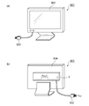
- FIGS. 7A and 7B are diagrams illustrating an electronic device 900 including the switching regulator 2.
- 7A and 7B is a display device, but the type of the electronic device 900 is not particularly limited, and is a device including a power supply device such as an audio device, a refrigerator, a washing machine, or a vacuum cleaner. I just need it.
- Plug 902 receives a commercial AC voltage V AC from the wall outlet (not shown).
- a rectifier circuit that converts an AC voltage into a DC voltage is provided in the preceding stage of the switching regulator 2.
- the switching regulator 2 receives a DC voltage from the rectifier circuit.
- the switching regulator 2 is mounted in the housing 804.
- the DC output voltage V OUT generated by the switching regulator 2 is supplied to loads such as a microcomputer, a DSP (Digital Signal Processor), a power supply circuit, a lighting device, an analog circuit, and a digital circuit mounted in the same housing 904.
- the DSP Digital Signal Processor
- SYMBOLS 100 Control circuit, 2 ... Switching regulator, 4 ... Rectifier circuit, 6 ... PFC circuit, 8 ... Load, L1 ... Inductor, C2 ... Input capacitor, C1 ... Output capacitor, Rs ... Current detection resistor, D1 ... Rectifier diode, 102 DESCRIPTION OF SYMBOLS ... Feedback circuit, M1 ... Switching transistor, OUT ... Switching terminal, FB ... Feedback terminal, CS ... Current detection terminal, GND ... Ground terminal, 10 ... Current limiting comparator, 12 ... Oscillator, 14 ... Mask signal generator, 20 ... Reset signal generator, 22 ... Slope generator, 24 ... Adder, 26 ...
- Error comparator 30 ... Pulse signal generator, 32 ... SR flip-flop, 34 ... First AND gate, 36 ... First inverter, 38 ... OR gate , 39 ... second AND gate, 40 ... driver, 42, 4 ... dead time generating section, 46 ... second inverter, 48 ... third inverter, P1 ... input terminal, P2 ... output terminal.
- the present invention relates to a non-insulated step-down switching regulator (DC / DC converter).
Landscapes
- Engineering & Computer Science (AREA)
- Power Engineering (AREA)
- Dc-Dc Converters (AREA)
Abstract
Description
dIL/dt=VL/L …(1)
スイッチングトランジスタM1がオンのとき、インダクタL1の一端には、入力電圧VINが印加され、その他端は、出力端子の地絡により0Vが印加される。したがって、オン時間TMSKごとに、コイル電流ILは、式(2)で与えられる電流量ΔION増大する。
ΔION=TMSK×VIN/L …(2)
ΔIOFF=TOFF×VF/L …(3)
入力電圧VIN=141V、VF=0.6Vとすると、ΔION>ΔIOFFが成り立つため、サイクル毎にコイル電流ILが増大し、やがて回路の信頼性に影響を及ぼすことになる。
スイッチングレギュレータの出力端子が地絡するなどして、出力電圧が低下すると、インダクタに流れるコイル電流が次第に増大し、電流制限用コンパレータにより過電流状態が検出される。電流制限用コンパレータが生成する電流制限信号は、オン期間、オフ期間を問わずに、継続的にアサートされ続ける。そして、この電流制限信号によってセット信号をマスクすることにより、スイッチングトランジスタが第1レベルに遷移しなくなるため、スイッチングトランジスタをオフに保つことができ、コイル電流が上昇し続けるのを防止できる。その結果、回路の信頼性を改善できる。
本発明のさらに別の態様は、ACアダプタである。このACアダプタは、上述のスイッチングレギュレータを備える。
同様に、「部材Cが、部材Aと部材Bの間に設けられた状態」とは、部材Aと部材C、あるいは部材Bと部材Cが直接的に接続される場合のほか、それらの電気的な接続状態に実質的な影響を及ぼさない、あるいはそれらの結合により奏される機能や効果を損なわせない、その他の部材を介して間接的に接続される場合も含む。
電子機器1は、たとえばテレビや冷蔵庫、エアコンなどの家電製品やコンピュータである。電子機器1は、スイッチングレギュレータ2、整流回路4、PFC(力率改善)回路6、負荷8を備える。
スイッチング端子OUTは、スイッチングトランジスタM1の制御端子(ゲート)と接続される。スイッチングトランジスタM1はNチャンネルMOSFETであり、それをオンするためには、ゲートソース間にMOSFETのしきい値電圧を超える駆動電圧を印加する必要がある。そこで制御回路100の接地端子GNDは、検出抵抗RsとインダクタL1の接続点N1と接続される。
制御回路100は、電流制限用コンパレータ10、オシレータ12、マスク信号生成部14、リセット信号生成部20、パルス信号生成部30、ドライバ40を備え、ピーク電流モードでスイッチングトランジスタM1のスイッチングを制御する。
オシレータ12は、所定の周期ごとにアサート(ハイレベル)されるセット信号SSETを生成する。
エラーコンパレータ26は、加算器24によってスロープ信号SSLOPEが重畳された検出電圧Vs’を、フィードバック電圧VFBと比較する。そして、検出電圧Vsがフィードバック電圧VFBより高くなるとアサート(ハイレベル)されるセット信号SSETを生成する。リセット信号生成部20の構成は特に限定されず、別の構成としてもよい。
第1インバータ36は、電流制限信号SLIMを反転する。第1ANDゲート34には、セット信号SSETと第1インバータ36の出力信号が入力される。第1ANDゲート34の出力信号は、SRフリップフロップ32のセット端子(S)に入力される。
セット信号SSETが所定の周期ごとにアサートされるごとに、パルス信号SPWMがハイレベルとなり、スイッチングトランジスタM1がオンする。スイッチングトランジスタM1がオンすると、コイル電流ILが上昇に転ずる。検出電圧Vsがフィードバック電圧VFBに達すると、リセット信号SRSTがアサートされ、パルス信号SPWMがローレベルとなり、スイッチングトランジスタM1がオフする。
出力電圧VOUTが低下すると、コイル電流ILが増大し、それにともなって検出電圧Vsが増大する。時刻t1に検出電圧Vsがしきい値電圧VTHを超えると、電流制限信号SLIMがアサートされる。電流制限信号SLIMがアサートされると、パルス信号SPWMがローレベルとなり、スイッチングトランジスタM1がオフする。
プラグ902、図示しないコンセントから商用交流電圧VACを受ける。スイッチングレギュレータ2の前段には、交流電圧を直流電圧に変換する整流回路が設けられる。スイッチングレギュレータ2は、整流回路からの直流電圧を受ける。スイッチングレギュレータ2は、筐体804内に実装される。スイッチングレギュレータ2により生成された直流出力電圧VOUTは、同じ筐体904内に搭載される、マイコン、DSP(Digital Signal Processor)、電源回路、照明機器、アナログ回路、デジタル回路などの負荷に供給される。
Claims (10)
- 入力端子に入力電圧を受け、出力端子から降圧された出力電圧を出力するスイッチングレギュレータの制御回路であって、
前記スイッチングレギュレータは、
前記入力端子と前記出力端子の間に順に直列に設けられたスイッチングトランジスタ、検出抵抗およびインダクタと、
前記スイッチングトランジスタと前記検出抵抗の接続点と接地端子の間に設けられた整流ダイオードと、
前記出力端子と接地端子の間に設けられた出力キャパシタと、を含み、
前記制御回路は、
前記スイッチングトランジスタの制御端子と接続されるべきスイッチング端子と、
前記スイッチングトランジスタと前記検出抵抗の接続点と接続されるべき電流検出端子と、
前記検出抵抗と前記インダクタの接続点と接続されるべき接地端子と、
前記出力電圧に応じたフィードバック電圧が入力されるべきフィードバック端子と、
前記検出端子の検出電圧が、所定のしきい値電圧より高いときにアサートされる電流制限信号を生成する電流制限用コンパレータと、
所定の周期ごとにアサートされるセット信号を生成するオシレータと、
前記スイッチングトランジスタがオンした後、所定の遅延時間経過後にアサートされるマスク信号を生成するマスク信号生成部と、
前記フィードバック電圧に応じてアサートされるタイミングが調節されるリセット信号を生成するリセット信号生成部と、
前記スイッチングトランジスタがオンすべき期間に第1レベル、オフすべき期間に第2レベルとなるパルス信号を生成するパルス信号生成部であって、(a)前記電流制限信号がネゲートされる期間に前記セット信号がアサートされると、前記パルス信号を前記第1レベルに遷移させ、(b)前記リセット信号がアサートされると、または前記マスク信号がネゲートされる期間に前記電流制限信号がアサートされると、前記パルス信号を前記第2レベルに遷移させるパルス信号生成部と、
前記パルス信号に応じたスイッチング信号を、前記スイッチング端子を介して前記スイッチングトランジスタの前記制御端子に出力するドライバと、
を備えることを特徴とする制御回路。 - 前記パルス信号生成部は、
前記電流制限信号を反転する第1インバータと、
前記セット信号と前記第1インバータの出力が入力される第1ANDゲートと、
そのセット端子に、前記セット信号に応じた前記第1ANDゲートの出力信号が入力され、そのリセット端子に、前記リセット信号に応じた信号が入力されるSRフリップフロップと、
を備えることを特徴とする請求項1に記載の制御回路。 - 前記マスク信号と前記電流制限信号が入力される第2ANDゲートと、
前記リセット信号と前記第2ANDゲートの出力信号が入力されるORゲートと、
をさらに備え、
前記SRフリップフロップの前記リセット端子には、前記リセット信号に応じた前記ORゲートの出力信号が入力されることを特徴とする請求項2に記載の制御回路。 - 前記パルス信号生成部は、
前記マスク信号と前記電流制限信号が入力される第2ANDゲートと、
前記リセット信号と前記第2ANDゲートの出力信号が入力されるORゲートと、
そのセット端子に、前記セット信号に応じた信号が入力され、そのリセット端子に、前記リセット信号に応じた前記ORゲートの出力信号が入力されるSRフリップフロップと、
を備えることを特徴とする請求項1に記載の制御回路。 - 前記リセット信号生成部は、
前記検出電圧を前記フィードバック電圧と比較し、前記検出電圧が前記フィードバック電圧より高くなるとアサートされる前記セット信号を生成するエラーコンパレータを含むことを特徴とする請求項1から4のいずれかに記載の制御回路。 - 前記リセット信号生成部は、
前記セット信号と同期した三角波またはのこぎり波のスロープ信号を生成するスロープ生成部と、
前記検出電圧と前記スロープ信号を加算する加算器と、
をさらに含むことを特徴とする請求項5に記載の制御回路。 - 前記マスク信号生成部は、前記パルス信号に応じた信号を、遅延させる遅延回路を含むことを特徴とする請求項1から6のいずれかに記載の制御回路。
- 入力端子に入力電圧を受け、出力端子から降圧された出力電圧を出力するスイッチングレギュレータであって、
前記入力端子と前記出力端子の間に順に直列に設けられたスイッチングトランジスタ、検出抵抗およびインダクタと、
前記スイッチングトランジスタと前記検出抵抗の接続点と接地端子の間に設けられた整流ダイオードと、
前記出力端子と接地端子の間に設けられた出力キャパシタと、
前記スイッチングトランジスタを駆動する請求項1から7のいずれかに記載の制御回路と、
を備えることを特徴とするスイッチングレギュレータ。 - 請求項8に記載のスイッチングレギュレータを備えることを特徴とする電子機器。
- 請求項8に記載のスイッチングレギュレータを備えることを特徴とするACアダプタ。
Priority Applications (3)
| Application Number | Priority Date | Filing Date | Title |
|---|---|---|---|
| JP2013514990A JP5952809B2 (ja) | 2011-05-13 | 2012-05-14 | 非絶縁降圧スイッチングレギュレータおよびその制御回路、電子機器、acアダプタ |
| CN201280027580.2A CN103597721B (zh) | 2011-05-13 | 2012-05-14 | 非绝缘降压开关稳压器及其控制电路、电子设备、ac适配器 |
| US14/079,111 US8837181B2 (en) | 2011-05-13 | 2013-11-13 | Step down switching regulator |
Applications Claiming Priority (2)
| Application Number | Priority Date | Filing Date | Title |
|---|---|---|---|
| JP2011-108423 | 2011-05-13 | ||
| JP2011108423 | 2011-05-13 |
Related Child Applications (1)
| Application Number | Title | Priority Date | Filing Date |
|---|---|---|---|
| US14/079,111 Continuation US8837181B2 (en) | 2011-05-13 | 2013-11-13 | Step down switching regulator |
Publications (1)
| Publication Number | Publication Date |
|---|---|
| WO2012157242A1 true WO2012157242A1 (ja) | 2012-11-22 |
Family
ID=47176594
Family Applications (1)
| Application Number | Title | Priority Date | Filing Date |
|---|---|---|---|
| PCT/JP2012/003125 Ceased WO2012157242A1 (ja) | 2011-05-13 | 2012-05-14 | 非絶縁降圧スイッチングレギュレータおよびその制御回路、電子機器、acアダプタ |
Country Status (4)
| Country | Link |
|---|---|
| US (1) | US8837181B2 (ja) |
| JP (1) | JP5952809B2 (ja) |
| CN (1) | CN103597721B (ja) |
| WO (1) | WO2012157242A1 (ja) |
Cited By (2)
| Publication number | Priority date | Publication date | Assignee | Title |
|---|---|---|---|---|
| JP2016092956A (ja) * | 2014-11-04 | 2016-05-23 | ローム株式会社 | スイッチングコンバータおよびその制御回路、制御方法、それを用いた照明装置、電子機器 |
| US10243344B2 (en) | 2015-09-29 | 2019-03-26 | Rohm Co., Ltd. | Semiconductor device |
Families Citing this family (8)
| Publication number | Priority date | Publication date | Assignee | Title |
|---|---|---|---|---|
| JP5757785B2 (ja) * | 2011-05-19 | 2015-07-29 | ローム株式会社 | 電源装置およびそれを用いた電子機器 |
| JP6578128B2 (ja) * | 2015-05-14 | 2019-09-18 | ローム株式会社 | 電力供給装置、acアダプタ、acチャージャ、電子機器および電力供給システム |
| JP6620013B2 (ja) * | 2015-12-25 | 2019-12-11 | ローム株式会社 | スイッチング電源装置 |
| US10291134B2 (en) * | 2016-08-29 | 2019-05-14 | Silanna Asia Pte Ltd | Switching mode power supply with an anti-windup circuit including a voltage clamping circuit |
| JP6762431B2 (ja) * | 2017-07-31 | 2020-09-30 | ローム株式会社 | 電流検出回路 |
| CN107526423A (zh) * | 2017-08-30 | 2017-12-29 | 安徽天达网络科技有限公司 | 一种计算机通断电自保护控制系统 |
| US10122272B1 (en) * | 2017-12-30 | 2018-11-06 | Active-Semi, Inc. | Cycle skipping prevent circuit in a regulator of a DC-to-DC converter |
| TWI796013B (zh) * | 2021-11-26 | 2023-03-11 | 通嘉科技股份有限公司 | 電源轉換器的電源控制器與控制方法 |
Citations (3)
| Publication number | Priority date | Publication date | Assignee | Title |
|---|---|---|---|---|
| JP2008104285A (ja) * | 2006-10-18 | 2008-05-01 | Ac Technologies Kk | スイッチング電源方式 |
| JP2008199705A (ja) * | 2007-02-08 | 2008-08-28 | Toyota Motor Corp | 電流モード型スイッチング電源 |
| JP2009278756A (ja) * | 2008-05-14 | 2009-11-26 | Rohm Co Ltd | スイッチングレギュレータ |
Family Cites Families (7)
| Publication number | Priority date | Publication date | Assignee | Title |
|---|---|---|---|---|
| US6101106A (en) * | 1999-02-05 | 2000-08-08 | The Boeing Company | Pulse width modulated controller for high temperature power conversion |
| US6608450B2 (en) * | 2000-06-13 | 2003-08-19 | Lighttech Group, Inc. | High frequency, high efficiency electronic lighting system with sodium lamp |
| US6819011B2 (en) * | 2002-11-14 | 2004-11-16 | Fyre Storm, Inc. | Switching power converter controller with watchdog timer |
| US6781352B2 (en) * | 2002-12-16 | 2004-08-24 | International Rectifer Corporation | One cycle control continuous conduction mode PFC boost converter integrated circuit with integrated power switch and boost converter |
| JP4980588B2 (ja) * | 2005-06-21 | 2012-07-18 | ローム株式会社 | 降圧型スイッチングレギュレータ、その制御回路、ならびにそれを用いた電子機器 |
| US7560909B2 (en) * | 2005-11-14 | 2009-07-14 | Asahi Kasei Microsystems Co., Ltd. | Power converter using extrapolative conductance mode control |
| JP5211678B2 (ja) * | 2007-12-26 | 2013-06-12 | 富士通セミコンダクター株式会社 | Dc−dcコンバータ、dc−dcコンバータの制御方法および電子機器 |
-
2012
- 2012-05-14 WO PCT/JP2012/003125 patent/WO2012157242A1/ja not_active Ceased
- 2012-05-14 JP JP2013514990A patent/JP5952809B2/ja active Active
- 2012-05-14 CN CN201280027580.2A patent/CN103597721B/zh active Active
-
2013
- 2013-11-13 US US14/079,111 patent/US8837181B2/en active Active
Patent Citations (3)
| Publication number | Priority date | Publication date | Assignee | Title |
|---|---|---|---|---|
| JP2008104285A (ja) * | 2006-10-18 | 2008-05-01 | Ac Technologies Kk | スイッチング電源方式 |
| JP2008199705A (ja) * | 2007-02-08 | 2008-08-28 | Toyota Motor Corp | 電流モード型スイッチング電源 |
| JP2009278756A (ja) * | 2008-05-14 | 2009-11-26 | Rohm Co Ltd | スイッチングレギュレータ |
Cited By (2)
| Publication number | Priority date | Publication date | Assignee | Title |
|---|---|---|---|---|
| JP2016092956A (ja) * | 2014-11-04 | 2016-05-23 | ローム株式会社 | スイッチングコンバータおよびその制御回路、制御方法、それを用いた照明装置、電子機器 |
| US10243344B2 (en) | 2015-09-29 | 2019-03-26 | Rohm Co., Ltd. | Semiconductor device |
Also Published As
| Publication number | Publication date |
|---|---|
| JP5952809B2 (ja) | 2016-07-13 |
| CN103597721A (zh) | 2014-02-19 |
| JPWO2012157242A1 (ja) | 2014-07-31 |
| US8837181B2 (en) | 2014-09-16 |
| US20140218988A1 (en) | 2014-08-07 |
| CN103597721B (zh) | 2016-02-17 |
Similar Documents
| Publication | Publication Date | Title |
|---|---|---|
| JP5952809B2 (ja) | 非絶縁降圧スイッチングレギュレータおよびその制御回路、電子機器、acアダプタ | |
| JP6122257B2 (ja) | Dc/dcコンバータおよびその制御回路、それを用いた電源装置、電源アダプタおよび電子機器 | |
| JP6220249B2 (ja) | スイッチングコンバータおよびその制御回路、ac/dcコンバータ、電源アダプタおよび電子機器 | |
| JP5785710B2 (ja) | Dc/dcコンバータならびにそれを用いた電源装置および電子機器 | |
| JP5977950B2 (ja) | Dc/dcコンバータおよびその制御回路、それを用いた電源装置、電源アダプタおよび電子機器 | |
| JP6469481B2 (ja) | 絶縁同期整流型dc/dcコンバータ、2次側コントローラ、それを用いた電源装置、電源アダプタおよび電子機器 | |
| JP6563651B2 (ja) | 絶縁同期整流型dc/dcコンバータ、同期整流コントローラ、それを用いた電源装置、電源アダプタおよび電子機器 | |
| JP6410554B2 (ja) | スイッチングコンバータおよびその制御回路、ac/dcコンバータ、電源アダプタおよび電子機器 | |
| JP6382059B2 (ja) | スイッチング電源回路 | |
| CN101557166A (zh) | 电源设备和半导体集成电路器件 | |
| JP2012257444A (ja) | 昇圧型スイッチングレギュレータの制御回路およびそれを用いたスイッチングレギュレータならびに電子機器 | |
| JP2012161117A (ja) | Dc/dcコンバータならびにそれを用いた電源装置および電子機器 | |
| JP6039274B2 (ja) | Dc/dcコンバータおよびその制御回路、それを用いた電源装置、電源アダプタおよび電子機器 | |
| JP2017118767A (ja) | 力率改善回路およびその制御回路、制御方法、電子機器、電源アダプタ | |
| JP2017093159A (ja) | 降圧dc/dcコンバータおよびその制御回路、制御方法、車載用電源装置 | |
| JP2013062947A (ja) | Dc/dcコンバータならびにそれを用いた電源装置および電子機器 | |
| JP2018129907A (ja) | Dc/dcコンバータおよびその制御回路、制御方法、車載電装機器 | |
| JP2016116415A (ja) | 絶縁型のdc/dcコンバータ、それを用いた電源装置、電源アダプタおよび電子機器、1次側コントローラ | |
| JP6356545B2 (ja) | スイッチング電源装置 | |
| JP2017225248A (ja) | 絶縁型のdc/dcコンバータ、それを用いた電源アダプタおよび電子機器 | |
| JP2018007515A (ja) | 絶縁型のdc/dcコンバータならびにその一次側コントローラ、制御方法、それを用いた電源アダプタおよび電子機器 | |
| JP2016116414A (ja) | 絶縁型のdc/dcコンバータ、それを用いた電源装置、電源アダプタおよび電子機器、フィードバックアンプ集積回路 | |
| JP2018007357A (ja) | Dc/dcコンバータおよびその制御回路、インダクタのショート検出方法、制御方法、電子機器 | |
| JP2018099021A (ja) | 非絶縁型のdc/dcコンバータおよびそのコントローラ、電子機器 | |
| US10230301B2 (en) | Non-isolated DC/DC converter |
Legal Events
| Date | Code | Title | Description |
|---|---|---|---|
| WWE | Wipo information: entry into national phase |
Ref document number: 201280027580.2 Country of ref document: CN |
|
| 121 | Ep: the epo has been informed by wipo that ep was designated in this application |
Ref document number: 12786506 Country of ref document: EP Kind code of ref document: A1 |
|
| ENP | Entry into the national phase |
Ref document number: 2013514990 Country of ref document: JP Kind code of ref document: A |
|
| NENP | Non-entry into the national phase |
Ref country code: DE |
|
| 122 | Ep: pct application non-entry in european phase |
Ref document number: 12786506 Country of ref document: EP Kind code of ref document: A1 |