WO2012157449A1 - Dispositif à semi-conducteur, module de cellule solaire, chaîne de cellules solaires et réseau de cellules solaires - Google Patents
Dispositif à semi-conducteur, module de cellule solaire, chaîne de cellules solaires et réseau de cellules solaires Download PDFInfo
- Publication number
- WO2012157449A1 WO2012157449A1 PCT/JP2012/061547 JP2012061547W WO2012157449A1 WO 2012157449 A1 WO2012157449 A1 WO 2012157449A1 JP 2012061547 W JP2012061547 W JP 2012061547W WO 2012157449 A1 WO2012157449 A1 WO 2012157449A1
- Authority
- WO
- WIPO (PCT)
- Prior art keywords
- solar cell
- semiconductor
- photoelectric conversion
- layer
- substrate
- Prior art date
- Legal status (The legal status is an assumption and is not a legal conclusion. Google has not performed a legal analysis and makes no representation as to the accuracy of the status listed.)
- Ceased
Links
Images


Classifications
-
- H—ELECTRICITY
- H10—SEMICONDUCTOR DEVICES; ELECTRIC SOLID-STATE DEVICES NOT OTHERWISE PROVIDED FOR
- H10F—INORGANIC SEMICONDUCTOR DEVICES SENSITIVE TO INFRARED RADIATION, LIGHT, ELECTROMAGNETIC RADIATION OF SHORTER WAVELENGTH OR CORPUSCULAR RADIATION
- H10F19/00—Integrated devices, or assemblies of multiple devices, comprising at least one photovoltaic cell covered by group H10F10/00, e.g. photovoltaic modules
- H10F19/90—Structures for connecting between photovoltaic cells, e.g. interconnections or insulating spacers
- H10F19/902—Structures for connecting between photovoltaic cells, e.g. interconnections or insulating spacers for series or parallel connection of photovoltaic cells
-
- H—ELECTRICITY
- H10—SEMICONDUCTOR DEVICES; ELECTRIC SOLID-STATE DEVICES NOT OTHERWISE PROVIDED FOR
- H10F—INORGANIC SEMICONDUCTOR DEVICES SENSITIVE TO INFRARED RADIATION, LIGHT, ELECTROMAGNETIC RADIATION OF SHORTER WAVELENGTH OR CORPUSCULAR RADIATION
- H10F19/00—Integrated devices, or assemblies of multiple devices, comprising at least one photovoltaic cell covered by group H10F10/00, e.g. photovoltaic modules
- H10F19/30—Integrated devices, or assemblies of multiple devices, comprising at least one photovoltaic cell covered by group H10F10/00, e.g. photovoltaic modules comprising thin-film photovoltaic cells
- H10F19/31—Integrated devices, or assemblies of multiple devices, comprising at least one photovoltaic cell covered by group H10F10/00, e.g. photovoltaic modules comprising thin-film photovoltaic cells having multiple laterally adjacent thin-film photovoltaic cells deposited on the same substrate
- H10F19/33—Patterning processes to connect the photovoltaic cells, e.g. laser cutting of conductive or active layers
-
- H—ELECTRICITY
- H10—SEMICONDUCTOR DEVICES; ELECTRIC SOLID-STATE DEVICES NOT OTHERWISE PROVIDED FOR
- H10F—INORGANIC SEMICONDUCTOR DEVICES SENSITIVE TO INFRARED RADIATION, LIGHT, ELECTROMAGNETIC RADIATION OF SHORTER WAVELENGTH OR CORPUSCULAR RADIATION
- H10F19/00—Integrated devices, or assemblies of multiple devices, comprising at least one photovoltaic cell covered by group H10F10/00, e.g. photovoltaic modules
- H10F19/30—Integrated devices, or assemblies of multiple devices, comprising at least one photovoltaic cell covered by group H10F10/00, e.g. photovoltaic modules comprising thin-film photovoltaic cells
- H10F19/31—Integrated devices, or assemblies of multiple devices, comprising at least one photovoltaic cell covered by group H10F10/00, e.g. photovoltaic modules comprising thin-film photovoltaic cells having multiple laterally adjacent thin-film photovoltaic cells deposited on the same substrate
- H10F19/35—Structures for the connecting of adjacent photovoltaic cells, e.g. interconnections or insulating spacers
-
- H—ELECTRICITY
- H10—SEMICONDUCTOR DEVICES; ELECTRIC SOLID-STATE DEVICES NOT OTHERWISE PROVIDED FOR
- H10F—INORGANIC SEMICONDUCTOR DEVICES SENSITIVE TO INFRARED RADIATION, LIGHT, ELECTROMAGNETIC RADIATION OF SHORTER WAVELENGTH OR CORPUSCULAR RADIATION
- H10F77/00—Constructional details of devices covered by this subclass
- H10F77/93—Interconnections
- H10F77/933—Interconnections for devices having potential barriers
- H10F77/935—Interconnections for devices having potential barriers for photovoltaic devices or modules
-
- Y—GENERAL TAGGING OF NEW TECHNOLOGICAL DEVELOPMENTS; GENERAL TAGGING OF CROSS-SECTIONAL TECHNOLOGIES SPANNING OVER SEVERAL SECTIONS OF THE IPC; TECHNICAL SUBJECTS COVERED BY FORMER USPC CROSS-REFERENCE ART COLLECTIONS [XRACs] AND DIGESTS
- Y02—TECHNOLOGIES OR APPLICATIONS FOR MITIGATION OR ADAPTATION AGAINST CLIMATE CHANGE
- Y02E—REDUCTION OF GREENHOUSE GAS [GHG] EMISSIONS, RELATED TO ENERGY GENERATION, TRANSMISSION OR DISTRIBUTION
- Y02E10/00—Energy generation through renewable energy sources
- Y02E10/50—Photovoltaic [PV] energy
- Y02E10/541—CuInSe2 material PV cells
-
- Y—GENERAL TAGGING OF NEW TECHNOLOGICAL DEVELOPMENTS; GENERAL TAGGING OF CROSS-SECTIONAL TECHNOLOGIES SPANNING OVER SEVERAL SECTIONS OF THE IPC; TECHNICAL SUBJECTS COVERED BY FORMER USPC CROSS-REFERENCE ART COLLECTIONS [XRACs] AND DIGESTS
- Y02—TECHNOLOGIES OR APPLICATIONS FOR MITIGATION OR ADAPTATION AGAINST CLIMATE CHANGE
- Y02P—CLIMATE CHANGE MITIGATION TECHNOLOGIES IN THE PRODUCTION OR PROCESSING OF GOODS
- Y02P70/00—Climate change mitigation technologies in the production process for final industrial or consumer products
- Y02P70/50—Manufacturing or production processes characterised by the final manufactured product
Definitions
- the present invention relates to a semiconductor device, a solar cell module, a solar cell string, and a solar cell array, and more particularly, in a semiconductor device, a semiconductor element having improved insulation between a conductive substrate made of a conductive material and a semiconductor element.
- the present invention relates to an arrangement method and a solar cell module, a solar cell string, and a solar cell array using the semiconductor element.
- a substrate made of a conductive material such as a metal or alloy having the characteristics of lightness and flexibility may be applicable to a wide range of applications. Further, since the substrate made of the conductive material can withstand high temperature processes, it can be applied to a semiconductor that cannot be handled by a resin substrate such as polyimide. For example, if it is used as a substrate for a solar cell, the photoelectric conversion efficiency can be improved, and high efficiency of the solar cell can be expected.
- an insulating layer is provided on at least one surface of a substrate made of a conductive material.
- an oxide obtained by anodizing a substrate material is used (for example, Patent Document 1).
- Patent Document 1 discloses that the potential in the vicinity of the middle of series-connected elements (that is, solar cells) and the potential of the substrate made of a conductive material (metal substrate) are made equipotential. Accordingly, it is disclosed that the potential difference between the element and the substrate is reduced.
- FIGS. 7A and 7B show the results of simulating the state of electrolytic concentration at the electrode corners.
- FIG. 7A shows the result when the curvature of the corner is changed
- FIG. 7B shows the result when the angle of the corner is changed. From FIG. 7A, it can be seen that the electric field E max at the electrode end portion having a diameter of 25 mm (corresponding to the electrode corner portion having a curvature radius of 12.5 mm) is about 1.3 times the electric field E 0 at the center portion of the electrode.
- Patent Document 4 discloses that a wiring arrangement is devised for the problem of reducing the planar distribution of a potential difference between wirings on a substrate.
- the method disclosed in Patent Document 4 does not disclose a method for adjusting the potential between the semiconductor element and the wiring and the substrate when the substrate is made of a conductive material, the method is applied as it is.
- the insulation with the substrate cannot be improved.
- An object of the present invention is to eliminate the problems based on the prior art and to provide a semiconductor device with excellent insulation withstand voltage between a plurality of semiconductor elements provided on a conductive substrate made of a conductive material and the conductive substrate. It aims at providing a solar cell module, a solar cell string, and a solar cell array.
- a first aspect of the present invention includes a conductive substrate made of a conductive material, a nonconductive layer made of a nonconductive material provided on at least a part of the surface of the substrate, A plurality of semiconductor elements provided on the non-conductive layer; wiring that electrically connects the semiconductor elements; a conductive substrate; and at least one electrical connection portion that connects the semiconductor element or the wiring.
- the semiconductor element having the maximum potential difference from the conductive substrate is arranged at a position excluding a geometric end of an array formed by a plurality of semiconductor elements.
- the geometric end means, for example, when an array formed by a plurality of semiconductor elements is one line segment, as shown in FIG.
- the semiconductor element 51a including the apex is indicated.
- the geometric end indicates a semiconductor element 51a including a vertex of a polygon when the array formed by the plurality of semiconductor elements 51 is a polygon.
- the geometric end refers to the semiconductor element 51a including the vertex when the shape of the semiconductor element 51 is a polygon, as shown in FIG. 1D.
- the semiconductor element 51a including the circumference is indicated. Regardless of the shape of one semiconductor element, in the present invention, the semiconductor element 51a including any of the above-described elements is defined as a geometric end.
- the electrical connection portion is, for example, a mechanical contact portion that presses against a part of a semiconductor element to press it, an alloyed joint portion such as soldering, and the corresponding portion is heated and melted. Welding parts and the like. Further, even if the substrate and the semiconductor element are not in contact with each other, the potential of the semiconductor element with respect to the substrate is substantially reduced, for example, there is a thin insulating layer and there is a semiconductor property. The part that can be determined is also included in the electrical connection. The potential difference between the conductive substrate (conductive material portion) and the semiconductor element is adjusted by the electrical connection portion. Each semiconductor element is connected in series or in parallel by wiring, whereby the potential difference distribution between the conductive substrate and the semiconductor element or wiring is adjusted.
- the semiconductor element in contact with the electrical connection portion is preferably arranged in a range of 10% of the number of the plurality of semiconductor elements from at least one end of the array, and more preferably, the plurality of semiconductor elements from at least one end of the array It is characterized in that it is at least one semiconductor element which is arranged in the range of 5% of the number of and which are equipotential to each other.
- the semiconductor element is particularly preferably a semiconductor element disposed at at least one end of the array. Since the vicinity of the end of the array is equipotential with the conductive material portion, the potential difference at the end can be reduced. By reducing the potential difference around the end portion, the electric field concentration is alleviated and the overall insulation is enhanced.
- the nonconductive layer is formed by anodizing a conductive substrate, and at least one semiconductor having a maximum potential among a plurality of semiconductor elements.
- the element is in contact with the electrical connection.
- the anodic oxide film has higher insulating properties when the base metal side is the positive electrode.
- the semiconductor element having the maximum potential and the conductive substrate (conductive material portion) are equipotential, the conductive substrate (conductive material portion) is always the positive electrode, so that the overall insulation is improved.
- the conductive substrate a lightweight and flexible substrate made of titanium or aluminum is preferable, and an inexpensive substrate made of aluminum is more preferable.
- a composite aluminum substrate made of a composite material is preferable instead of a substrate made of aluminum.
- the composite material includes, for example, a material in which a resin or another metal is combined with aluminum.
- a clad substrate made of a steel plate or a stainless steel plate and an aluminum plate is more preferable because it can improve the heat resistance of aluminum.
- the plurality of semiconductor elements are concentrically arranged, and at least one semiconductor element having the maximum potential difference from the conductive substrate is disposed at the center of the concentric arrangement. It is characterized by being arranged.
- the electric field concentration is mitigated by the concentric arrangement, and the potential difference between the conductive substrate and at least one semiconductor element that maximizes the potential difference with the conductive substrate is located farthest from the end of the arrangement.
- the electric field in the direction parallel to is reduced, and the overall insulation is improved.
- a semiconductor device is characterized in that a plurality of semiconductor elements are arranged on a straight line, and two arrays connected in series are connected in parallel.
- the manufacturing process is not increased, and by connecting two series circuits in parallel, the output voltage is halved, so that the required withstand voltage can be halved.
- the semiconductor element having the maximum potential difference with respect to the substrate is disposed at a position excluding the geometric end of the array formed by the semiconductor elements, the electric field concentration point is reduced and the insulation can be improved.
- the output voltage can be reduced to 1/4, 1/8,. Can be lowered.
- the two arrays have the maximum potential difference between the semiconductor elements located at both ends of the arrays and the connection parts of the arrays, but the semiconductor elements that have the maximum potential difference with the conductive substrate are not disposed at both ends of the arrays. Therefore, the potential difference between the semiconductor element or the wiring located at the connection part of the two arrays and the conductive substrate is maximized, and the insulation between the geometric end of the array where the electric field concentration is likely to occur and the conductive substrate is achieved. As a result, the overall insulation is improved.
- the semiconductor device which was excellent in the insulation voltage resistance between the some semiconductor element provided on a conductive substrate and a conductive substrate can be provided.
- a high-performance device can be made by increasing the number of semiconductor elements by improving the insulation voltage resistance.
- it can manufacture at low cost by making the thickness of a nonelectroconductive layer thin.
- the insulation at the end portion of the device is improved, the insulation from the periphery of the device is also improved.
- a light and strong conductive frame can be provided around the device.
- the output can be divided into two systems by a parallel circuit, and even when a failure occurs on one half of the device Can maintain half of the output. Further, by increasing the number of parallel circuits, the failure probability can be further lowered and durability can be increased.
- a solar cell module that is connected in series and outputs at a high voltage is preferable as a semiconductor device, and a thin-film type or an integrated type solar cell module that is required to be lightweight and flexible is more preferable. preferable.
- a CIGS solar cell module capable of increasing efficiency is particularly preferable.
- a solar cell string and a solar cell array can be made using these solar cell modules.
- the insulating property is improved, when the same voltage is output, the ineffective area generated at the edge of the substrate can be reduced, the material can be used efficiently, and the cost can be reduced.
- (A) is a schematic diagram which shows the state in which the several photovoltaic cell is arranged on 1 line
- (b) and (c) are the schematics which show the state in which the polygonal photovoltaic cell is arranged. It is a figure and (d) is a schematic diagram which shows a state in case the arrangement
- 1 is a schematic cross-sectional view of a photoelectric conversion device according to a first embodiment of a semiconductor device of the present invention. It is a circuit block diagram of the photoelectric conversion apparatus of 1st Embodiment of the semiconductor device of this invention.
- FIG. 1 It is a typical perspective view of the photoelectric conversion apparatus under manufacture for demonstrating an example of the manufacturing process of the photoelectric conversion apparatus of 1st Embodiment of the semiconductor device of this invention. It is a flowchart which shows an example of the manufacturing method of the photoelectric conversion apparatus of 1st Embodiment of the semiconductor device of this invention. It is typical sectional drawing of the photoelectric conversion apparatus of 2nd Embodiment of the semiconductor device of this invention. (A), (b) shows the result of simulating the state of electrolytic concentration at the electrode corner, (a) shows the result when the curvature of the corner is changed, and (b) shows the corner. The result at the time of changing the angle of a part is shown. It is typical sectional drawing which shows the conventional photoelectric conversion apparatus.
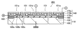
- FIG. 2 is a schematic cross-sectional view of the photoelectric conversion device according to the first embodiment of the semiconductor device of the present invention.
- FIG. 3 is a circuit configuration diagram of the photoelectric conversion device according to the first embodiment of the semiconductor device of the present invention. It is.
- the photoelectric conversion device 201 (solar cell module) of the present invention is formed on, for example, a grounded, substantially rectangular conductive substrate 100 made of a conductive material, and the conductive substrate 100.
- a support substrate 110 (a substrate made of a conductive material + a layer made of a non-conductive material) made of a non-conductive layer (insulating layer) 130 made of a non-conductive material, and a photoelectric substrate formed on the non-conductive layer 130. It has the electric power generation layer 140 which consists of the several photovoltaic cell 151 (photoelectric conversion element) of the converter 201.
- the power generation layer 140 is configured by arranging a plurality of solar cells 151 on a straight line and connecting two arrays connected in series in parallel. In FIG. 2, there are a total of two arrays connected in series on both sides of the central negative electrode, and the two arrays are connected in parallel.
- the photoelectric conversion device 201 of the present invention has a ribbon-shaped lead (not shown) with the positive electrode (plus) side of at least one solar cell 151a at both ends of the plurality of solar cells 151 of the power generation layer 140 as a positive electrode terminal. It is connected to a positive terminal of a contact box (not shown) through a wire, and is grounded by directly electrically connecting to the conductive substrate 100 of the support substrate 110 as a grounding terminal.
- the negative electrode (minus) side of one or two solar cells 151d at the center of the plurality of solar cells 151 is not shown as a negative electrode terminal via a ribbon-shaped lead wire (not shown). It is characterized in that it is connected to the negative terminal of the junction box.
- the conductive substrate 100 of the support substrate 110 is grounded, and its positive electrode is directly electrically connected to the conductive substrate 100 of the support substrate 110.
- the grounding solar cell 151a is grounded via the conductive layer 160, and the grounding solar cell 151a is most preferably a solar cell at both ends of the plurality of solar cells 151.
- the withstand voltage VW1 required with respect to the conductive substrate 100 is approximately the same as the withstand voltage Vw1d required from the potential difference V1d.
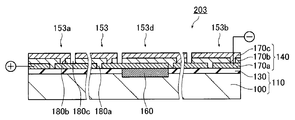
- the photoelectric conversion device 203 corresponds to the solar cell module 10 of Patent Document 1.
- the photoelectric conversion device 201 of the present embodiment When the number of photovoltaic cells in the photoelectric conversion device 201 of the present embodiment and the conventional photoelectric conversion device 203 are the same, the respective outputs are approximately the same. However, at the peripheral portion of the power generation layer where the required withstand voltage becomes high due to the influence of electric field concentration or creeping discharge, the photoelectric conversion device 201 of this embodiment has two sides at both end portions facing the substrate end of the solar cell 151d. Only the electric potential difference with the conductive substrate 100 becomes the maximum and the electric field concentrates, whereas the conventional photoelectric conversion device 203 has a conductive substrate extending over three sides facing the substrate end of the solar battery cell 153a or 153d.
- the photoelectric conversion device 201 of this embodiment is more advantageous for insulation.
- three sides face the substrate edge, and the other side faces the next cell. Yes.
- the solar cells 151 having the maximum potential difference from the conductive substrate 100 are at both ends of the plurality of solar cells 151 of the power generation layer 140. Since it is arrange
- the position of the grounding solar cell 151 a is at least one solar cell at both ends of the plurality of solar cells 151 of the power generation layer 140.
- the invention is not limited to this, and may be solar cells around both ends of the power generation layer 140. Furthermore, it is good also as at least 1 photovoltaic cell in the range of 10% of the number of the several photovoltaic cells 151 from the both ends of the electric power generation layer 140. The reason is that the solar cells 151 are connected in series from the solar cells 151d to at least one solar cell 151a at both ends among the plurality of solar cells 151 of one power generation layer 140.
- the number of solar cells 151 from the battery cell 151d to one solar cell around both ends is 40% or more of the total.
- the potential difference V1d is four times or more than the potential difference V1c between the solar cells around both ends of the power generation layer 140 and the conductive substrate 100. Therefore, in the photoelectric conversion device 201, the position of the grounding solar cell 151a is changed. This is because the potential difference V1d is the largest among all the solar battery cells 151 in the solar battery cells around both ends as in the case described above.
- the potential difference V1d is nine times Va1. That's it. For this reason, it is more preferable to set it as the at least 1 photovoltaic cell which exists in the range of 10% of the number of several photovoltaic cells 151 from both ends.
- the support substrate 110 used in the illustrated photoelectric conversion device 201 is a metal plate with an insulating layer having the conductive substrate 100 and the nonconductive layer 130 formed thereon.
- the supporting substrate 110 is not particularly limited as long as it is a metal plate with an insulating layer, but at least one surface side of an aluminum (Al) plate is anodized to make the anodized film a non-conductive layer 130. It is preferable that the support substrate 110 is obtained by using an Al plate that is formed and not anodized as the conductive substrate 100.
- the conductive substrate 100 is not particularly limited as long as the non-conductive layer 130 can be formed and the power generation layer 140 can be supported when the support substrate 110 is a metal plate with an insulating layer. Absent.
- the conductive substrate 100 is preferably an Al substrate having an Al layer on at least one surface. Examples thereof include an Al substrate and a composite Al substrate made of a composite material of Al and another metal.
- the thickness is preferably 0.05 to 10 mm.
- the support substrate 110 is manufactured from an Al substrate, a composite Al substrate, or the like, it is necessary to have a thickness that allows for a reduction in thickness due to anodic oxidation, pre-cleaning and polishing of the anodic oxidation.
- the Al substrate may be, for example, a Japanese Industrial Standard (JIS) 1000 series pure Al plate, or an Al alloy plate such as an Al—Mn alloy plate, an Al—Mg alloy plate, An alloy plate of Al and other metal elements such as an Al—Mn—Mg alloy plate, an Al—Zr alloy plate, an Al—Si alloy plate, and an Al—Mg—Si alloy plate may also be used.
- the composite Al substrate includes a clad plate of an Al plate and another metal plate, for example, a clad plate of a stainless steel (SUS) plate, and a clad plate in which various steel plates are sandwiched between two Al plates. Also good.
- the other metal plates constituting the clad plate with the Al plate are various stainless steel plates, for example, steel such as mild steel, 42 Invar alloy, Kovar alloy, or 36 Invar alloy.
- a metal plate that can be used as a roofing material or a wall material of a house or a building can be used so that the photoelectric conversion device of the present invention can be used as a roofing material integrated solar battery panel.
- the Al plate or Al alloy plate used here may contain various trace metal elements such as Fe, Si, Mn, Cu, Mg, Cr, Zn, Bi, Ni, and Ti.
- the nonconductive layer 130 formed on the conductive substrate 100 is not particularly limited.
- the conductive substrate 100 is an Al substrate or a composite Al substrate, it is preferably an anodized film formed on the surface of the Al substrate or the composite Al substrate by anodizing.
- the anodic oxidation of the Al substrate or the composite Al substrate can be performed by using the Al substrate or the composite Al substrate as an anode, immersing it in an electrolytic solution together with a cathode, and applying a voltage between the anode and the cathode to perform an electrolytic treatment.
- the anodic oxide film that becomes the non-conductive layer 130 may be formed on one surface of the Al layer of the Al substrate or the composite Al substrate that becomes the conductive substrate 100.
- the Al substrate or two Al plates may be used.
- the sandwiched clad plate in order to suppress warpage due to the difference in thermal expansion coefficient between the Al layer and the anodic oxide film, cracks generated in the anodic oxide film, etc. It is preferable to provide an anodic oxide film on the surface of the Al layer.
- the thickness of the non-conductive layer 130 thus formed that is, the thickness of the anodized film is not particularly limited.
- the non-conductive layer 130 only needs to have insulation and surface hardness that prevents damage due to mechanical shock during handling.
- the non-conductive layer 130 is too thick, there is a problem in terms of flexibility. There is a case. For this reason, the preferred thickness of the non-conductive layer 130 is 0.5 to 50 ⁇ m.
- the thickness of the non-conductive layer 130 can be controlled by electrolysis time together with constant current electrolysis or constant voltage electrolysis.
- various oxide layers such as glass containing elements such as Si, Ca, Zn, B, P, Ti, etc. in addition to the anodic oxide coating of Al are deposited, sol-gel method, etc. It may be formed by these various methods.
- the photoelectric conversion device 201 of the first embodiment of the present invention shown in FIG. 2 is called a substrate type, and the power generation layer 140 provided in the photoelectric conversion device 201 is of a thin film integrated type.
- the power generation layer 140 is disposed on the non-conductive layer 130 of the support substrate 110 in a straight line adjacent to the grounding solar cells 151a disposed at both ends of the power generation layer 140, and is connected in series. It has a plurality of solar cells 151 connected in parallel.
- the solar battery 151 includes a back electrode 170a formed on the surface of the non-conductive layer 130 of the support substrate 110 in FIG. 8 and a photoelectric conversion layer 170b formed on the back electrode 170a that converts received light into electricity. And a transparent electrode 170c formed on the photoelectric conversion layer 170b, and the back electrode 170a, the photoelectric conversion layer 170b, and the transparent electrode 170c are sequentially stacked on the non-conductive layer 130.
- the grounding solar cell 151a is a feature of the present invention, and a part of the non-conductive layer 130 formed on the support substrate 110 of the solar cell 151 is the conductive layer 160.
- the grounding solar cell 151a may be a cell that contributes to power generation as long as the conductive layer 160 that electrically connects and electrically connects the back electrode 170a and the conductive substrate 100 is formed. It may be a cell that does not contribute to.
- a buffer layer is formed on the photoelectric conversion layer 170b, and the back electrode 170a, the photoelectric conversion layer 170b, the buffer layer, and The transparent electrodes 170c may be sequentially stacked.
- the back electrode 170 a is applied from the region on the end side (a part on the right side in the drawing) of the adjacent (left side in the drawing) solar cell 151 or the grounding solar cell 151 a.
- the non-conductive layer 130 is formed by forming a P1 scribe groove 180a at a predetermined interval from the back surface electrode 170a of the adjacent solar battery cell 151 so as to be arranged in the most area of the solar battery cell 151 (left side in the figure). It is formed on the surface. Also in the grounding solar cell 151a, the back electrode 170a is formed from the region on the end side (a part on the right side in the drawing) of the adjacent (left side in the drawing) adjacent solar cell 151, as in the solar cell 151.
- the conductive layer 160 and the non-conductive layer are formed with a groove 180a at a predetermined interval from the back surface electrode 170a of the adjacent solar battery cell 151 so as to be arranged in the most area of the grounding solar battery cell 151a (left side in the figure). It is formed on the surface of the layer 130. Most of the back electrode 170 a of the grounding solar cell 151 a is disposed on the conductive layer 160.
- the photoelectric conversion layer 170b is formed on the back electrode 170a so as to fill the groove 180a between the adjacent back electrodes 170a. Therefore, the photoelectric conversion layer 170b is in direct contact with the non-conductive layer 130 and / or the conductive layer 160 at the portion of the groove 180a.
- the photoelectric conversion layer 170b is formed with a P2 scribe groove 180b extending from the adjacent solar cell 151 or the grounding solar cell 151a to the back electrode 170a extending. Therefore, the groove 180b is formed at a position (right side in the drawing) different from the groove 180a between the adjacent back surface electrodes 170a.
- the transparent electrode 170c is formed on the surface of the photoelectric conversion layer 170b so as to fill the groove 180b of the photoelectric conversion layer 170b. Therefore, the transparent electrode 170c is in direct contact with and electrically connected to the back surface electrode 170a of the adjacent solar cell 151 or the grounding solar cell 151a in the groove 180b. Thus, the two adjacent solar cells 151 and the adjacent solar cells 151 and the grounding solar cell 151a are connected in series.
- a groove 180c reaching the back electrode 170a is formed between the transparent electrode 170c and the photoelectric conversion layer 170b of the battery cell 151a.
- the adjacent two solar cells 151 and the adjacent solar cells 151 and the grounding solar cells 151a are separated by the groove 180c.
- the plurality of solar cells 151 and the grounding solar cell 151a are the solar cells 151 or the grounding solar cells 151a adjacent to the transparent electrode 170c of the solar cell 151 or the grounding solar cell 151a. Are connected in series by being connected to the back electrode 170a.
- the back electrodes 170a of the solar cells 151 at both ends are drawn out as positive terminals (+ terminals) by lead wires such as copper ribbons (not shown), and are centered or substantially omitted.
- the transparent electrode 170c of the central solar cell 151 is drawn out as a negative terminal ( ⁇ terminal) by a similar lead wire, and the back electrode 170a of the grounding solar cell 151a at both ends is connected via the grounding solar cell 151a. Then, it is grounded by being electrically connected to the grounded conductive substrate 100.
- the conductive substrate 100 is connected to the ground terminal by a similar lead wire.
- the solar cells 151 and the grounding solar cells 151a are parallel to one side of the rectangular conductive substrate 100 in a direction perpendicular to the cross section shown in FIG. 2 (a direction perpendicular to the paper surface of FIG. 2). It has a strip-like shape formed in an extending line shape. Accordingly, the back electrode 170 a and the transparent electrode 170 c are similarly strip-shaped electrodes that are long in one direction parallel to the side of the conductive substrate 100.
- the solar cell 151 of this embodiment is called an integrated CIGS solar cell (CIGS photoelectric conversion element).
- the back electrode 170a is a molybdenum electrode
- the photoelectric conversion layer 170b is CIGS
- the electrode 170c is made of ZnO.
- the buffer layer is formed, it is composed of CdS.
- the grounding solar battery 151a has the same configuration.
- such solar cells 151 and grounding solar cells 151a can be manufactured by, for example, a known CIGS solar cell manufacturing method. Further, in order to separate the groove 180a between the back electrode 170a, the groove 180b reaching the back electrode 170a formed in the photoelectric conversion layer 170b, the photoelectric conversion layer 170b, and the transparent electrode from the adjacent photoelectric conversion layer 170b and the transparent electrode. Line-shaped groove portions such as the groove 180c reaching the back electrode 170a can be formed by laser scribe or mechanical scribe.
- the photoelectric conversion device 201 of this embodiment when light is incident on the solar cell 151 and the grounding solar cell 151a from the transparent electrode 170c side, the light passes through the transparent electrode 170c and the buffer layer (not shown). When it passes through and reaches the photoelectric conversion layer 170b, an electromotive force is generated. For example, a current from the transparent electrode 170c toward the back electrode 170a is generated. Note that the arrows shown in FIG. 2 indicate the direction of current, and the direction of movement of electrons is opposite to the direction of current. Therefore, in FIG. 2, the back electrode 170a of the left end solar cell 151 is a positive electrode (+ electrode), and the transparent electrode 170c of the right end solar cell 151 is a negative electrode ( ⁇ electrode).
- the back electrode 170a and the transparent electrode 170c are for taking out the current generated in the photoelectric conversion layer 170b. Both the back electrode 170a and the transparent electrode 170c are made of a conductive material. The transparent electrode 170c on the light incident side needs to have translucency.
- the back electrode 170a is made of, for example, Mo, Cr, or W and a combination thereof.
- the back electrode 170a may have a single layer structure or a laminated structure such as a two-layer structure.
- the back electrode 170a preferably has a thickness of 100 nm or more, and more preferably 0.45 to 1.0 ⁇ m.
- the method for forming the back electrode 170a is not particularly limited, and can be formed by a vapor deposition method such as an electron beam evaporation method or a sputtering method.
- the transparent electrode 170c is made of, for example, ZnO, ITO (indium tin oxide), SnO 2 or a combination thereof.
- the transparent electrode 170c may have a single layer structure or a laminated structure such as a two-layer structure. Further, the thickness of the transparent electrode 170c is not particularly limited, and is preferably 0.3 to 1 ⁇ m.
- the method for forming the transparent electrode 170c is not particularly limited, and can be formed by a vapor deposition method such as an electron beam evaporation method or a sputtering method.
- An antireflection film such as MgF 2 may be formed on the transparent electrode 170c.
- the buffer layer is formed to protect the photoelectric conversion layer 170b when the transparent electrode 170c is formed and to transmit light incident on the transparent electrode 170c to the photoelectric conversion layer 170b.
- This buffer layer is made of, for example, CdS, ZnS, ZnO, ZnMgO, ZnS (O, OH), or a combination thereof.
- the buffer layer preferably has a thickness of 0.03 to 0.1 ⁇ m.
- the buffer layer is formed by, for example, a CBD (chemical bath) method, a solution growth method, or the like. Note that a high resistance film made of ZnO or the like may be formed between the buffer layer such as CBD-CdS and the transparent electrode 170c such as ZnO: Al.
- the photoelectric conversion layer 170b is a layer that generates current by absorbing light that has passed through the transparent electrode 170c and the buffer layer.
- the configuration of the photoelectric conversion layer 170b is not particularly limited, and is preferably, for example, at least one compound semiconductor having a chalcopyrite structure.
- the photoelectric conversion layer 170b may be at least one compound semiconductor composed of a group Ib element, a group IIIb element, and a group VIb element.
- the photoelectric conversion layer 170b includes at least one type Ib group element selected from the group consisting of Cu and Ag, and a group consisting of Al, Ga, and In.
- this compound semiconductor CuAlS 2 , CuGaS 2 , CuInS 2 , CuAlSe 2 , CuGaSe 2 , CuInSe 2 (CIS), AgAlS 2 , AgGaS 2 , AgInS 2 , AgAlSe 2 , AgGaSe 2 , AgInSe 2 , AgInSe 2 , AgInSe 2 , AgInSe 2 , AgInSe 2 , AgInT , AgInTe 2 , Cu (In 1-x Ga x ) Se 2 (CIGS), Cu (In 1-x Al x ) Se 2 , Cu (In 1-x Ga x ) (S, Se) 2 , Ag (In 1-x Gax) Se 2 , Ag (In 1-x Ga x ) (S, Se) 2 and
- the photoelectric conversion layer 170b particularly preferably includes CuInSe 2 (CIS) and / or Cu (In, Ga) Se 2 (CIGS) in which Ga is dissolved.
- CIS and CIGS are semiconductors having a chalcopyrite crystal structure, have high light absorption, and high photoelectric conversion efficiency has been reported. Moreover, there is little degradation of efficiency by light irradiation etc. and it is excellent in durability.
- the photoelectric conversion layer 170b contains impurities for obtaining a desired semiconductor conductivity type. Impurities can be contained in the photoelectric conversion layer 170b by diffusion from adjacent layers and / or active doping.
- the constituent elements and / or impurities of the I-III-VI group semiconductor may have a concentration distribution, and a plurality of layer regions having different semiconductor properties such as n-type, p-type, and i-type May be included.
- the band gap width / carrier mobility and the like can be controlled, and the photoelectric conversion efficiency can be designed high.
- the photoelectric conversion layer 170b may contain one or more semiconductors other than the group I-III-VI semiconductor.
- semiconductors other than I-III-VI group semiconductors include semiconductors composed of group IVb elements such as Si (group IV semiconductors), semiconductors composed of group IIIb elements such as GaAs and group Vb elements (group III-V semiconductors), and Examples thereof include semiconductors composed of IIb group elements such as CdTe and VIb group elements (II-VI group semiconductors).
- the photoelectric conversion layer 170b may contain an arbitrary component other than a semiconductor and impurities for obtaining a desired conductivity type as long as the characteristics are not hindered.
- the content of the I-III-VI group semiconductor in the photoelectric conversion layer 170b is not particularly limited.
- the content of the group I-III-VI semiconductor in the photoelectric conversion layer 170b is preferably 75% by mass or more, more preferably 95% by mass or more, and particularly preferably 99% by mass or more.
- the CIGS layer may be formed by 1) a multi-source co-evaporation method, 2) a selenization method (selenization / sulfurization method), or 3) a sputtering method. 4) a hybrid sputtering method, and 5) a mechanochemical process method are known.
- the selenization method is also called a two-step method.
- a metal precursor of a laminated film such as a Cu layer / In layer or a (Cu—Ga) layer / In layer is sputtered, vapor deposited, or electrodeposited.
- a selenium compound such as Cu (In 1-x Ga x ) Se 2 is produced by a thermal diffusion reaction by heating the film to 450 to 550 ° C. in selenium vapor or hydrogen selenide. is there.
- This method is called a vapor phase selenization method.
- there is a solid-phase selenization method in which solid-phase selenium is deposited on a metal precursor film and selenized by a solid-phase diffusion reaction using the solid-phase selenium as a selenium source.
- a Cu—Ga alloy film is first deposited, an In film is deposited thereon, and when this is selenized, natural thermal diffusion is used to form Ga.
- a method of inclining the concentration in the film thickness direction K. Kushiya et.al, Tech.Digest 9th Photovoltaic Science and Engineering Conf.Miyazaki, 1996 (Intn.
- a sputtering method As a sputtering method, a method using CuInSe 2 polycrystal as a target, a two-source sputtering method using Cu 2 Se and In 2 Se 3 as a target and using a H 2 Se / Ar mixed gas as a sputtering gas (J. Ermer, et.al, Proc. 18th IEEE Photospecifics Conf. (1985) 1655-1658., Etc.), and a three-source sputtering method in which a Cu target, an In target, and a Se or CuSe target are sputtered in Ar gas (T Nakada, et.al, Jpn.J.Appl.Phys.32 (1993) L1169-L1172, etc.).
- CIGS film formation methods include screen printing, proximity sublimation, MOCVD, and spraying.
- a fine particle film containing an Ib group element, an IIIb group element, and a VIb group element is formed on a substrate by a screen printing method or a spray method, etc.
- Japanese Patent Laid-Open No. 9-74065 and Japanese Patent Laid-Open No. 9-74213 are examples of Japanese Patent Laid-Open No. 9-74065 and Japanese Patent Laid-Open No. 9-74213).
- the solar cells 151 and the grounding solar cells 151a of the photoelectric conversion device 201 (solar cell module) of the first embodiment described above are integrated CIGS solar cells, but the present invention is limited to this.
- the configuration of the solar cell and the photoelectric conversion element, particularly the photoelectric conversion layer, functioning as the solar cell of the photoelectric conversion device (solar cell module) of the present invention is, for example, an amorphous silicon (a-Si) solar cell Cell, tandem solar cell (a-Si / a-SiGe tandem solar cell), series connection (SCAF) solar cell (a-Si serial connection solar cell), CdTe (cadmium tellurium) )
- Solar cell III-V solar cell, thin-film silicon solar cell, dye-sensitized solar cell, or organic solar cell It may be me, even what is referred to as a substrate type, may be what is called a super straight type.
- the back electrode 170a side is the positive electrode (+ electrode) and the transparent electrode 170c side is the negative electrode ( ⁇ electrode).
- the present invention is not limited to this, and the solar cell Depending on the cell, the back electrode 170a side may be the negative electrode ( ⁇ electrode) and the transparent electrode 170c side may be the positive electrode (+ electrode).
- a tandem solar cell (a-Si / a-SiGe tandem solar cell) is used as the solar cell 151 and the grounding solar cell 151a, for example, Ag
- the transparent electrode 170c is made of ITO
- the photoelectric conversion layer 170b is made of an intrinsic semiconductor layer such as an n-type semiconductor layer, microcrystalline silicon, and amorphous silicon germanium (a-SiGe).
- a p-type semiconductor layer is stacked, and an n-type semiconductor layer, an intrinsic semiconductor layer such as amorphous silicon (a-Si), and a photoelectric conversion layer on which a p-type semiconductor layer is stacked can be used.
- a photoelectric conversion layer called a CdTe (cadmium tellurium) type is used as the photoelectric conversion layer 170b. it can.
- the conductive layer 160 of the grounding solar cell 151a will be described.
- the conductive layer 160 is the most characteristic part of the present invention, and is disposed in place of the nonconductive layer 130 between the conductive substrate 100 and the back electrode 170a in the grounding solar cell 151a.
- the back electrode 170a having conductivity is electrically connected to the grounded conductive substrate 100 to be conductive and grounded.
- the conductive layer 160 is a mixture of the component of the conductive substrate 100, the component of the non-conductive layer 130, and the component of the back electrode 170a. As a result, the conductive layer 160 has conductivity. .
- the conductive layer 160 is formed only on the lower portion of the back electrode 170a of the grounding solar cell 151a, and is not formed on the lower portion of the groove 180a and is nonconductive.
- the present invention is not limited to this, and the lower portion of the groove 180a and the lower portion of the back electrode 170a of the adjacent solar cell 151 are provided in the grounding solar cell 151a.
- the conductive layer 160 may be used. However, in this case, since the back electrode 170a of the grounding solar cell 151a and the back electrode 170a of the adjacent solar cell 151 are short-circuited, the grounding solar cell 151a does not contribute to power generation.
- such a conductive layer 160 is obtained by applying ultrasonic solder 190 on the transparent electrode 170 c of the solar battery cell 151 to be the grounding solar battery cell 151 a and applying the ultrasonic solder 190.
- the nonconductive layer 130 corresponding to the portion where the ultrasonic solder 190 of the solar cell 151a is applied is destroyed and the nonconductive material is destroyed.
- the surfaces of the conductive substrate 100 and the back electrode 170a that have been in contact with the layer 130 are dissolved and mixed, and the conductive substrate 100, the back electrode 170a, and the broken non-conductive layer 130 are mixed to form. be able to.
- the formation of the mixed state of the conductive layer 14 is not particularly clarified, for example, only the solar battery cell 151a to which the ultrasonic solder 190 is applied is subjected to the heating ultrasonic treatment, whereby the solar battery cell 151a.
- the non-conductive layer 130 corresponding to the portion to which the ultrasonic solder 190 is applied is broken to create a fine void to be porous, and the conductive substrate that is in contact with the broken non-conductive layer 130 It is presumed that a mixed state is formed by entering the fine voids of the non-conductive layer 130 that is broken by melting the surfaces of the 100 and the back electrode 170a.
- the conductive layer 160 mixed with these and the ultrasonic solder 190 may be formed.
- the solder may be applied to the entire surface of the grounding solar cell 151a, but the transparent electrode 170c may be left partly as shown in FIG.
- soldering may be performed in a linear manner while supplying solder onto the cell without applying solder, but soldering may be performed on the wire at a time after placing the solder, or a plurality of linear locations may be provided. Soldering at the same time is preferable for production.
- the conductivity of the conductive layer 160 formed in this way is considered to be determined by the mixed state of the conductive layer 160. Therefore, the configuration or function of the solar cell 151 to be the grounding solar cell 151a and Depending on the necessity of the power generation function, especially the thickness of the non-conductive layer 130, etc., the amount of ultrasonic solder 190 applied, the heating temperature, the heating time, the ultrasonic strength and the ultrasonic processing time, etc. Can be controlled by appropriately controlling the required electric conductivity.
- the conductivity of the conductive layer 160, the configuration and function of the solar cell 151, particularly the thickness of the non-conductive layer 130, the coating amount of the ultrasonic solder 190, the heating temperature in the heating ultrasonic treatment, the heating time, the ultrasonic wave The relationship between the strength and the sonication time may be obtained in advance by experiments or simulations.
- the conductive layer 160 is formed as described above. However, the present invention is not limited to this, and if the non-conductive layer 130 is formed on the substrate 101 made of a conductive material, You may form in any step of manufacture of a photoelectric conversion apparatus.
- the non-conductive layer 130 on the conductive substrate 100 is coated with ultrasonic solder on a corresponding portion to be the grounding solar cell 151a and subjected to heating ultrasonic treatment, and the broken non-conductive layer 130 and A conductive layer 160 in which the conductive substrate 100 and ultrasonic solder are mixed may be formed, and then a plurality of solar cells 151 and grounding solar cells 151a may be formed.
- ultrasonic solder is applied to the back electrode 170a corresponding to the ground solar cell 151a, and heating ultrasonic treatment is performed.
- the conductive layer 160 in which the broken non-conductive layer 130, the conductive substrate 100, and the back electrode 170a are mixed, or the conductive layer 160 in which ultrasonic solder is also mixed is formed, and sequentially,
- the photoelectric conversion layer 170b and the transparent electrode 170c may be formed to form a plurality of solar cells 151 and grounding solar cells 151a. Further, after forming the photoelectric conversion layer 170b, the conductive layer 160 is formed in the same manner, and the transparent electrode 170c is formed thereon to form a plurality of solar cells 151 and grounding solar cells 151a. May be.
- the solar battery cell 151 since the solar battery cell 151 is completed after forming the conductive layer 160, it is necessary to form one or more of the back electrode 170a, the photoelectric conversion layer 170b, and the transparent electrode 170c. Therefore, since accurate alignment is required, it is preferable to form the conductive layer 160 after forming the solar cells 151.
- FIG. 5 is a flowchart showing an example of a method of manufacturing the photoelectric conversion device according to the first embodiment of the present invention shown in FIG.
- the anodic oxidation treatment is performed by the above-described method to form an anodic oxide film that becomes the non-conductive layer 130 on the surface, thereby having the anodic oxide film.
- An Al substrate is formed and prepared as a support substrate 110 (step S100).
- an Al substrate having an anodized film may be prepared in advance as the support substrate 110.
- Mo is deposited on the non-conductive layer 130 of the support substrate 110 by a known film formation method such as the DC magnetron sputtering method described above to form a Mo film (step S102).
- the Mo film thus formed on the non-conductive layer 130 is cut by the laser scribing method described above, and is patterned into the pattern 1 to form the groove 180a, thereby forming the back electrode 170a (step S104).
- the photoelectric conversion layer 170b and the photoelectric conversion layer 170b are formed by a known method such as the above-described selenization / sulfurization method or multi-source co-evaporation method so as to fill the groove 180a on the back electrode 170a formed on the non-conductive layer 130.
- a CIGS compound semiconductor film (p-type CIGS light absorption film) is formed (step S106). Subsequently, a CdS film (n-type high resistance buffer layer) to be a buffer layer is formed on the CIGS compound semiconductor film thus formed by a known method such as CBD described above (step S108).
- the CIGS compound semiconductor film and the CdS film thus formed on the back electrode 170a are integrally cut by the mechanical scribing method described above, and patterned into the pattern 2 to form the groove 180b reaching the back electrode 170a. Then, the photoelectric conversion layer 170b and the buffer layer are formed (step S110).
- a ZnO film (n-type ZnO) that becomes the transparent electrode 170c by a known method such as the above-described MOCVD method or RF sputtering method so as to fill the groove 180b on the buffer layer (photoelectric conversion layer 170b) thus formed.
- a transparent conductive film window layer is formed (step S112).
- the ZnO film, the buffer layer, and the photoelectric conversion layer 170b thus formed are integrated, cut by the mechanical scribing method described above, and patterned into the pattern 3, and between the adjacent solar cells 151, the back electrode 170a.
- the solar cell 151 is separated into the photoelectric conversion layer 170b, the buffer layer, and the transparent electrode 170c to form a plurality of solar cells 151 (step S114).
- the ultrasonic solder 190 is applied on the transparent electrode 170c of the solar battery cell 151 to be the preset grounding solar battery cell 151a (step S116).
- the transparent electrode 170c of the solar battery cell 151 to which the ultrasonic solder 190 is applied is selectively subjected to heating ultrasonic treatment, and the non-conductive layer 130 is broken to remove the component and the component of the conductive substrate 100.
- the conductive layer 160 is formed by mixing the components of the back electrode 170a (step S118).
- the photoelectric conversion device 201 of the present embodiment is formed (step S118).
- FIG. 6 is a schematic cross-sectional view of the photoelectric conversion device 202 (solar cell module) of the second embodiment of the semiconductor device of the present invention.
- the photoelectric conversion apparatus 202 of this embodiment shown in FIG. 6 and the photoelectric conversion apparatus 201 of 1st Embodiment shown in FIG. 1 differ except the structure of the conductive layer 160 of the photovoltaic cell 151a for grounding.
- the same components are denoted by the same reference numerals, and detailed description thereof is omitted.
- the photoelectric conversion device 202 of this embodiment extends from an adjacent solar cell 151 instead of the conductive layer 160 of the grounding solar cell 151 a of the photoelectric conversion device 201 of the first embodiment.
- the existing back electrode 170a is directly disposed between the conductive substrate 100 and the photoelectric conversion layer 170b to form the conductive layer 160. Therefore, in the photoelectric conversion device 202 of the present embodiment, the back electrode 170a and the grounded conductive substrate 100 are in direct contact and are electrically connected, so that the back electrode 170a of the grounding solar cell 151a is electrically conductive. It can be grounded through the conductive substrate 100.
- the solar cell 151 and the grounding solar cell 151a have any configuration. Of course, it may be (photoelectric conversion element, photoelectric conversion layer).
- the non-conductive layer 130 such as the anodic oxide film is not formed only in the portion corresponding to the grounding solar cell 151a, and the anodic oxide film is formed in the other portions.
- the power generation layer 140 is formed using the support substrate 110 made of the conductive substrate 100 such as an Al substrate on which the non-conductive layer 130 such as is formed. That is, the back electrode 170a and the conductive layer 160, the photoelectric conversion layer 170b and the buffer layer, and the transparent electrode 170c are sequentially formed, and a plurality of solar cells 151 and a grounding solar cell 151a are formed. be able to.
- the photoelectric conversion device 202 of this embodiment can be formed.
- the entire surface of the conductive substrate 100 such as an anodized Al substrate is used instead of the support substrate 110 made of the conductive substrate 100 in which the nonconductive layer 130 is not formed only on the portion corresponding to the grounding solar cell 151a.
- the support substrate 110 in a state where the nonconductive layer 130 such as the anodized film corresponding to the ground solar cell 151a of the support substrate 110 on which the nonconductive layer 130 is formed is removed by scribing or etching is used.
- the photovoltaic layer 202 of this embodiment may be formed by forming the power generation layer 140 starting from the deposition of the back electrode 170a.
- both the photoelectric conversion device 201 (solar cell module) of the first embodiment and the photoelectric conversion device 202 (solar cell module) of the second embodiment may include a conductive frame.
- this conductive frame in order to place the solar cell module on a roof base material such as a base plate or a waterproof underlaying material, the peripheral edge of the solar cell module, that is, the ridge side, the eaves side, the left side, It is a member for a solar cell module attached to the right edge.
- the conductive frame an aluminum frame suitable for workability and environmental resistance is mainly used.
- both the photoelectric conversion device 201 (solar cell module) of the first embodiment and the photoelectric conversion device 202 (solar cell module) of the second embodiment may be connected in series to form a solar cell string. Furthermore, it is good also as a solar cell array by connecting this solar cell string in parallel.
- the photoelectric conversion device 201 of the first embodiment the photoelectric conversion device 202 of the second embodiment, the conventional photoelectric conversion device 203, and the solar cell described in FIG. Compare modules 50.
- a photoelectric conversion device capable of outputting 100 W can be obtained.
- the photoelectric conversion device 201 according to the first embodiment, the photoelectric conversion device 202 according to the second embodiment, the conventional photoelectric conversion device 203, and the solar described in FIG. 7 of Patent Document 1 as a general photoelectric conversion device.
- the ends X11 and X12 of one or two solar cells at the center of the plurality of solar cells, the ends of two solar cells at both ends of the plurality of solar cells Part X21, X22, X23, X24, potential difference VX11, VX12, VX21 between the solar battery cell and the conductive substrate at each point of the central part X31, X32 of the two solar battery cells at both ends of the plurality of solar battery cells VX22, VX23, VX24, VX31, and VX32 are shown in Table 1 below.
- the photoelectric converter 201 has a small potential difference between each solar cell and the conductive substrate. Therefore, since the withstand voltage VW required between the power generation layer and the conductive substrate can be reduced, the insulation withstand voltage can be improved.
- the grounding solar cells 151a are arranged around both ends of the power generation layer 140 in the photoelectric conversion devices 201 according to the first and second embodiments.
- the remaining solar cells 151 are arranged in a straight line adjacent to this, and two arrays connected in series are connected in parallel, so that the solar cell 151d is included in all the solar cells 151.
- the solar cell 151 has the largest potential difference V1d with respect to the conductive substrate 100. Therefore, since the withstand voltage VW is reduced, the insulation is improved and the insulation withstand voltage is excellent.
- the present invention is basically configured as described above. As described above, the photoelectric conversion device has been described in detail as an example of the semiconductor device of the present invention. However, the present invention is not limited to the above-described embodiment, and various improvements or modifications can be made without departing from the gist of the present invention. Of course it is also good.
Landscapes
- Photovoltaic Devices (AREA)
- Physics & Mathematics (AREA)
- Geometry (AREA)
Abstract
L'invention concerne un dispositif à semi-conducteur comportant un substrat conducteur constitué d'un matériau conducteur, une couche non conductrice disposée sur au moins une partie de la surface du substrat conducteur, une pluralité d'éléments semi-conducteurs disposés sur cette couche non conductrice, un câblage qui connecte électriquement la pluralité d'éléments semi-conducteurs et au moins une partie de connexion électrique située entre la couche non conductrice et les éléments semi-conducteurs ou le câblage. L'élément semi-conducteur pour lequel la différence de potentiel par rapport au substrat conducteur est la plus grande est disposé dans une partie autre que l'extrémité géométrique de l'agencement créé par la pluralité d'éléments semi-conducteurs.
Priority Applications (3)
| Application Number | Priority Date | Filing Date | Title |
|---|---|---|---|
| KR1020137029869A KR20140037839A (ko) | 2011-05-13 | 2012-05-01 | 반도체 장치, 태양 전지 모듈, 태양 전지 스트링 및 태양 전지 어레이 |
| CN201280022934.4A CN103548151A (zh) | 2011-05-13 | 2012-05-01 | 半导体装置、太阳电池模块、太阳电池串及太阳电池阵列 |
| US14/078,026 US20140060617A1 (en) | 2011-05-13 | 2013-11-12 | Semiconductor device, solar cell module, solar cell string, and solar cell array |
Applications Claiming Priority (2)
| Application Number | Priority Date | Filing Date | Title |
|---|---|---|---|
| JP2011107995A JP2012238789A (ja) | 2011-05-13 | 2011-05-13 | 半導体装置、太陽電池モジュール、太陽電池ストリングおよび太陽電池アレイ |
| JP2011-107995 | 2011-05-13 |
Related Child Applications (1)
| Application Number | Title | Priority Date | Filing Date |
|---|---|---|---|
| US14/078,026 Continuation US20140060617A1 (en) | 2011-05-13 | 2013-11-12 | Semiconductor device, solar cell module, solar cell string, and solar cell array |
Publications (1)
| Publication Number | Publication Date |
|---|---|
| WO2012157449A1 true WO2012157449A1 (fr) | 2012-11-22 |
Family
ID=47176784
Family Applications (1)
| Application Number | Title | Priority Date | Filing Date |
|---|---|---|---|
| PCT/JP2012/061547 Ceased WO2012157449A1 (fr) | 2011-05-13 | 2012-05-01 | Dispositif à semi-conducteur, module de cellule solaire, chaîne de cellules solaires et réseau de cellules solaires |
Country Status (5)
| Country | Link |
|---|---|
| US (1) | US20140060617A1 (fr) |
| JP (1) | JP2012238789A (fr) |
| KR (1) | KR20140037839A (fr) |
| CN (1) | CN103548151A (fr) |
| WO (1) | WO2012157449A1 (fr) |
Families Citing this family (8)
| Publication number | Priority date | Publication date | Assignee | Title |
|---|---|---|---|---|
| JP6239954B2 (ja) * | 2013-11-28 | 2017-11-29 | 中外炉工業株式会社 | 成膜方法、絶縁基板の製造方法、及びモジュール |
| US20160111556A1 (en) * | 2014-10-15 | 2016-04-21 | Solstice Power LLC | High temperature solar cell mount |
| CN104716219B (zh) * | 2015-02-15 | 2017-12-08 | 深圳先进技术研究院 | 光伏材料及其制备方法 |
| JP6030176B2 (ja) * | 2015-03-19 | 2016-11-24 | 株式会社東芝 | 光電変換素子とその製造方法 |
| JP6943713B2 (ja) * | 2017-09-29 | 2021-10-06 | 積水化学工業株式会社 | 太陽電池 |
| WO2019180854A1 (fr) | 2018-03-20 | 2019-09-26 | 株式会社 東芝 | Module de cellules solaires multijonctions et système de production d'énergie solaire |
| WO2025022532A1 (fr) * | 2023-07-24 | 2025-01-30 | 株式会社東芝 | Structure de cellule solaire connectée |
| WO2025084392A1 (fr) * | 2023-10-19 | 2025-04-24 | 株式会社カネカ | Module de cellules solaires |
Citations (5)
| Publication number | Priority date | Publication date | Assignee | Title |
|---|---|---|---|---|
| JPS614446U (ja) * | 1984-06-13 | 1986-01-11 | 株式会社 半導体エネルギ−研究所 | 薄膜太陽電池 |
| JPH03165579A (ja) * | 1989-11-24 | 1991-07-17 | Sanyo Electric Co Ltd | 光起電力装置およびそれを用いた発光パネル |
| JP2007035695A (ja) * | 2005-07-22 | 2007-02-08 | Kaneka Corp | 集積型薄膜太陽電池モジュール |
| JP2011035270A (ja) * | 2009-08-04 | 2011-02-17 | Sharp Corp | 光電変換装置 |
| JP2011077149A (ja) * | 2009-09-29 | 2011-04-14 | Fujifilm Corp | 太陽電池モジュール |
Family Cites Families (2)
| Publication number | Priority date | Publication date | Assignee | Title |
|---|---|---|---|---|
| JPS62111480A (ja) * | 1985-11-09 | 1987-05-22 | Sanyo Electric Co Ltd | 光起電力装置 |
| JPH1126786A (ja) * | 1997-07-04 | 1999-01-29 | Citizen Watch Co Ltd | 集積型光発電素子 |
-
2011
- 2011-05-13 JP JP2011107995A patent/JP2012238789A/ja not_active Abandoned
-
2012
- 2012-05-01 KR KR1020137029869A patent/KR20140037839A/ko not_active Ceased
- 2012-05-01 WO PCT/JP2012/061547 patent/WO2012157449A1/fr not_active Ceased
- 2012-05-01 CN CN201280022934.4A patent/CN103548151A/zh active Pending
-
2013
- 2013-11-12 US US14/078,026 patent/US20140060617A1/en not_active Abandoned
Patent Citations (5)
| Publication number | Priority date | Publication date | Assignee | Title |
|---|---|---|---|---|
| JPS614446U (ja) * | 1984-06-13 | 1986-01-11 | 株式会社 半導体エネルギ−研究所 | 薄膜太陽電池 |
| JPH03165579A (ja) * | 1989-11-24 | 1991-07-17 | Sanyo Electric Co Ltd | 光起電力装置およびそれを用いた発光パネル |
| JP2007035695A (ja) * | 2005-07-22 | 2007-02-08 | Kaneka Corp | 集積型薄膜太陽電池モジュール |
| JP2011035270A (ja) * | 2009-08-04 | 2011-02-17 | Sharp Corp | 光電変換装置 |
| JP2011077149A (ja) * | 2009-09-29 | 2011-04-14 | Fujifilm Corp | 太陽電池モジュール |
Also Published As
| Publication number | Publication date |
|---|---|
| JP2012238789A (ja) | 2012-12-06 |
| US20140060617A1 (en) | 2014-03-06 |
| CN103548151A (zh) | 2014-01-29 |
| KR20140037839A (ko) | 2014-03-27 |
Similar Documents
| Publication | Publication Date | Title |
|---|---|---|
| US8415557B2 (en) | Photoelectric conversion device and solar cell using the photoelectric conversion device | |
| US20140060617A1 (en) | Semiconductor device, solar cell module, solar cell string, and solar cell array | |
| JP2018157176A (ja) | 太陽電池モジュール及び太陽光発電システム | |
| JP5901773B2 (ja) | 直列接続部を含む薄膜ソーラーモジュール、及び、複数の薄膜ソーラーセルを直列接続する方法 | |
| US20110214708A1 (en) | Solar cell module and solar cell device | |
| US20120279556A1 (en) | Photovoltaic Power-Generating Apparatus and Method For Manufacturing Same | |
| JP2013510426A (ja) | 太陽電池及びその製造方法 | |
| EP2485272A2 (fr) | Appareil de génération d'énergie solaire et son procédé de fabrication | |
| JP4612731B1 (ja) | 太陽電池モジュール | |
| US10134932B2 (en) | Solar cell and method of fabricating the same | |
| JP2011077301A (ja) | 太陽電池モジュール | |
| JP2011077229A (ja) | 光電変換装置 | |
| US9379266B2 (en) | Solar cell module and method of fabricating the same | |
| US20140000703A1 (en) | Thin Film Article and Method for Forming a Reduced Conductive Area in Transparent Conductive Films for Photovoltaic Modules | |
| US9640685B2 (en) | Solar cell and method of fabricating the same | |
| JP5624153B2 (ja) | 太陽電池及びその製造方法 | |
| JP2013026339A (ja) | 薄膜太陽電池およびその製造方法 | |
| JP2017059828A (ja) | 光電変換素子および太陽電池 | |
| JP2011077252A (ja) | 太陽電池モジュール | |
| JP2014007236A (ja) | 集積化太陽電池およびその製造方法 | |
| US20120000529A1 (en) | Method and system for forming a photovoltaic cell and a photovoltaic cell | |
| KR20140080897A (ko) | 태양전지 모듈 및 이의 제조방법 | |
| US20260082708A1 (en) | Solar cell, multijunction solar cell, solar cell module, solar power generation system, and method for manufacturing solar cell | |
| JP5860765B2 (ja) | 光電変換素子および光電変換素子の製造方法 | |
| JP2016157808A (ja) | 光電変換装置 |
Legal Events
| Date | Code | Title | Description |
|---|---|---|---|
| 121 | Ep: the epo has been informed by wipo that ep was designated in this application |
Ref document number: 12784902 Country of ref document: EP Kind code of ref document: A1 |
|
| ENP | Entry into the national phase |
Ref document number: 20137029869 Country of ref document: KR Kind code of ref document: A |
|
| NENP | Non-entry into the national phase |
Ref country code: DE |
|
| 122 | Ep: pct application non-entry in european phase |
Ref document number: 12784902 Country of ref document: EP Kind code of ref document: A1 |