WO2012160624A1 - Procédé pour former un film isolant - Google Patents
Procédé pour former un film isolant Download PDFInfo
- Publication number
- WO2012160624A1 WO2012160624A1 PCT/JP2011/061656 JP2011061656W WO2012160624A1 WO 2012160624 A1 WO2012160624 A1 WO 2012160624A1 JP 2011061656 W JP2011061656 W JP 2011061656W WO 2012160624 A1 WO2012160624 A1 WO 2012160624A1
- Authority
- WO
- WIPO (PCT)
- Prior art keywords
- substrate
- insulating film
- heating
- ultraviolet irradiation
- forming method
- Prior art date
- Legal status (The legal status is an assumption and is not a legal conclusion. Google has not performed a legal analysis and makes no representation as to the accuracy of the status listed.)
- Ceased
Links
Images


Classifications
-
- H—ELECTRICITY
- H10—SEMICONDUCTOR DEVICES; ELECTRIC SOLID-STATE DEVICES NOT OTHERWISE PROVIDED FOR
- H10P—GENERIC PROCESSES OR APPARATUS FOR THE MANUFACTURE OR TREATMENT OF DEVICES COVERED BY CLASS H10
- H10P14/00—Formation of materials, e.g. in the shape of layers or pillars
- H10P14/60—Formation of materials, e.g. in the shape of layers or pillars of insulating materials
- H10P14/66—Formation of materials, e.g. in the shape of layers or pillars of insulating materials characterised by the type of materials
- H10P14/668—Formation of materials, e.g. in the shape of layers or pillars of insulating materials characterised by the type of materials the materials being characterised by the deposition precursor materials
- H10P14/6681—Formation of materials, e.g. in the shape of layers or pillars of insulating materials characterised by the type of materials the materials being characterised by the deposition precursor materials the precursor containing a compound comprising Si
- H10P14/6687—Formation of materials, e.g. in the shape of layers or pillars of insulating materials characterised by the type of materials the materials being characterised by the deposition precursor materials the precursor containing a compound comprising Si the compound comprising silicon and nitrogen
- H10P14/6689—Formation of materials, e.g. in the shape of layers or pillars of insulating materials characterised by the type of materials the materials being characterised by the deposition precursor materials the precursor containing a compound comprising Si the compound comprising silicon and nitrogen the compound being a silazane
-
- H—ELECTRICITY
- H10—SEMICONDUCTOR DEVICES; ELECTRIC SOLID-STATE DEVICES NOT OTHERWISE PROVIDED FOR
- H10P—GENERIC PROCESSES OR APPARATUS FOR THE MANUFACTURE OR TREATMENT OF DEVICES COVERED BY CLASS H10
- H10P14/00—Formation of materials, e.g. in the shape of layers or pillars
- H10P14/60—Formation of materials, e.g. in the shape of layers or pillars of insulating materials
- H10P14/63—Formation of materials, e.g. in the shape of layers or pillars of insulating materials characterised by the formation processes
- H10P14/6326—Deposition processes
- H10P14/6342—Liquid deposition, e.g. spin-coating, sol-gel techniques or spray coating
-
- H—ELECTRICITY
- H10—SEMICONDUCTOR DEVICES; ELECTRIC SOLID-STATE DEVICES NOT OTHERWISE PROVIDED FOR
- H10P—GENERIC PROCESSES OR APPARATUS FOR THE MANUFACTURE OR TREATMENT OF DEVICES COVERED BY CLASS H10
- H10P14/00—Formation of materials, e.g. in the shape of layers or pillars
- H10P14/60—Formation of materials, e.g. in the shape of layers or pillars of insulating materials
- H10P14/65—Formation of materials, e.g. in the shape of layers or pillars of insulating materials characterised by treatments performed before or after the formation of the materials
- H10P14/6516—Formation of materials, e.g. in the shape of layers or pillars of insulating materials characterised by treatments performed before or after the formation of the materials of treatments performed after formation of the materials
- H10P14/6536—Formation of materials, e.g. in the shape of layers or pillars of insulating materials characterised by treatments performed before or after the formation of the materials of treatments performed after formation of the materials by exposure to radiation, e.g. visible light
- H10P14/6538—Formation of materials, e.g. in the shape of layers or pillars of insulating materials characterised by treatments performed before or after the formation of the materials of treatments performed after formation of the materials by exposure to radiation, e.g. visible light by exposure to UV light
Definitions
- the present invention relates to an insulating film forming method for forming an insulating film on a substrate in a semiconductor device.
- a polymer insulating film such as polyvinylphenol is well known, but there are problems such as insufficient insulating properties and durability.
- SiO 2 used as a gate insulating film in a silicon transistor is known to be very stable and highly reliable.
- a semiconductor device capable of forming an insulating film on a substrate with a low insulating temperature and good insulating characteristics during heat treatment. It is an object of the present invention to provide a method for forming an insulating film.
- An insulating film forming method for a semiconductor device is a coating step of applying a catalyst-containing insulating material solution to a surface of a substrate; a heating step of performing a heat treatment on the substrate after the coating step; After the heating step, the substrate is further subjected to a heat treatment and an ultraviolet irradiation step of irradiating the surface of the substrate with ultraviolet rays to form an insulating film on the substrate.
- the substrate is subjected to heat treatment by heat treatment, and then irradiated with ultraviolet rays.
- the substrate is further heat-treated, and the substrate is irradiated with ultraviolet rays to form an insulating film on the substrate, so that the temperature of the heat treatment in each of the heating step and the ultraviolet ray irradiation step can be made lower than before.
- the insulating characteristics of an insulating film formed to a thickness of 100 nm or more can be improved.
- FIG. 1 shows an insulating film forming method of the present invention.
- the insulating film forming method of FIG. 1 is a method of forming a SiO 2 film.
- the insulating film forming method includes (a) a coating process, (b) a drying process, (c) a heating process, and (d) an ultraviolet irradiation process.
- the substrate 11 is placed on the turntable 12.
- the substrate 11 is made of a glass substrate or a plastic substrate (including a flexible substrate). The substrate 11 is rotated in a direction indicated by an arrow A in FIG.
- a Pd-based catalyst-containing polysilazane solution 13 (catalyst) is formed by spin coating.
- the containing insulating material solution) is applied to the surface of the substrate 11.
- the polysilazane solution 13 is dropped from a syringe 14 located above the rotating substrate 11, and thereby applied to the surface of the substrate 11.
- the reason for using the polysilazane solution 13 is that the conversion reactivity is high and the temperature of the heat treatment can be lowered.
- the hot plate 16 contacts the back surface of the substrate 11 and heats the substrate 11 containing the polysilazane solution 13 in the atmosphere.
- the treatment conditions in this drying step are drying by heating at a temperature of 50 ° C. for 10 minutes. This is executed by controlling the hot plate 16 under these conditions.
- the solvent of the polysilazane solution 13 is removed and a dry film is formed.
- bubbles can be prevented from being generated in the insulating film.
- the dry film 17 is heated by the hot plate 22 in the presence of oxygen in the irradiation chamber 21. Further, the ultraviolet ray 23 a is emitted from the ultraviolet irradiation unit 23 to the dry film 17.
- the treatment condition of this step is ultraviolet irradiation for 2 hours in a heating state at a temperature of 150 ° C.
- the above-described (a) coating step, (b) drying step, (c) heating step, and (d) ultraviolet irradiation step are performed, so The polysilazane solution 13 can be converted into a SiO 2 insulating film. Since the maximum heating temperature of each of the (b) drying step, (c) heating step, and (d) ultraviolet irradiation step is 150 ° C., a plastic substrate can be used as the substrate 11. In addition, since the oxygen content in the formed insulating film is about 40% as will be described later, good insulating characteristics can be obtained.
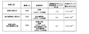
- FIG. 2 shows an actual measurement example of the withstand voltage and the specific resistance as the insulating characteristics of the insulating film in each case where the insulating film forming method is only the heating process, only the ultraviolet irradiation process, and heating process + ultraviolet irradiation process. .
- the film thickness is 200 nm and the heating temperature in each step is 150 ° C.
- the total processing time is 2 hours 30 minutes, but in the case of only the heating process of 3 hours or the same 3 hours of ultraviolet irradiation process Compared with the case of only the above, the withstand voltage and the specific resistance are 6.1 MV / cm and 1.3 ⁇ 10 15 ⁇ ⁇ cm, respectively, and good results are obtained.
- FIG. 3A shows the result of analyzing the insulating film formed only by the ultraviolet irradiation process by X-ray photoelectron spectroscopy (XPS), and FIG. 3B shows the XPS formed by the heating process + ultraviolet irradiation process.
- XPS X-ray photoelectron spectroscopy
- FIG. 3B shows the XPS formed by the heating process + ultraviolet irradiation process.
- the result of analysis is shown.
- 3 (a) and 3 (b) the oxygen (O) content in the insulating film formed only by the ultraviolet irradiation process is about 20%, and the inside of the insulating film formed by the heating process + ultraviolet irradiation process is about 20%. It can be seen that the oxygen (O) content is about 40%.
- the insulating film formed in the heating step + ultraviolet irradiation step of the insulating film forming method of the present invention has more oxygen (O) incorporated in the insulating film than the insulating film only in the ultraviolet irradiation step, A dense film can be formed. Therefore, when the insulating film using the insulating film forming method of the present invention is formed to have a film thickness of 100 nm or more, for example, the insulating characteristics are better as compared with the insulating film formed only by the ultraviolet irradiation process.
- the substrate 11 is directly heated from the back surface thereof by the hot plate 16 as a heating element. Therefore, the substrate is not disposed in the closed space by using the heating chamber. A sufficient amount of heat can be added.
- the drying process and the heating process are distinguished in the above-described embodiments, the drying process may be included in the heating process.
- the processing conditions of each process are examples, and the insulating film forming method of the present invention is not limited to this.
- the solution is not limited to the polysilazane described above, and other solutions such as siloxane can be used.
- the method of directly forming the insulating film on the substrate is shown.
- the insulating film is gated on the substrate so as to cover the gate electrode.
- the present invention can be applied to form an insulating film.
- an insulating film can be formed at a low temperature, and a dense film having good insulating properties can be formed. Therefore, it can be applied as a barrier film (moisture-proof film) for a flexible substrate. .
Landscapes
- Formation Of Insulating Films (AREA)
Abstract
L'invention porte sur un procédé pour former un film isolant, lequel procédé comprend une étape d'application consistant à appliquer une solution de matériau isolant contenant un catalyseur à la surface d'un substrat, une étape de chauffage, qui, après l'étape d'application, réalise un traitement thermique du substrat, et une étape d'irradiation aux rayons ultraviolets, qui, après l'étape de chauffage, réalise un autre traitement thermique du substrat, et irradie également la surface du substrat par des rayons ultraviolets, et forme un film isolant sur le substrat.
Priority Applications (1)
| Application Number | Priority Date | Filing Date | Title |
|---|---|---|---|
| PCT/JP2011/061656 WO2012160624A1 (fr) | 2011-05-20 | 2011-05-20 | Procédé pour former un film isolant |
Applications Claiming Priority (1)
| Application Number | Priority Date | Filing Date | Title |
|---|---|---|---|
| PCT/JP2011/061656 WO2012160624A1 (fr) | 2011-05-20 | 2011-05-20 | Procédé pour former un film isolant |
Publications (1)
| Publication Number | Publication Date |
|---|---|
| WO2012160624A1 true WO2012160624A1 (fr) | 2012-11-29 |
Family
ID=47216730
Family Applications (1)
| Application Number | Title | Priority Date | Filing Date |
|---|---|---|---|
| PCT/JP2011/061656 Ceased WO2012160624A1 (fr) | 2011-05-20 | 2011-05-20 | Procédé pour former un film isolant |
Country Status (1)
| Country | Link |
|---|---|
| WO (1) | WO2012160624A1 (fr) |
Cited By (1)
| Publication number | Priority date | Publication date | Assignee | Title |
|---|---|---|---|---|
| CN112521647A (zh) * | 2020-12-23 | 2021-03-19 | 天津大学 | 基于光催化氧化表面接枝的聚丙烯薄膜绝缘特性提升方法 |
Citations (4)
| Publication number | Priority date | Publication date | Assignee | Title |
|---|---|---|---|---|
| JP2002072504A (ja) * | 2000-09-05 | 2002-03-12 | Clariant (Japan) Kk | 感光性ポリシラザン塗膜の焼成方法 |
| JP2002222691A (ja) * | 2000-07-24 | 2002-08-09 | Tdk Corp | 発光素子 |
| JP2011009619A (ja) * | 2009-06-29 | 2011-01-13 | Konica Minolta Holdings Inc | 薄膜トランジスタの製造方法及び薄膜トランジスタ |
| WO2011007543A1 (fr) * | 2009-07-17 | 2011-01-20 | 三井化学株式会社 | Stratifié et procédé pour sa production |
-
2011
- 2011-05-20 WO PCT/JP2011/061656 patent/WO2012160624A1/fr not_active Ceased
Patent Citations (4)
| Publication number | Priority date | Publication date | Assignee | Title |
|---|---|---|---|---|
| JP2002222691A (ja) * | 2000-07-24 | 2002-08-09 | Tdk Corp | 発光素子 |
| JP2002072504A (ja) * | 2000-09-05 | 2002-03-12 | Clariant (Japan) Kk | 感光性ポリシラザン塗膜の焼成方法 |
| JP2011009619A (ja) * | 2009-06-29 | 2011-01-13 | Konica Minolta Holdings Inc | 薄膜トランジスタの製造方法及び薄膜トランジスタ |
| WO2011007543A1 (fr) * | 2009-07-17 | 2011-01-20 | 三井化学株式会社 | Stratifié et procédé pour sa production |
Cited By (1)
| Publication number | Priority date | Publication date | Assignee | Title |
|---|---|---|---|---|
| CN112521647A (zh) * | 2020-12-23 | 2021-03-19 | 天津大学 | 基于光催化氧化表面接枝的聚丙烯薄膜绝缘特性提升方法 |
Similar Documents
| Publication | Publication Date | Title |
|---|---|---|
| Branquinho et al. | Aqueous combustion synthesis of aluminum oxide thin films and application as gate dielectric in GZTO solution-based TFTs | |
| Liu et al. | Enabling gate dielectric design for all solution-processed, high-performance, flexible organic thin-film transistors | |
| Qian et al. | A solution‐processed high‐performance phototransistor based on a perovskite composite with chemically modified graphenes | |
| Tetzner et al. | Photonic curing of sol–gel derived HfO2 dielectrics for organic field-effect transistors | |
| KR100832873B1 (ko) | 자기정렬 유기박막 트랜지스터 및 그 제조 방법 | |
| US8557642B2 (en) | Method for providing lateral thermal processing of thin films on low-temperature substrates | |
| CN103066004B (zh) | 一种表面处理方法 | |
| JP2009545883A5 (fr) | ||
| Garlapati et al. | Room‐temperature processing of printed oxide FETs using ultraviolet photonic curing | |
| TWI524565B (zh) | Production method of transistor and transistor | |
| Han et al. | Optical and electrical analysis of annealing temperature of high-molecular weight hole transport layer for quantum-dot light-emitting diodes | |
| CN109256475A (zh) | 一种基于紫外热退火工艺的钙钛矿发光二极管及制备方法 | |
| Kim et al. | A facile method based on oxide semiconductor reduction for controlling the photoresponse characteristic of flexible and transparent optoelectronic devices | |
| Chaudhary et al. | Nitrogen‐Doped Carbon Quantum Dots on Graphene for Field‐Effect Transistor Optoelectronic Memories | |
| Park et al. | Facile Polydimethylsiloxane Treatment of Indium Gallium Zinc Oxide Phototransistor for Visible Light‐Based Multilevel Photomemory | |
| WO2012160624A1 (fr) | Procédé pour former un film isolant | |
| Hashimoto et al. | Subsurface investigation of the surface modification of polydimethylsiloxane by 172‐nm vacuum ultraviolet irradiation using ToF‐SIMS and VUV spectrometry | |
| US7695998B2 (en) | Methods for making and using high-mobility inorganic semiconductive films | |
| Choi et al. | Flexible phototransistors integrated with chiral liquid crystal encapsulating film for improving color selectivity and stability | |
| US20170125263A1 (en) | Method of doping 2-dimensional semiconductor | |
| TWI278915B (en) | Pattern forming method, lower layer film forming composition and manufacturing method of semiconductor device | |
| Sun et al. | Amorphous dielectric metal-organic electron injection layer for efficient inverted organic light-emitting diodes | |
| CN103834188A (zh) | 光交联聚合物-有机硅氧烷混合胶柔性衬底及用于制备有机电子器件 | |
| WO2013176247A1 (fr) | Procédé destiné à fabriquer un transistor, et transistor | |
| Ambrosio et al. | Organic–inorganic hybrid thin films based in HfO2 nanoparticles as dielectric for flexible electronics |
Legal Events
| Date | Code | Title | Description |
|---|---|---|---|
| 121 | Ep: the epo has been informed by wipo that ep was designated in this application |
Ref document number: 11866225 Country of ref document: EP Kind code of ref document: A1 |
|
| NENP | Non-entry into the national phase |
Ref country code: DE |
|
| 122 | Ep: pct application non-entry in european phase |
Ref document number: 11866225 Country of ref document: EP Kind code of ref document: A1 |
|
| NENP | Non-entry into the national phase |
Ref country code: JP |