WO2012160632A1 - Composition de verre pour la protection de jonctions de semi-conducteurs, procédé de fabrication d'un dispositif à semi-conducteur et dispositif à semi-conducteur - Google Patents
Composition de verre pour la protection de jonctions de semi-conducteurs, procédé de fabrication d'un dispositif à semi-conducteur et dispositif à semi-conducteur Download PDFInfo
- Publication number
- WO2012160632A1 WO2012160632A1 PCT/JP2011/061714 JP2011061714W WO2012160632A1 WO 2012160632 A1 WO2012160632 A1 WO 2012160632A1 JP 2011061714 W JP2011061714 W JP 2011061714W WO 2012160632 A1 WO2012160632 A1 WO 2012160632A1
- Authority
- WO
- WIPO (PCT)
- Prior art keywords
- junction
- semiconductor device
- mol
- semiconductor
- forming
- Prior art date
- Legal status (The legal status is an assumption and is not a legal conclusion. Google has not performed a legal analysis and makes no representation as to the accuracy of the status listed.)
- Ceased
Links
Images



Classifications
-
- H—ELECTRICITY
- H10—SEMICONDUCTOR DEVICES; ELECTRIC SOLID-STATE DEVICES NOT OTHERWISE PROVIDED FOR
- H10D—INORGANIC ELECTRIC SEMICONDUCTOR DEVICES
- H10D8/00—Diodes
- H10D8/411—PN diodes having planar bodies
-
- C—CHEMISTRY; METALLURGY
- C03—GLASS; MINERAL OR SLAG WOOL
- C03C—CHEMICAL COMPOSITION OF GLASSES, GLAZES OR VITREOUS ENAMELS; SURFACE TREATMENT OF GLASS; SURFACE TREATMENT OF FIBRES OR FILAMENTS MADE FROM GLASS, MINERALS OR SLAGS; JOINING GLASS TO GLASS OR OTHER MATERIALS
- C03C3/00—Glass compositions
- C03C3/04—Glass compositions containing silica
- C03C3/076—Glass compositions containing silica with 40% to 90% silica, by weight
- C03C3/083—Glass compositions containing silica with 40% to 90% silica, by weight containing aluminium oxide or an iron compound
-
- H—ELECTRICITY
- H10—SEMICONDUCTOR DEVICES; ELECTRIC SOLID-STATE DEVICES NOT OTHERWISE PROVIDED FOR
- H10D—INORGANIC ELECTRIC SEMICONDUCTOR DEVICES
- H10D8/00—Diodes
- H10D8/01—Manufacture or treatment
- H10D8/045—Manufacture or treatment of PN junction diodes
-
- H—ELECTRICITY
- H10—SEMICONDUCTOR DEVICES; ELECTRIC SOLID-STATE DEVICES NOT OTHERWISE PROVIDED FOR
- H10D—INORGANIC ELECTRIC SEMICONDUCTOR DEVICES
- H10D8/00—Diodes
- H10D8/422—PN diodes having the PN junctions in mesas
-
- H—ELECTRICITY
- H10—SEMICONDUCTOR DEVICES; ELECTRIC SOLID-STATE DEVICES NOT OTHERWISE PROVIDED FOR
- H10W—GENERIC PACKAGES, INTERCONNECTIONS, CONNECTORS OR OTHER CONSTRUCTIONAL DETAILS OF DEVICES COVERED BY CLASS H10
- H10W74/00—Encapsulations, e.g. protective coatings
- H10W74/10—Encapsulations, e.g. protective coatings characterised by their shape or disposition
- H10W74/131—Encapsulations, e.g. protective coatings characterised by their shape or disposition the semiconductor body being only partially enclosed
- H10W74/134—Encapsulations, e.g. protective coatings characterised by their shape or disposition the semiconductor body being only partially enclosed the encapsulations being in grooves in the semiconductor body
-
- H—ELECTRICITY
- H10—SEMICONDUCTOR DEVICES; ELECTRIC SOLID-STATE DEVICES NOT OTHERWISE PROVIDED FOR
- H10W—GENERIC PACKAGES, INTERCONNECTIONS, CONNECTORS OR OTHER CONSTRUCTIONAL DETAILS OF DEVICES COVERED BY CLASS H10
- H10W74/00—Encapsulations, e.g. protective coatings
- H10W74/10—Encapsulations, e.g. protective coatings characterised by their shape or disposition
- H10W74/131—Encapsulations, e.g. protective coatings characterised by their shape or disposition the semiconductor body being only partially enclosed
- H10W74/141—Encapsulations, e.g. protective coatings characterised by their shape or disposition the semiconductor body being only partially enclosed the encapsulations being on at least the sidewalls of the semiconductor body
-
- H—ELECTRICITY
- H10—SEMICONDUCTOR DEVICES; ELECTRIC SOLID-STATE DEVICES NOT OTHERWISE PROVIDED FOR
- H10W—GENERIC PACKAGES, INTERCONNECTIONS, CONNECTORS OR OTHER CONSTRUCTIONAL DETAILS OF DEVICES COVERED BY CLASS H10
- H10W74/00—Encapsulations, e.g. protective coatings
- H10W74/40—Encapsulations, e.g. protective coatings characterised by their materials
- H10W74/43—Encapsulations, e.g. protective coatings characterised by their materials comprising oxides, nitrides or carbides, e.g. ceramics or glasses
-
- H—ELECTRICITY
- H10—SEMICONDUCTOR DEVICES; ELECTRIC SOLID-STATE DEVICES NOT OTHERWISE PROVIDED FOR
- H10W—GENERIC PACKAGES, INTERCONNECTIONS, CONNECTORS OR OTHER CONSTRUCTIONAL DETAILS OF DEVICES COVERED BY CLASS H10
- H10W72/00—Interconnections or connectors in packages
- H10W72/90—Bond pads, in general
- H10W72/941—Dispositions of bond pads
- H10W72/944—Dispositions of multiple bond pads
Definitions
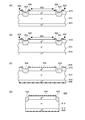
- the step of forming the groove 920 exceeding the pn junction from one surface of the semiconductor substrate on which the pn junction parallel to the main surface is formed (FIG. 6A and FIG.
- a step of forming a passivation glass layer 924 so as to cover the exposed portion of the pn junction inside the groove 920 (see FIG. 6C). Therefore, according to the conventional method for manufacturing a semiconductor device, a high-breakdown-voltage mesa semiconductor device can be manufactured by forming a passivation glass layer 924 in the groove 920 and then cutting the semiconductor substrate. .
- the second step includes a step of forming the glass layer so as to directly cover the exposed portion of the pn junction inside the groove.
- forming the glass layer so as to cover the pn junction exposed portion “directly” means forming the glass layer so as to cover the pn junction exposed portion “directly without an insulating layer or the like”.
- the first step includes a step of forming the pn junction exposed portion on the surface of the semiconductor substrate
- the second step includes the step on the surface of the semiconductor substrate. It is preferable to include a step of forming the glass layer so as to cover the pn junction exposed portion.
- the second step includes a step of forming the glass layer so as to directly cover the pn junction exposed portion on the surface of the semiconductor substrate.
- forming the glass layer so as to cover the pn junction exposed portion “directly” means forming the glass layer so as to cover the pn junction exposed portion “directly without an insulating layer or the like”.
- Pb is not substantially contained because the purpose of the present invention is to use a conventional “glass material containing lead silicate as a main component using a glass material not containing lead”. Similarly, it is possible to manufacture a semiconductor device having a high breakdown voltage.
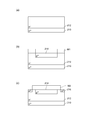
- FIG. 6 is a view for explaining the method for manufacturing the semiconductor device according to the second embodiment.
- FIG. 6 is a view for explaining the method for manufacturing the semiconductor device according to the second embodiment.
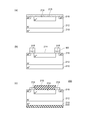
- FIG. 6 is a view for explaining the method for manufacturing the semiconductor device according to the third embodiment.
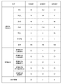
- FIG. 6 is a view for explaining the method for manufacturing the semiconductor device according to the third embodiment. It is a graph which shows the result of an Example. It is a figure shown in order to demonstrate the manufacturing method of the conventional semiconductor device. It is a figure shown in order to demonstrate the manufacturing method of the conventional semiconductor device.
- the glass layer is formed in the second step so as to directly cover the exposed pn junction on the surface of the semiconductor substrate, but the present invention is not limited to this.
- an insulating film may be formed on the exposed pn junction on the surface of the semiconductor substrate, and then a glass layer may be formed so as to cover the exposed pn junction via the insulating film.
Landscapes
- Chemical & Material Sciences (AREA)
- Life Sciences & Earth Sciences (AREA)
- Engineering & Computer Science (AREA)
- Chemical Kinetics & Catalysis (AREA)
- General Chemical & Material Sciences (AREA)
- Geochemistry & Mineralogy (AREA)
- Materials Engineering (AREA)
- Organic Chemistry (AREA)
- Formation Of Insulating Films (AREA)
- Glass Compositions (AREA)
Abstract
L'invention concerne une composition de verre pour la protection de jonctions de semi-conducteurs. Cette composition est caractérisée en ce qu'elle contient au moins SiO2, Al2O3 et ZnO mais qu'elle ne contient sensiblement pas Pb, B, P, As, Sb, Li, Na et K. Il est préférable que la teneur en SiO2 se situe dans la plage de 40-60 % en moles, que la teneur en Al2O3 se situe dans la plage de 5-15 % en moles, et que la teneur en ZnO se situe dans la plage de 30-50 % en moles. Cette composition de verre pour la protection de jonctions de semi-conducteurs permet la production d'un dispositif à semi-conducteur ayant une tension de résistance élevée avec l'emploi d'un matériau de verre exempt de plomb, ladite tension de résistance étant similaire à celles dans les cas où « un verre qui est principalement composé de silicate de plomb » classique est utilisé.
Priority Applications (6)
| Application Number | Priority Date | Filing Date | Title |
|---|---|---|---|
| JP2012511481A JP5139596B2 (ja) | 2011-05-23 | 2011-05-23 | 半導体接合保護用ガラス組成物、半導体装置の製造方法及び半導体装置 |
| PCT/JP2011/061714 WO2012160632A1 (fr) | 2011-05-23 | 2011-05-23 | Composition de verre pour la protection de jonctions de semi-conducteurs, procédé de fabrication d'un dispositif à semi-conducteur et dispositif à semi-conducteur |
| JP2013516273A JP5655139B2 (ja) | 2011-05-23 | 2012-05-08 | 半導体装置の製造方法及び半導体装置 |
| JP2013516274A JP5655140B2 (ja) | 2011-05-23 | 2012-05-08 | 半導体装置の製造方法及び半導体装置 |
| PCT/JP2012/061780 WO2012160962A1 (fr) | 2011-05-23 | 2012-05-08 | Procédé de production de dispositif à semi-conducteurs, et dispositif à semi-conducteurs |
| PCT/JP2012/061779 WO2012160961A1 (fr) | 2011-05-23 | 2012-05-08 | Procédé de production de dispositif à semi-conducteurs, et dispositif à semi-conducteurs |
Applications Claiming Priority (1)
| Application Number | Priority Date | Filing Date | Title |
|---|---|---|---|
| PCT/JP2011/061714 WO2012160632A1 (fr) | 2011-05-23 | 2011-05-23 | Composition de verre pour la protection de jonctions de semi-conducteurs, procédé de fabrication d'un dispositif à semi-conducteur et dispositif à semi-conducteur |
Publications (1)
| Publication Number | Publication Date |
|---|---|
| WO2012160632A1 true WO2012160632A1 (fr) | 2012-11-29 |
Family
ID=47216736
Family Applications (1)
| Application Number | Title | Priority Date | Filing Date |
|---|---|---|---|
| PCT/JP2011/061714 Ceased WO2012160632A1 (fr) | 2011-05-23 | 2011-05-23 | Composition de verre pour la protection de jonctions de semi-conducteurs, procédé de fabrication d'un dispositif à semi-conducteur et dispositif à semi-conducteur |
Country Status (2)
| Country | Link |
|---|---|
| JP (1) | JP5139596B2 (fr) |
| WO (1) | WO2012160632A1 (fr) |
Cited By (2)
| Publication number | Priority date | Publication date | Assignee | Title |
|---|---|---|---|---|
| CN104254907A (zh) * | 2013-03-29 | 2014-12-31 | 新电元工业株式会社 | 半导体接合保护用玻璃复合物、半导体装置的制造方法以及半导体装置 |
| CN116313784A (zh) * | 2021-12-21 | 2023-06-23 | 比亚迪半导体股份有限公司 | 二极管加工方法及二极管 |
Families Citing this family (1)
| Publication number | Priority date | Publication date | Assignee | Title |
|---|---|---|---|---|
| CN104347731A (zh) * | 2013-08-08 | 2015-02-11 | 无锡华润华晶微电子有限公司 | 一种二极管结构 |
Citations (4)
| Publication number | Priority date | Publication date | Assignee | Title |
|---|---|---|---|---|
| JPS556806A (en) * | 1978-06-29 | 1980-01-18 | Toshiba Corp | Semiconductor device |
| JPS5526656A (en) * | 1978-08-17 | 1980-02-26 | Hitachi Ltd | Semiconductor element coverd with glass |
| JP2004115368A (ja) * | 2003-10-31 | 2004-04-15 | Nitto Boseki Co Ltd | ガラス繊維の製造方法、ガラス繊維、ガラス繊維編組物、ガラス繊維強化樹脂及びプリント配線板 |
| JP2009203154A (ja) * | 2008-01-31 | 2009-09-10 | Ohara Inc | ガラス |
Family Cites Families (5)
| Publication number | Priority date | Publication date | Assignee | Title |
|---|---|---|---|---|
| JPS59194441A (ja) * | 1983-04-20 | 1984-11-05 | Toshiba Corp | プレ−ナ型半導体装置 |
| US4714687A (en) * | 1986-10-27 | 1987-12-22 | Corning Glass Works | Glass-ceramics suitable for dielectric substrates |
| JP3943341B2 (ja) * | 2001-02-23 | 2007-07-11 | 日本電気硝子株式会社 | ガラスセラミックス組成物 |
| US7740899B2 (en) * | 2002-05-15 | 2010-06-22 | Ferro Corporation | Electronic device having lead and cadmium free electronic overglaze applied thereto |
| JP4022113B2 (ja) * | 2002-08-28 | 2007-12-12 | 新電元工業株式会社 | 半導体装置の製造方法及び半導体装置 |
-
2011
- 2011-05-23 JP JP2012511481A patent/JP5139596B2/ja active Active
- 2011-05-23 WO PCT/JP2011/061714 patent/WO2012160632A1/fr not_active Ceased
Patent Citations (4)
| Publication number | Priority date | Publication date | Assignee | Title |
|---|---|---|---|---|
| JPS556806A (en) * | 1978-06-29 | 1980-01-18 | Toshiba Corp | Semiconductor device |
| JPS5526656A (en) * | 1978-08-17 | 1980-02-26 | Hitachi Ltd | Semiconductor element coverd with glass |
| JP2004115368A (ja) * | 2003-10-31 | 2004-04-15 | Nitto Boseki Co Ltd | ガラス繊維の製造方法、ガラス繊維、ガラス繊維編組物、ガラス繊維強化樹脂及びプリント配線板 |
| JP2009203154A (ja) * | 2008-01-31 | 2009-09-10 | Ohara Inc | ガラス |
Cited By (3)
| Publication number | Priority date | Publication date | Assignee | Title |
|---|---|---|---|---|
| CN104254907A (zh) * | 2013-03-29 | 2014-12-31 | 新电元工业株式会社 | 半导体接合保护用玻璃复合物、半导体装置的制造方法以及半导体装置 |
| CN104254907B (zh) * | 2013-03-29 | 2016-07-06 | 新电元工业株式会社 | 半导体接合保护用玻璃复合物、半导体装置的制造方法以及半导体装置 |
| CN116313784A (zh) * | 2021-12-21 | 2023-06-23 | 比亚迪半导体股份有限公司 | 二极管加工方法及二极管 |
Also Published As
| Publication number | Publication date |
|---|---|
| JP5139596B2 (ja) | 2013-02-06 |
| JPWO2012160632A1 (ja) | 2014-07-31 |
Similar Documents
| Publication | Publication Date | Title |
|---|---|---|
| JP4927237B1 (ja) | 半導体接合保護用ガラス組成物、半導体装置の製造方法及び半導体装置 | |
| JP5548276B2 (ja) | 半導体接合保護用ガラス組成物、半導体装置の製造方法及び半導体装置 | |
| JP5827398B2 (ja) | 半導体接合保護用ガラス組成物の製造方法、半導体装置の製造方法及び半導体装置 | |
| JP5340511B1 (ja) | 半導体装置の製造方法及び半導体装置 | |
| JP5184717B1 (ja) | 半導体接合保護用ガラス組成物、半導体装置の製造方法及び半導体装置 | |
| JP5508547B1 (ja) | 半導体接合保護用ガラス組成物、半導体装置の製造方法及び半導体装置 | |
| JP5833112B2 (ja) | ガラス組成物の製造方法 | |
| JP5139596B2 (ja) | 半導体接合保護用ガラス組成物、半導体装置の製造方法及び半導体装置 | |
| WO2012160962A1 (fr) | Procédé de production de dispositif à semi-conducteurs, et dispositif à semi-conducteurs | |
| JP4993399B1 (ja) | 半導体接合保護用ガラス組成物、半導体装置の製造方法及び半導体装置 | |
| JP5848821B2 (ja) | 半導体接合保護用ガラス組成物、半導体装置の製造方法、半導体装置及び半導体接合保護用ガラス組成物の製造方法 | |
| JP5655140B2 (ja) | 半導体装置の製造方法及び半導体装置 | |
| JP5655139B2 (ja) | 半導体装置の製造方法及び半導体装置 |
Legal Events
| Date | Code | Title | Description |
|---|---|---|---|
| ENP | Entry into the national phase |
Ref document number: 2012511481 Country of ref document: JP Kind code of ref document: A |
|
| 121 | Ep: the epo has been informed by wipo that ep was designated in this application |
Ref document number: 11866167 Country of ref document: EP Kind code of ref document: A1 |
|
| NENP | Non-entry into the national phase |
Ref country code: DE |
|
| 122 | Ep: pct application non-entry in european phase |
Ref document number: 11866167 Country of ref document: EP Kind code of ref document: A1 |