WO2012161020A1 - Substrat de câblage et panneau d'affichage le comprenant - Google Patents
Substrat de câblage et panneau d'affichage le comprenant Download PDFInfo
- Publication number
- WO2012161020A1 WO2012161020A1 PCT/JP2012/062315 JP2012062315W WO2012161020A1 WO 2012161020 A1 WO2012161020 A1 WO 2012161020A1 JP 2012062315 W JP2012062315 W JP 2012062315W WO 2012161020 A1 WO2012161020 A1 WO 2012161020A1
- Authority
- WO
- WIPO (PCT)
- Prior art keywords
- moth
- substrate
- display panel
- eye structure
- layer
- Prior art date
- Legal status (The legal status is an assumption and is not a legal conclusion. Google has not performed a legal analysis and makes no representation as to the accuracy of the status listed.)
- Ceased
Links
Images

Classifications
-
- H—ELECTRICITY
- H05—ELECTRIC TECHNIQUES NOT OTHERWISE PROVIDED FOR
- H05K—PRINTED CIRCUITS; CASINGS OR CONSTRUCTIONAL DETAILS OF ELECTRIC APPARATUS; MANUFACTURE OF ASSEMBLAGES OF ELECTRICAL COMPONENTS
- H05K1/00—Printed circuits
- H05K1/02—Details
- H05K1/0274—Optical details, e.g. printed circuits comprising integral optical means
-
- G—PHYSICS
- G02—OPTICS
- G02B—OPTICAL ELEMENTS, SYSTEMS OR APPARATUS
- G02B1/00—Optical elements characterised by the material of which they are made; Optical coatings for optical elements
- G02B1/10—Optical coatings produced by application to, or surface treatment of, optical elements
- G02B1/11—Anti-reflection coatings
- G02B1/118—Anti-reflection coatings having sub-optical wavelength surface structures designed to provide an enhanced transmittance, e.g. moth-eye structures
-
- G—PHYSICS
- G02—OPTICS
- G02F—OPTICAL DEVICES OR ARRANGEMENTS FOR THE CONTROL OF LIGHT BY MODIFICATION OF THE OPTICAL PROPERTIES OF THE MEDIA OF THE ELEMENTS INVOLVED THEREIN; NON-LINEAR OPTICS; FREQUENCY-CHANGING OF LIGHT; OPTICAL LOGIC ELEMENTS; OPTICAL ANALOGUE/DIGITAL CONVERTERS
- G02F1/00—Devices or arrangements for the control of the intensity, colour, phase, polarisation or direction of light arriving from an independent light source, e.g. switching, gating or modulating; Non-linear optics
- G02F1/01—Devices or arrangements for the control of the intensity, colour, phase, polarisation or direction of light arriving from an independent light source, e.g. switching, gating or modulating; Non-linear optics for the control of the intensity, phase, polarisation or colour
- G02F1/13—Devices or arrangements for the control of the intensity, colour, phase, polarisation or direction of light arriving from an independent light source, e.g. switching, gating or modulating; Non-linear optics for the control of the intensity, phase, polarisation or colour based on liquid crystals, e.g. single liquid crystal display cells
- G02F1/133—Constructional arrangements; Operation of liquid crystal cells; Circuit arrangements
- G02F1/136—Liquid crystal cells structurally associated with a semi-conducting layer or substrate, e.g. cells forming part of an integrated circuit
- G02F1/1362—Active matrix addressed cells
- G02F1/136286—Wiring, e.g. gate line, drain line
-
- G—PHYSICS
- G02—OPTICS
- G02F—OPTICAL DEVICES OR ARRANGEMENTS FOR THE CONTROL OF LIGHT BY MODIFICATION OF THE OPTICAL PROPERTIES OF THE MEDIA OF THE ELEMENTS INVOLVED THEREIN; NON-LINEAR OPTICS; FREQUENCY-CHANGING OF LIGHT; OPTICAL LOGIC ELEMENTS; OPTICAL ANALOGUE/DIGITAL CONVERTERS
- G02F1/00—Devices or arrangements for the control of the intensity, colour, phase, polarisation or direction of light arriving from an independent light source, e.g. switching, gating or modulating; Non-linear optics
- G02F1/01—Devices or arrangements for the control of the intensity, colour, phase, polarisation or direction of light arriving from an independent light source, e.g. switching, gating or modulating; Non-linear optics for the control of the intensity, phase, polarisation or colour
- G02F1/13—Devices or arrangements for the control of the intensity, colour, phase, polarisation or direction of light arriving from an independent light source, e.g. switching, gating or modulating; Non-linear optics for the control of the intensity, phase, polarisation or colour based on liquid crystals, e.g. single liquid crystal display cells
- G02F1/133—Constructional arrangements; Operation of liquid crystal cells; Circuit arrangements
- G02F1/136—Liquid crystal cells structurally associated with a semi-conducting layer or substrate, e.g. cells forming part of an integrated circuit
- G02F1/1362—Active matrix addressed cells
- G02F1/136286—Wiring, e.g. gate line, drain line
- G02F1/136295—Materials; Compositions; Manufacture processes
-
- G—PHYSICS
- G02—OPTICS
- G02F—OPTICAL DEVICES OR ARRANGEMENTS FOR THE CONTROL OF LIGHT BY MODIFICATION OF THE OPTICAL PROPERTIES OF THE MEDIA OF THE ELEMENTS INVOLVED THEREIN; NON-LINEAR OPTICS; FREQUENCY-CHANGING OF LIGHT; OPTICAL LOGIC ELEMENTS; OPTICAL ANALOGUE/DIGITAL CONVERTERS
- G02F2201/00—Constructional arrangements not provided for in groups G02F1/00 - G02F7/00
- G02F2201/38—Anti-reflection arrangements
Definitions
- the present invention relates to a wiring board and a display panel including the wiring board.
- a display panel such as a liquid crystal display panel
- reflection of external light on the surface is a problem. If the reflectance of the external light on the surface is large, the observer himself, an object placed in the surroundings, a lighting fixture, etc. are reflected and the display is difficult to see. Especially in a bright environment, the reflection is noticeable. Therefore, a low reflection structure is provided on the surface of the display panel to suppress reflection of external light.
- An antireflection technique using a so-called moth-eye structure has been proposed as a low reflection structure that suppresses reflection on the surface of a display panel (see Patent Documents 1 and 2).
- an antireflection film having a moth-eye structure By providing an antireflection film having a moth-eye structure on the surface of the display panel, the reflectance of external light on the surface of the display panel is reduced to about 1% or less.
- reflection on the surface of the display panel is reduced, reflection may occur due to the light reflected inside the display panel, or the contrast ratio of the display may be reduced. Therefore, it is desirable to reduce the reflectivity inside the display panel independently of the reduction in reflection on the surface of the display panel, preferably along with the reduction in reflection on the surface of the display panel.
- the internal reflection of the display panel will be described using a liquid crystal display panel as an example.
- the liquid crystal display panel includes a pair of substrates and a liquid crystal layer provided therebetween.
- One of the pair of substrates has, for example, pixel electrodes, TFTs, and bus lines arranged in a matrix (hereinafter referred to as a TFT substrate).
- the other substrate has a counter electrode, a color filter, and a light shielding layer (black matrix) (hereinafter referred to as a counter substrate).
- the counter substrate is disposed on the viewer side of the liquid crystal layer.
- a liquid crystal display panel in which the counter substrate is disposed on the viewer side of the liquid crystal layer will be described as an example.
- Patent Document 3 a substrate provided with a light-shielding layer having a low reflectance, which is preferably used as a color filter substrate of a liquid crystal display panel.
- This substrate includes a light shielding layer having a high optical density layer and a low optical density layer.
- the present invention has been made to solve the above problems, and an object thereof is to provide a wiring board in which reflection of external light is suppressed and a display panel having such a wiring board. Another object of the present invention is to provide a method for forming a metal layer having an antireflection surface.
- a wiring board includes a substrate and a plurality of metal wirings formed on the substrate, and at least a part of the plurality of metal wirings has a moth-eye structure or an inverted moth-eye structure on the surface.
- a display panel includes a wiring substrate, a counter substrate disposed on the viewer side of the wiring substrate, and a display medium layer provided between the wiring substrate and the counter substrate.
- the wiring board includes a substrate and a plurality of metal wirings provided on the counter substrate side of the substrate, and at least a part of the plurality of metal wirings has a moth-eye structure or an inverted surface. It has a moth-eye structure.
- the counter substrate has a light shielding layer, and the light shielding layer is disposed so as not to overlap the at least part of the plurality of metal wirings.
- the method for forming a metal layer having an antireflection surface includes a step of preparing a mold having a moth-eye structure or an inverted moth-eye structure on the surface, and a step of depositing a metal layer on the surface of the mold And a step of attaching a base material on the metal layer, and a step of peeling the metal layer from the surface of the mold.
- a wiring board in which reflection of external light is suppressed and a display panel having such a wiring board are provided.
- a method for forming a metal layer having an antireflection surface is provided.
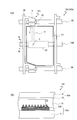
- (A) is a schematic plan view of the liquid crystal display panel 100 of the embodiment according to the present invention
- (b) is a schematic cross-sectional view of the liquid crystal display panel 100
- 1B-1B in (a) It is sectional drawing along a line.
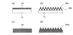
- (A)-(d) is a figure which shows the typical structure of the sample used for the measurement of a reflectance.
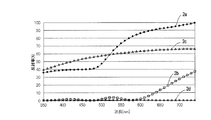
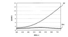
- 3 is a graph showing the spectral reflectance of the sample shown in FIGS. 2 (a) to 2 (d). It is a graph which shows the spectral reflectance of the nickel surface which has a moth-eye structure, and the spectral reflectance of the nickel surface which has an inverted moth-eye structure.
- (A) is a graph of the spectral reflectance of an aluminum layer having an inverted moth-eye structure
- (b) is a diagram showing a schematic structure of a sample used for measurement.
- (A) is a graph which shows the spectral reflectance of the aluminum layer which has a flat surface, and the spectral reflectance of the aluminum layer which has the inverted moth-eye structure
- (b) is typical of the sample used for the measurement. It is a figure which shows a structure.
- (A)-(d) is a schematic diagram for demonstrating the method of forming the metal layer which has a moth-eye type antireflection structure. It is a figure which shows the optical image of the conventional liquid crystal display panel, and has shown two color display pixels.
- a TFT substrate of a liquid crystal display panel is exemplified as the wiring substrate, but the present invention is not limited to the illustrated embodiment, and is applied to various display panels and the wiring substrate.
- FIG. 1A shows a schematic plan view of a liquid crystal display panel 100 according to an embodiment of the present invention
- FIG. 1B shows a schematic cross-sectional view of the liquid crystal display panel 100.
- FIG. 1B is a cross-sectional view taken along line 1B-1B ′ in FIG.
- FIG. 1A shows a planar structure of a region corresponding to one pixel of the TFT substrate 100a included in the liquid crystal display panel 100.
- the TFT substrate 100a includes a substrate (for example, a glass substrate) 11, a TFT formed on the substrate 11, a pixel electrode PE, a source bus line SB, a gate bus line GB, and a CS bus line (auxiliary capacitance wiring) CSB. And have.
- the source electrode S of the TFT is connected to the source bus line SB, and the drain electrode D is connected to the pixel electrode PE.
- the semiconductor layer SC is formed on the gate bus line GB, and the gate electrode of the TFT also serves as the gate bus line GB.
- the liquid crystal display panel 100 includes a TFT substrate 100a, a counter substrate 100b disposed on the viewer side of the TFT substrate 100a, and a liquid crystal layer 32 as a display medium layer provided between the TFT substrate 100a and the counter substrate 100b.
- the counter substrate 100b includes a substrate (for example, a glass substrate) 21 and a counter electrode CE formed on the liquid crystal layer 32 side of the substrate 21.
- the pixel electrode PE and the counter electrode CE of the TFT substrate 100a are provided between them.
- the liquid crystal layer 32 constitutes a pixel.
- the drain extension wiring DE is formed integrally with the drain electrode D.
- An end of the drain extension wiring DE overlaps with the CS bus line CSB via an insulating layer (for example, a gate insulating layer) (not shown), thereby forming an auxiliary capacitor CS. Further, in the contact hole C on the auxiliary capacitor CS, the drain extension wiring DE and the pixel electrode PE are connected.
- the gate bus line GB, the source bus line SB, the drain extension wiring DE, and the CS bus line CSB are metal wirings.
- the drain extension wiring DE, the auxiliary capacitor CS, and the CS bus line CSB can be omitted. Since the structure of the liquid crystal display panel 100 including the TFT substrate 100a is well known, detailed description thereof is omitted.
- the TFT substrate 100a and the liquid crystal display panel 100 can be variously modified.
- the TFT substrate 100a has a moth-eye structure or a moth-eye structure in which at least a part of the metal wiring is inverted on the surface (these are collectively referred to as a moth-eye type antireflection structure 12M).
- FIG. 1B shows an example in which a part of the CS bus line CSB has the moth-eye type antireflection structure 12M on the surface, but the gate bus line GB, the source bus line SB, and the drain extension wiring DE. Any or all of these may have a moth-eye type antireflection structure 12M on the surface.
- an antireflection film having a moth-eye structure can be formed using a porous alumina layer as a mold.
- a porous alumina layer is used, high production efficiency can be obtained.
- a mold in which a porous alumina layer is formed on the outer peripheral surface of a roll is used, there is an advantage that an antireflection film can be continuously formed by a roll-to-roll method.
- the cross-sectional shape of the fine recesses (pores) of the porous alumina layer used in the production of the antireflection film having a moth-eye structure is preferably generally conical or bell-shaped, and the fine recesses have stepped side surfaces. May be.
- the two-dimensional size (opening diameter: D p ) of the fine recess is 10 nm or more and less than 500 nm
- the depth (D depth ) is 10 nm or more and 3000 nm (3 ⁇ m). It is preferable to be less than about.
- the bottom part of a fine recessed part is sharp (the bottom is a point).
- the fine recesses are closely packed, and assuming that the shape of the fine recesses when viewed from the normal direction of the porous alumina layer is a circle, the adjacent circles overlap each other, and the adjacent fine It is preferable that a flange is formed between the recesses.
- the substantially conical minute recesses are adjacent so as to form a collar portion, the two-dimensional size D p of the minute recess is assumed to be equal to the average adjacent distance D int .
- the moth-eye type antireflection structure 12M on the surface of at least a part of the CS bus line CSB of the TFT substrate 100a of the embodiment according to the present invention is preferably a moth-eye structure, as described later, it has an inverted moth-eye structure.
- the moth-eye structure may be represented by Mm
- the inverted moth-eye structure may be represented by Mf.
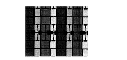
- FIG. 11 is a diagram showing an optical image of a 52-inch liquid crystal display panel marketed by the present applicant, and shows two color display pixels.
- One color display pixel includes four pixels (primary color pixels).
- the primary color pixels are arranged in stripes.
- the portion that appears black in FIG. 11 is a portion formed of a light shielding material, and includes a metal wiring or metal electrode on the TFT substrate and a light shielding layer (black matrix) formed on the counter substrate 100b.
- the light shielding layer is formed so as to overlap with a boundary region of the pixel and a part of the metal wiring.
- the portion of the light shielding layer formed so as to overlap the metal wiring is wider than the metal wiring.
- the pixel aperture ratio (the ratio of the area of the portion that transmits light contributing to display) is reduced.
- the metal wiring of the liquid crystal display panel shown in FIG. 11 is a copper (Cu) wiring.
- the TFT substrate 100a of the embodiment of the present invention has the moth-eye type antireflection structure 12M on the surface of the metal wiring, it is not necessary to form a light shielding layer (black matrix) overlapping at least a portion where the antireflection structure 12M is formed. . Therefore, when the TFT substrate 100a of this embodiment is used, internal reflection of the liquid crystal display panel 100 can be suppressed and the pixel aperture ratio can be increased.
- the antireflection structure 12M may be provided only on the surface of the source bus line SB, and only the light shielding layer provided in the region facing the source bus line SB may be omitted.
- the area of the light shielding layer (the light shielding layer disposed between the pixels and extending in the vertical direction) provided in the region facing the source bus line SB is relatively large. The effect of increasing the pixel aperture ratio by omitting this light shielding layer is relatively large.
- the light shielding layer is formed using a black photosensitive resin layer in a process of forming a color filter layer using a colored photosensitive resin layer, for example.
- the light shielding layer may be formed of a metal layer.
- the light shielding layer may be formed using the technique described in Patent Document 3. For reference, the entire disclosure of Patent Document 3 is incorporated herein.
- FIGS. 2A to 2D show schematic structures of samples used for measuring the reflectance.
- a gold (Au) layer 3Fa (thickness: 50 nm) having a flat surface is formed on a glass substrate 1G.
- the sample shown in FIG. 2B has an inverted moth-eye structure 2Mfa made of a porous alumina layer on a glass substrate 1G, and a gold (Au) layer 3Mfa (thickness: 50 nm) on the inverted moth-eye structure 2Mfa.
- the gold layer 3Mfa has an inverted moth-eye structure.
- the sample shown in FIG. 2C is a nickel (Ni) flat plate 3Fb having a flat surface.
- a surface 3Mma having a moth-eye structure is formed on a nickel substrate 3Fb.
- the nickel surface 3Mma having a moth-eye structure can be formed by electroforming using a porous alumina layer mold (see, for example, Patent Document 2).
- FIG. 3 is a graph showing the spectral reflectance of the samples shown in FIGS. 2A to 2D, and shows the front reflectance measured using a spectrocolorimeter (CM-2600d manufactured by Konica Minolta). ing. Curves 2a to 2d in FIG. 3 show the spectral reflectances of the samples shown in FIGS. 2 (a) to (d), respectively.
- CM-2600d manufactured by Konica Minolta
- the reflectance from the flat metal surface is high, but the moth-eye type antireflection structure is formed on the surface.
- the reflectance can be greatly reduced.
- a curve 2dm in FIG. 4 shows the spectral reflectance of the nickel surface having the moth-eye structure (same as the nickel surface 3Mma in FIG. 2D), and the curve 2df shows the spectral reflection of the nickel surface having the inverted moth-eye structure. Indicates the rate.
- the nickel surface having an inverted moth-eye structure was produced by electroforming using an antireflection film having a moth-eye structure.
- the nickel surface having a moth-eye structure (curve 2dm) is superior in the antireflection effect.
- the nickel surface having the inverted moth-eye structure (curve 2df) has an antireflection effect as compared with the flat nickel surface (curve 2c). You can see that When the flat nickel surface is visually observed, it has a metallic luster similar to copper, but the nickel surface having an inverted moth-eye structure looks black and has no metallic luster.
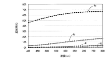
- the dependence of the spectral reflectance of the nickel surface having a moth-eye structure on the height of the convex portion (corresponding to the depth D depth of the concave portion of the moth-eye mold) will be described with reference to FIG.
- the reflectance of the flat nickel surface is shown by a curve 4a for reference.
- Curve 4b is 300 nm in height
- curve 4c is 900 nm in height
- curve 4d shows simulation results for a moth-eye structure having a convex portion with a height of 3000 nm.
- the refractive index (effective refractive index) of the moth-eye structure is equivalent to the refractive index of a laminate having a plurality of layers whose refractive index increases from the air side toward the substrate side (for example, a nickel substrate). it can. That is, the refractive index of the moth-eye structure increases stepwise from the air side to the substrate side. In the illustrated calculation, the number of layers is 30 and the thickness of each layer is equal. The reflectance was calculated based on the effective refractive index medium theory (for example, Tatsuta Tatsuo, Applied Optics (Baifukan) Chapter 4).
- the antireflection effect can be obtained even if the height of the convex portion constituting the moth-eye structure is 300 nm, but the higher the height of the convex portion, the higher the antireflection effect.
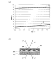
- the sample used for the experiment was obtained by depositing an aluminum layer 3Mfb on a porous alumina layer 2Mfb obtained from the aluminum layer 1A formed on the glass substrate 1G, as shown in FIG. 6 (b).
- the porous alumina layer 2Mfb is illustrated as including a barrier layer.
- curves 6a, 6b, and 6c show the results when the thickness of the aluminum layer 3Mfb is 10 nm, 150 nm, and 50 nm, respectively. If the thickness of the aluminum layer 3Mfb is 10 nm or less, the light transmitted through the aluminum layer 3Mfb is reflected from the underlying aluminum layer 1A, so that the reflectance is increased. On the other hand, when the thickness of the aluminum layer 3Mfb is 150 nm or more, the moth-eye structure is broken by the aluminum deposited between the convex portions of the moth-eye structure, and as a result, the reflectance is increased. Although it depends on the method of forming the metal wiring, the thickness of the metal layer is preferably more than 10 nm and less than 150 nm, and preferably about 50 nm.
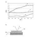
- FIGS. 7A and 7B an aluminum layer having a thickness of about 1 ⁇ m is formed on the antireflection film 2Mm having a moth-eye structure formed on the glass substrate 1G, and the spectral reflectance is measured from both sides.
- the antireflection film 2Mm is obtained by forming an antireflection layer having a moth-eye structure on a TAC film using a photocurable resin.
- the spectral reflectance (incident light L1, reflected light L3) of the upper flat surface 3Fc in FIG. 7B is 80% over the entire measurement wavelength range as shown by the curve 7a in FIG. 7A. Super and very high.
- the spectral reflectance (incident light L1, reflected light L4) of the interface 3Mfc having the inverted moth-eye structure on the lower side in FIG. 7B is the entire measurement wavelength region as shown by the curve 7b. It is 20% or less in the range, and it can be seen that it has an excellent antireflection effect.
- the reflectance shown by the curve 7b includes the reflectance (about 4%) of the surface of the glass substrate 1G, the reflectance from the interface 3Mfc having an inverted moth-eye structure is even lower.
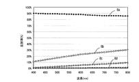
- FIG. 8 shows a simulation result for a moth-eye structure having a convex portion with a height of 300 nm, curve 8c with a height of 900 nm, and curve 8d with a height of 3000 nm.
- the aluminum surface can also have an antireflection effect even when the height of the convex portion constituting the moth-eye structure is 300 nm, but the antireflection effect is higher as the height of the convex portion is higher. Rise.
- FIG. 9 the reflectance of the flat copper surface is shown by a curve 9a for reference.
- a curve 9b shows a simulation result for a moth-eye structure having a convex portion with a height of 300 nm, a curve 9c with a height of 900 nm, and a curve 9d with a height of 3000 nm.
- the copper surface can also have an antireflection effect even when the height of the convex portion constituting the moth-eye structure is 300 nm.
- the higher the height of the convex portion the more the antireflection effect is obtained.
- the height of the convex portion is preferably more than 300 nm, and more preferably 900 nm or more.
- a metal layer having a moth-eye type antireflection structure (a moth-eye structure or an inverted moth-eye structure) on the surface can be formed as follows, for example.
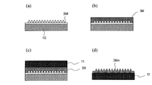
- FIG. 10 is a schematic diagram for explaining a method of forming a metal layer having a moth-eye type antireflection structure.
- a method for forming a metal layer having a moth-eye structure is exemplified, but a metal layer having an inverted moth-eye structure can also be formed by a similar method only by changing the mold.
- a mold having a reversed moth-eye structure (a moth-eye mold) is prepared.
- the moth-eye mold 2Mf formed of a porous alumina layer is formed on the glass substrate 1G by the method described in Patent Document 2.
- the depth D depth of the recess is more than 300 nm.
- a metal layer 3M is deposited on the surface of the moth-eye mold 2Mf.
- the metal layer 3M may be formed in a gas phase, or may be formed in a solution in which a metal is dissolved.
- the substrate 11 is attached to the metal layer 3M using, for example, an adhesive.
- the metal layer 3M having the moth-eye structure on the surface is obtained by peeling the metal layer 3M from the moth-eye mold 2Mf.
- the mold having the inverted moth-eye structure prepared first may be a roll-shaped mold, and the substrate of the mold is not limited to the glass substrate, and substrates of various materials can be used.
- the method of forming the moth-eye structure or the inverted moth-eye structure on the surface of the metal wiring and / or metal electrode of the wiring board has been described, but the present invention is not limited to this, and the formation of the metal layer having the antireflection surface is described. Can be widely applied to the method.
- the metal layer having an antireflection surface can be formed on the surface of a building material, for example. That is, in the above method, by using various base materials in place of the substrate 11, a metal layer having a moth-eye type antireflection surface can be formed on the surfaces of the various base materials.
- the present invention can be widely applied to a wiring board and a display panel including the wiring board.
- the present invention is also used for forming metal layers having various antireflection surfaces.
Landscapes
- Physics & Mathematics (AREA)
- General Physics & Mathematics (AREA)
- Optics & Photonics (AREA)
- Nonlinear Science (AREA)
- Engineering & Computer Science (AREA)
- Microelectronics & Electronic Packaging (AREA)
- Mathematical Physics (AREA)
- Chemical & Material Sciences (AREA)
- Crystallography & Structural Chemistry (AREA)
- Surface Treatment Of Optical Elements (AREA)
- Liquid Crystal (AREA)
- Devices For Indicating Variable Information By Combining Individual Elements (AREA)
Abstract
Un mode de réalisation de la présente invention porte sur un panneau d'affichage (100), qui comprend : un substrat de câblage (100a) ; un substrat de face (100b) qui est positionné sur le côté observateur du substrat de câblage (100a) ; et une couche de milieu d'affichage (32) qui est disposée entre le substrat de câblage (100a) et le substrat de face (100b). Le substrat de câblage (100a) comprend de plus : un substrat (11) ; et une pluralité de fils métalliques (GB, SB, CSB, etc.), qui sont disposés sur le côté de substrat de face (100b) du substrat (11). Au moins une partie de la pluralité de fils métalliques comprennent de plus sur la surface de ceux-ci soit une structure en forme d'œil de mite soit une structure en forme d'œil de mite inversée (12M).
Priority Applications (1)
| Application Number | Priority Date | Filing Date | Title |
|---|---|---|---|
| US14/119,222 US9445494B2 (en) | 2011-05-23 | 2012-05-14 | Wiring substrate and display panel comprising same |
Applications Claiming Priority (2)
| Application Number | Priority Date | Filing Date | Title |
|---|---|---|---|
| JP2011114785 | 2011-05-23 | ||
| JP2011-114785 | 2011-05-23 |
Publications (1)
| Publication Number | Publication Date |
|---|---|
| WO2012161020A1 true WO2012161020A1 (fr) | 2012-11-29 |
Family
ID=47217100
Family Applications (1)
| Application Number | Title | Priority Date | Filing Date |
|---|---|---|---|
| PCT/JP2012/062315 Ceased WO2012161020A1 (fr) | 2011-05-23 | 2012-05-14 | Substrat de câblage et panneau d'affichage le comprenant |
Country Status (2)
| Country | Link |
|---|---|
| US (1) | US9445494B2 (fr) |
| WO (1) | WO2012161020A1 (fr) |
Families Citing this family (1)
| Publication number | Priority date | Publication date | Assignee | Title |
|---|---|---|---|---|
| CN109656099B (zh) * | 2018-11-07 | 2020-07-10 | 深圳市华星光电半导体显示技术有限公司 | 减反阵列基板的制备方法及其制备的减反阵列基板 |
Citations (2)
| Publication number | Priority date | Publication date | Assignee | Title |
|---|---|---|---|---|
| JP2005251488A (ja) * | 2004-03-03 | 2005-09-15 | Hitachi Displays Ltd | 発光素子,発光型表示装置及び照明装置 |
| JP2010205804A (ja) * | 2009-02-27 | 2010-09-16 | Mitsubishi Heavy Ind Ltd | 光電変換装置 |
Family Cites Families (9)
| Publication number | Priority date | Publication date | Assignee | Title |
|---|---|---|---|---|
| US8054416B2 (en) * | 2000-08-15 | 2011-11-08 | Reflexite Corporation | Light polarizer |
| JP4406553B2 (ja) | 2003-11-21 | 2010-01-27 | 財団法人神奈川科学技術アカデミー | 反射防止膜の製造方法 |
| KR100893251B1 (ko) | 2004-12-03 | 2009-04-17 | 샤프 가부시키가이샤 | 반사 방지재, 광학 소자, 및 표시 장치 및 스탬퍼의 제조방법 및 스탬퍼를 이용한 반사 방지재의 제조 방법 |
| JP4703481B2 (ja) * | 2006-05-17 | 2011-06-15 | 東芝モバイルディスプレイ株式会社 | 表示素子 |
| US20080012471A1 (en) * | 2006-06-29 | 2008-01-17 | Eastman Kodak Company | Oled device having improved light output |
| US8687153B2 (en) | 2008-12-19 | 2014-04-01 | Sharp Kabushiki Kaisha | Substrate, and display panel provided with substrate |
| US8405810B2 (en) * | 2009-07-23 | 2013-03-26 | Lg Display Co., Ltd. | Liquid crystal display and fabricating method thereof |
| US8605240B2 (en) * | 2010-05-20 | 2013-12-10 | Semiconductor Energy Laboratory Co., Ltd. | Liquid crystal display device and manufacturing method thereof |
| US8587751B2 (en) * | 2011-02-14 | 2013-11-19 | Samsung Electronics Co., Ltd. | Display panel and display apparatus having the same |
-
2012
- 2012-05-14 WO PCT/JP2012/062315 patent/WO2012161020A1/fr not_active Ceased
- 2012-05-14 US US14/119,222 patent/US9445494B2/en not_active Expired - Fee Related
Patent Citations (2)
| Publication number | Priority date | Publication date | Assignee | Title |
|---|---|---|---|---|
| JP2005251488A (ja) * | 2004-03-03 | 2005-09-15 | Hitachi Displays Ltd | 発光素子,発光型表示装置及び照明装置 |
| JP2010205804A (ja) * | 2009-02-27 | 2010-09-16 | Mitsubishi Heavy Ind Ltd | 光電変換装置 |
Also Published As
| Publication number | Publication date |
|---|---|
| US9445494B2 (en) | 2016-09-13 |
| US20140124243A1 (en) | 2014-05-08 |
Similar Documents
| Publication | Publication Date | Title |
|---|---|---|
| JP3857266B2 (ja) | 反射透過型液晶表示装置とその製造方法 | |
| US10871672B2 (en) | Display panel, production method, and display apparatus | |
| US20180149875A1 (en) | 3D Display Device | |
| WO2018161650A1 (fr) | Panneau d'affichage et dispositif d'affichage | |
| JP6143857B2 (ja) | 双方向視野角の表示パネル及びその製造方法 | |
| TWI464507B (zh) | Active matrix substrate and display device | |
| US10193103B2 (en) | Organic light emitting device having protrusion formed of transparent material and display apparatus | |
| WO2018010428A1 (fr) | Substrat de réseau, substrat d'affichage transparent, dispositif d'affichage transparent et véhicule | |
| US10254581B2 (en) | Fabricating method of color filter substrate, color filter substrate and display device | |
| US8736960B2 (en) | Structure with observation port | |
| US10073274B2 (en) | Grating, manufacturing method thereof and display device | |
| JP2008026654A (ja) | 立体表示装置 | |
| US20150369999A1 (en) | Light guide plate and method of manufacturing the same, and backlight module | |
| TWI507779B (zh) | 液晶顯示器 | |
| JP2017116821A (ja) | 液晶表示装置 | |
| US9235058B2 (en) | Polarization-type three-dimensional display device and manufacturing method thereof | |
| CN102879947A (zh) | 彩色滤光片及其制造方法,半透半反式液晶显示装置 | |
| CN106959481A (zh) | 裸眼立体显示光栅及制造方法、显示装置 | |
| US9810941B2 (en) | Transflective liquid crystal display panel | |
| WO2012161020A1 (fr) | Substrat de câblage et panneau d'affichage le comprenant | |
| CN106648219B (zh) | 触控组件、显示面板及制造触控组件的方法 | |
| CN105700167A (zh) | 3d显示装置 | |
| US20150069426A1 (en) | Display panel | |
| TW201600901A (zh) | 裝飾板以及觸控面板 | |
| JP4703481B2 (ja) | 表示素子 |
Legal Events
| Date | Code | Title | Description |
|---|---|---|---|
| 121 | Ep: the epo has been informed by wipo that ep was designated in this application |
Ref document number: 12789083 Country of ref document: EP Kind code of ref document: A1 |
|
| WWE | Wipo information: entry into national phase |
Ref document number: 14119222 Country of ref document: US |
|
| NENP | Non-entry into the national phase |
Ref country code: DE |
|
| 122 | Ep: pct application non-entry in european phase |
Ref document number: 12789083 Country of ref document: EP Kind code of ref document: A1 |
|
| NENP | Non-entry into the national phase |
Ref country code: JP |