WO2012161065A1 - 薄膜シリカガラスコート量子ドットからなる蛍光性微粒子及びその製造方法 - Google Patents
薄膜シリカガラスコート量子ドットからなる蛍光性微粒子及びその製造方法 Download PDFInfo
- Publication number
- WO2012161065A1 WO2012161065A1 PCT/JP2012/062589 JP2012062589W WO2012161065A1 WO 2012161065 A1 WO2012161065 A1 WO 2012161065A1 JP 2012062589 W JP2012062589 W JP 2012062589W WO 2012161065 A1 WO2012161065 A1 WO 2012161065A1
- Authority
- WO
- WIPO (PCT)
- Prior art keywords
- quantum dots
- fine particles
- fluorescent fine
- silica glass
- fluorescent
- Prior art date
- Legal status (The legal status is an assumption and is not a legal conclusion. Google has not performed a legal analysis and makes no representation as to the accuracy of the status listed.)
- Ceased
Links
Images

Classifications
-
- C—CHEMISTRY; METALLURGY
- C09—DYES; PAINTS; POLISHES; NATURAL RESINS; ADHESIVES; COMPOSITIONS NOT OTHERWISE PROVIDED FOR; APPLICATIONS OF MATERIALS NOT OTHERWISE PROVIDED FOR
- C09K—MATERIALS FOR MISCELLANEOUS APPLICATIONS, NOT PROVIDED FOR ELSEWHERE
- C09K11/00—Luminescent materials, e.g. electroluminescent or chemiluminescent
- C09K11/02—Use of particular materials as binders, particle coatings or suspension media therefor
- C09K11/025—Use of particular materials as binders, particle coatings or suspension media therefor non-luminescent particle coatings or suspension media
-
- B—PERFORMING OPERATIONS; TRANSPORTING
- B82—NANOTECHNOLOGY
- B82Y—SPECIFIC USES OR APPLICATIONS OF NANOSTRUCTURES; MEASUREMENT OR ANALYSIS OF NANOSTRUCTURES; MANUFACTURE OR TREATMENT OF NANOSTRUCTURES
- B82Y20/00—Nanooptics, e.g. quantum optics or photonic crystals
-
- B—PERFORMING OPERATIONS; TRANSPORTING
- B82—NANOTECHNOLOGY
- B82Y—SPECIFIC USES OR APPLICATIONS OF NANOSTRUCTURES; MEASUREMENT OR ANALYSIS OF NANOSTRUCTURES; MANUFACTURE OR TREATMENT OF NANOSTRUCTURES
- B82Y30/00—Nanotechnology for materials or surface science, e.g. nanocomposites
-
- B—PERFORMING OPERATIONS; TRANSPORTING
- B82—NANOTECHNOLOGY
- B82Y—SPECIFIC USES OR APPLICATIONS OF NANOSTRUCTURES; MEASUREMENT OR ANALYSIS OF NANOSTRUCTURES; MANUFACTURE OR TREATMENT OF NANOSTRUCTURES
- B82Y40/00—Manufacture or treatment of nanostructures
-
- C—CHEMISTRY; METALLURGY
- C09—DYES; PAINTS; POLISHES; NATURAL RESINS; ADHESIVES; COMPOSITIONS NOT OTHERWISE PROVIDED FOR; APPLICATIONS OF MATERIALS NOT OTHERWISE PROVIDED FOR
- C09K—MATERIALS FOR MISCELLANEOUS APPLICATIONS, NOT PROVIDED FOR ELSEWHERE
- C09K11/00—Luminescent materials, e.g. electroluminescent or chemiluminescent
- C09K11/08—Luminescent materials, e.g. electroluminescent or chemiluminescent containing inorganic luminescent materials
- C09K11/56—Luminescent materials, e.g. electroluminescent or chemiluminescent containing inorganic luminescent materials containing sulfur
- C09K11/562—Chalcogenides
- C09K11/565—Chalcogenides with zinc cadmium
-
- C—CHEMISTRY; METALLURGY
- C09—DYES; PAINTS; POLISHES; NATURAL RESINS; ADHESIVES; COMPOSITIONS NOT OTHERWISE PROVIDED FOR; APPLICATIONS OF MATERIALS NOT OTHERWISE PROVIDED FOR
- C09K—MATERIALS FOR MISCELLANEOUS APPLICATIONS, NOT PROVIDED FOR ELSEWHERE
- C09K11/00—Luminescent materials, e.g. electroluminescent or chemiluminescent
- C09K11/08—Luminescent materials, e.g. electroluminescent or chemiluminescent containing inorganic luminescent materials
- C09K11/88—Luminescent materials, e.g. electroluminescent or chemiluminescent containing inorganic luminescent materials containing selenium, tellurium or unspecified chalcogen elements
- C09K11/881—Chalcogenides
- C09K11/883—Chalcogenides with zinc or cadmium
Definitions
- the present invention relates to fluorescent fine particles in which quantum dots having high luminous efficiency are covered with silica glass produced by a sol-gel method, and to a production method and application thereof.
- Phosphors in which rare earth ions, transition metal ions, and the like are dispersed in an inorganic material have superior durability compared to organic dyes, and thus have been conventionally used in lighting, displays, and the like.
- luminance and color rendering properties are not always sufficient, there has been a demand for phosphors that surpass them.
- quantum dots about 2 to 10 nm in diameter, sometimes called “semiconductor nanoparticles” or “semiconductor ultrafine particles” have attracted much attention as new high-performance phosphors that have a high possibility of realizing this. .
- the quantum dot emits bright fluorescence having various wavelengths according to the particle diameter even when irradiated with ultraviolet rays having the same wavelength, and thus has excellent color rendering properties, and the luminance can be increased because the emission decay time is short. If the quantum dots are carefully prepared, the brightness is high enough to detect and separate the light emission of each particle separately. Therefore, in addition to the display and illumination, it is combined with biomolecules to make life as a fluorescent reagent.
- the field of application used for elucidation of diseases, diagnosis of diseases, etc. is about to develop greatly.
- Quantum dots serving as such phosphors are mainly composed of II-VI group semiconductors (cadmium sulfide (CdS), zinc selenide (ZnSe), cadmium selenide (CdSe), zinc telluride (ZnTe), cadmium telluride ( CdTe), mixed crystals thereof, and the like) and III-V group semiconductors (such as indium phosphide (InP)). These semiconductors exhibit direct transitions and have an emission lifetime of about 10 nanoseconds, which is about 5 orders of magnitude shorter than phosphors using rare earth or transition metal ions with the characteristics of forbidden transitions. Fluorescence is obtained.
- II-VI group semiconductors cadmium sulfide (CdS), zinc selenide (ZnSe), cadmium selenide (CdSe), zinc telluride (ZnTe), cadmium telluride ( CdTe), mixed crystals thereof, and the like
- III-V group semiconductors such as indium
- quantum dots that emit light with high brightness As for quantum dots that emit light with high brightness in this way, a method of synthesizing them in an aqueous solution (hydrophilic quantum dots are synthesized) and a method of synthesizing them at high temperatures in an organic solution excluding water (hydrophobic) Two quantum dots are synthesized). Since the quantum dot has a large specific surface area, the light emission efficiency is lowered by gradually agglomerating in the solution to reduce the surface energy. For this reason, there is a problem that it is difficult to apply the quantum dots synthesized by either method as they are in solution. In order to solve this, it is necessary to cover the quantum dots with a transparent matrix, and to make the material maintain the initial characteristics over a long period of time in various environments.
- the sol-gel method is advantageous. This is because the sol-gel method allows vitrification to proceed under mild conditions around room temperature and normal pressure, so if the fabrication method is devised, the quantum dots retain high luminous efficiency immediately after being synthesized by the solution method. This is because they are dispersed and fixed in transparent glass.
- Silica glass is strong because it has a solid three-dimensional network structure compared to organic polymers made of carbon, and has a low diffusion coefficient of the material, and has excellent properties to protect what is contained in it.
- tetrafunctional silicon alkoxides those in which all R are ethyl groups (Si (OC 2 H 5 ) 4 ) are best known, and are called tetraethyl orthosilicate, tetraethoxysilane, or tetraethoxy orthosilicate. In the present specification, this is abbreviated as TEOS.
- a tetrafunctional silicon alkoxide in which one or two alkoxy groups are substituted with an alkyl group (or a derivative thereof) X is called an organic alkoxysilane or a silane coupling agent, and is represented by the formula (I): X n -Si (OR 1 ) 4-n (I) It is represented by In the above formula (I), X represents a group represented by CH 2 ⁇ CH—, a group containing oxirane, a group represented by H 2 NC m H 2m —, CH 2 ⁇ C (CH 3 ) COOC p H 2p A group represented by —, a group represented by HSC q H 2q —, or a phenyl group (where m is an integer of 1 to 6, p is an integer of 1 to 5, and q is an integer of 1 to 10).
- R 1 is a lower alkyl group, and n is 1 or 2.
- the organoalkoxysilane is a (4-n) functional (n is 1 or 2) alkoxide.
- Organoalkoxysilane is also solidified by sol-gel reaction, and the resulting product is sometimes called glass. However, since there are at most three bonds, the power to suppress the diffusion of the substance is weaker than that of glass made from tetrafunctional silicon alkoxide, and it has the property of an organic polymer. Solid materials made using organoalkoxysilanes are sometimes referred to as organic-inorganic hybrid materials.
- Patent Document 1 bulk glass
- Patent Documents 2 to 4 glass fine particles
- Patent Document 5 glass thin film
- the average of the lengths of the three principal axes of inertia is defined as the particle diameter (in the case of a perfect sphere, the diameter is the particle diameter) is a powdered phosphor for a light emitting device such as a display or illumination.
- the description is limited to the fluorescent silica glass fine particles.
- a sol-gel method in which an alkoxide is hydrolyzed and dehydrated and condensed is used.
- the reverse micelle method a method in which the sol-gel method is advanced in minute polka dots dispersed in an oil phase, water-dispersible quantum dots are dispersed in polka dots in advance
- the Stover method hydrolyzed
- the particle size is about 10 nm for proteins, about 25 nm for ribosomes, about 100 nm for viruses, and about 7 ⁇ m for red blood cells.
- the glass is not made of an organoalkoxysilane, and silica glass made from tetrafunctional silicon alkoxide is most preferable.
- the size of the obtained glass-coated fluorescent fine particles is preferably 15 nm or less and an average glass film thickness of 3 nm or less.
- the quantum dots are directly covered with a glass synthesized from a tetrafunctional silicon alkoxide while maintaining the light emission characteristics as much as possible without using an organoalkoxysilane or a polymer. It is preferable.
- a method for synthesizing such a fluorescent fine particle that is small and has high luminous efficiency has not been known as described in detail below.
- Fluorescent silica glass fine particles in which CdSe / ZnS quantum dots are dispersed and fixed in glass by a sol-gel method and a method for producing the same are reported by Babendi et al. (Non-patent Document 1).
- the surface of a quantum dot previously synthesized in an organic solvent is covered with an alkoxide having an amino group (3-aminopropyltrimethoxysilane) and an alcohol having an amino group (5-amino-1-pentanol).
- a separately prepared silica glass fine particle having a diameter of several hundreds of nanometers is adhered as a layer having a thickness of about 50 nm.
- fluorescent glass fine particles having a structure in which the surface of silica glass fine particles not containing quantum dots is coated with a sol-gel glass layer containing quantum dots can be obtained.
- quantum dots exist only in the vicinity of the surface layer of the glass fine particles, and the quantum dots are not contained in the nuclei of the glass fine particles, so that the dispersion concentration of the quantum dots in the glass fine particles cannot be increased.
- the luminous efficiency was about 13%.
- Non-Patent Document 2 alkoxide having a thiol group (a kind of organic alkoxysilane) is grown on the surface of CdSe / ZnS quantum dots, and silica glass fine particles containing one quantum dot in one silica glass fine particle are grown.
- a production method has been reported (Non-Patent Document 2).
- the luminous efficiency in this case is reported to be 5-18%.
- silica glass fine particles having a particle diameter of 30 nm to 1 ⁇ m containing one CdSe / ZnS quantum dot produced by a similar method have been reported, but the luminous efficiency is not described (Non-patent Document 3).
- the light emission efficiency rapidly decreases immediately after the production, further gradually decreases, and after 1 week, 2% of the state before entering the silica glass ( The absolute value is from the initial 60% to 1.2%).
- a quantum dot having a particularly thick shell is used, the luminous efficiency is increased.
- such a quantum dot having a particularly thick shell has a large particle size and is not suitable for biotechnology applications, and it is difficult to produce such a quantum dot.
- Non-patent Document 5 There is also known a study in which water-dispersible CdSe quantum dots (citric acid coat) are prepared and introduced into a plurality of silica glass particles.
- water-dispersible CdSe quantum dots have an extremely low luminous efficiency of 0.1 to 0.15%. Although there is no description about the light emission efficiency when the quantum dots are introduced into the silica matrix, the light emission efficiency is usually further reduced, so this cannot be called a phosphor.
- Non-patent Literature 6 in which water-dispersible CdSe quantum dots are introduced into silica particles by the reverse micelle method, the luminous efficiency is 1.48% at most. I can't call it.
- a rough guide that can be called a phosphor is a luminous efficiency of 20% or more.
- Non-patent Document 7 a method of adding ammonia and TEOS after covering CdSe quantum dots with aminopropyltrimethoxysilane (a kind of organic alkoxysilane) has been reported (Non-patent Document 7). Further, CdSe / ZnS quantum dots are modified with polyethylene glycol and then added with ammonia and TEOS. The luminous efficiency in this case is about 17% at the maximum, and glass beads that do not contain quantum dots are sometimes seen in a transmission electron microscope image.
- Non-patent document 8 The same group has also reported glass beads in which quantum dots and magnetic nanoparticles are dispersed.
- the reverse micelle method is used, but the size (particle size) of the produced glass beads is reported to be about 50 nm, and the luminous efficiency is reported to be 4.8% at the maximum.
- glass beads having a diameter of about 30 nm can be obtained by adding TEOS after dispersing the quantum dots in the oil phase by reverse micelle method, and then adding ammonia after stirring for about 30 minutes (Non-Patent Document). 9). Although there is no report of luminous efficiency here, it is expected that luminous efficiency is not high because the reported fluorescence spectrum has a lot of noise. Our additional experiments also show that this method does not provide high luminous efficiency. This research was continued by the same researcher, but the diameter of the obtained glass beads was about 30 nm, and the luminous efficiency was not reported (Non-patent Document 10).
- Non-patent Document 11 a quantum dot covered only with organic alkoxysilane without using any tetrafunctional silicon alkoxide has been reported (Non-patent Document 11).
- CdSe / ZnS stabilized with a ligand trioctylphosphine oxide, etc.
- three types of organoalkoxysilanes in order to make them hydrophilic, form a shell, and functionalize the surface. .
- the size is increased to 17.4 ⁇ 2.1 nm. Since the particle diameter estimated from the TEM image and the first absorption peak wavelength of the quantum dots is about 3 nm, the thickness of the coat around the quantum dots is 7 nm or more.
- Quantum dots containing Cd and Se are known to be hydrophilic with an aqueous solution and hydrophobic with an organic solution. Hydrophobic ones have higher luminous efficiency, narrower fluorescence spectrum width, and better durability.
- hydrophilic CdTe quantum dots and the like are put in glass beads. In this case, the spectrum width (full width at half maximum) becomes wide to the extent that it exceeds 60 nm in the red region (640 nm). When a ternary system is made by mixing Zn, Se, etc., this spectral width is further expanded.
- the number of quantum dots contained in the glass beads exceeded one, and it was impossible to produce those having an average particle size of 15 nm or less. Furthermore, the quantum dots are distributed throughout the glass beads and do not have a silica glass protective layer. In addition, since a large amount of TEOS was introduced, the viscosity of the solution was increased, and the size distribution of the glass beads to be produced was as wide as several tens of nm to several ⁇ m.
- fluorescent fine particles coated with a silica glass thin film made of an alkoxide having a quantum dot containing Cd and Se having an average film thickness of 3 nm or less and an average particle diameter of 15 nm or less have not been known.
- Non-patent Document 12 a method for producing an assembly of a plurality of quantum dots using a linear polymer has recently been reported (Non-patent Document 12).
- the polymer particles produced by this method have been reported to have an average particle size measured by dynamic light scattering of 112 nm, but it is difficult to produce a quantum dot aggregate having a particle size of 100 nm or less.
- the surface of the aggregate can be further coated with glass, but the particle size further increases.
- a glass material not containing a polymer is more durable and has a smaller amount of Cd elution, so that it is required to produce a glass material without using a polymer.
- the produced material when used for in-vivo imaging (in vivo), it is important to select a wavelength region in which absorption by substances in the organism is small. For this purpose, it is important to emit light in a wavelength range of 650 to 1000 nm called a “biological window” while avoiding the absorption region of hemoglobin, water, etc. (http: //www.aist.go. jp / aist_j / press_release / pr2009 / pr20090908 / pr20090908.html). Quantum dots that emit light in this wavelength range are commercially available. However, with a known production method, quantum dots having a luminous efficiency of 20% or more could not be obtained.
- Japanese Patent No. 4366502 Japanese Patent No. 3767538 Japanese Patent No. 3755033 No. 2007/034877 JP 2006-282777 A Japanese Patent No. 4555966
- the inventors have so far produced silica glass-coated quantum dots of various forms (bulk bodies, thin films, fibers, fine particles) mainly using CdTe quantum dots.
- silica glass-coated quantum dots of various forms (bulk bodies, thin films, fibers, fine particles) mainly using CdTe quantum dots.
- the conditions for evaluating the fluorescence characteristics are usually greatly different from those for the production of other materials.
- Silica glass fine particles have little scattering if the particle size is about 100 nm or less, so that the silica glass fine particles are introduced into a quartz cell having an optical path length of 1 cm while being dispersed in a solution, and they are introduced into general-purpose absorption spectrophotometers and fluorescence spectrophotometers. Measure with Thereby, the absorbance and fluorescence intensity for each wavelength are obtained. An integrating sphere is used when the influence of scattering is a concern. At this time, both the absorbance and the fluorescence intensity have a larger error than when there is no scattering. Also in this case, recently, a general-purpose measuring apparatus is commercially available (for example, C9920-02 of Hamamatsu Photonics Co., Ltd.).
- the concentration of the quantum dots at the time of synthesis is usually about 1 to 10 ⁇ M (micromol / liter, the number of quantum dots, not the number of atoms constituting them), and this is stored in a cool and dark place as it is.
- the concentration is too high, so it is diluted to about 200 to 300 nM. If it does so, the signal amount which is the easiest to measure with a general-purpose absorption spectrophotometer or fluorescence spectrophotometer is obtained.
- the solvent is often pure water.
- the quantum dot concentration is at most about 10 nM, and physiological Dispersed in high concentration salt such as saline.
- the irradiation light intensity is usually 10 W / cm 2 or more, which is much higher than that of the spectroscope.
- the dispersion concentration of quantum dots is extremely low, and even if the solution contains a large amount of salts, even if it is coated on glass, especially in the case of CdTe quantum dots Has been found to deteriorate rapidly. In order to suppress such deterioration, it is necessary to use quantum dots other than CdTe quantum dots.
- the present invention has been made in order to solve the problems described in the background art and the degradation found in glass-coated CdTe quantum dots, and its purpose is to achieve high durability and small fluorescence with high brightness. Providing fine particles. Furthermore, it is also an object of the present invention to show a technique for applying it to the fluorescent reagent in the bio field, the electronic material field and the like.
- Step 1 An appropriate amount of silicon alkoxide (1) is added to a hydrophobic solvent in which quantum dots containing Cd and Se are dispersed and stirred. Since the hydrophobic solvent takes in a very small amount of moisture from the air, only one of the four alkoxy groups is gradually hydrolyzed to (RO) 3 —Si—OH in the silicon alkoxide (1). . It was found that this molecule replaced the ligand coordinated on the surface of the quantum dot at the time of fabrication and directly covered the quantum dot. If the hydrolysis reaction is slow, (RO) 3 —Si—OH neatly arranges and covers the quantum dots, so that a decrease in luminous efficiency can be suppressed.
- Step 2 Next, in this step, a thin silica glass layer is applied to the surface of the surface silanized quantum dots.
- a method of preparing a reverse micelle solution water is dispersed in the form of droplets in the oil phase
- the quantum dots are dispersed in a continuous phase made of a hydrophobic solvent and then distributed to the droplet phase.
- silicon alkoxide (2) is added. Since the silicon alkoxide (2) used in this step is distributed into a hydrophobic continuous phase, it is gradually hydrolyzed by touching water dispersed as droplets. Further, since the silicon alkoxide (1) attached to the surface of the quantum dot is also gradually hydrolyzed, the quantum dot becomes hydrophilic and is converted into an aqueous phase.
- the hydrolyzed silicon alkoxide (2) used in Step 2 gradually moves to the aqueous phase and is deposited on the surface of the quantum dots for dehydration condensation.
- the reaction rate is low, the thickness of the silica glass can be finely controlled.
- a uniform film is formed.
- it since it is in the reverse micelle, it collides with other quantum dots and does not aggregate, and one quantum dot is dispersed in one glass bead. In addition, formation of empty glass beads that do not include quantum dots can be suppressed.
- Step 2 is not limited to the reverse micelle method described above.
- the reverse micelle method is not used, for example, in Step 2, a small amount of silicon alkoxide (1) is added stepwise to prevent the formation of empty glass beads, and the glass on the surface of the quantum dots What is necessary is just to devise, such as performing layer formation gradually and making it easy to control a film thickness.
- the present inventors have described that the quantum dot-dispersed fluorescent silica glass fine particles containing Cd and Se produced by the sol-gel method devised in this way include silica glass made from an alkoxide having an average film thickness of 3 nm or less. It was confirmed that the fluorescent fine particles coated with a thin film were provided and the luminous efficiency was 20% or more. Based on such knowledge, the present inventors have further studied and completed the present invention.
- the present invention provides the following highly durable and high-luminance fine silica glass thin film coated quantum dots (fluorescent fine particles) and a method for producing the same by a sol-gel method. Furthermore, the present invention provides a long-wavelength emission quantum dot that can be used for in vivo imaging and a silica thin film coating method thereof. In in vivo imaging, since quantum dots are inserted into a living body, it is very advantageous to have durability and low elution of cadmium.
- Item 1 Fluorescent fine particles obtained by coating quantum dots containing Cd and Se with a thin film containing silica glass made of silicon alkoxide having an average film thickness of 3 nm or less.
- the fluorescent fine particle according to Item 1 wherein the quantum dot comprises a core containing Cd and Se and a shell containing Zn and S.
- Item 3. Item 3.
- Item 4. Item 4.
- Item 6. Item 6.
- Item 7. The fluorescent fine particles according to any one of Items 1 to 6, wherein the average particle size is 15 nm or less.
- Item 8. The fluorescent fine particles according to any one of Items 1 to 7, which have at least one kind selected from the group consisting of COOH groups, NH 2 groups, SH groups and salts thereof, and groups derived from polyethylene glycol on the surface.
- Item 9. Item 9. The fluorescent fine particle according to any one of Items 1 to 8, wherein the number of quantum dots is one.
- Item 10. Item 10. The fluorescent fine particle according to any one of Items 1 to 9, wherein the luminous efficiency is 20% or more.
- Item 11. Item 11.
- Item 12. Item 11.
- Item 13. Item 11.
- Item 14. (1) The fluorescent fine particle according to any one of Items 1 to 13, comprising a step of preparing a hydrophobic quantum dot by stirring a quantum dot containing Cd and Se and a hydrophobic solvent containing silicon alkoxide for 1 hour or more. Manufacturing method.
- Item 16. Item 16.
- the quantum dots containing Cd and Se are produced in a process including the condition of 0.3X ⁇ Y ⁇ 2X where the amount of Cd contained in the solution is X mmol and the speed of Se to be added is Y mmol / min.
- the fluorescent fine particles of the present invention durable quantum dots are covered with an even thinner silica glass thin film.
- a device for maintaining the original luminous efficiency is also devised. Since the fluorescent fine particles of the present invention have an overall particle size of 15 nm or less, they can be applied to a wide range of fields as fluorescent reagents.
- the quantum dot is covered with silica glass, and then confirms that silicon and oxygen are contained by analysis of the corresponding part with an analytical electron microscope. be able to.
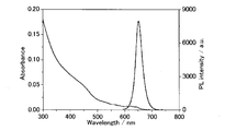
- the left curve and axis are absorption spectra, and the right curve and axis are fluorescence spectra.
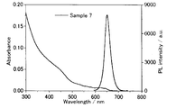
- 6 is an absorption and fluorescence spectrum of the fluorescent fine particles produced in Example 5.
- FIG. The left curve and axis are absorption spectra, and the right curve and axis are fluorescence spectra.
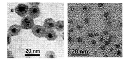
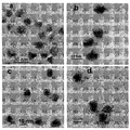
- transmission electron microscope images of Examples 1 and 2 coated with QD1 are shown as a and b, respectively.
- transmission electron microscope images of Examples 3 to 6 coated with QD2 are shown as a to d in order.
- What is produced by the present invention is a phosphor in which one quantum dot containing Cd and Se is coated with a thin film containing silica glass having an average film thickness of 3 nm or less.
- step 1 Production of quantum dots 2. surface silanization (step 1); 3. Silica glass thin film coating and surface modification (Step 2) 4. Evaluation and It demonstrates in order of a use.
- Quantum dots containing Cd and Se which are characterized by high stability and a narrow fluorescence spectrum width and high luminous efficiency, are used. First, a method for producing quantum dots containing Cd and Se will be described.
- the quantum dots used in the present invention are not limited as long as they contain Cd and Se, and are not necessarily composed only of Cd and Se.
- quantum dots doped with rare earth ions, transition metal ions, etc. can obtain fluorescence from rare earth ions and transition metal ions, and it is difficult to obtain the fluorescence characteristics of quantum dots.
- Undoped quantum dots are preferred. Specifically, CdSe, CdSe / ZnS (CdSe quantum dots coated with ZnS), CdSe / CdS / Cd 0.5 Zn 0.5 S / ZnS (CdS, Cd 0.5 Zn 0.5 S and ZnS were sequentially coated with CdSe as the nucleus.
- Quantum dots alloy compositions such as CdSe x Te 1-x (0 ⁇ x ⁇ 1), and the like.
- shells such as ZnS, ZnSe, and CdS, on the surface is excellent.
- This shell may have a gradient composition in which the composition of Cd, Zn, Se, S, etc. changes in the thickness direction of the shell.
- Non-Patent Documents 13 to 22 As the method for producing such quantum dots containing Cd and Se, the following 10 known methods are known (Non-Patent Documents 13 to 22).
- the average particle size of quantum dots produced by these methods is about 2 to 9 nm.
- the ligand in this step has a low binding energy. Is desirable.
- Specific ligands include phosphate compounds with alkyl groups (trioctylphosphine, trioctylphosphine oxide, etc.), alkylamines (hexadecylamine, octadecylamine, oleylamine, myristylamine, laurylamine, etc.), olein An acid etc. are mentioned.
- quantum dots having an emission peak wavelength of 650 to 1000 nm cannot be obtained by these production methods.
- cadmium oxide 0.3 to 0.7 mmol (more preferably 0.5 to 0.6 mmol), octadecylphosphonic acid 150 to 200 mg (more preferably 175 to 185 mg) and 3 to 10 mL (more preferably 4 to 6 mL) of trioctylamine (TOA) in a glass container
- TOA trioctylamine
- 0.5 to 2 mmol (more preferably 0.8 to 1.2 mmol) of selenium powder is dissolved in 1 mL of trioctylphosphine (TOP) to produce TOPSe (with selenium bonded to TOP).
- TOP trioctylphosphine
- TOPSe with selenium bonded to TOP.
- 0.15 to 0.4 mL / min (more preferably 0.2 to 0.3 mL / min) TOPSe is injected at a speed of). After reacting for 4 to 8 minutes (more preferably 5 to 7 minutes), the core is obtained by cooling to near room temperature and further purification.
- the injection speed may be changed in inverse proportion to the concentration of TOPSe in the TOP solution to be injected. Further, it may be changed in proportion to the amount of cadmium previously dispersed in the container. In general, when the amount of Cd contained in the solution is X mmol and the speed of Se injected into this is Y mmol / min, 0.3X ⁇ Y ⁇ 2X And 0.5X ⁇ Y ⁇ 1.5X More preferably. When the emission wavelength is longer than 700 nm, it is advantageous to add Te as TOPTE (a combination of Te and TOP; obtained by dissolving Te powder in TOP) during TOPSe injection. .
- the method for producing the core CdSe is not limited to the above, and the Cd raw material, the Se raw material, the type of the solvent for dissolving Cd or Se, and the like may be appropriately changed as necessary.
- a hexane solution of Cd (CH 3 ) 2 can be used as the Cd raw material.
- the solvent trioctylphosphine oxide (TOPO), hexadecylamine (HDA) or the like can be used, and the reaction temperature in this case is 290 to 295 ° C.
- HDA has two roles: a solvent and a ligand attached to CdSe.
- the reaction temperature is preferably about 300 ° C.
- the core consists of Cd and Se only in order to narrow the fluorescence spectrum width and increase the durability.
- Te or the like is further contained in the core, long wavelength light emission can be obtained.
- the content of other elements such as Te is preferably 30 mol% or less, and more preferably 10 mol% or less, in order to maintain durability and fluorescence spectrum width.
- Quantum dot cores can be made in two ways: when made with an aqueous solution at about 100 ° C. (a hydrophilic core can be made) and when made with a high-temperature organic solution at about 300 ° C. (made a hydrophobic core).
- the organic solution method is preferable for producing quantum dots having high durability and a narrow fluorescence spectrum width.
- the non-patent documents 13 to 22 are also produced by the organic solution method.
- the core produced by the organic solution method has higher luminous efficiency when a shell is attached thereafter.
- the light emission wavelength at the core stage is preferably 618 nm or more, and more preferably 620 nm or more. It is more preferable.
- the average size of the resulting quantum dots is typically 9-11 nm. However, if it is not spherical, the average value of the sizes in the three principal axes of inertia is taken as the size of one particle.
- the shell When the shell is formed, for example, when a shell made of Cd, Zn and S is formed, a salt of Cd and Zn, for example, acetate is added at a Cd to Zn ratio of about 1: 1. Convenient. Cd is preferentially attached to the CdSe core due to the lattice constant, etc., followed by Zn. From the composition at this time, the quantum dot may be written as CdSe / Cd x Zn 1-x S. S may be reacted with Cd or Zn by using TOPS (a powder of S dissolved in TOP) as in the case of Se and Te described above.
- TOPS a powder of S dissolved in TOP
- the shell manufacturing method is not limited to the above, and is appropriately selected as necessary.
- diethyl zinc can be used as a raw material for zinc
- hexamethyldisilathiane common name: thiobis (trimethylsilane)
- Hexamethyldisilathiane Hexamethyldisilathiane (Thiobis (trimethylsilane))
- Thiobis trimethylsilane
- Step 1 A quantum dot containing Cd and Se can be manufactured by the above-described method. However, this quantum dot is hydrophobic because it is produced in an organic solvent excluding water. In order to perform hydrolysis and dehydration condensation using the sol-gel method, it is advantageous that the quantum dots are hydrophilic. Therefore, in this step, the surface of the quantum dots is silanized with silicon alkoxide (1).
- an alkylamine ligand eliminates surface defects and improves luminous efficiency, whereas a ligand composed of a partially hydrolyzed silicon alkoxide (for example, (Et—O) 3 —Si—O ⁇ ) has been reported to have a sharp decrease in luminous efficiency due to its quenching action. On the other hand, it was unclear why hydrolyzed silicon alkoxide has a quenching effect.
- a partially hydrolyzed silicon alkoxide for example, (Et—O) 3 —Si—O ⁇
- Non-Patent Document 13 a primary alkylamine having no branching is useful.
- an aggregate of quantum dots can be formed by surface coating with a silicon alkoxide (1) in a hydrophobic solvent and then contacting with a large amount of water containing another silicon alkoxide (2). .
- the conditions for surface coating of the silicon alkoxide (1) at this time were optimized and surface silanization was performed. Further, as described in the next section (silica glass thin film coating and surface modification), a thin silica glass layer can be formed by gradually reacting with a small amount of water.
- the quantum dots prepared in the previous section are dispersed in a hydrophobic solvent.
- the hydrophobic solvent is not particularly limited, and examples thereof include toluene, chloroform, hexane and the like, and toluene is particularly preferable.
- the quantum dot concentration at this time is preferably 0.1 to 20 ⁇ M (micromol / liter), more preferably 0.5 to 10 ⁇ M, and most preferably 1 to 5 ⁇ M.
- a silicon alkoxide (1) represented by the formula is added.
- the silicon alkoxide (1) gradually hydrolyzes only one of the four alkoxy groups, and (R 2 O) 3 ⁇ Si—OH.
- This molecule replaces the ligand coordinated on the surface of the quantum dot during fabrication, and directly covers the quantum dot. If the hydrolysis reaction is slow, the hydroxyl group of (R 2 O) 3 —Si—OH is arranged in the direction of the quantum dot surface and covers the quantum dots in an orderly manner, so that a decrease in light emission efficiency can be suppressed.
- Examples of the silicon alkoxide (1) represented by the formula (II) include tetraethoxysilane (TEOS) and tetramethoxysilane, and TEOS is preferable.
- the concentration of the silicon alkoxide (1) is preferably 0.004 to 0.1 ⁇ M, more preferably 0.008 to 0.05 ⁇ M, and most preferably 0.01 to 0.03 ⁇ M.
- an alkoxide containing a metal other than silicon such as aluminum isopropoxide or zirconia tetraisopropoxide. It is also possible to add an organoalkoxysilane represented by the formula (I).
- the molar ratio of the tetrafunctional silicon alkoxide to the other alkoxide should be 30% or more in order to provide a small quantum dot that has the intended endurance and maintains high luminous efficiency. Is preferably 50% or more, and most preferably 70% or more.
- it is preferable that all the alkoxides are tetrafunctional silicon alkoxides.
- the hydrophobic solvent is stirred, and the silicon alkoxide (1) is partially hydrolyzed with a slight amount of water to gradually cover the surface of the quantum dots.
- the stirring time at this time is preferably 1 to 40 hours, more preferably 8 to 30 hours, and most preferably 15 to 25 hours.
- Step 2 Silica glass thin film coating and surface modification
- Quantum dots are initially in a hydrophobic solvent, but when they come into contact with water in this step, hydrolysis progresses to become hydrophilic and moves to the aqueous phase, where a silica glass layer is imparted by hydrolysis and dehydration condensation reaction. . By slowly performing this process, the thickness of the silica glass layer can be controlled, and adhesion between the quantum dots can be prevented.
- a reverse micelle method using a reverse micelle solution in which water is dispersed in the form of droplets in an oil phase
- small polka dots are stabilized and dispersed by a surfactant in the oil phase.
- silanized quantum dots specifically, a dispersion of quantum dots having a silanized surface
- the quantum dots are dispersed in the oil phase.
- an acid or alkali catalyst it is appropriate to add an acid or alkali catalyst to water.
- An alkaline catalyst is suitable for producing spherical particles.
- the silicon alkoxide (2) since the silicon alkoxide (2) is distributed to the hydrophobic continuous phase (oil phase), it gradually hydrolyzes by touching the water dispersed as droplets.
- the group derived from the silicon alkoxide (1) attached to the surface of the quantum dot is gradually hydrolyzed to become hydrophilic and converted into an aqueous phase.
- the hydrolyzed silicon alkoxide (2) gradually moves to the aqueous phase and is deposited on the surface of the quantum dots and dehydrated and condensed. Since the reaction rate is slow, the thickness of the silica glass layer can be finely controlled. In addition, a uniform film is formed.
- hydrophobic solvent constituting the oil phase examples include toluene, hexane, cyclohexane, chloroform and the like.
- surfactant examples include Aerosol OT (AOT: bis-2-ethylhexyl sulfosuccinate), Igepal CO-520 (Polyoxyethylene (5) nonylphenyl ether) and the like.
- Aerosol OT AOT: bis-2-ethylhexyl sulfosuccinate
- Igepal CO-520 Polyoxyethylene (5) nonylphenyl ether
- Silicon alkoxide (2) may be the same as or different from silicon alkoxide (1). Specific examples thereof include those described above. Organic alkoxysilane, tetrafunctional alkoxylane, aluminum isopropoxide, zirconia tetraisopropoxide and the like are exemplified, but tetrafunctional alkoxysilane is preferable.
- examples include an aqueous ammonia solution and an aqueous sodium hydroxide solution.
- a surfactant having a molecular weight of 400 to 500 when used, 0.3 to 3 g (preferably 0.5 to 2 g, most preferably 0.7 to 1.5 g) and 2 to 20 mL of hydrophobic solvent (preferably 5 to 15 mL, most preferably 8 to 12 mL) are mixed and stirred until clear.
- the weight of the surfactant to be added may be changed in proportion to the molecular weight.
- a prepared quantum dot dispersion is added, and further an alkaline solution, for example, an aqueous ammonia solution (ammonia 6.25 wt%) is added in an amount of 0.1 to 0.5 mL.
- silicon alkoxide (2) Add ⁇ 30 ⁇ L and stir.
- the stirring time is 1 to 40 hours, and the thickness of the silica glass thin film on the surface of the quantum dots is determined according to the amount of silicon alkoxide (2) and the stirring time.
- the concentration of the quantum dots in the hydrophobic solvent is about 0.3 to 10 ⁇ M, and when the particle size is large, a low concentration is preferable.
- the amount of quantum dots increases, the amount of reagent to be added may be increased in proportion thereto.
- a small amount of silicon alkoxide (2) is added step by step to prevent the formation of empty glass beads (glass beads not including quantum dots).
- the surface glass layer is gradually formed to make it easier to control the film thickness.
- the fluorescent fine particles of the present invention are obtained.
- the fluorescent fine particle of this invention can make the thickness of the silica glass layer which covers the surface of a quantum dot thin as 3 nm or less by employ
- the quantum dots themselves are very small with a particle size of about 2 to 11 nm. As a result, very small fluorescent fine particles having an average particle diameter of 15 nm or less can be obtained. Therefore, it is also suitable for application in the bio field.
- the fluorescent fine particles of the present invention can be neatly covered with the group derived from the silicon alkoxide (1) in Step 1. For this reason, the original light emission efficiency of the quantum dot is not greatly impaired. Therefore, the light emission efficiency can be 20% or more.
- the heating temperature is preferably about 30 to 85 ° C, more preferably about 35 to 60 ° C, and most preferably about 37 to 50 ° C.
- a compound containing thiol for example, mercaptopropyltrimethoxysilane (MPS, (CH 3 O) 3 SiC 3 H 6 SH) is added.
- MPS mercaptopropyltrimethoxysilane
- CES carboxyethylsilane triol
- the tetrafunctional silicon alkoxide can be stirred together to promote hydrolysis of the tetrafunctional silicon alkoxide and then added to the reverse micelle solution.
- an amino group NH 2 group
- a compound containing an amino group for example, aminopropyltrimethoxysilane (APS, (CH 3 O) 3 SiC 3 H 6 NH 2 ) is added and reacted.
- APS, (CH 3 O) 3 SiC 3 H 6 NH 2 aminopropyltrimethoxysilane
- Modification with a group derived from polyethylene glycol for example, using 2- [methoxy (polyethyleneoxy) propyl] -trimethoxysilane or the like
- modification with an amino group for example, APS diluted with ethanol may be added to glass beads dispersed in pure water and stirred for several hours to several tens of hours.
- organoalkoxysilanes can be added simultaneously with the tetrafunctional silicon alkoxide (2). At this time, it is possible to prevent mutual phase separation by adding in step 2 after bringing the degree of hydrolysis close to that of silicon alkoxide (2).
- an alkoxide containing a metal other than silicon described above can be added simultaneously with the silicon alkoxide (2).
- the molar ratio of the silicon alkoxide to the other alkoxide is preferably 50% or more, and more preferably 80% or more. More preferred.
- particle size or “average particle size” of fluorescent fine particles, quantum dots and the like can be measured by a transmission electron microscope.
- the particle size range of the fluorescent fine particles of the present invention if the acceleration voltage is 100 kV or higher, the particle size can be observed, and the particle size of the quantum dots wrapped in the glass layer can also be measured.
- the average particle size may be the average of the major and minor axes.
- the diameter of the circumscribed circle may be the particle size. The average particle size is obtained by selecting about 10 particles indiscriminately and calculating the average value after measuring each particle size.
- the quantum dots contain Cd and Se.
- the fact that the core is mainly composed of Cd and Se can be distinguished from the fact that the full width at half maximum of the fluorescence spectrum is as narrow as 35 nm or less. Even after the shell is attached, the full width at half maximum is 35 nm or less.
- the quantum dots are coated with the silica glass layer can be examined by observation with a transmission electron microscope. When the film thickness of the silica glass layer is not constant, the average film thickness may be taken as the target film thickness.
- the film thickness of a silica glass layer is 0.5 nm or less, although observation with an electron microscope becomes difficult, the coating by a silica glass layer can be confirmed because a quantum dot moves to an aqueous phase.
- the surface modification can be detected from a change in ⁇ (zeta) potential, a change in electrophoresis speed, and the like.
- quantum dots are coated on a thin film made only from organoalkoxysilane, the shape stability is poor compared to silica glass-coated quantum dots, and the durability of quantum dots during light irradiation tends to decrease. There is.
- the dispersion concentration of the quantum dots in the solution can be obtained by comparing the absorption spectrum of the quantum dots with the molar extinction coefficient in the literature (Non-Patent Document 23).
- the molar extinction coefficient can be obtained by utilizing the additivity.
- the concentration can be obtained by using literature (Non-patent Literature 17).
- the luminous efficiency in this specification is the internal quantum efficiency, and is defined as the probability of emitting fluorescent photons after the quantum dots are excited with light. This value can be obtained by comparing the absorbance and the luminescence intensity of a standard substance (quinine 0.1 N sulfuric acid solution) with known luminous efficiency.
- a standard substance quinine 0.1 N sulfuric acid solution
- calibration of the sensitivity for each wavelength of the absorption and fluorescence spectrophotometer, the stability of the baseline It is preferable to perform confirmation work, and it is preferable to control the temperature fluctuation of the laboratory where the measuring apparatus is placed to about ⁇ 2 ° C.
- nonpatent literature 24 The fluorescence of quinine is in the blue region, but if the sensitivity for each wavelength of the fluorescence spectrophotometer is corrected, the emission efficiency of the fluorescence in the red region can be obtained as it is. For further accuracy, the value of the luminous efficiency may be confirmed using a standard substance (for example, rhodamine 6G) in the red region.
- a standard substance for example, rhodamine 6G
- the fluorescent microparticles of the present invention specifically bind to a specific molecule in a living body, such as surface modification, further sensitization with a target antibody, and use to find a specific antigen using an antigen-antibody reaction. It can be used as a fluorescent reagent to see the distribution, amount, movement, etc. of the molecule.
- the quantum dots are covered with a thin silica glass layer, the solvent can be removed while maintaining each individual property.
- a high-luminance phosphor in which the fluorescent fine particles of the present invention are dispersed at a high concentration can be obtained.
- the emission spectrum width is narrow, it can be used as a phosphor for illumination with good color rendering properties.
- Electrons can be made to flow by utilizing the thin film thickness, so that it can be used for electroluminescence (light emission by applying an alternating current or direct current voltage), cathodoluminescence (light emission by irradiating a high-speed electron beam), etc.
- electroluminescence light emission by applying an alternating current or direct current voltage
- cathodoluminescence light emission by irradiating a high-speed electron beam
- Quantum dots were produced by a previously reported method according to the above-mentioned known document (Non-patent document 22) (QD1: fluorescence peak wavelength 600 nm, consisting of CdSe core).
- Trioctylphosphine (TOP) was used after purification by vacuum distillation at high temperature.
- CdSe quantum dots (core): In a nitrogen atmosphere, cadmium oxide 0.54 mmol, ODPA 180 mg, and TOA 5 mL were placed in a three-necked flask and heated to 325 ° C. to completely dissolve cadmium oxide, thereby preparing a cadmium solution. Separately from this, TOPSe was produced by dissolving selenium powder (1 mmol) in 1 mL of TOP. While maintaining the cadmium solution in the three-necked flask at 325 ° C., TOPSe was injected at a speed of 0.25 mL / min with vigorous stirring.
- a (2) is an enlarged view of a (1).
- Cd x Zn 1-x S shell
- Cadmium acetate dihydrate 0.05 mmol, zinc acetate 0.05 mmol, OA 2 mL and TOA 5 mL were placed in a three-necked flask and heated to 300 ° C. under a nitrogen atmosphere to completely dissolve the cadmium salt and zinc salt. While maintaining this at 300 ° C., the previously prepared CdSe quantum dot (core) solution (3 mL) for long wavelength emission was added with vigorous stirring. Separately, zinc powder (0.19 mmol) was dissolved in 0.5 mL of TOP to obtain TOPS. While keeping the cadmium solution in the three-neck flask at 300 ° C., TOPS was added with vigorous stirring.
- FIG. 1 A transmission electron microscope image at this stage is shown in FIG. 1, b (2) is an enlarged view of b (1). Also, absorption and fluorescence spectra are shown in FIG. The left curve is absorption and the right curve is fluorescence spectrum.
- Examples 1-6 The produced quantum dots (QD1 and 2) were covered with a silica glass layer through two steps of Step 1 (surface silanization) and Step 2 (phase conversion and silica glass layer application) as described below. This process is schematically shown in FIG.
- QD1 fluorescence peak wavelength 600 nm
- QD2 fluorescence peak wavelength 652 nm
- Step 1 1.5 microliters of TEOS was added to the quantum dots (QD1 and QD2, 0.3 mL toluene solution) and stirred for 20 hours. As a result, the surface of the quantum dot was silanized.
- Step 2 first, 1 g of surfactant Igepal CO-520 (poly (oxyethylene) nonylphenyl ether) and 10 mL of cyclohexane were added and stirred until it became transparent. To this, the toluene solution of the surface silanized quantum dots prepared in Step 1 was added, and 0.3 mL of an ammonia solution (6.25% by weight) was further added thereto, and then a fixed amount of TEOS was added for a certain period of time. The reaction was carried out with stirring (see Table 1, Examples 1-2 and Examples 3-6). Thereafter, the mixture was centrifuged at 22,000 rpm for 30 minutes, washed with ethanol three times, and then dispersed in pure water.
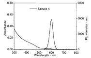
- Example 2 The absorption fluorescence spectra of Example 2 (Sample IV 4) and Example 5 (Sample IV 7) are shown in FIGS. 4 and 5, respectively.
- the transmission electron microscope images of Examples 1 and 2 coated with QD1 are shown in FIG.
- a is a transmission electron microscope image of Example 1 (Sample IV 3) and b is Example 2 (Sample IV 4).
- FIG. 7 shows transmission electron microscope images of Examples 3 to 6 (Samples 5 to 8) coated with QD2. From this, the thickness of the glass thin film and the total particle size can be read (see Table 1).
Landscapes
- Chemical & Material Sciences (AREA)
- Engineering & Computer Science (AREA)
- Nanotechnology (AREA)
- Materials Engineering (AREA)
- Physics & Mathematics (AREA)
- Organic Chemistry (AREA)
- Crystallography & Structural Chemistry (AREA)
- Inorganic Chemistry (AREA)
- Condensed Matter Physics & Semiconductors (AREA)
- General Physics & Mathematics (AREA)
- Life Sciences & Earth Sciences (AREA)
- Composite Materials (AREA)
- Manufacturing & Machinery (AREA)
- Optics & Photonics (AREA)
- Biophysics (AREA)
- Luminescent Compositions (AREA)
- Electroluminescent Light Sources (AREA)
Abstract
本発明は、耐久性が高くて小さく、また高輝度の量子ドット蛍光性微粒子を提供することを目的とする。さらに、それをバイオ分野の蛍光試薬、電子材料分野等に応用するための手法を示すことも本発明の目的とする。 Cd及びSeを含む量子ドットが、平均膜厚3nm以下のシリコンアルコキシドから作られたなるシリカガラスを含む薄膜にでコートされてなる蛍光性微粒子。当該蛍光性微粒子は、Cd及びSeを含む量子ドットを、疎水性雰囲気中で一定時間、アルコキシドとともに攪拌することでシラン化する工程を備える方法により作製することができる。なお、当該方法においては、上記シラン化工程の後、逆ミセル法等を用いてシリカガラス層を徐々につける工程を含むことが好ましい。
Description
本発明は、高発光効率の量子ドットをゾル-ゲル法によって作製したシリカガラスで覆った蛍光性微粒子、並びにその作製法及び応用に関するものである。
希土類イオン、遷移金属イオン等を無機材料に分散させた蛍光体は、有機色素に比べると耐久性に優れているため、従来より照明、ディスプレイ等に使用されてきた。しかし、その輝度及び演色性は必ずしも充分ではなかったため、それらを凌ぐ蛍光体が要望されていた。これを実現する可能性が高い新しい高性能蛍光体として、量子ドット(直径2~10nm程度、「半導体ナノ粒子」又は「半導体超微粒子」と呼ばれることもある)が近年、大変、注目されている。量子ドットは、同一波長の紫外線を照射した場合でも粒径に応じて様々な波長の明るい蛍光を発するため演色性に優れ、発光の減衰時間が短いので輝度を高くできるためである。量子ドットを注意して作製すれば、粒子1個1個の発光を別々に検出及び分光できるほどに輝度が高いために、ディスプレイ及び照明以外に、生体分子に結合させて蛍光試薬として生命の仕組みの解明、病気の診断等に用いる応用分野が大きく発展しようとしている。
このような蛍光体となる量子ドットは、主にII-VI族半導体(硫化カドミウム(CdS)、セレン化亜鉛(ZnSe)、セレン化カドミウム(CdSe)、テルル化亜鉛(ZnTe)、テルル化カドミウム(CdTe)、これらの混晶等)及びIII-V族半導体(リン化インジウム(InP)等)である。これらの半導体は直接遷移を示し、発光寿命が約10ナノ秒と、禁制遷移の性格をもつ希土類イオン又は遷移金属イオンを用いた蛍光体よりも約5桁短く、このためにはるかに高輝度の蛍光が得られる。
このように高輝度発光する量子ドットについては、水溶液中で合成する方法(親水性の量子ドットが合成される)と、水を高度に排除した有機溶液中で、高温で合成する方法(疎水性の量子ドットが合成される)の2つがある。量子ドットは比表面積が大きいために、表面エネルギーを下げようとして溶液中では徐々に凝集して発光効率が低下する。このため、どちらの方法によって合成された量子ドットでも、溶液のままでは応用しにくいという問題があった。これを解決するには、量子ドットを透明なマトリックスで覆い、種々の環境下で長期にわたって初期の特性を維持する材料とする必要がある。そのためのマトリックスとしては、ガラスと有機高分子材料の2つが挙げられる。このなかでもガラスは、有機高分子と比較して透明性が高く、紫外線照射に強い。また、ガラスはその網目構造のために、水分及び酸素を通しにくく、分散した量子ドットの劣化を長期にわたって防ぐことができる。このためのガラスの作製には、ゾル-ゲル法が有利である。なぜならば、ゾル-ゲル法では、常温常圧付近の穏やかな条件下でガラス化を進めることが出来るので、作製法を工夫すれば量子ドットは溶液法で合成された直後の高い発光効率を保持したまま、透明なガラス中に分散固定されるからである。
ここで、ゾル-ゲル法について説明を加える。ゾル-ゲル法は、一般式M(OR)n(但し、Mは金属;Rは低級アルキル基(特に炭素数が5以下のアルキル基)又はその誘導体;nは2~4の整数である。ここでORはアルコキシ基と呼ばれる。)で表されるアルコキシドを加水分解してM(OH)n(M及びnは前記に同じである)とした後、脱水縮合によって-M-O-M-の形の構造を形成する。n=4のアルコキシドは、結合手が4つあるので4官能のアルコキシドと呼ばれる。この4官能の金属アルコキシドにおいて、MがSiの場合(シリコンアルコキシド;Si(OR)4)が最も良く知られており、加水分解、脱水縮合が完結すると、≡Si-O-Si≡の3次元網目構造を持つシリカガラスが出来上がる。但し、脱水縮合は、数百℃の高温で長時間保持することでようやくほぼ完結する。一方で、室温付近でも不完全ながら反応は進行するので、シリカガラス類似の性質を示すガラスが出来上がる。文献では、このように低温で反応させたものでも、シリカガラスと呼ぶことが多い。シリカガラスは、炭素からなる有機高分子に比べると堅い3次元の網目構造を有するため丈夫であり、また物質の拡散係数が小さく、中に入っているものを保護する優れた性質を持つことが知られている。4官能のシリコンアルコキシドの中でも、Rが全てエチル基のもの(Si(OC2H5)4)が最も良く知られており、オルトケイ酸テトラエチル、テトラエトキシシラン、テトラエトキシオルソシリケートと呼ばれる。本願明細書では、これをTEOSと略する。
4官能のシリコンアルコキシドの1つ又は2つのアルコキシ基をアルキル基(又はその誘導体)Xで置換したものは有機アルコキシシラン又はシランカップリング剤と呼ばれ、式(I):
Xn-Si(OR1)4-n (I)
で表される。上記式(I)中、Xとしては、CH2=CH-で示される基、オキシランを含む基、H2NCmH2m-で示される基、CH2=C(CH3)COOCpH2p-で示される基、HSCqH2q-で示される基、又はフェニル基(但し、mは1~6の整数、pは1~5の整数、qは1~10の整数)が例示される。R1は低級アルキル基で、nは1又は2である。有機アルコキシシランは、(4-n)官能(nは1又は2)のアルコキシドである。有機アルコキシシランもゾル-ゲル反応によって固化し、できたものはガラスと呼ばれることがある。しかし、結合手が高々3つのために物質の拡散を抑える力が4官能のシリコンアルコキシドから作ったガラスよりも弱く、有機高分子の性質を有する。有機アルコキシシランを用いて作られた固体材料は、有機無機ハイブリッド材料と呼ばれることがある。
Xn-Si(OR1)4-n (I)
で表される。上記式(I)中、Xとしては、CH2=CH-で示される基、オキシランを含む基、H2NCmH2m-で示される基、CH2=C(CH3)COOCpH2p-で示される基、HSCqH2q-で示される基、又はフェニル基(但し、mは1~6の整数、pは1~5の整数、qは1~10の整数)が例示される。R1は低級アルキル基で、nは1又は2である。有機アルコキシシランは、(4-n)官能(nは1又は2)のアルコキシドである。有機アルコキシシランもゾル-ゲル反応によって固化し、できたものはガラスと呼ばれることがある。しかし、結合手が高々3つのために物質の拡散を抑える力が4官能のシリコンアルコキシドから作ったガラスよりも弱く、有機高分子の性質を有する。有機アルコキシシランを用いて作られた固体材料は、有機無機ハイブリッド材料と呼ばれることがある。
量子ドットを分散したガラス蛍光体として本発明者らは、バルク状のガラス(特許文献1)、ガラス微粒子(特許文献2~4)、並びにガラス薄膜(特許文献5)を開発した。このうち、ガラス微粒子(粒径10nm~2μm、粒子が完全な球形でない場合、例えばラグビーボール型(対称軸方向に長い回転楕円体)、パンケーキ型(偏平な回転楕円体)等の場合は、本願明細書では3つの慣性主軸の長さの平均を粒径と定義する。完全な球の場合は直径が粒径となる)は、ディスプレイ、照明等の発光デバイス用の粉体状の蛍光体として用いることができるほかに、生体分子に結合して蛍光試薬として用いる用途が重要である。以下では、典型例として、この蛍光性のシリカガラス微粒子に限定して記述する。
本発明者らによる上記の特許文献2~4では、アルコキシドを加水分解及び脱水縮合させるというゾル-ゲル法が用いられる。その中でも、逆ミセル法(油相中に分散した微小水玉中でゾル-ゲル法を進行させる方法で、水分散性の量子ドットを予め水玉中に分散させておく)又はストーバー法(加水分解したアルコキシドを量子ドット表面に降り積もらせる)を用いて、複数の量子ドットを、シリカガラス微粒子中に高い発光効率(20%以上)で分散させる技術が重要である。
ここでバイオ分野での応用可能性を探ると、粒径は、タンパク質が10nm程度、リボソームが25nm程度、ウイルスが100nm程度、赤血球が7μm程度であるから、広い範囲の応用に供するためには蛍光試薬に使う微粒子は小さいほど有利である。このためには、量子ドットをできるだけその蛍光特性を保ちつつ薄いガラスで覆うことが必要となる。この際、ガラスは有機アルコキシシランからなるものではなく、4官能のシリコンアルコキシドから作られたシリカガラスが最も好ましい。量子ドットは、最大で粒径が10nm程度の大きさなので、得られるガラスコート蛍光性微粒子の大きさは、15nm以下、平均ガラス膜厚にして3nm以下であることが好ましい。このとき、できるだけ膜厚を薄くするために、量子ドットは有機アルコキシシラン、高分子等を介さずにできるだけ発光特性を保ったまま、直接、4官能のシリコンアルコキシドから合成されたガラスに被覆されているのが好ましい。ところが、そのような蛍光性微粒子で、しかも小さく、発光効率が高いものを合成する手法は、以下で詳述するように知られてはいなかった。
量子ドットをガラスで覆うと丈夫になることは、容易に予想された。このため、発光効率の高い量子ドットが作られるようになった直後の西暦2000年頃から世界中で競って、ガラスマトリックスで覆うための研究が始まった。本発明者らは、そのなかでも特に、CdとSeを含む量子ドットが分散されたシリカガラス微粒子として報告されているものに注目し、その粒径及び発光特性を調べた。
CdSe/ZnS量子ドットをゾル-ゲル法でガラス中に分散固定した蛍光性のシリカガラス微粒子、及びその作製方法は、バベンディらによって報告されている(非特許文献1)。この作製方法は、予め有機溶媒中で合成した量子ドットの表面を、アミノ基を有するアルコキシド(3-アミノプロピルトリメトキシシラン)及びアミノ基を有するアルコール(5-アミノ-1-ペンタノール)で覆い、別途用意した直径数百nmのシリカガラス微粒子の表面に厚さ50nm程度の層として接着させるという方法である。この方法によれば、量子ドットを含まないシリカガラス微粒子の表面に、量子ドットを含有するゾル-ゲルガラス層がコートされた構造の蛍光性ガラス微粒子が得られる。しかし、ガラス微粒子の表層付近にのみ量子ドットが存在し、ガラス微粒子の核には量子ドットが含まれていないため、ガラス微粒子中の量子ドットの分散濃度を高めることができなかった。また、発光効率は13%程度であった。
別の作製方法として、CdSe/ZnS量子ドットの表面にチオール基を有するアルコキシド(有機アルコキシシランの一種)等を成長させ、1個のシリカガラス微粒子中に1個の量子ドットを含むシリカガラス微粒子を作る方法が報告されている(非特許文献2)。この場合の発光効率は、5~18%と報告されている。他にも、類似の方法で作製したCdSe/ZnS量子ドット1個を含む粒径30nm~1μmのシリカガラス微粒子が報告されているが発光効率については記載がない(非特許文献3)。
マイヤーリンクらは、1個の量子ドットを1個のシリカガラス微粒子に導入することを目的として、CdSe/CdS/Cd0.5Zn0.5S/ZnS(CdSeを核としてCdS、Cd0.5Zn0.5S及びZnSが順次コートされている)量子ドットを、逆ミセル法によってシリカガラス微粒子(直径35nm程度)中に導入した(非特許文献4)。しかしながらそのメカニズムの検討から、加水分解されたアルコキシドは、量子ドットに対する親和性が高いために作製時に量子ドット表面に配置されていた配位子を置き換え、これによって発光が消光されると記載されている。このため、量子ドットが1個だけ入っているシリカガラス微粒子においてその発光効率は作製直後に急激に低下し、さらには徐々に低下して1週間後にはシリカガラスに入れる前の状態の2%(絶対値としては始めの60%から1.2%へ低下)の程度となる。このようなシリカガラスによる消光効果をなくすために、特別に厚いシェルを作った量子ドットを用いると、発光効率は上昇する。しかし、このように特別に厚いシェルを作った量子ドットは、粒径が大きくなり、バイオ分野への応用には適さない上に、そのような量子ドットを作製するのは困難となる。
水分散性のCdSe量子ドット(クエン酸コート)を作製し、それを複数個、シリカガラス微粒子中に導入した研究も知られている(非特許文献5)。しかし水分散性のCdSe量子ドットは発光効率が0.1~0.15%と極端に低い。量子ドットをシリカマトリックス中へ導入したときの発光効率については記述がないが、普通は発光効率がさらに減少するので、これを蛍光体と呼ぶことはできない。また、同じく水分散性のCdSe量子ドットを逆ミセル法によってシリカ粒子中に導入した比較的最近の文献(非特許文献6)の場合も、発光効率は高々1.48%であり、蛍光体と呼ぶことはできない。特許文献6に例示されるように、蛍光体と呼ぶことができる凡その目安は発光効率20%以上である。
逆ミセル法を用いる方法として、アミノプロピルトリメトキシシラン(有機アルコキシシランの一種)でCdSe量子ドットを覆った後、アンモニアとTEOSとを加える方法が報告されている(非特許文献7)。さらにCdSe/ZnS量子ドットについては、ポリエチレングリコールで修飾したのち、アンモニアとTEOSとを加えている。この場合の発光効率は最大で17%程度であり、透過電子顕微鏡像を見ると量子ドットが含まれないガラスビーズも散見される。
同じグループから、量子ドットと磁性ナノ粒子が分散したガラスビーズについても報告されている。(非特許文献8)。この場合も逆ミセル法を利用しているが、作製されるガラスビーズの大きさ(粒径)は50nm程度、発光効率は最大で4.8%と報告されている。
さらに逆ミセル法によって、量子ドットを油相に分散させてTEOSを加えた後、30分程度の攪拌の後アンモニアを添加することで、直径30nm程度のガラスビーズを得ることもできる(非特許文献9)。ここでは発光効率の報告はないが、報告されている蛍光スペクトルにノイズが多いため、発光効率は高くないと予想される。我々の追加実験でも、この方法では高い発光効率が得られないことがわかっている。この研究は同じ研究者によって続けられたが、得られたガラスビーズの直径は30nm程度、発光効率については報告されていない(非特許文献10)。
さらに、4官能のシリコンアルコキシドを全く使わずに、有機アルコキシシランのみで覆った量子ドットも報告されている(非特許文献11)。この場合は、リガンド(トリオクチルフォスフィンオキサイド等)で安定化されたCdSe/ZnSを、3種類の有機アルコキシシランで順に覆うことで、それぞれ親水化、シェル形成、表面の機能化を行っている。このため、サイズも大きくなり17.4±2.1nmと報告されている。TEM像及び量子ドットの第一吸収ピーク波長から見積もられる粒径はおよそ3nmであるから、量子ドットの周りのコートの厚みは7nm以上となる。
Cd及びSeを含む量子ドットは、水溶液で作る親水性のものと有機溶液で作る疎水性のものが知られる。疎水性のものの方が、高発光効率で蛍光スペクトル幅が狭く、また耐久性に優れている。先の特許文献4では、親水性のCdTe量子ドット等をガラスビーズに入れている。この場合は、スペクトル幅(半値全幅)が赤色領域(640nm)で60nmを超える程度に広くなる。Zn、Se等を混ぜるなどして三元系にすると、このスペクトル幅はさらに広がる。また、ゾル-ゲル反応のスピードが制御されないので、ガラスビーズ中に入る量子ドットの数は1個を超えており、平均粒径15nm以下のものを作ることが出来なかった。さらに、量子ドットはガラスビーズ全体に分布し、シリカガラスの保護層を持っていない。また大量のTEOSを導入するため、溶液の粘度が上がり、作製されるガラスビーズのサイズ分布も、数十nm-数μmと幅広かった。
このように、Cd及びSeを含む量子ドットを平均膜厚で3nm以下、平均粒径にして15nm以下のアルコキシドから作られたシリカガラス薄膜でコートされた蛍光性微粒子は知られていなかった。
一方で、線状の高分子を用いて複数の量子ドットの集合体を作る方法が最近、報告されている(非特許文献12)。この方法で作製するポリマー粒子は、動的光散乱によって測定した平均粒径が112nmと報告されているが、粒径100nm以下の量子ドット集合体を作るのは現状では困難である。この集合体の表面をさらにガラス被覆することも可能であるが粒径がさらに増加する。また、一般に、ポリマーを含まないガラス材料のほうが耐久性に優れており、またCdの溶出量も少ないことから、ポリマーを用いずにガラス材料を作ることが要求されている。
さらに、作製した材料をin vivo(生体内)のイメージングに用いる場合は、生体内の物質による吸収が少ない波長域を選ぶことが重要である。このためには、ヘモグロビン、水等の吸収域を避けて、「生体の窓」と呼ばれる波長範囲650~1000nmの波長で発光を示すことが重要である(http://www.aist.go.jp/aist_j/press_release/pr2009/pr20090908/pr20090908.html)。この波長域で発光する量子ドットは、市販されている。しかし、公知の作製法では、発光効率が20%以上を示す量子ドットを得ることが出来なかった。
チャン、ツィンマー、ストロー、ステッケル、ジャイン、バベンディ、アドバンスド マテリアルズ、16巻、2092頁(2004)
ゲリオン、ピノー、ウィリアムス、パラック、ザンチェト、ワイス、アリビサトス、ジャーナル オブ フィジカルケミストリー ビー、105巻、8861頁(2001)
ナン、ムルバニー、アンゲバンテ ヒェミー インターナショナル エディション、43巻、5393頁(2004)
クール、シューネベルト、ヒルホスト、ドネガ、ハート、ブラーデレン、バンマエケルベルク、マイヤーリンク、ケミストリー オブ マテリアルズ、20巻、2503頁(2008)
ロガッシュ、ナゲーシャ、オストランダー、ギールジッヒ、コトフ、 ケミストリー オブ マテリアルズ、12巻、2676頁(2000)
チュー、ソン、シュ、ジャーナル オブ ナノパーティクル リサーチ、10巻、613頁(2008)
セルバン、タン、イング、アドバンストマテリアルズ、17巻、1620頁(2005)
イ、セルバン、リー、パパエフィミウ、クンダリア、イング、ジャーナル オブ アメリカン ケミカル ソサエティ、127巻、4990頁(2005)
ダーバンディ、トマン、ナン、ケミストリー オブ マテリアルズ、17巻、5720頁(2005)
ダーバンディ、ウルバン、クルーガー、ジャーナル オブ コロイド アンド インターフェース サイエンス、351巻、30頁(2010)
ゼレフ、オオバ、バカローバ、ジャーナル オブ アメリカン ケミカル ソサエティ、128巻、6324頁(2006)
ヤング、デイブ、ガオ、ジャーナル オブ アメリカン ケミカル ソサエティー、130巻、5286頁(2008)
Dmitri V. Talapin, Andrey L. Rogach, Ivo Mekis, Stephan Haubold, Andreas Kornowski, Markus Haase, Horst Weller, Colloids and Surfaces A, 202, 145(2002).
Dmitri V. Talapin, Andrey L. Rogach, Andreas Kornowski, Markus Haase, and Horst Weller, NANO LETTERS, 1, 207(2001).
Z. Adam Peng and Xiaogang Peng, J. Am. Chem. Soc., 123, 1389(2001).
C. B. Murray, D. J. Norris, M. G. Bawendi, J. Am. Chem. Soc., 115, 8706(1993).
B. O. Dabbousi, J. Rodriguez-Viejo, F. V. Mikulec, J. R. Heine, H. Mattoussi, R. Ober, K. F. Jensen, and M. G. Bawendi, J. Phys. Chem. B, 101 (46), 9463(1997).
Lianhua Qu and Xiaogang Peng, J. Am. Chem. Soc., 124, 2049(2002).
Xinhua Zhong, Yaoyu Feng, and Yuliang Zhang, J. Phys. Chem. C, 111, 526(2007).
Renguo Xie, Ute Kolb, Jixue Li, Thomas Basche, and Alf Mews, J. Am. Chem. Soc., 127,7480(2005).
Robert E. Bailey and Shuming Nie, J. Am.Chem. Soc., 125, 7100(2003).
S. Jun, E. Jang, J. E. Lim, Nanotechnology, 17, 3892(2006).
ケミストリー オブ マテリアルズ、15巻、2854頁、2003年
ジャーナル オブ ルミネッセンス、128巻、1896頁(2008)
発明者らは、これまで主にCdTe量子ドットを用いて種々の形態(バルク体、薄膜、ファイバー状、微粒子)のシリカガラスコート量子ドットを作製してきた。その中で、作製したシリカガラス微粒子を蛍光試薬としてバイオの分野で応用する場合には、蛍光特性の評価の条件が、他の材料作製の場合とは通常、大きく異なる。
シリカガラス微粒子は粒径が100nm程度又はそれ以下であれば散乱が少ないので、溶液に分散させたまま、光路長1cmの石英セルに導入し、それを汎用の吸光分光光度計及び蛍光分光光度計で測定する。これによって、波長ごとの吸光度及び蛍光強度を得る。散乱の影響が懸念される場合には積分球を用いるが、この時は吸光度及び蛍光強度ともに散乱がない場合に比べて誤差が大きくなる。この場合も最近は汎用の測定装置が市販されている(例えば、浜松ホトニクス(株)のC9920-02等)。
合成時の量子ドットの濃度は、通常1~10μM(マイクロモル/リットル、量子ドットの数であり、それを構成する原子の数ではない)の程度であり、これをそのまま冷暗所に保管する。発光効率の測定時には、この濃度では濃すぎるので、200~300nM程度に薄める。そうすると、汎用の吸光分光光度計又は蛍光分光光度計で最も測定しやすい信号量が得られる。溶媒は純水であることが多い。一方で、蛍光試薬として応用する際には、1個又は数個程度の量子ドットからの蛍光を別々に検出することが多く、その場合には量子ドットの濃度として高々10nMの程度となり、しかも生理食塩水のような高濃度の塩中に分散される。また、照射光強度も通常、10W/cm2以上の値となり、分光器の場合より桁違いに強い。このように、材料合成の観点から見ると極端に量子ドットの分散濃度が低く、さらに溶液中に多量の塩類が含まれる場合には、たとえガラスにコートされていても、特にCdTe量子ドットの場合は、急激に劣化することがわかってきた。このような劣化を抑えるためには、CdTe量子ドット以外の量子ドットを用いることが必要になる。
本発明は、背景技術で記した問題点およびガラスコートCdTe量子ドットに見出された劣化を解決するためになされたものであり、その目的は、耐久性が高くて小さく、また高輝度の蛍光性微粒子を提供することである。さらに、それをバイオ分野の蛍光試薬、電子材料分野等に応用するための手法を示すことも本発明の目的とする。
上記の課題を解決するために、まず希薄濃度で分散させた量子ドットの安定性について調べた。そうしたところ、CdとTeを主成分とする量子ドット等と比べて、CdとSeを含む量子ドットが最も優れていた。また、CdとSeを含む量子ドットは、蛍光スペクトル幅が狭く発光効率が高かった。このため、この量子ドットを用いることとした。但し、通常の方法で作製したこの量子ドットは、疎水性である。ゾル-ゲル法を用いて加水分解及び脱水縮合を行わせるためには、量子ドットは親水性であることが有利となる。そこで、以下の2つのステップからなる合成法を開発した。この合成法は、具体的には、図3に記載のような工程からなるものである。
ステップ1
CdとSeを含む量子ドットを分散した疎水性溶媒に、適量のシリコンアルコキシド(1)を添加して攪拌する。疎水性溶媒が、極僅かの水分を空気中から取り入れるので、シリコンアルコキシド(1)は、4つのアルコキシ基のうち1つだけが徐々に加水分解して、(RO)3-Si-OHとなる。この分子が、量子ドット表面に作製時に配位したリガンドを置換し、直接に量子ドットを覆うことがわかった。加水分解反応がゆっくりであれば、(RO)3-Si-OHは整然と並んで量子ドットを覆うので、発光効率の低下が抑えられる。
CdとSeを含む量子ドットを分散した疎水性溶媒に、適量のシリコンアルコキシド(1)を添加して攪拌する。疎水性溶媒が、極僅かの水分を空気中から取り入れるので、シリコンアルコキシド(1)は、4つのアルコキシ基のうち1つだけが徐々に加水分解して、(RO)3-Si-OHとなる。この分子が、量子ドット表面に作製時に配位したリガンドを置換し、直接に量子ドットを覆うことがわかった。加水分解反応がゆっくりであれば、(RO)3-Si-OHは整然と並んで量子ドットを覆うので、発光効率の低下が抑えられる。
ステップ2
次に、この工程では、表面シラン化された量子ドットの表面に、薄いシリカガラス層を付与する。
次に、この工程では、表面シラン化された量子ドットの表面に、薄いシリカガラス層を付与する。
このため、逆ミセル溶液(水が油相中にドロップレット状に分散)を作製する方法が例示される。これに、ステップ1で作製した量子ドット溶液を添加すると、量子ドットは疎水性溶媒からなる連続相に分散し、その後ドロップレット相に分配される。この後に、シリコンアルコキシド(2)を添加する。このステップで使用するシリコンアルコキシド(2)は、疎水性の連続相に分配されるので、ドロップレットとして分散している水に触れて徐々に加水分解する。また、量子ドット表面についたシリコンアルコキシド(1)も徐々に加水分解するため、量子ドットは親水性になり、水相に転換される。そののち、加水分解したステップ2で使用するシリコンアルコキシド(2)が徐々に水相に移動して量子ドット表面に堆積、脱水縮合する。この方法によれば、反応速度が遅いため、シリカガラスの厚みを細かく制御できる。また、均一な膜が形成される。さらに逆ミセル中なので、他の量子ドットと衝突して凝集することがなくなり、1個のガラスビーズ中に1個の量子ドットが分散する。また、量子ドットを含まない、空のガラスビーズの形成も抑えられる。
ステップ2は、上述の逆ミセル法に限定されるものではない。逆ミセル法を利用しない場合には、例えば、ステップ2において、シリコンアルコキシド(1)を少量、段階的に添加する等の工夫をして、空のガラスビーズの形成を防ぎ、量子ドット表面のガラス層形成を徐々に行って膜厚の制御をしやすくする等の工夫をすればよい。
本発明者らは、このように工夫されたゾル-ゲル法によって作製されたCdとSeを含む量子ドット分散蛍光性シリカガラス微粒子は、平均膜厚3nm以下のアルコキシドから作られたシリカガラスを含む薄膜でコートされた蛍光性微粒子を提供すること、その発光効率が20%以上であることを確認した。本発明者らは、このような知見に基づき、さらに研究を重ね、本発明を完成させた。
即ち、本発明は下記記載の高耐久性で高輝度の微小なシリカガラス薄膜コート量子ドット(蛍光性微粒子)と、そのゾル-ゲル法による作製法とを提供するものである。さらに、in vivo イメージングに用いることのできる長波長発光の量子ドットとそのシリカ薄膜コート手法を提供する。in vivoイメージングでは、生体内に量子ドットを入れるので、耐久性があってカドミウムの溶出が少ないことは、大変有利となる。
項1.Cd及びSeを含む量子ドットが、平均膜厚3nm以下のシリコンアルコキシドからなるシリカガラスを含む薄膜でコートされてなる蛍光性微粒子。
項2.前記量子ドットが、Cd及びSeを含むコアと、Zn及びSを含むシェルとからなる項1に記載の蛍光性微粒子。
項3.前記量子ドットの発光ピーク波長が650nm以上1000nm以下である、項2に記載の蛍光性微粒子。
項4.前記量子ドットが、シリコンアルコキシドからなるシリカガラスで直接にコートされている、項1~3のいずれかに記載の蛍光性微粒子。
項5.前記量子ドットが疎水性である、項1~4のいずれかに記載の蛍光性微粒子。
項6.前記量子ドットの蛍光スペクトルの半値膳幅が35nm以下である、項1~5のいずれかに記載の蛍光性微粒子。
項7.平均粒径が15nm以下である、項1~6のいずれかに記載の蛍光性微粒子。
項8.表面にCOOH基、NH2基、SH基及びこれらの塩、並びにポリエチレングリコール由来の基よりなる群から選ばれる少なくとも1種類を有する、項1~7のいずれかに記載の蛍光性微粒子。
項9.量子ドットの数が1個である、項1~8のいずれかに記載の蛍光性微粒子。
項10.発光効率が20%以上である、項1~9のいずれかに記載の蛍光性微粒子。
項11.蛍光試薬用である項1~10のいずれかに記載の蛍光性微粒子。
項12.電子材料用である項1~10のいずれかに記載の蛍光性微粒子。
項13.エレクトロルミネッセンス及び/又はカソードルミネッセンスを示す、項1~10のいずれかに記載の蛍光性微粒子。
項14.(1)Cd及びSeを含む量子ドット及びシリコンアルコキシドを含有する疎水性溶媒を1時間以上攪拌して疎水性量子ドットを作製する工程
を備える、項1~13のいずれかに記載の蛍光性微粒子の製造方法。
項15.さらに、
(2)作製した疎水性量子ドットを、親水性に転換する工程
を備える、項14に記載の蛍光性微粒子の製造方法。
項16.前記工程(2)が、作製した疎水性量子ドット、アルカリ性水溶液及びシリコンアルコキシドを、逆ミセル溶液に添加して1時間以上攪拌する工程である、項15に記載の蛍光性微粒子の製造方法。
項17.前記Cd及びSeを含む量子ドットが、溶液に含まれるCdの量をXミリモル、加えるSeのスピードをYミリモル/分としたときに、0.3X<Y<2Xの条件を含む工程で作製されたものである、項14~16のいずれかに記載の蛍光性微粒子の製造方法。
項1.Cd及びSeを含む量子ドットが、平均膜厚3nm以下のシリコンアルコキシドからなるシリカガラスを含む薄膜でコートされてなる蛍光性微粒子。
項2.前記量子ドットが、Cd及びSeを含むコアと、Zn及びSを含むシェルとからなる項1に記載の蛍光性微粒子。
項3.前記量子ドットの発光ピーク波長が650nm以上1000nm以下である、項2に記載の蛍光性微粒子。
項4.前記量子ドットが、シリコンアルコキシドからなるシリカガラスで直接にコートされている、項1~3のいずれかに記載の蛍光性微粒子。
項5.前記量子ドットが疎水性である、項1~4のいずれかに記載の蛍光性微粒子。
項6.前記量子ドットの蛍光スペクトルの半値膳幅が35nm以下である、項1~5のいずれかに記載の蛍光性微粒子。
項7.平均粒径が15nm以下である、項1~6のいずれかに記載の蛍光性微粒子。
項8.表面にCOOH基、NH2基、SH基及びこれらの塩、並びにポリエチレングリコール由来の基よりなる群から選ばれる少なくとも1種類を有する、項1~7のいずれかに記載の蛍光性微粒子。
項9.量子ドットの数が1個である、項1~8のいずれかに記載の蛍光性微粒子。
項10.発光効率が20%以上である、項1~9のいずれかに記載の蛍光性微粒子。
項11.蛍光試薬用である項1~10のいずれかに記載の蛍光性微粒子。
項12.電子材料用である項1~10のいずれかに記載の蛍光性微粒子。
項13.エレクトロルミネッセンス及び/又はカソードルミネッセンスを示す、項1~10のいずれかに記載の蛍光性微粒子。
項14.(1)Cd及びSeを含む量子ドット及びシリコンアルコキシドを含有する疎水性溶媒を1時間以上攪拌して疎水性量子ドットを作製する工程
を備える、項1~13のいずれかに記載の蛍光性微粒子の製造方法。
項15.さらに、
(2)作製した疎水性量子ドットを、親水性に転換する工程
を備える、項14に記載の蛍光性微粒子の製造方法。
項16.前記工程(2)が、作製した疎水性量子ドット、アルカリ性水溶液及びシリコンアルコキシドを、逆ミセル溶液に添加して1時間以上攪拌する工程である、項15に記載の蛍光性微粒子の製造方法。
項17.前記Cd及びSeを含む量子ドットが、溶液に含まれるCdの量をXミリモル、加えるSeのスピードをYミリモル/分としたときに、0.3X<Y<2Xの条件を含む工程で作製されたものである、項14~16のいずれかに記載の蛍光性微粒子の製造方法。
本発明の蛍光性微粒子は、耐久性がある量子ドットをさらに薄いシリカガラス薄膜で覆っている。また、もとの発光効率を保つための工夫もされている。本発明の蛍光性微粒子は、全体の粒径が15nm以下であるため、蛍光試薬として広い分野への応用が可能である。なお、量子ドットがシリカガラスで覆われていることは、まず透過型電子顕微鏡による観察でその膜厚を確認した後、分析電子顕微鏡による該当部分の解析によってケイ素と酸素が含まれることから確認することができる。また、試料を真空乾燥して粉体にした後に、粉末X線回折(CuのKα線、1.5406オングストロームを照射)によって角度(2θ)が23度の付近に半値全幅5度又はそれ以上の広い回折ピークが現れることからも確認できる。なお、シリカガラス膜厚が0.5nmよりも薄い場合には、直接、透過電子顕微鏡でシリカガラス層の存在を確認することが難しくなる。しかしながら、作製時に疎水性の量子ドットがその発光効率及び分散性を保ちながら水相に転換することから、シリカガラスにコートされたことを確認することが出来る。さらに、分析電子顕微鏡により、量子ドットの表面付近にSiの存在を確認することが出来る。また、蛍光光子相関法や光散乱法などの光学的手法によっても、もとの量子ドットよりも粒径が大きくなったことを確認できる。
本発明によって作製されるものは、Cd及びSeを含有する量子ドット1個が、平均膜厚3nm以下のシリカガラスを含む薄膜でコートされた蛍光体である。以下、1.量子ドットの作製、2.表面シラン化(ステップ1)、3.シリカガラス薄膜コートと表面修飾(ステップ2)、4.評価及び5.用途の順に説明する。
1.量子ドットの作製
本発明では、安定性が高く、且つ、蛍光スペクトル幅が狭く発光効率が高いという特徴を持つ、Cd及びSeを含有する量子ドットを使用する。まず、Cd及びSeを含有する量子ドットの作製法を説明する。
本発明では、安定性が高く、且つ、蛍光スペクトル幅が狭く発光効率が高いという特徴を持つ、Cd及びSeを含有する量子ドットを使用する。まず、Cd及びSeを含有する量子ドットの作製法を説明する。
本発明で使用する量子ドットとしては、CdとSeを含むものであれば制限はなく、必ずしもCd及びSeのみからなる必要はない。ただし、希土類イオン、遷移金属イオン等をドープした量子ドットは、希土類イオン及び遷移金属イオンからの蛍光が得られ、量子ドットが持つ蛍光特性が得られにくいので、希土類イオン及び/又は遷移金属イオンをドープしていない量子ドットが好ましい。具体的にはCdSe、CdSe/ZnS(ZnSでコートされたCdSe量子ドット)、CdSe/CdS/Cd0.5Zn0.5S/ZnS(CdSeを核としてCdS、Cd0.5Zn0.5S及びZnSが順次コートされた量子ドット)、合金組成のCdSexTe1-x(0<x<1)等が例として挙げられる。なかでも、表面にZnS、ZnSe、CdS等のシェルを有しているものが優れている。特に、Zn及びSを含むシェルを有しているものが好ましい。このシェルは、Cd、Zn、Se、S等の組成がシェルの厚み方向で変化する傾斜組成であってもよい。
このようなCd及びSeを含む量子ドットの作製方法としては、以下の代表的な10個の公知の方法が知られている(非特許文献13~22)。
これらの方法で作製される量子ドットの平均粒径はおよそ2~9nmである。
いずれの場合も、水を排除した有機溶液中での高温の反応を用いる。この第1工程で作製した量子ドット表面の配位子を、以下の第2工程(ステップ1)で加水分解したシリコンアルコキシド(1)に置き換えるので、この工程の配位子は結合エネルギーが小さいものが望ましい。具体的な配位子として、アルキル基を持つリン酸化合物(トリオクチルフォスフィン、トリオクチルフォスフィンオキサイド等)、アルキルアミン(ヘキサデシルアミン、オクタデシルアミン、オレイルアミン、ミリスチルアミン、ラウリルアミン等)、オレイン酸等が挙げられる。
ただし、これらの作製方法では、発光ピーク波長が650~1000nmの量子ドットは得られない。
さらに蛍光波長650~1000nmの量子ドットを作製するためには、コアとなるCdSeの作製法を開発し、セレン含有原料の注入スピード、温度、反応時間等を最適化する必要がある。
例えば、不活性雰囲気下(窒素雰囲気下、アルゴン雰囲気下等)、酸化カドミウム0.3~0.7mmol(より好ましくは、0.5~0.6mmol)、オクタデシルホスホン酸150~200mg(より好ましくは175~185mg)、トリオクチルアミン(TOA)3~10mL(より好ましくは4~6mL)をガラス容器に入れた場合は、320~330℃に加熱して酸化カドミウムを完全に溶解してカドミウム溶液を作製する。これとは別に、セレン粉末0.5~2mmol(より好ましくは0.8~1.2mmol)を1mLのトリオクチルホスフィン(TOP)に溶解し、TOPSe(TOPにセレンが結合したもの)を作製する。ガラス容器中のカドミウム溶液を320~330℃(より好ましくは322~327℃)に保ちつつ、激しく攪拌しながら0.15~0.4mL/min(より好ましくは0.2~0.3mL/min)のスピードでTOPSeを注入する。4~8分(より好ましくは5~7分)反応させた後、室温付近まで冷却し、さらに精製することで、コアを得ることができる。この中でも特に、注入スピードを調整することが、今までの多くの研究で見逃されてきた大切なポイントである。ゆっくり注入することで核形成を抑え、原料を核成長に使うことで、大きな量子ドットを得ることができる。注入スピードは、注入するTOP溶液中のTOPSeの濃度に反比例して変えればよい。また、予め容器の中に分散させているカドミウムの量に比例して、変えればよい。一般的には、溶液に含まれるCdの量をXミリモル、これに注入するSeのスピードをYミリモル/分としたときには、
0.3X<Y<2X
とするのが良く、さらに
0.5X<Y<1.5X
とするのがさらに好ましい。発光波長を700nmよりも長くする場合には、TOPSe注入の際に、さらにTeをTOPTe(TOPにTeが結合したもの;TOPにTe粉末を溶かすことで得られる)として添加するのが好都合である。
0.3X<Y<2X
とするのが良く、さらに
0.5X<Y<1.5X
とするのがさらに好ましい。発光波長を700nmよりも長くする場合には、TOPSe注入の際に、さらにTeをTOPTe(TOPにTeが結合したもの;TOPにTe粉末を溶かすことで得られる)として添加するのが好都合である。
コアであるCdSeの作製方法は、上記に限定されることはなく、Cd原料、Se原料、Cd又はSeを溶解させる溶媒の種類等について、必要に応じて適宜変更すればよい。例えばCd原料は、Cd(CH3)2のヘキサン溶液を用いることができる。溶媒は、トリオクチルホスフィンオキシド(TOPO)、ヘキサデシルアミン(HDA)等を用いることができ、この場合の反応温度は、290~295℃である。HDAは溶媒及びCdSeに付くリガンドの2つの役割がある。溶媒としてステアリン酸を用いる場合は、反応温度として300℃程度がよい。
コアはCdとSeのみからなるものが、蛍光スペクトル幅を狭くし、また耐久性を上げるためには好ましい。コアにさらにTe等を含有させると、長波長発光が得られる。その場合でも、耐久性と蛍光スペクトル幅を保つためにはTe等他元素の含有量は30mol%以下であることが好ましく、さらに10mol%以下であることがより好ましい。
量子ドットのコアは、100℃程度の水溶液で作る場合(親水性のコアが出来る)と300℃程度の高温の有機溶液で作る場合(疎水性のコアが出来る)の2通りがある。耐久性が高く、蛍光スペクトル幅の狭い量子ドットを作るためには、有機溶液法が好ましい。先に述べたとおり、上記非特許文献13~22も有機溶液法で作製している。一般に、有機溶液法で作製したコアのほうが、そのあとシェルを付けた時の発光効率が高くなる。
このコア作製のあとで、CdSeからなるコアの表面にシェルをつけて波長650~1000nmの発光を得るためには、コアの段階での発光波長が618nm以上であることが好ましく、620nm以上であることがより好ましい。得られる量子ドットの平均の大きさは、典型的な場合で9~11nmである。但し、球形でない場合には、3つの慣性主軸方向のサイズの平均値を持って1つの粒子の大きさとする。シェルの作製に際しては、Cd、Zn及びSからなるシェルを形成させる場合を例にとると、CdとZnの塩、例えば、酢酸塩をCdとZnの比率をおよそ1:1にして加えるのが好都合である。格子定数の関係等から、始めCdが優先的にCdSeコアに付き、あとからZnが付く。このときの組成から、量子ドットはCdSe/CdxZn1-xSと書くこともある。Sは、上記のSe及びTeの場合と同様に、TOPS(TOPに粉末のSを溶かしたもの)を用いてCd又はZnと反応させればよい。
シェル作製方法も、上記に限定されることはなく、必要に応じて適宜選択する。例えば、ZnS単独のシェルをつける場合は、亜鉛の原料としてジエチル亜鉛、硫黄の原料としてヘキサメチルジシラチアン(慣用名 チオビス(トリメチルシラン))(Hexamethyldisilathiane (Thiobis(trimethylsilane)))を用いることができる。
2.表面シラン化(ステップ1)
上述の方法で、Cd及びSeを含む量子ドットを作製することができる。但し、この量子ドットは、水を排除した有機溶媒中で作製されるため、疎水性である。ゾル-ゲル法を用いて加水分解及び脱水縮合を行わせるためには、量子ドットは親水性であることが有利となる。このため、この工程では、量子ドット表面をシリコンアルコキシド(1)でシラン化する。
上述の方法で、Cd及びSeを含む量子ドットを作製することができる。但し、この量子ドットは、水を排除した有機溶媒中で作製されるため、疎水性である。ゾル-ゲル法を用いて加水分解及び脱水縮合を行わせるためには、量子ドットは親水性であることが有利となる。このため、この工程では、量子ドット表面をシリコンアルコキシド(1)でシラン化する。
量子ドットの発光効率を保ったままシリカガラスコートすることは、この数年の学会の関心事であったから、疎水性量子ドットがシリカガラスでコートされるとき、もとの表面配位子が取れるのか否かについての論争が続いていた。そして公知の非特許文献4により、加水分解されたシリコンアルコキシドは量子ドットに対する親和性が高く、作製時に表面に接着していたアルキルアミンなどの配位子(リガンド)を置換してコートすることが示された。ところが、アルキルアミン配位子が表面欠陥をなくして発光効率を向上させるのに対して、一部分が加水分解したシリコンアルコキシドから成る配位子(例えば(Et-O)3-Si-O-)には消光作用があるために、発光効率が急激に低下すると報告されている。その一方で、なぜ加水分解したシリコンアルコキシドに消光作用があるのかは不明とされていた。
一方で、発光効率を保つためには、量子ドットの表面を配位子が密に覆うことが必要とされている。このためには、非特許文献13に説明があるように枝分かれのない1級のアルキルアミンが有用である。
これらの文献をもとに被覆の条件を探ると、シリコンアルコキシドの加水分解速度を遅く、量子ドットの濃度を薄く、また、反応時間を長く取れば、シリコンアルコキシド加水分解物への表面置換が終わった後も量子ドットの発光効率がほとんど低下しないことを見出した。つまり、加水分解されたシリコンアルコキシドそのものに消光作用があるわけではなく、量子ドットの表面にシリコンアルコキシドが乱雑に密集すること、表面への接着数が充分でないこと等が、消光に繋がることが判明した。これにより、疎水性溶媒中でシリコンアルコキシド(1)を用いて表面被覆した後、別のシリコンアルコキシド(2)を含む大量の水と接触させることで、量子ドットの集合体を形成できることを見出した。このときのシリコンアルコキシド(1)の表面被覆の条件を最適化し、表面シラン化を行った。さらに、次の項(シリカガラス薄膜コートと表面修飾)で述べるように少量の水と徐々に反応させることで、薄いシリカガラス層を形成できる。
具体的には、まず、先の項で作製した量子ドットを疎水性溶媒に分散させる。疎水性溶媒は特に限定されないが、トルエン、クロロホルム、ヘキサン等が例示され、とくにトルエンが好ましい。このときの量子ドットの濃度は0.1~20μM(マイクロモル/リットル)が好ましく、さらに0.5~10μMが好ましく、1~5μMが最もよい。
次に、当該分散液に、式(II):
Si(OR2)4 (II)
(式中、4個のR2は同じか又は異なり、それぞれ低級アルキル基(特に炭素数が5以下のアルキル基)又はその誘導体である)
で示されるシリコンアルコキシド(1)を添加する。
Si(OR2)4 (II)
(式中、4個のR2は同じか又は異なり、それぞれ低級アルキル基(特に炭素数が5以下のアルキル基)又はその誘導体である)
で示されるシリコンアルコキシド(1)を添加する。
ここでは、疎水性溶媒が、極僅かの水分を空気中から取り入れるので、シリコンアルコキシド(1)は、4つのアルコキシ基のうち1つだけが徐々に加水分解して、(R2O)3-Si-OHとなる。この分子が、量子ドット表面に作製時に配位したリガンドを置換し、直接に量子ドットを覆う。加水分解反応がゆっくりであれば、(R2O)3-Si-OHの水酸基が量子ドット表面方向に配置され、整然と量子ドットを覆うので、発光効率の低下が抑えられる。
式(II)で示されるシリコンアルコキシド(1)としては、テトラエトキシシラン(TEOS)、テトラメトキシシラン等が例示され、TEOSが好ましい。シリコンアルコキシド(1)の濃度は、0.004~0.1μMが好ましく、さらに0.008~0.05μMが好ましく、0.01~0.03μMが最もよい。この段階で、ケイ素以外の金属を含むアルコキシド、例えばアルミニウムイソプロポキシド、ジルコニアテトライソプロポキシドを添加することも可能である。また、式(I)で示した有機アルコキシシランを添加することも可能である。いずれの場合も、所期の目的である耐久性があり、高い発光効率を保つ小さい量子ドットを提供するためには、4官能のシリコンアルコキシドの他のアルコキシドに対するモル比は30%以上であることが好ましく、50%以上であることがさらに好ましく、70%以上であることが最も好ましい。なお、量子ドットを4官能シリコンアルコキシドで直接コートさせ、(R2O)3-Si-OHが整然と量子ドットを覆うためには、全てのアルコキシドを4官能のシリコンアルコキシドとすることが好ましい。2種類以上のアルコキシドを混ぜる場合は、それぞれの反応速度に注意し、添加する量とタイミングを制御して量子ドット表面をうまく覆うように制御すればよい。
さらに、この疎水性溶媒を攪拌し、僅かに含まれる水でシリコンアルコキシド(1)を部分的に加水分解し、徐々に量子ドット表面を覆う。このときの攪拌時間は1~40時間が好ましく、さらに8~30時間が好ましく、15~25時間が最も好ましい。
3.シリカガラス薄膜コートと表面修飾(ステップ2)
この工程では、表面シラン化された量子ドットの表面に、薄いシリカガラス層を付与する。
この工程では、表面シラン化された量子ドットの表面に、薄いシリカガラス層を付与する。
量子ドットは、はじめ疎水溶媒中にあるが、この工程で水に触れることにより加水分解が進んで親水性になり、水相に移動、そこでの加水分解脱水縮合反応によりシリカガラス層が付与される。この過程をゆっくり行うことで、シリカガラス層の厚みを制御し、また量子ドット同士の接着を防ぐことができる。この工程の典型例として、逆ミセル法(水が油相中にドロップレット状に分散した逆ミセル溶液を使用)を採用する場合を以下に説明する。
逆ミセル法では、油相の中に、小さい水玉が界面活性剤によって安定化されて分散している。はじめ、シラン化された量子ドット(具体的には、表面がシラン化された量子ドットの分散液)を添加すると、量子ドットは油相に分散する。その後、水玉に僅かに触れることで加水分解が進行して親水性になり、水玉に移動する。ゾル-ゲル反応を促進させるためには、酸又はアルカリ触媒を水に添加して用いるのが適切である。球状の粒子を作るためにはアルカリ性の触媒が適切である。油相にさらにシリコンアルコキシド(2)を添加することで、アルコキシドの量を増やしてガラス膜の厚みを増加させることができる。
ここで、シリコンアルコキシド(2)は、疎水性の連続相(油相)に分配されるので、ドロップレットとして分散している水に触れて徐々に加水分解する。また、量子ドット表面についたシリコンアルコキシド(1)由来の基も徐々に加水分解して親水性になり、水相に転換される。そののち、加水分解されたシリコンアルコキシド(2)が徐々に水相に移動して量子ドット表面に堆積、脱水縮合する。反応速度が遅いため、シリカガラス層の厚みを細かく制御できる。また、均一な膜が形成される。さらに逆ミセル中なので、他の量子ドットと衝突して凝集することがなくなり、1個のガラスビーズ中に1個の量子ドットが分散する。また、量子ドットを含まない、空のガラスビーズの形成も抑えられる。これが、従来の始めから親水性の量子ドットを用いる手法と根本的に違う点である。
油相を構成する疎水性溶媒としては、トルエン、ヘキサン、シクロヘキサン、クロロホルム等が例示される。
また、界面活性剤は、アエロゾルOT(AOT: bis-2-ethylhexyl sulfosuccinate)、イゲパルCO-520(Polyoxyethylene(5) nonylphenyl ether)等が例示される。
シリコンアルコキシド(2)は、シリコンアルコキシド(1)と同じでもよいし、違っていてもよい。その具体例としては、上述したもの等が挙げられる。有機アルコキシシラン、4官能アルコキシラン、アルミニウムイソプロポキシド、ジルコニアテトライソプロポキシド等が例示されるが、4官能アルコキシシランであることが好ましい。
量子ドットを水玉中に移動させるために、アルカリ性水溶液を使用する場合は、アンモニア水溶液、水酸化ナトリウム水溶液等が例示される。
量子ドットを分散した疎水性溶媒0.3mLを用いる場合には、まず界面活性剤として分子量400~500のものを用いた場合、0.3~3g(好ましくは0.5~2g、最も好ましくは0.7~1.5g)と疎水性溶媒2~20mL(好ましくは5~15mL、最も好ましくは8~12mL)を混合し、透明になるまで攪拌する。加える界面活性剤の重量は、その分子量におよそ比例させて変更すればよい。次に予め用意した量子ドット分散液0.3mLを加え、さらにアルカリ性溶液、例えばアンモニア水溶液(アンモニア6.25重量%)を0.1~0.5mL加えて、最後にシリコンアルコキシド(2)を1~30μLを加えて攪拌する。攪拌時間は、1~40時間とし、シリコンアルコキシド(2)の量と攪拌時間に応じて、量子ドット表面のシリカガラス薄膜の厚みが決まる。但し、疎水性溶媒中の量子ドットの濃度は、0.3~10μM程度であり、粒径が大きい場合には、低濃度とすることが好ましい。量子ドットの量が増えた場合には、それに比例して、加える試薬の量を増やせばよい。
逆ミセル法を利用しない場合には、シリコンアルコキシド(2)を少量、段階的に添加する等の工夫をして、空のガラスビーズ(量子ドットを含まないガラスビーズ)の形成を防ぎ、量子ドット表面のガラス層形成を徐々に行って膜厚の制御をしやすくする等の工夫をする。
このようにして、本発明の蛍光性微粒子が得られる。なお、本発明の蛍光性微粒子は、上記のように改善された製造方法を採用することで、量子ドットの表面を覆うシリカガラス層の厚みを3nm以下と薄くすることができる。また、量子ドット自体も、粒径が2~11nm程度と、非常に小さいものである。その結果、平均粒径が15nm以下という非常に小さな蛍光性微粒子を得ることができる。このため、バイオ分野への応用にも適したものである。
また、本発明の蛍光性微粒子は、ステップ1において、シリコンアルコキシド(1)由来の基で整然と覆うことができる。このため、量子ドット本来の発光効率を大きく損なうことがない。そのため、発光効率を20%以上とすることができる。
この工程において加熱することで、網目構造を発達させてシリカガラス層の耐久性を上げることができる。加熱温度は、30~85℃程度が好ましく、より好ましくは35~60℃程度、最も好ましくは37~50℃程度である。
4官能のシリコンアルコキシドのみを加えると、表面にOH基が出た蛍光性微粒子が作製できる。一方、4官能のシリコンアルコキシドのみならず、特定の有機アルコキシシランを共に加えることで、ガラス層の表面を官能基で修飾して、蛍光試薬として目的の抗体等を接着するための足がかりとすることができる。
チオール基(SH基)で修飾するためには、シリカガラス層を付与した後、さらにチオールを含む化合物、例えばメルカプトプロピルトリメトキシシラン(MPS、(CH3O)3SiC3H6SH)を添加、反応させる方法が一例として挙げられる。カルボキシル基(COOH基)で修飾するためには、カルボキシル基を含む化合物、例えばカルボキシエチルシラントリオールのナトリウム塩(Carboxyethylsilanetriol, sodium salt、CESと略記)を添加、反応させる。この場合、逆ミセル反応で4官能シリコンアルコキシドを添加する際に同時に加えることも可能である。4官能シリコンアルコキシドと相溶性が悪い場合には、4官能シリコンアルコキシドと一緒に攪拌して、4官能シリコンアルコキシドの加水分解を進ませた後、逆ミセル溶液に加えることができる。また、アミノ基(NH2基)で修飾するためには、アミノ基を含む化合物、例えばアミノプロピルトリメトキシシラン(APS、(CH3O)3SiC3H6NH2)を添加、反応させる。ポリエチレングリコール由来の基(例えば2-[メトキシ(ポリエチレンオキシ)プロピル]-トリメトキシシラン等を使用)での修飾も可能である。アミノ基で修飾する場合には、例えばエタノールで薄めたAPSを純水中に分散したガラスビーズに加え、数時間~十数時間攪拌すればよい。
これらの有機アルコキシシランを4官能シリコンアルコキシド(2)と同時に加えることも可能である。この際に、シリコンアルコキシド(2)と加水分解の程度を近づけてからステップ2で添加することで、互いの相分離を防ぐことが可能になる。また、同様に、上述したケイ素以外の金属を含むアルコキシドをシリコンアルコキシド(2)と同時に加えることも可能である。なお、有機アルコキシシラン又はケイ素以外の金属を含むアルコキシドをシリコンアルコキシド(2)と同時に加える場合、シリコンアルコキシドの他のアルコキシドに対するモル比は50%以上であることが好ましく、80%以上であることがより好ましい。
4.評価
本明細書において、蛍光性微粒子、量子ドット等の「粒径」又は「平均粒径」は、いずれも透過電子顕微鏡により測定できる。本発明の蛍光性微粒子の粒径範囲であれば、加速電圧が100kV以上であれば、粒径の観察が可能となり、さらにガラス層に包まれた量子ドットの粒径も測定できる。粒子が完全な球形でない場合には、長軸と短軸の平均をもって粒径とすればよい。正四面体のように三角形を含む場合は、外接円の直径を粒径とすればよい。また、平均粒径は、10個程度の粒子を無差別に選び、それぞれの粒径を測定後に平均値を算出することによって得る。
本明細書において、蛍光性微粒子、量子ドット等の「粒径」又は「平均粒径」は、いずれも透過電子顕微鏡により測定できる。本発明の蛍光性微粒子の粒径範囲であれば、加速電圧が100kV以上であれば、粒径の観察が可能となり、さらにガラス層に包まれた量子ドットの粒径も測定できる。粒子が完全な球形でない場合には、長軸と短軸の平均をもって粒径とすればよい。正四面体のように三角形を含む場合は、外接円の直径を粒径とすればよい。また、平均粒径は、10個程度の粒子を無差別に選び、それぞれの粒径を測定後に平均値を算出することによって得る。
また、量子ドットがCdとSeを含むことは、元素分析(ICP質量分析、分析電顕等)で容易に調べることができる。さらにコアがCdとSeを主成分とすることは、その蛍光スペクトルの半値全幅が35nm以下と狭いことから区別できる。シェルをつけた後でも、半値全幅は35nm以下になる。量子ドットがシリカガラス層でコートされたことは、透過電子顕微鏡による観察で調べられる。シリカガラス層の膜厚が一定でない場合には、その平均をとって対象とする膜厚とすればよい。なお、シリカガラス層の膜厚が0.5nm以下の場合は、電顕での観察が難しくなるが、量子ドットが水相に移動することで、シリカガラス層によるコートを確かめることができる。表面修飾されたことは、ζ(ゼータ)電位の変化、電気泳動速度の変化等から感知できる。量子ドットが、有機アルコキシシランのみから作製される薄膜にコートされている場合、シリカガラスコートの量子ドットに比べて形状の安定性に乏しく、また量子ドットの光照射時の耐久性も低下する傾向がある。
溶液中の量子ドットの分散濃度は、量子ドットの吸収スペクトルを文献(非特許文献23)のモル吸光係数と比較することで求められる。組成が変わった場合には、加成性があることを利用してモル吸光係数を求めることができる。また、ZnS等がシェルとしてCdSe核にコートされた場合においても、文献(非特許文献17)を利用すればその濃度を求めることができる。
本願明細書における発光効率とは、内部量子効率のことであり、量子ドットが光で励起された後に、蛍光光子を放出する確率として定義される。この値は、溶液においては、発光効率が既知の標準物質(キニーネの0.1規定硫酸溶液)の吸光度と発光強度を比較することで求められる。バイオ分野への応用を考慮し、量子ドットの濃度が10nM程度という希薄溶液の場合の発光効率を求めるためには、吸収および蛍光分光光度計の波長ごとの感度の校正、ベースラインの安定性の確認作業を行うことが好ましく、また測定装置が置かれている実験室の温度変動を±2℃程度に制御することが好ましい。詳しくは、本発明者らによる文献(非特許文献24)の方法を用いるとよい。なお、キニーネの蛍光は青色領域であるが、蛍光分光光度計の波長ごとの感度を補正しておけば、赤色領域の蛍光の発光効率もそのまま求めることができる。さらに正確を期すためには、赤色領域の発光における標準物質(例えばローダミン6G)を用いて発光効率の値を確かめればよい。
5.用途
本発明の蛍光性微粒子は、表面修飾し、さらに目的の抗体に感作させ、抗原抗体反応を利用して特定の抗原を見つけるために用いる等、生体内の特定分子に特異的に結合してその分子の分布、量、動き等を見る蛍光試薬として用いることができる。
本発明の蛍光性微粒子は、表面修飾し、さらに目的の抗体に感作させ、抗原抗体反応を利用して特定の抗原を見つけるために用いる等、生体内の特定分子に特異的に結合してその分子の分布、量、動き等を見る蛍光試薬として用いることができる。
さらに本発明では、量子ドットは、薄いシリカガラス層で覆われているので、一つ一つの性質を保ったまま溶媒を除去することができる。これにより、本発明の蛍光性微粒子が高濃度に分散した高輝度の蛍光体を得ることができる。このため、電子材料としてディスプレイ用の蛍光体として用いることが出来る。また、発光スペクトル幅が狭いので、演色性の良い照明用の蛍光体としての使用も可能である。膜厚が薄いことを利用すれば電子を流すことが出来るので、エレクトロルミネッセンス(交流又は直流の電圧を引加して発光させる)やカソードルミネッセンス(高速の電子線を照射して発光させる)等用の蛍光体としての用途もある。
以下に、実施例に基づいて本発明をより詳細に説明するが、本発明はこれらの実施例により限定されるものではない。
量子ドットは、上述した公知の文献(非特許文献22)に従って、既報の方法によって作製した(QD1:蛍光ピーク波長600nm、CdSeコアからなる)。
製造例1
発光波長が650~1000nmの量子ドットの場合は、新たに開発した以下に記す方法によって作製した。
発光波長が650~1000nmの量子ドットの場合は、新たに開発した以下に記す方法によって作製した。
酸化カドミウム、セレン粉、イオウ粉、オクタデシルホスホン酸(n-Octadecylphosphonic acid、ODPA)、オレイン酸(OA)、酢酸カドミウム2水和物、酢酸亜鉛、トリオクチルアミン(TOA)は、購入した試薬をそのまま使用した。トリオクチルホスフィン(TOP)は、高温での真空蒸留によって精製した後、使用した。
CdSe量子ドット(コア)の作製:
窒素雰囲気下、酸化カドミウム0.54mmol、ODPA180mg、TOA5mLを三口フラスコに入れ、325℃に加熱して酸化カドミウムを完全に溶解することでカドミウム溶液を作製した。これとは別に、セレン粉末(1mmol)を1mLのTOPに溶解することで、TOPSeを作製した。三口フラスコ中のカドミウム溶液を325℃に保ちつつ、激しく攪拌しながら0.25mL/minのスピードでTOPSeを注入した。6分間反応させた後、室温まで冷却して10mLのヘキサンを加えたのち、さらに60mLのエタノールを加えてCdSe量子ドットからなる沈殿物を取り出した。これを大量のエタノールで洗浄し、20mLのトルエンに再分散した。さらに15000回転15分の遠心条件によって不純物を取り除き、エタノールで再沈させた後、10mLのトルエンに再分散し、CdSe量子ドット(コア)溶液とした。得られた量子ドットは発光ピーク波長623nmで発光効率1.1%であった。この段階の透過電子顕微鏡像を、図1aに示す。なお、図1において、a(2)はa(1)の拡大図である。
窒素雰囲気下、酸化カドミウム0.54mmol、ODPA180mg、TOA5mLを三口フラスコに入れ、325℃に加熱して酸化カドミウムを完全に溶解することでカドミウム溶液を作製した。これとは別に、セレン粉末(1mmol)を1mLのTOPに溶解することで、TOPSeを作製した。三口フラスコ中のカドミウム溶液を325℃に保ちつつ、激しく攪拌しながら0.25mL/minのスピードでTOPSeを注入した。6分間反応させた後、室温まで冷却して10mLのヘキサンを加えたのち、さらに60mLのエタノールを加えてCdSe量子ドットからなる沈殿物を取り出した。これを大量のエタノールで洗浄し、20mLのトルエンに再分散した。さらに15000回転15分の遠心条件によって不純物を取り除き、エタノールで再沈させた後、10mLのトルエンに再分散し、CdSe量子ドット(コア)溶液とした。得られた量子ドットは発光ピーク波長623nmで発光効率1.1%であった。この段階の透過電子顕微鏡像を、図1aに示す。なお、図1において、a(2)はa(1)の拡大図である。
Cd
x
Zn
1-x
S(シェル)の取り付け:
酢酸カドミウム2水和物0.05mmol、酢酸亜鉛0.05mmol、OA2mL及びTOA5mLを三口フラスコに入れ、窒素雰囲気下で300℃に加熱してカドミウム塩及び亜鉛塩を完全に溶解した。これを300℃に保ちつつ、先に作製した長波長発光用のCdSe量子ドット(コア)溶液(3mL)を激しく攪拌しながら加えた。これとは別に、亜鉛粉末(0.19mmol)を0.5mLのTOPに溶解し、TOPSを得た。三口フラスコ中のカドミウム溶液を300℃に保ちつつ、激しく攪拌しながらTOPSを加えた。さらに一定時間、300℃に保ったのち、室温に冷却した。沈殿、洗浄の後、10mLのトルエン溶液に再分散した。このときの発光波長は652nm、発光効率は60.8%、蛍光スペクトルの半値幅は28nmであった(QD2)。この段階の透過電子顕微鏡像を図1bに示す。なお、図1において、b(2)はb(1)の拡大図である。また、吸収、蛍光スペクトルを図2に示す。左側の曲線が吸収、右側の曲線が蛍光スペクトルである。
酢酸カドミウム2水和物0.05mmol、酢酸亜鉛0.05mmol、OA2mL及びTOA5mLを三口フラスコに入れ、窒素雰囲気下で300℃に加熱してカドミウム塩及び亜鉛塩を完全に溶解した。これを300℃に保ちつつ、先に作製した長波長発光用のCdSe量子ドット(コア)溶液(3mL)を激しく攪拌しながら加えた。これとは別に、亜鉛粉末(0.19mmol)を0.5mLのTOPに溶解し、TOPSを得た。三口フラスコ中のカドミウム溶液を300℃に保ちつつ、激しく攪拌しながらTOPSを加えた。さらに一定時間、300℃に保ったのち、室温に冷却した。沈殿、洗浄の後、10mLのトルエン溶液に再分散した。このときの発光波長は652nm、発光効率は60.8%、蛍光スペクトルの半値幅は28nmであった(QD2)。この段階の透過電子顕微鏡像を図1bに示す。なお、図1において、b(2)はb(1)の拡大図である。また、吸収、蛍光スペクトルを図2に示す。左側の曲線が吸収、右側の曲線が蛍光スペクトルである。
実施例1~6
作製した量子ドット(QD1及び2)は、以下で説明するようにステップ1(表面シラン化)及びステップ2(相転換とシリカガラス層付与)の2段階を経て、シリカガラス層で覆った。この過程を模式的に図3に示す。
作製した量子ドット(QD1及び2)は、以下で説明するようにステップ1(表面シラン化)及びステップ2(相転換とシリカガラス層付与)の2段階を経て、シリカガラス層で覆った。この過程を模式的に図3に示す。
2種類の量子ドット(QD1:蛍光ピーク波長600nm、QD2:蛍光ピーク波長652nm)を用いた。QD2は、製造例1で作製したものである。
ステップ1では、量子ドット(QD1及びQD2、0.3mLのトルエン溶液)にTEOS1.5マイクロリットルを添加し、20時間、攪拌した。これによって、量子ドットの表面はシラン化された。
ステップ2では、まず界面活性剤であるイゲパルCO-520(poly(oxyethylene) nonylphenyl ether)1gとシクロヘキサン10mLを加え、透明になるまで攪拌した。これに、ステップ1で作製した表面シラン化された量子ドットのトルエン溶液を添加し、さらにアンモニア溶液(6.25重量%)を0.3mL添加した後、定量のTEOSを添加し、一定時間、攪拌して反応させた(表1参照、実施例1~2及び実施例3~6)。その後、22000回転で30分間遠心し、エタノールで3回洗浄した後、純水に分散した。実施例2(Sample 4)及び実施例5(Sample 7)の吸収蛍光スペクトルをそれぞれ図4及び5に示す。QD1をコートした実施例1~2の透過電子顕微鏡像を図6に示す。なお、図6において、aが実施例1(Sample 3)、bが実施例2(Sample 4)の透過電子顕微鏡像である。また、QD2をコートした実施例3~6(Sample 5~8)についての透過電子顕微鏡像を図7に示す。これから、ガラス薄膜の厚み及び全体の粒径を読み取ることが出来る(表1参照)。
ステップ1を行わない場合と比較するために、試料(QD1の0.3mLトルエン溶液)へのTEOSの添加量を変えたものを2種類用意して、そのままステップ2に用いた。これらを比較例1~2(Sample 1~2)とする。ステップ1を行わない場合は、明らかに発光効率が20%以下に低下していることがわかる。
QD1及びQD2、並びにそれらから作製された実施例1~6(Sample 3~8)及び比較例1~2(Sample 1~2)の平均粒径、蛍光ピーク波長、発光効率及び蛍光スペクトルの半値幅をまとめて表1及び表2に示す。

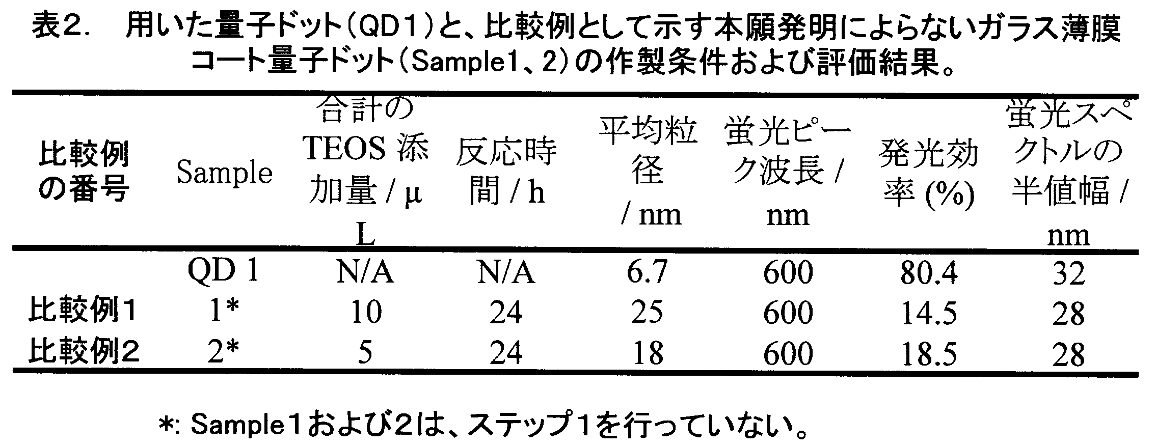
Claims (17)
- Cd及びSeを含む量子ドットが、平均膜厚3nm以下のシリコンアルコキシドからなるシリカガラスを含む薄膜でコートされてなる蛍光性微粒子。
- 前記量子ドットが、Cd及びSeを含むコアと、Zn及びSを含むシェルとからなる請求項1に記載の蛍光性微粒子。
- 前記量子ドットの発光ピーク波長が650nm以上1000nm以下である、請求項2に記載の蛍光性微粒子。
- 前記量子ドットが、シリコンアルコキシドからなるシリカガラスで直接にコートされている、請求項1~3のいずれかに記載の蛍光性微粒子。
- 前記量子ドットが疎水性である、請求項1~4のいずれかに記載の蛍光性微粒子。
- 前記量子ドットの蛍光スペクトルの半値全幅が35nm以下である、請求項1~5のいずれかに記載の蛍光性微粒子。
- 平均粒径が15nm以下である、請求項1~6のいずれかに記載の蛍光性微粒子。
- 表面にCOOH基、NH2基、SH基及びこれらの塩、並びにポリエチレングリコール由来の基よりなる群から選ばれる少なくとも1種類を有する、請求項1~7のいずれかに記載の蛍光性微粒子。
- 量子ドットの数が1個である、請求項1~8のいずれかに記載の蛍光性微粒子。
- 発光効率が20%以上である、請求項1~9のいずれかに記載の蛍光性微粒子。
- 蛍光試薬用である請求項1~10のいずれかに記載の蛍光性微粒子。
- 電子材料用である請求項1~10のいずれかに記載の蛍光性微粒子。
- エレクトロルミネッセンス及び/又はカソードルミネッセンスを示す、請求項1~10のいずれかに記載の蛍光性微粒子。
- (1)Cd及びSeを含む量子ドット及びシリコンアルコキシドを含有する疎水性溶媒を1時間以上攪拌して疎水性量子ドットを作製する工程
を備える、請求項1~13のいずれかに記載の蛍光性微粒子の製造方法。 - さらに、
(2)作製した疎水性量子ドットを、親水性に転換する工程
を備える、請求項14に記載の蛍光性微粒子の製造方法。 - 前記工程(2)が、作製した疎水性量子ドット、アルカリ性水溶液及びシリコンアルコキシドを、逆ミセル溶液に添加して1時間以上攪拌する工程である、請求項15に記載の蛍光性微粒子の製造方法。
- 前記Cd及びSeを含む量子ドットが、溶液に含まれるCdの量をXミリモル、加えるSeのスピードをYミリモル/分としたときに、0.3X<Y<2Xの条件を含む工程で作製されたものである請求項14~16のいずれかに記載の蛍光性微粒子の製造方法。
Priority Applications (1)
| Application Number | Priority Date | Filing Date | Title |
|---|---|---|---|
| JP2013516320A JP5709188B2 (ja) | 2011-05-23 | 2012-05-17 | 薄膜シリカガラスコート量子ドットからなる蛍光性微粒子及びその製造方法 |
Applications Claiming Priority (2)
| Application Number | Priority Date | Filing Date | Title |
|---|---|---|---|
| JP2011114627 | 2011-05-23 | ||
| JP2011-114627 | 2011-05-23 |
Publications (1)
| Publication Number | Publication Date |
|---|---|
| WO2012161065A1 true WO2012161065A1 (ja) | 2012-11-29 |
Family
ID=47217143
Family Applications (1)
| Application Number | Title | Priority Date | Filing Date |
|---|---|---|---|
| PCT/JP2012/062589 Ceased WO2012161065A1 (ja) | 2011-05-23 | 2012-05-17 | 薄膜シリカガラスコート量子ドットからなる蛍光性微粒子及びその製造方法 |
Country Status (2)
| Country | Link |
|---|---|
| JP (1) | JP5709188B2 (ja) |
| WO (1) | WO2012161065A1 (ja) |
Cited By (21)
| Publication number | Priority date | Publication date | Assignee | Title |
|---|---|---|---|---|
| JP2015062872A (ja) * | 2013-09-25 | 2015-04-09 | 株式会社日本触媒 | 固体微粒子の製造方法 |
| WO2015156226A1 (ja) * | 2014-04-08 | 2015-10-15 | Nsマテリアルズ株式会社 | 量子ドット及びその製造方法、並びに、前記量子ドットを用いた成形体、シート部材、波長変換部材、発光装置 |
| JP2016173888A (ja) * | 2015-03-16 | 2016-09-29 | 日本放送協会 | 発光素子及びその製造方法、並びに表示装置 |
| JP2017044672A (ja) * | 2015-08-28 | 2017-03-02 | 国立研究開発法人産業技術総合研究所 | ナノ粒子のスクリーニング方法及びスクリーニングシステム |
| WO2017038511A1 (ja) * | 2015-08-28 | 2017-03-09 | 国立研究開発法人産業技術総合研究所 | ナノ粒子のスクリーニング方法及びスクリーニングシステム、並びに、ナノ粒子及びその製造方法 |
| WO2017085831A1 (ja) * | 2015-11-19 | 2017-05-26 | コニカミノルタ株式会社 | 発光体及びその製造方法 |
| JP2017160072A (ja) * | 2016-03-09 | 2017-09-14 | 三菱マテリアル株式会社 | CdSeコロイド粒子の製造方法 |
| JP2017160073A (ja) * | 2016-03-09 | 2017-09-14 | 三菱マテリアル株式会社 | CdSeコロイド粒子の製造方法 |
| KR20190084869A (ko) | 2016-11-17 | 2019-07-17 | 니폰 덴키 가라스 가부시키가이샤 | 무기 나노 형광체 입자 복합체 및 파장 변환 부재 |
| JP2020526596A (ja) * | 2017-07-17 | 2020-08-31 | 京東方科技集團股▲ふん▼有限公司Boe Technology Group Co.,Ltd. | リガンド修飾された量子ドット組成物、リガンド修飾された量子ドット層及びそれらの作製方法、量子ドット発光ダイオード |
| US10954440B2 (en) | 2018-03-09 | 2021-03-23 | Samsung Electronics Co., Ltd. | Quantum dots and devices including the same |
| US10954441B2 (en) | 2018-03-09 | 2021-03-23 | Samsung Electronics Co., Ltd. | Quantum dots |
| US11011720B2 (en) | 2018-03-09 | 2021-05-18 | Samsung Electronics Co., Ltd. | Semiconductor nanocrystal particles, production methods thereof, and devices including the same |
| CN113975410A (zh) * | 2021-10-21 | 2022-01-28 | 浙江中医药大学 | 一种荧光靶向纳米药物载体和靶向药物及其制备方法 |
| JP2022074714A (ja) * | 2020-11-05 | 2022-05-18 | 国立研究開発法人産業技術総合研究所 | 蛍光性微粒子及びその製造方法、該蛍光性微粒子を用いたディスプレイ、生体物の蛍光標識又は蛍光試薬 |
| US11655415B2 (en) | 2017-06-19 | 2023-05-23 | Nippon Electric Glass Co., Ltd. | Nanophosphor-attached inorganic particles and wavelength conversion member |
| CN116355608A (zh) * | 2021-12-28 | 2023-06-30 | 财团法人工业技术研究院 | 光转换材料及其制备方法 |
| CN116515489A (zh) * | 2023-04-18 | 2023-08-01 | 浙江工业大学 | 一种用于对醇中痕量水颜色识别可视化快速检测的双色比率荧光探针及其应用 |
| WO2024214668A1 (ja) * | 2023-04-14 | 2024-10-17 | 株式会社 量子材料技術 | 蛍光性ガラス微粒子、及び、それを備える蛍光体、蛍光機能材の中間生成物、蛍光機能材の最終生成物 |
| WO2025215792A1 (ja) * | 2024-04-11 | 2025-10-16 | シャープディスプレイテクノロジー株式会社 | 発光素子、表示装置、発光素子の製造方法 |
| US12509631B2 (en) | 2017-05-11 | 2025-12-30 | Samsung Electronics Co., Ltd. | Semiconductor nanocrystal particles and devices including the same |
Citations (3)
| Publication number | Priority date | Publication date | Assignee | Title |
|---|---|---|---|---|
| JP2005105244A (ja) * | 2003-01-24 | 2005-04-21 | National Institute Of Advanced Industrial & Technology | 半導体超微粒子及び蛍光体 |
| WO2007034877A1 (ja) * | 2005-09-22 | 2007-03-29 | National Institute Of Advanced Industrial Science And Technology | 半導体ナノ粒子分散ガラス微粒子及びその作製方法 |
| WO2009028282A1 (ja) * | 2007-08-28 | 2009-03-05 | National Institute Of Advanced Industrial Science And Technology | 新規ナノ粒子発光体 |
-
2012
- 2012-05-17 WO PCT/JP2012/062589 patent/WO2012161065A1/ja not_active Ceased
- 2012-05-17 JP JP2013516320A patent/JP5709188B2/ja not_active Expired - Fee Related
Patent Citations (3)
| Publication number | Priority date | Publication date | Assignee | Title |
|---|---|---|---|---|
| JP2005105244A (ja) * | 2003-01-24 | 2005-04-21 | National Institute Of Advanced Industrial & Technology | 半導体超微粒子及び蛍光体 |
| WO2007034877A1 (ja) * | 2005-09-22 | 2007-03-29 | National Institute Of Advanced Industrial Science And Technology | 半導体ナノ粒子分散ガラス微粒子及びその作製方法 |
| WO2009028282A1 (ja) * | 2007-08-28 | 2009-03-05 | National Institute Of Advanced Industrial Science And Technology | 新規ナノ粒子発光体 |
Cited By (35)
| Publication number | Priority date | Publication date | Assignee | Title |
|---|---|---|---|---|
| JP2015062872A (ja) * | 2013-09-25 | 2015-04-09 | 株式会社日本触媒 | 固体微粒子の製造方法 |
| WO2015156226A1 (ja) * | 2014-04-08 | 2015-10-15 | Nsマテリアルズ株式会社 | 量子ドット及びその製造方法、並びに、前記量子ドットを用いた成形体、シート部材、波長変換部材、発光装置 |
| US10815425B2 (en) | 2014-04-08 | 2020-10-27 | Ns Materials Inc. | Quantum dot, manufacturing method of the dot, and compact, sheet member, wavelength conversion member and light emitting apparatus using the quantum dot |
| US10266769B2 (en) | 2014-04-08 | 2019-04-23 | Ns Materials Inc. | Quantum dot, manufacturing method of the dot, and compact, sheet member, wavelength conversion member and light emitting apparatus using the quantum dot |
| JPWO2015156226A1 (ja) * | 2014-04-08 | 2017-04-13 | Nsマテリアルズ株式会社 | 量子ドット及びその製造方法、並びに、前記量子ドットを用いた成形体、シート部材、波長変換部材、発光装置 |
| US10676667B2 (en) | 2014-04-08 | 2020-06-09 | Ns Materials Inc. | Quantum dot, manufacturing method of the dot, and compact, sheet member, wavelength conversion member and light emitting apparatus using the quantum dot |
| JP2016173888A (ja) * | 2015-03-16 | 2016-09-29 | 日本放送協会 | 発光素子及びその製造方法、並びに表示装置 |
| CN108291872A (zh) * | 2015-08-28 | 2018-07-17 | 国立研究开发法人产业技术综合研究所 | 纳米粒子的筛选方法及筛选系统、与纳米粒子及其制造方法 |
| US10948412B2 (en) | 2015-08-28 | 2021-03-16 | National Institute Of Advanced Industrial Science And Technology | Method and system for screening nanoparticle, and nanoparticle and method of producing the same |
| US20190025211A1 (en) * | 2015-08-28 | 2019-01-24 | National Institute Of Advanced Industrial Science And Technology | Method and system for screening nanoparticle, and nanoparticle and method of producing the same |
| WO2017038511A1 (ja) * | 2015-08-28 | 2017-03-09 | 国立研究開発法人産業技術総合研究所 | ナノ粒子のスクリーニング方法及びスクリーニングシステム、並びに、ナノ粒子及びその製造方法 |
| JP2017044672A (ja) * | 2015-08-28 | 2017-03-02 | 国立研究開発法人産業技術総合研究所 | ナノ粒子のスクリーニング方法及びスクリーニングシステム |
| WO2017085831A1 (ja) * | 2015-11-19 | 2017-05-26 | コニカミノルタ株式会社 | 発光体及びその製造方法 |
| JP2017160073A (ja) * | 2016-03-09 | 2017-09-14 | 三菱マテリアル株式会社 | CdSeコロイド粒子の製造方法 |
| JP2017160072A (ja) * | 2016-03-09 | 2017-09-14 | 三菱マテリアル株式会社 | CdSeコロイド粒子の製造方法 |
| KR20190084869A (ko) | 2016-11-17 | 2019-07-17 | 니폰 덴키 가라스 가부시키가이샤 | 무기 나노 형광체 입자 복합체 및 파장 변환 부재 |
| US11584887B2 (en) | 2016-11-17 | 2023-02-21 | Nippon Electric Glass Co., Ltd. | Inorganic nano fluorescent particle composite and wavelength converting member |
| US12509631B2 (en) | 2017-05-11 | 2025-12-30 | Samsung Electronics Co., Ltd. | Semiconductor nanocrystal particles and devices including the same |
| US11655415B2 (en) | 2017-06-19 | 2023-05-23 | Nippon Electric Glass Co., Ltd. | Nanophosphor-attached inorganic particles and wavelength conversion member |
| US11453820B2 (en) | 2017-07-17 | 2022-09-27 | Beijing Boe Technology Development Co., Ltd. | Ligand-modified quantum dot composition, ligand-modified quantum dot layer, preparation methods thereof, quantum dot light emitting diode |
| JP2020526596A (ja) * | 2017-07-17 | 2020-08-31 | 京東方科技集團股▲ふん▼有限公司Boe Technology Group Co.,Ltd. | リガンド修飾された量子ドット組成物、リガンド修飾された量子ドット層及びそれらの作製方法、量子ドット発光ダイオード |
| JP7190907B2 (ja) | 2017-07-17 | 2022-12-16 | 京東方科技集團股▲ふん▼有限公司 | リガンド修飾された量子ドット組成物、リガンド修飾された量子ドット層及びそれらの作製方法、量子ドット発光ダイオード |
| US11011720B2 (en) | 2018-03-09 | 2021-05-18 | Samsung Electronics Co., Ltd. | Semiconductor nanocrystal particles, production methods thereof, and devices including the same |
| US11591518B2 (en) | 2018-03-09 | 2023-02-28 | Samsung Electronics Co., Ltd. | Quantum dots and devices including the same |
| US10954441B2 (en) | 2018-03-09 | 2021-03-23 | Samsung Electronics Co., Ltd. | Quantum dots |
| US11981852B2 (en) | 2018-03-09 | 2024-05-14 | Samsung Electronics Co., Ltd. | Quantum dots and devices including the same |
| US12338380B2 (en) | 2018-03-09 | 2025-06-24 | Samsung Electronics Co., Ltd. | Quantum dots and devices including the same |
| US10954440B2 (en) | 2018-03-09 | 2021-03-23 | Samsung Electronics Co., Ltd. | Quantum dots and devices including the same |
| JP2022074714A (ja) * | 2020-11-05 | 2022-05-18 | 国立研究開発法人産業技術総合研究所 | 蛍光性微粒子及びその製造方法、該蛍光性微粒子を用いたディスプレイ、生体物の蛍光標識又は蛍光試薬 |
| CN113975410A (zh) * | 2021-10-21 | 2022-01-28 | 浙江中医药大学 | 一种荧光靶向纳米药物载体和靶向药物及其制备方法 |
| CN116355608A (zh) * | 2021-12-28 | 2023-06-30 | 财团法人工业技术研究院 | 光转换材料及其制备方法 |
| WO2024214668A1 (ja) * | 2023-04-14 | 2024-10-17 | 株式会社 量子材料技術 | 蛍光性ガラス微粒子、及び、それを備える蛍光体、蛍光機能材の中間生成物、蛍光機能材の最終生成物 |
| CN116515489A (zh) * | 2023-04-18 | 2023-08-01 | 浙江工业大学 | 一种用于对醇中痕量水颜色识别可视化快速检测的双色比率荧光探针及其应用 |
| CN116515489B (zh) * | 2023-04-18 | 2024-04-26 | 浙江工业大学 | 一种用于对醇中痕量水颜色识别可视化快速检测的双色比率荧光探针及其应用 |
| WO2025215792A1 (ja) * | 2024-04-11 | 2025-10-16 | シャープディスプレイテクノロジー株式会社 | 発光素子、表示装置、発光素子の製造方法 |
Also Published As
| Publication number | Publication date |
|---|---|
| JP5709188B2 (ja) | 2015-04-30 |
| JPWO2012161065A1 (ja) | 2014-07-31 |
Similar Documents
| Publication | Publication Date | Title |
|---|---|---|
| JP5709188B2 (ja) | 薄膜シリカガラスコート量子ドットからなる蛍光性微粒子及びその製造方法 | |
| JP5682069B2 (ja) | ゾル−ゲル法によって作製した半導体ナノ粒子分散蛍光性微粒子 | |
| KR101651798B1 (ko) | 양자점 함유 입자 및 이의 제조 방법 | |
| JP5907544B2 (ja) | ナノ粒子の製造方法 | |
| Wu et al. | Synthesis of highly stable CuInZnS/ZnS//ZnS quantum dots with thick shell and its application to quantitative immunoassay | |
| JP5551435B2 (ja) | ナノ結晶でドープしたマトリックス | |
| JP4245182B2 (ja) | 水溶性蛍光材料およびその製造方法 | |
| KR101567327B1 (ko) | 양자점 함유 복합입자 및 이의 제조 방법 | |
| CN107916448A (zh) | 使用有机配体的混合物制备纳米晶体 | |
| CN110072969A (zh) | 半导体发光纳米粒子 | |
| KR101575396B1 (ko) | 양자점 함유 나노복합입자 및 그 제조방법 | |
| US20100252778A1 (en) | Novel nanoparticle phosphor | |
| WO2007034877A1 (ja) | 半導体ナノ粒子分散ガラス微粒子及びその作製方法 | |
| JP2015127362A (ja) | 発光体粒子、発光体粒子の製造方法、発光体粒子を用いた光学フィルムおよび光学デバイス | |
| JP7269591B1 (ja) | AgAuS系多元化合物からなる半導体ナノ粒子 | |
| JP2017110039A (ja) | 発光体及びその製造方法、発光体を用いた蛍光プローブ、蛍光プローブ分散液、led装置、投射型表示装置用カラーホイール、波長変換フィルム、ディスプレイ装置、並びに光電変換装置 | |
| Goryacheva et al. | Influence of particle architecture on the photoluminescence properties of silica-coated CdSe core/shell quantum dots | |
| JP2022074714A (ja) | 蛍光性微粒子及びその製造方法、該蛍光性微粒子を用いたディスプレイ、生体物の蛍光標識又は蛍光試薬 | |
| JP2017122175A (ja) | 半導体ナノ粒子及びその製造方法、並びに半導体ナノ粒子を用いた蛍光プローブ、led装置、波長変換フィルム、及び光電変換装置 | |
| JP2017110040A (ja) | コア/シェル型ナノ粒子の製造方法、及び発光体 | |
| US20100038626A1 (en) | Semiconductor nanoparticle aggregate, method for producing the same, and biological substance labeling agent utilizing the same | |
| JPWO2012026149A1 (ja) | 半導体ナノ粒子集積体 | |
| Chung et al. | Performance changes of surface coated red phosphors with silica nanoparticles and silica nanocomposites | |
| JP2013204004A (ja) | 高輝度半導体ナノ粒子集積体 | |
| JPWO2009011194A1 (ja) | 半導体ナノ粒子蛍光体の集合体、その製造方法、及びそれを用いた単一分子観察方法 |
Legal Events
| Date | Code | Title | Description |
|---|---|---|---|
| 121 | Ep: the epo has been informed by wipo that ep was designated in this application |
Ref document number: 12790173 Country of ref document: EP Kind code of ref document: A1 |
|
| ENP | Entry into the national phase |
Ref document number: 2013516320 Country of ref document: JP Kind code of ref document: A |
|
| NENP | Non-entry into the national phase |
Ref country code: DE |
|
| 122 | Ep: pct application non-entry in european phase |
Ref document number: 12790173 Country of ref document: EP Kind code of ref document: A1 |