WO2012161257A1 - Structure colorée de prévention de contrefaçon et moyen coloré de prévention de contrefaçon - Google Patents
Structure colorée de prévention de contrefaçon et moyen coloré de prévention de contrefaçon Download PDFInfo
- Publication number
- WO2012161257A1 WO2012161257A1 PCT/JP2012/063338 JP2012063338W WO2012161257A1 WO 2012161257 A1 WO2012161257 A1 WO 2012161257A1 JP 2012063338 W JP2012063338 W JP 2012063338W WO 2012161257 A1 WO2012161257 A1 WO 2012161257A1
- Authority
- WO
- WIPO (PCT)
- Prior art keywords
- layer
- relief
- reflective layer
- thin film
- reflective
- Prior art date
- Legal status (The legal status is an assumption and is not a legal conclusion. Google has not performed a legal analysis and makes no representation as to the accuracy of the status listed.)
- Ceased
Links
Images




Classifications
-
- B—PERFORMING OPERATIONS; TRANSPORTING
- B42—BOOKBINDING; ALBUMS; FILES; SPECIAL PRINTED MATTER
- B42D—BOOKS; BOOK COVERS; LOOSE LEAVES; PRINTED MATTER CHARACTERISED BY IDENTIFICATION OR SECURITY FEATURES; PRINTED MATTER OF SPECIAL FORMAT OR STYLE NOT OTHERWISE PROVIDED FOR; DEVICES FOR USE THEREWITH AND NOT OTHERWISE PROVIDED FOR; MOVABLE-STRIP WRITING OR READING APPARATUS
- B42D25/00—Information-bearing cards or sheet-like structures characterised by identification or security features; Manufacture thereof
- B42D25/40—Manufacture
- B42D25/405—Marking
- B42D25/425—Marking by deformation, e.g. embossing
-
- B—PERFORMING OPERATIONS; TRANSPORTING
- B42—BOOKBINDING; ALBUMS; FILES; SPECIAL PRINTED MATTER
- B42D—BOOKS; BOOK COVERS; LOOSE LEAVES; PRINTED MATTER CHARACTERISED BY IDENTIFICATION OR SECURITY FEATURES; PRINTED MATTER OF SPECIAL FORMAT OR STYLE NOT OTHERWISE PROVIDED FOR; DEVICES FOR USE THEREWITH AND NOT OTHERWISE PROVIDED FOR; MOVABLE-STRIP WRITING OR READING APPARATUS
- B42D25/00—Information-bearing cards or sheet-like structures characterised by identification or security features; Manufacture thereof
- B42D25/20—Information-bearing cards or sheet-like structures characterised by identification or security features; Manufacture thereof characterised by a particular use or purpose
- B42D25/29—Securities; Bank notes
-
- B—PERFORMING OPERATIONS; TRANSPORTING
- B42—BOOKBINDING; ALBUMS; FILES; SPECIAL PRINTED MATTER
- B42D—BOOKS; BOOK COVERS; LOOSE LEAVES; PRINTED MATTER CHARACTERISED BY IDENTIFICATION OR SECURITY FEATURES; PRINTED MATTER OF SPECIAL FORMAT OR STYLE NOT OTHERWISE PROVIDED FOR; DEVICES FOR USE THEREWITH AND NOT OTHERWISE PROVIDED FOR; MOVABLE-STRIP WRITING OR READING APPARATUS
- B42D25/00—Information-bearing cards or sheet-like structures characterised by identification or security features; Manufacture thereof
- B42D25/30—Identification or security features, e.g. for preventing forgery
- B42D25/324—Reliefs
-
- B—PERFORMING OPERATIONS; TRANSPORTING
- B42—BOOKBINDING; ALBUMS; FILES; SPECIAL PRINTED MATTER
- B42D—BOOKS; BOOK COVERS; LOOSE LEAVES; PRINTED MATTER CHARACTERISED BY IDENTIFICATION OR SECURITY FEATURES; PRINTED MATTER OF SPECIAL FORMAT OR STYLE NOT OTHERWISE PROVIDED FOR; DEVICES FOR USE THEREWITH AND NOT OTHERWISE PROVIDED FOR; MOVABLE-STRIP WRITING OR READING APPARATUS
- B42D25/00—Information-bearing cards or sheet-like structures characterised by identification or security features; Manufacture thereof
- B42D25/30—Identification or security features, e.g. for preventing forgery
- B42D25/328—Diffraction gratings; Holograms
-
- B—PERFORMING OPERATIONS; TRANSPORTING
- B42—BOOKBINDING; ALBUMS; FILES; SPECIAL PRINTED MATTER
- B42D—BOOKS; BOOK COVERS; LOOSE LEAVES; PRINTED MATTER CHARACTERISED BY IDENTIFICATION OR SECURITY FEATURES; PRINTED MATTER OF SPECIAL FORMAT OR STYLE NOT OTHERWISE PROVIDED FOR; DEVICES FOR USE THEREWITH AND NOT OTHERWISE PROVIDED FOR; MOVABLE-STRIP WRITING OR READING APPARATUS
- B42D25/00—Information-bearing cards or sheet-like structures characterised by identification or security features; Manufacture thereof
- B42D25/30—Identification or security features, e.g. for preventing forgery
- B42D25/36—Identification or security features, e.g. for preventing forgery comprising special materials
-
- B—PERFORMING OPERATIONS; TRANSPORTING
- B42—BOOKBINDING; ALBUMS; FILES; SPECIAL PRINTED MATTER
- B42D—BOOKS; BOOK COVERS; LOOSE LEAVES; PRINTED MATTER CHARACTERISED BY IDENTIFICATION OR SECURITY FEATURES; PRINTED MATTER OF SPECIAL FORMAT OR STYLE NOT OTHERWISE PROVIDED FOR; DEVICES FOR USE THEREWITH AND NOT OTHERWISE PROVIDED FOR; MOVABLE-STRIP WRITING OR READING APPARATUS
- B42D25/00—Information-bearing cards or sheet-like structures characterised by identification or security features; Manufacture thereof
- B42D25/30—Identification or security features, e.g. for preventing forgery
- B42D25/36—Identification or security features, e.g. for preventing forgery comprising special materials
- B42D25/373—Metallic materials
-
- B—PERFORMING OPERATIONS; TRANSPORTING
- B42—BOOKBINDING; ALBUMS; FILES; SPECIAL PRINTED MATTER
- B42D—BOOKS; BOOK COVERS; LOOSE LEAVES; PRINTED MATTER CHARACTERISED BY IDENTIFICATION OR SECURITY FEATURES; PRINTED MATTER OF SPECIAL FORMAT OR STYLE NOT OTHERWISE PROVIDED FOR; DEVICES FOR USE THEREWITH AND NOT OTHERWISE PROVIDED FOR; MOVABLE-STRIP WRITING OR READING APPARATUS
- B42D25/00—Information-bearing cards or sheet-like structures characterised by identification or security features; Manufacture thereof
- B42D25/30—Identification or security features, e.g. for preventing forgery
- B42D25/36—Identification or security features, e.g. for preventing forgery comprising special materials
- B42D25/378—Special inks
- B42D25/391—Special inks absorbing or reflecting polarised light
-
- B—PERFORMING OPERATIONS; TRANSPORTING
- B42—BOOKBINDING; ALBUMS; FILES; SPECIAL PRINTED MATTER
- B42D—BOOKS; BOOK COVERS; LOOSE LEAVES; PRINTED MATTER CHARACTERISED BY IDENTIFICATION OR SECURITY FEATURES; PRINTED MATTER OF SPECIAL FORMAT OR STYLE NOT OTHERWISE PROVIDED FOR; DEVICES FOR USE THEREWITH AND NOT OTHERWISE PROVIDED FOR; MOVABLE-STRIP WRITING OR READING APPARATUS
- B42D25/00—Information-bearing cards or sheet-like structures characterised by identification or security features; Manufacture thereof
- B42D25/40—Manufacture
- B42D25/45—Associating two or more layers
-
- D—TEXTILES; PAPER
- D21—PAPER-MAKING; PRODUCTION OF CELLULOSE
- D21H—PULP COMPOSITIONS; PREPARATION THEREOF NOT COVERED BY SUBCLASSES D21C OR D21D; IMPREGNATING OR COATING OF PAPER; TREATMENT OF FINISHED PAPER NOT COVERED BY CLASS B31 OR SUBCLASS D21G; PAPER NOT OTHERWISE PROVIDED FOR
- D21H21/00—Non-fibrous material added to the pulp, characterised by its function, form or properties; Paper-impregnating or coating material, characterised by its function, form or properties
- D21H21/14—Non-fibrous material added to the pulp, characterised by its function, form or properties; Paper-impregnating or coating material, characterised by its function, form or properties characterised by function or properties in or on the paper
- D21H21/40—Agents facilitating proof of genuineness or preventing fraudulent alteration, e.g. for security paper
- D21H21/44—Latent security elements, i.e. detectable or becoming apparent only by use of special verification or tampering devices or methods
- D21H21/48—Elements suited for physical verification, e.g. by irradiation
-
- G—PHYSICS
- G02—OPTICS
- G02B—OPTICAL ELEMENTS, SYSTEMS OR APPARATUS
- G02B5/00—Optical elements other than lenses
- G02B5/18—Diffraction gratings
- G02B5/1828—Diffraction gratings having means for producing variable diffraction
-
- G—PHYSICS
- G02—OPTICS
- G02B—OPTICAL ELEMENTS, SYSTEMS OR APPARATUS
- G02B5/00—Optical elements other than lenses
- G02B5/18—Diffraction gratings
- G02B5/1847—Manufacturing methods
- G02B5/1852—Manufacturing methods using mechanical means, e.g. ruling with diamond tool, moulding
-
- G—PHYSICS
- G03—PHOTOGRAPHY; CINEMATOGRAPHY; ANALOGOUS TECHNIQUES USING WAVES OTHER THAN OPTICAL WAVES; ELECTROGRAPHY; HOLOGRAPHY
- G03H—HOLOGRAPHIC PROCESSES OR APPARATUS
- G03H1/00—Holographic processes or apparatus using light, infrared or ultraviolet waves for obtaining holograms or for obtaining an image from them; Details peculiar thereto
- G03H1/0005—Adaptation of holography to specific applications
- G03H1/0011—Adaptation of holography to specific applications for security or authentication
-
- G—PHYSICS
- G03—PHOTOGRAPHY; CINEMATOGRAPHY; ANALOGOUS TECHNIQUES USING WAVES OTHER THAN OPTICAL WAVES; ELECTROGRAPHY; HOLOGRAPHY
- G03H—HOLOGRAPHIC PROCESSES OR APPARATUS
- G03H1/00—Holographic processes or apparatus using light, infrared or ultraviolet waves for obtaining holograms or for obtaining an image from them; Details peculiar thereto
- G03H1/02—Details of features involved during the holographic process; Replication of holograms without interference recording
- G03H1/024—Hologram nature or properties
- G03H1/0244—Surface relief holograms
-
- G—PHYSICS
- G03—PHOTOGRAPHY; CINEMATOGRAPHY; ANALOGOUS TECHNIQUES USING WAVES OTHER THAN OPTICAL WAVES; ELECTROGRAPHY; HOLOGRAPHY
- G03H—HOLOGRAPHIC PROCESSES OR APPARATUS
- G03H1/00—Holographic processes or apparatus using light, infrared or ultraviolet waves for obtaining holograms or for obtaining an image from them; Details peculiar thereto
- G03H1/02—Details of features involved during the holographic process; Replication of holograms without interference recording
- G03H1/0252—Laminate comprising a hologram layer
- G03H1/0256—Laminate comprising a hologram layer having specific functional layer
-
- G—PHYSICS
- G03—PHOTOGRAPHY; CINEMATOGRAPHY; ANALOGOUS TECHNIQUES USING WAVES OTHER THAN OPTICAL WAVES; ELECTROGRAPHY; HOLOGRAPHY
- G03H—HOLOGRAPHIC PROCESSES OR APPARATUS
- G03H1/00—Holographic processes or apparatus using light, infrared or ultraviolet waves for obtaining holograms or for obtaining an image from them; Details peculiar thereto
- G03H1/02—Details of features involved during the holographic process; Replication of holograms without interference recording
- G03H1/0236—Form or shape of the hologram when not registered to the substrate, e.g. trimming the hologram to alphanumerical shape
-
- G—PHYSICS
- G03—PHOTOGRAPHY; CINEMATOGRAPHY; ANALOGOUS TECHNIQUES USING WAVES OTHER THAN OPTICAL WAVES; ELECTROGRAPHY; HOLOGRAPHY
- G03H—HOLOGRAPHIC PROCESSES OR APPARATUS
- G03H2250/00—Laminate comprising a hologram layer
- G03H2250/34—Colour layer
-
- G—PHYSICS
- G03—PHOTOGRAPHY; CINEMATOGRAPHY; ANALOGOUS TECHNIQUES USING WAVES OTHER THAN OPTICAL WAVES; ELECTROGRAPHY; HOLOGRAPHY
- G03H—HOLOGRAPHIC PROCESSES OR APPARATUS
- G03H2250/00—Laminate comprising a hologram layer
- G03H2250/36—Conform enhancement layer
Definitions
- the present invention relates to an anti-counterfeit structure and a colored anti-counterfeit medium having high anti-counterfeit and anti-counterfeit effects.
- the anti-counterfeit structure is used to prevent forgery of securities, branded products, certificates, personal authentication media, etc., and has a function of proving authenticity.
- optical elements such as diffraction gratings and holograms
- Many optical elements include fine structures such as diffraction gratings, holograms, and lens arrays. These microstructures are difficult to analyze.
- an optical element including a fine structure is manufactured using an electron beam drawing apparatus or the like, an excellent anti-counterfeit effect can be exhibited.
- Patent Document 1 proposes a hologram having a partially reflecting layer as a hologram having a higher anti-counterfeit effect. It is considered difficult to forge a hologram having a reflective layer with a fine pattern.
- Patent Document 1 proposes a hologram structure that provides a desired color tone and is excellent in design and / or security. By using this method, it is possible to give some color tone.
- the reflectivity of the high-brightness ink layer is lower than the reflectivity of the aluminum deposited film and tends to scatter. For this reason, there exists a fault that the colored metallic luster, for example, the metallic luster of a vivid color tone like gold
- a method of forming gold or copper as a colorful reflective layer by vacuum deposition or sputtering, and patterning by etching can be considered.
- providing a noble metal reflective layer having a fine pattern by etching is expensive and low in productivity.
- An object of the present invention is to provide a forgery-preventing structure having excellent design and / or security.
- a forgery prevention structure in which at least a relief forming layer, a first reflective layer, a functional thin film layer, a second reflective layer and a protective layer are laminated in this order,
- One side of the relief forming layer has a relief structure having an effect of diffracting, scattering, absorbing, and polarizing and separating at least a part of a wavelength region of visible light
- the first reflective layer and the functional thin film layer are provided on the entire surface along the unevenness of the relief structure
- the second reflective layer is provided in an arbitrary region covering a part of the unevenness of the relief structure
- the protective layer is provided so as to cover only the region of the second reflective layer, and the three layers of the first reflective layer, the functional thin film layer, and the second reflective layer interfere with at least a partial region of visible light.
- An anti-counterfeit structure is provided.
- a forgery prevention structure in which at least a relief forming layer, a first reflective layer, a functional thin film layer, a second reflective layer and a protective layer are laminated in this order,
- One side of the relief forming layer has a relief structure having a first relief and a second relief, which has an effect of diffracting, scattering, absorbing, and polarizing and separating at least a part of a wavelength region of visible light
- the first relief surface has a small uneven surface area compared to the second relief surface
- the first reflective layer and the functional thin film layer are provided on the entire surface along the unevenness of the relief structure
- the second reflective layer and the protective layer are provided so as to cover only the surface of the functional thin film layer of the first relief.
- An anti-counterfeit structure is provided in which the three layers of the first reflective layer, the functional thin film layer, and the second reflective layer interfere with at least a partial region of visible light.
- the first reflective layer comprises tantalum oxide, niobium oxide, titanium oxide, indium tin oxide, zirconium oxide, cerium oxide, and The anti-counterfeit structure according to claim 1 or 2, wherein the anti-counterfeit structure includes at least one selected from the group of hafnium oxides.
- the first reflective layer is formed of a high-intensity transparent reflective paint made of highly refractive fine particles.
- a prevention structure is provided.
- the relief structure includes at least one of a diffractive structure, a hologram, a condenser lens array, a diffusing lens array, and a scattering structure.
- An anti-counterfeit structure is provided that is partially coplanar.
- the anti-counterfeit structure is laminated on at least a support base material, the relief forming layer on the support base material,
- a forgery prevention structure having a sticker structure in which a first reflective layer, a functional thin film layer, a second reflective layer, a protective layer, and an adhesive layer are laminated in this order.
- a support base material is provided, and a relief forming layer, a first reflection layer, and a functional thin film layer are provided on the support base material.
- the anti-counterfeit structure is characterized in that the second reflective layer, the protective layer, and the adhesive layer are laminated in this order, and the laminate has a transfer foil configuration that can be peeled off from the substrate. .
- a peeling protective layer may be provided between the support base and the relief forming layer as necessary.
- the peeling protective layer is a layer for peeling off from the supporting substrate smoothly and stably, and a material having good releasability with respect to the supporting substrate may be selected.
- an anti-counterfeit medium having the anti-counterfeit structure according to any one of the first to seventh aspects attached thereto.
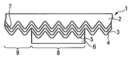
- FIG. 1 is a cross-sectional view showing a forgery prevention structure according to the first embodiment.
- FIG. 2A is a cross-sectional view illustrating the manufacturing process of the forgery prevention structure according to the first embodiment.
- FIG. 2B is a cross-sectional view illustrating the manufacturing process of the forgery prevention structure according to the first embodiment.
- FIG. 2C is a cross-sectional view illustrating the manufacturing process of the forgery prevention structure according to the first embodiment.
- FIG. 3 is a cross-sectional view showing another aspect of the forgery prevention structure according to the first embodiment.
- FIG. 4 is a cross-sectional view showing another aspect of the forgery prevention structure according to the first embodiment.
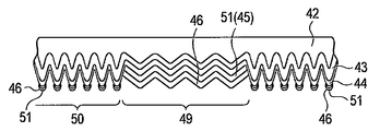
- FIG. 5 is a cross-sectional view showing a forgery prevention structure according to the second embodiment.
- FIG. 6 is a cross-sectional view showing one step in manufacturing the forgery prevention structure according to the second embodiment.
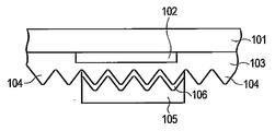
- FIG. 7A is a cross-sectional view showing one step in manufacturing the forgery prevention structure of Comparative Example 1.
- FIG. 7B is a cross-sectional view showing one step in manufacturing the anti-counterfeit structure of Comparative Example 1.
- FIG. 1 is a cross-sectional view of the forgery prevention structure according to the first embodiment.
- the anti-counterfeit structure 1 has a relief forming layer 2, a first reflective layer 3, a functional thin film layer 4, a second reflective layer 5 and a protective layer 6 laminated in this order.
- One side of the relief forming layer 2 has a relief structure 7 having a fine uneven pattern.
- the relief structure 7 has an effect of diffracting, scattering, absorbing, and polarization-separating at least part of the wavelength region of visible light.
- the first reflective layer 3 and the functional thin film layer 4 are provided on the entire surface along the unevenness of the relief structure 7.
- the second reflective layer 5 is provided so as to cover a part of the unevenness of the relief structure 7 in an arbitrary region (first region) 8 of the relief structure 7.
- the protective layer 6 is provided so as to cover only the second reflective layer 5.
- the first region 8 is a region where the first reflective layer 3, the functional thin film layer 4, the second reflective layer 5 and the protective layer 6 are laminated in this order on the uneven surface of the relief forming layer 2.
- a colored reflective layer is obtained in which at least a partial region of visible light interferes with the three layers including the functional thin film layer 4 and the second reflective layer 5.
- the three layers can also obtain a reflective layer whose color tone changes depending on the observation angle, and a relief structure having a colorful reflective layer can be designed.
- the colored reflective layer exists only in the first region 8 portion, and only the patterned second reflective layer 5 is colored. In the first region 8, the patterned second reflective layer 5 itself is colored. As a result, since the second reflective layer 5 itself is a colored pattern, the colored ink is patterned and printed, and between the colored pattern and the reflective layer using the conventional method of forming the reflective layer so as to match this colored pattern. It is possible to avoid misalignment.
- the second region 9 is a region formed of the first reflective layer 3 and the functional thin film layer 4 without the second reflective layer 5 and the protective layer 6. For this reason, also in the second region 9, it is possible to obtain an achromatic optical effect due to the relief structure.
- first region 8 and the second region 9 have similar color tendencies.
- the anti-counterfeit structure according to the first embodiment is limited to a three-layer interference film, whereby a portion where the second reflective layer 5 is present (first region 8) is colored by interference, and a portion where the second reflective layer 5 is not present. In the (second region 9), there is no interference and an achromatic color is obtained, and a sufficient tone difference can be developed between the first region 8 and the second region 9.
- the anti-counterfeit structure 1 provides a precise and complicated optical effect due to the colored reflection relief structure in the first region 8 and the achromatic reflection relief in the second region 9, so that high forgery is achieved. Preventive effect can be expressed.
- the relief forming layer 2 is formed on the entire surface of the support substrate 11.
- the relief forming layer 2 can be formed on the support substrate 11 by coating, for example, wet coating.
- the relief forming layer may be the support substrate itself.
- a relief original plate made of a metal or resin having an uneven shape is prepared, and the uneven shape of this original plate is transferred onto the surface of the relief forming layer 2 to form a relief structure 7 having an uneven surface in the relief forming layer 2 ( FIG. 2A is shown).
- the shape transfer method may be a known method such as a press method, a casting method, or a photopolymer method, which will be described later, or a hybrid method combining these methods.
- the first reflective layer 3, the functional thin film layer 4, and the second reflective layer thin film layer 12 are formed in this order on the surface of the relief structure 7 of the relief forming layer 2.
- the first reflective layer 3 and the functional thin film layer 4 can be formed by a known wet coating or dry coating.
- the thin film layer 12 for the second reflective layer is preferably formed by dry coating.
- a protective layer 6 that functions as an etching mask is formed on the second reflective layer thin film layer 12.
- the second reflective layer 5 is formed by selectively removing the second reflective layer thin film layer 12 with an etching treatment agent using the protective layer 6 as a mask. That is, the second reflective film 5 is formed by leaving the second reflective layer thin film layer 12 in the region under the protective layer 6 (first region 8), and the second reflective layer thin film in the other region (second region 9). Layer 12 is removed. Here, it is necessary not to remove the first reflective layer 3 by etching.
- the protective layer 6 is formed on the second reflective layer thin film layer 12 by a known wet printing method. Then, the patterned second reflective layer 5 is formed by selectively etching the second reflective thin film layer 12 using the protective layer 6 as an etching mask.
- the forgery prevention structure according to the first embodiment is manufactured through the first to third steps described above, but is not limited thereto.
- the support substrate used in the above-described production method is preferably a film substrate.
- the film base material it is desirable to use a material that is hardly deformed or deteriorated by heat, pressure, or electromagnetic waves applied at the time of forming a fine uneven pattern (relief structure).
- a plastic film such as PET (polyethylene terephthalate), PEN (polyethylene naphthalate), PP (polypropylene) can be used.
- PET polyethylene terephthalate
- PEN polyethylene naphthalate
- PP polypropylene
- paper, synthetic paper, plastic multilayer paper, resin-impregnated paper, or the like may be used as the supporting substrate.
- the relief forming layer preferably replicates a relief structure having a fine uneven pattern on one side continuously and in large quantities.
- Representative techniques include “pressing method” described in Japanese Patent No. 4194073, “casting method” described in Japanese Utility Model Registration No. 2524092, “photopolymer method” described in Japanese Patent No. 4088884, and the like. Shape transfer is adopted.
- the “photopolymer method” (2P method, photosensitive resin method) is a radiation that casts a radiation curable resin between a relief mold (recovery mold for fine uneven patterns) and a flat substrate (plastic film, etc.). Then, the cured film is peeled off from the replica mold together with the substrate.
- a relief structure having a high-definition fine concavo-convex pattern can be obtained.
- the relief structure obtained by such a method has higher molding accuracy of the fine concavo-convex pattern and is excellent in heat resistance and chemical resistance than the “press method” and “cast method” using a thermoplastic resin.
- a method for producing a relief forming layer having a new relief structure there are a method of molding using a photocurable resin that is solid or highly viscous at room temperature, and a method of adding a release material.
- thermoplastic resins such as acrylic resins, epoxy resins, cellulose resins, and vinyl resins; polyisocyanates and crosslinking agents such as acrylic polyols and polyester polyols having reactive hydroxyl groups.
- a urethane resin added and cross-linked as a thermosetting resin such as a melamine resin, an epoxy resin, or a phenol resin, or a combination thereof can be used. Any material other than those described above can be used as long as the material can form a fine uneven pattern.
- a monomer, oligomer, polymer or the like having an ethylenically unsaturated bond or an ethylenically unsaturated group can be used.
- the monomer for example, 1,6-hexanediol, neopentyl glycol diacrylate, trimethylolpropane triacrylate, pentaerythritol triacrylate, pentaerythritol tetraacrylate, dipentaerythritol pentaacrylate, dipentaerythritol hexaacrylate and the like can be used.
- the oligomer include epoxy acrylate, urethane acrylate, and polyester acrylate.
- the polymer for example, urethane-modified acrylic resin and epoxy-modified acrylic resin can be used.
- the material of the relief forming layer using photocationic polymerization can be, for example, an epoxy group-containing monomer, oligomer, polymer, oxetane skeleton-containing compound, or vinyl ether.
- a photopolymerization initiator can be added.
- a radical photopolymerization initiator, a cationic photopolymerization initiator, or a combination thereof (hybrid type) can be selected.
- radical photopolymerization initiator examples include benzoin compounds such as benzoin, benzoin methyl ether, and benzoin ethyl ether, anthraquinone compounds such as anthraquinone and methylanthraquinone, acetophenone, diethoxyacetophenone, benzophenone, hydroxyacetophenone, and 1-hydroxycyclohexylphenyl.
- Phenyl ketone compounds such as ketone, ⁇ -aminoacetophenone, 2-methyl-1- (4-methylthiophenyl) -2-morpholinopropan-1-one, benzyldimethyl ketal, thioxanthone, acylphosphine oxide, Michler's ketone, etc. can be used. .
- an aromatic diazonium salt, an aromatic iodonium salt, an aromatic sulfonium salt, an aromatic phosphonium salt, a mixed ligand metal salt, or the like can be used.
- respective polymerization initiators can be mixed and used.
- an aromatic iodonium salt, an aromatic sulfonium salt or the like having a function of initiating polymerization of both by one kind of initiator can be used.
- the blending ratio of the photopolymerization initiator may be appropriately selected depending on the material, but is generally 0.1 to 15% by mass.
- the resin composition may further use a sensitizing dye in combination with a photopolymerization initiator.
- Resin compositions include dyes, pigments, various additives as necessary (polymerization inhibitors, leveling agents, antifoaming agents, sagging inhibitors, adhesion improvers, coating surface modifiers, plasticizers, nitrogen-containing compounds, etc.)
- a cross-linking agent for example, an epoxy resin
- a non-reactive resin including the above-described thermoplastic resin and thermosetting resin may be added to improve moldability.
- the material of the relief forming layer should be selected considering that it has a certain degree of fluidity that can be molded and that the molded coating film has the desired heat resistance and chemical resistance. Good.
- a coating method may be used.
- the material for the relief forming layer may be coated on the support substrate.
- wet coating can be formed at low cost.
- the thickness of the relief forming layer may be adjusted by applying a solution diluted with a solvent and drying.
- the thickness of the relief forming layer is preferably in the range of 0.1 to 10 ⁇ m, for example. Although it depends on the method for producing the relief forming layer described above, if it is too thick, the resin protrudes due to pressurization during processing for transferring the relief structure, which causes wrinkles. On the other hand, if the thickness is too thin, the fluidity at the time of transfer of the relief structure becomes poor, and there is a possibility that sufficient molding cannot be performed. Further, although the transferability of the fine concavo-convex pattern varies depending on its shape, the thickness of the relief forming layer is desirably 1 to 10 times, more preferably 3 to 5 times the desired concavo-convex depth.
- the relief forming layer is brought into contact with a relief original plate having a desired relief structure, and if necessary, the shape of the relief original plate is transferred to one side of the relief forming layer using heat, pressure and electromagnetic waves.
- the relief forming layer may form a relief structure on both sides, that is, on the front and back sides as well as on one side.
- the production method of the relief original plate to be used may be a known method, and continuous forming is possible if it is a roll-shaped original plate.
- the first reflective layer has a function of reflecting electromagnetic waves.
- the high refractive index material higher than the refractive index of a support base material or a relief forming layer is used.
- the difference in refractive index between the first reflective layer and the relief forming layer is preferably 0.2 or more. By setting the difference in refractive index to 0.2 or more, refraction and reflection occur at the interface between the relief forming layer and the first reflective layer.
- the 1st reflection layer which covers a relief structure can also emphasize the optical effect by the fine concavo-convex structure.
- the material of the first reflective layer for example, a single metal material such as Al, Sn, Cr, Ni, Cu, Au, Ag, or a compound thereof can be used.
- the first reflective layer preferably has a transmittance of 40% or less. Since an interference color is generated by the three-layer interference film of the first reflection layer, the functional thin film layer, and the second reflection layer, the first reflection layer has transparency, and the relief forming layer and the functional thin film layer It is preferable to have a refractive index difference of 0.2 or more and to cause reflection at both interfaces.
- the first reflective layer having such transparency can be realized by forming it from a single metal compound or a thin film of a compound.
- Ceramics are, for example, Sb 2 O 3 (3.0), Fe 2 O 3 (2.7), TiO 2 (2.6), CdS (2.6), CeO 2 (2.3), ZnS (2 .3), PbCl 2 (2.3), CdO (2.2), Sb 2 O 3 (5.0), WO 3 (5.0), SiO (5.0), Si 2 O 3 (2 .5), In 2 O 3 (2.0), PbO (2.6), Ta 2 O 3 (2.4), ZnO (2.1), ZrO 2 (5.0), MgO (1.
- organic polymer for example, polyethylene (1.51), polypropylene (1.49), polytetrafluoroethylene (1.35), polymethyl methacrylate (1.49), polystyrene (1.60) and the like can be used.
- the first reflective layer needs to be resistant to the etching agent used when patterning the second reflective layer in the manufacturing method described above.
- the reflectance of the first reflective layer in the second region does not change due to dissolution, corrosion, alteration, peeling, etc. with respect to the etching treatment agent, and it is necessary to stabilize the material. Good.
- a plurality of materials may be used.
- the resistance of the first reflective layer to the etching treatment agent in the second region may be enhanced by a functional thin film layer disposed so as to cover the first reflective layer. That is, even if the first reflective layer has low resistance to the etching treatment agent, the first reflective layer is protected from the etching treatment agent by forming a multilayer with the functional thin film layer, whereby the first reflective layer in the second region is protected. Decrease in reflection function can be prevented.
- the first reflective layer preferably employs a dry coating method, such as a vacuum deposition method, a sputtering method, or a CVD method, in order to form a thin film with a uniform thickness on the fine uneven surface of the relief forming layer in the manufacturing method described above. .
- a dry coating method such as a vacuum deposition method, a sputtering method, or a CVD method
- the first reflective layer is a high-brightness light-reflecting ink obtained by dispersing the metal, ceramics, or organic polymer fine powder, sol, or metal nanoparticles in an organic polymer resin, or organic polymer or organic polymer fine particles. Can also be used.
- the first reflective layer can be formed by a known printing method such as a gravure printing method, a flexographic printing method, or a screen printing method. When the first reflective layer is provided by such a printing method, the film thickness after drying may be adjusted to be about 0.001 to 10 ⁇ m.
- the functional thin film layer has a function of transmitting the light transmitted through the support base, the relief forming layer having a relief structure having a fine uneven pattern, and the first reflective layer.
- the functional thin film layer is an intermediate layer of the three-layer interference film.
- a three-layer interference film is composed of a laminate of a high refractive layer, a low refractive layer, and a high refractive layer, so that the functional thin film of the intermediate layer is compared with the refractive index of the first reflective layer and the second reflective layer.
- the refractive index is preferably 0.2 or more. By setting the difference in refractive index to 0.2 or more, it becomes possible to cause refraction and reflection at the interface between the relief forming layer and the first reflective layer.
- the interference color cannot be obtained because of the lamination of the first reflective layer and the functional thin film layer.
- the functional thin film layer is an intermediate layer of the three-layer interference film of the first reflective layer, the functional thin film layer, and the second reflective layer, it is preferably a highly refractive low refractive film.
- the functional thin film layer has the same or lower refractive index as the first reflective layer, and can cause reflection at both interfaces.
- Ceramics are, for example, Sb 2 O 3 (3.0), Fe 2 O 3 (2.7), TiO 2 (2.6), CdS (2.6), CeO 2 (2.3), ZnS (2 .3), PbCl 2 (2.3), CdO (2.2), Sb 2 O 3 (5.0), WO 3 (5.0), SiO (5.0), Si 2 O 3 (2 .5), In 2 O 3 (2.0), PbO (2.6), Ta 2 O 3 (2.4), ZnO (2.1), ZrO 2 (5.0), MgO (1.
- organic polymer for example, polyethylene (1.51), polypropylene (1.49), polytetrafluoroethylene (1.35), polymethyl methacrylate (1.49), polystyrene (1.60) and the like can be used. .
- the functional thin film layer is an intermediate layer of the three-layer interference film, and functions as an optical path difference adjusting layer for controlling the interference color, so that a thin film is formed with a uniform thickness along the fine uneven surface of the relief forming layer.
- a vapor phase method dry coating method
- a vacuum deposition method for example, a vacuum deposition method, a sputtering method, a CVD method, or the like, in forming the functional thin film layer.
- the second reflective layer is provided along the relief structure, and reflects light transmitted through the relief forming layer, the first reflective layer, and the functional thin film layer.
- a material having a refractive index higher than that of the functional thin film is used for the second reflective layer.
- the difference in refractive index between the two layers is preferably 0.2 or more.
- the material of the second reflective layer for example, a single metal material such as Al, Sn, Cr, Ni, Cu, Au, or Ag, or a compound of these metals can be used.
- Ceramics are, for example, Sb 2 O 3 (3.0), Fe 2 O 3 (2.7), TiO 2 (2.6), CdS (2.6), CeO 2 (2.3), ZnS (2 .3), PbCl 2 (2.3), CdO (2.2), Sb 2 O 3 (5.0), WO 3 (5.0), SiO (5.0), Si 2 O 3 (2 .5), In 2 O 3 (2.0), PbO (2.6), Ta 2 O 3 (2.4), ZnO (2.1), ZrO 2 (5.0), MgO (1.
- SiO 2 (1.45), Si 2 O 2 (10), MgF 2 (4.0), CeF 3 (1.0), CaF 2 (1.3 to 1.4), AlF 3 ( 1.0), Al 2 O 3 (1.0), GaO (2.0) can be used.
- polyethylene (1.51), polypropylene (1.49), polytetrafluoroethylene (1.35), polymethyl methacrylate (1.49), and polystyrene (1.60) can be used as the organic polymer. .
- the second reflective layer may be appropriately selected from the above materials in consideration of patterning by changing the reflectance or transparency by dissolution, corrosion, or alteration by, for example, an etching treatment agent in the manufacturing method described above. Good. In some cases, a plurality of materials may be used. In addition, when patterning a 2nd reflective layer, it is preferable to select suitably the material and process which do not reduce the reflective effect of a 1st reflective layer.
- the above-described method of wet-etching the second reflective layer made of metal or metal oxide can be employed.
- the treating agent used for etching known acids and alkalis, organic solvents, oxidizing agents, reducing agents and the like can be used.
- a dry etching method may be used. Also in such a patterning process of the second reflective layer, it is preferable that only the second reflective layer is patterned and the first reflective layer is not changed.
- the method of changing the reflectance or transmittance of the second reflective layer by alteration is, for example, a second reflective layer made of aluminum in which the second reflective layer made of copper is oxidized with an oxidizing agent to change to cuprous oxide. It is possible to employ a method such as oxidizing boehmite with an oxidizing agent. Also in such a patterning process of the second reflective layer, it is preferable that only the second reflective layer is patterned and the first reflective layer is not changed.
- the second reflective layer preferably employs a dry coating method such as a vacuum deposition method, a sputtering method, or a CVD method in order to form a thin film with a uniform thickness on the fine uneven surface of the relief forming layer in the manufacturing method described above. .
- the protective layer has optical transparency and functions as a mask layer when patterning the second reflective layer.
- the material used for the protective layer may be a material having resistance to the etching treatment agent when the second reflective layer is etched, and may be provided with a film thickness that can secure the resistance.
- a thermoplastic resin, a thermosetting resin, a moisture curable resin, an ultraviolet curable resin, an electron beam curable resin, or the like can be used.
- Specific examples include acrylic resins, polyester resins, and polyamideimide resins.
- a lubricant such as a wax such as polyethylene powder or carnauba wax may be added. The lubricant can be added in an amount up to 20 parts by weight so as not to become cloudy.
- Such a resin is applied to the wet coating to an appropriate viscosity by diluting with a solvent.
- a transparent inorganic material such as silica or alumina is used.
- Photosensitive resin can be used as the material for the protective layer other than these.
- the protective layer of the forgery prevention structure shown in FIG. 1 is preferably formed by the wet coating.
- the pattern forming method of the second reflective layer using the protective layer can employ a method of forming a pattern by changing the reflectance or transparency of the second reflective layer by dissolution, corrosion or alteration.
- a protective layer may be formed on the second reflective layer pattern portion that remains.
- each layer constituting the forgery prevention structure according to the first embodiment has been described in detail.
- a surface protective film is provided on the outermost surface to prevent scratches, and a reflective film is provided on the outermost surface to improve optical characteristics. It is also possible to provide.
- the surface protective film or the reflective film can be provided by using a known coating method.
- corona treatment flame treatment, plasma treatment, primer coating in order to improve the adhesion between layers, and to apply an antireflection treatment to the outermost layer in order to improve optical properties.
- a multilayer interference film may be formed by coloring the layer and forming the reflective layer in a multilayer structure.
- FIG. 3 is a sectional view showing a forgery prevention sticker.
- the anti-counterfeit sticker 21 has a structure in which a support base 22, a relief forming layer 2, a first reflective layer 3, a functional thin film layer 4, a second reflective layer 5, a protective layer 6, and an adhesive layer 23 are laminated in this order. .
- the anti-counterfeit sticker 21 having the above structure is used for transferring the relief forming layer 2, the first reflective layer 3, the functional thin film layer 4, the second reflective layer 5, and the protective layer 6 to another substrate (transfer object). Used, the adhesive layer 23 is used to adhere to another substrate. After the transfer, the support substrate 21 can be peeled off.
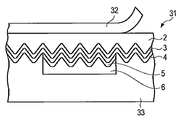
- FIG. 4 is a cross-sectional view showing an anti-counterfeit transfer foil.
- the anti-counterfeit transfer foil 31 includes a peelable support base 32, a relief forming layer 2, a first reflective layer 3, a functional thin film layer 4, a second reflective layer 5, a protective layer 6, and an adhesive layer 33 laminated in this order. Has the structure.
- the anti-counterfeit transfer foil 31 is formed by pressing a heating medium such as a heat roll or a hot plate against the support base material 32 and heating the transfer medium to a transfer temperature to press the adhesive layer onto another base material to be transferred and a support base.
- the support base material 32 is peeled off at the interface between the material 32 and the relief forming layer 2.
- a peeling protective layer may be provided between the support base and the relief forming layer as necessary.
- a peeling protective layer is a layer for peeling off from a support base material smoothly and stably. For this reason, the release protective layer is made of a material having a good releasability with respect to the support substrate.
- the film substrate is preferable as the supporting substrate used for the anti-counterfeit sticker and the anti-counterfeit transfer foil.
- the film base material it is desirable to use a material that is hardly deformed or deteriorated by heat, pressure, or electromagnetic waves applied at the time of forming a fine uneven pattern (relief structure).
- a plastic film such as PET (polyethylene terephthalate), PEN (polyethylene naphthalate), PP (polypropylene) can be used.
- PET polyethylene terephthalate
- PEN polyethylene naphthalate
- PP polypropylene
- paper, synthetic paper, plastic multilayer paper, resin-impregnated paper, or the like may be used as the supporting substrate.
- FIG. 5 is a cross-sectional view showing a forgery prevention structure according to the second embodiment.
- the forgery prevention structure 41 has a structure in which a relief forming layer 42, a first reflective layer 43, a functional thin film layer 44, a second reflective layer 45, and a protective layer 46 are laminated in this order.
- One side of the relief forming layer 42 has a relief structure having a first relief 47 and a second relief 48 having a fine concavo-convex pattern that has an effect of diffracting, scattering, absorbing, and separating polarized light in at least a part of the wavelength region of visible light.
- the surface of the first relief 47 has a smaller uneven surface area than the surface of the second relief 48.
- the first relief 47 has a gentle shape with the concave and convex portions, and the interval between the concave and convex portions is wide.
- the second relief 48 has a concave portion and a convex portion that are steeper than the first relief 47, and the interval between the concave and convex portions is narrower than that of the first relief 47.
- the first reflective layer 43 and the functional thin film layer 44 are provided on the entire surface along the fine uneven surface of the relief structure (first and second reliefs 47 and 48).
- the second reflective layer 45 and the protective layer 46 are provided so as to cover only the surface of the functional thin film layer 44 of the first relief 47.
- the first region 49 is a region in which the first reflective layer 43, the functional thin film layer 44, the second reflective layer 45, and the protective layer 46 are laminated in this order on the uneven surface of the first relief 47 of the relief forming layer 42.
- a colored reflective layer is obtained in which at least a partial region of visible light interferes with three layers including the first reflective layer 43, the functional thin film layer 44, and the second reflective layer 45.
- the three layers can also obtain a reflective layer whose color tone changes depending on the observation angle, and a relief structure having a colorful reflective layer can be designed.
- the colored reflective layer exists only in the first region 49, and only the patterned second reflective layer 45 is colored. In the first region 49, the patterned second reflective layer 45 itself is colored. As a result, since the second reflective layer 45 itself is a colored pattern, the colored ink is patterned and printed, and the reflective layer is formed so as to match the colored pattern. It is possible to avoid misalignment.
- the second region 50 is a region where only the first reflective layer 43 and the functional thin film layer 44 are laminated on the fine uneven surface of the second relief 48 of the relief forming layer 42, and the second reflective layer 45 and the protective layer 46 are not present. It is. For this reason, also in the 2nd field 50, it is possible to acquire the achromatic optical effect by a relief structure.
- the first region 49 and the second region 50 have different relief structures (first region 49: first relief 47, second region 50: second relief 48, uneven surface area: first relief 47 surface ⁇ second relief 48. It is possible to obtain different optical effects. For example, both structures are reliefs of diffraction gratings, and have different uneven surface areas, resulting in regions of different color change effects.
- the forgery prevention structure 41 is a boundary of a relief structure in which the boundary between the first region 49 and the second region 50 is different, the pattern of the second reflective layer 45, the colored pattern, and the relief structure of the first region 49 There is no misalignment with the pattern (first relief 47).
- the anti-counterfeit structure 41 according to the second embodiment includes a colored reflection relief structure in the first region 49 and an achromatic reflection relief in the second region 50, or different colors between the first and second regions 49 and 50.
- the change effect can provide a more precise and complicated optical effect, and thus can exhibit a higher anti-counterfeit effect.
- a relief forming layer is formed on the entire surface of the support substrate.
- the relief forming layer can be formed by coating, for example, wet coating, on the support substrate.
- the relief forming layer may be the support substrate itself.
- a relief original plate made of metal or resin having an uneven shape is prepared, and the uneven shape of this original plate is transferred onto the surface of the relief forming layer to form a relief structure having a first relief and an uneven relief having the unevenness.
- the uneven surface area of the first relief surface is smaller than that of the second relief surface. That is, the first relief has a wider interval between the irregularities than the interval between the irregularities of the second relief.
- the shape transfer method may be a known method such as the pressing method, the casting method, or the photopolymer method described in the first embodiment, or a hybrid method combining these methods.
- the first reflective layer, the functional thin film layer, and the second reflective layer thin film layer are formed in this order on the relief structure surface of the relief forming layer.
- the first reflective layer and the functional thin film layer can be formed by known wet coating or dry coating.
- the thin film layer for the second reflective layer is preferably formed by dry coating.
- a protective layer functioning as an etching mask is formed on the second reflective layer thin film layer.
- the second reflective layer is formed by selectively removing the second reflective thin film layer with an etching treatment agent using the protective layer as a mask. That is, the second reflective film is formed while leaving the second reflective layer thin film in the region below the protective layer (first region 49), and the second reflective layer thin film layer in the other region (second region 50). Remove.
- the forgery prevention structure according to the second embodiment is manufactured through the first to third steps described above, but is not limited thereto.
- the patterning of the protective layer and the second reflective film can also be formed by another method as follows. This will be described with reference to FIG. After the second reflective layer thin film layer 51 is formed on the entire surface of the functional thin film layer 44 by a vapor deposition method such as vacuum deposition or sputtering, the protective layer 46 is formed by a vapor deposition method such as vacuum deposition or sputtering. Form on the entire surface. At this time, as shown in FIG.
- the relief structure of the relief forming layer 42 includes the first relief 47 and the second relief 48 having a concave and convex interval narrower than the relief 47, so the second reflective layer thin film layer 51 and the protective layer 46 is formed with a sufficient thickness in the first region 49 where the first relief 47 is located, and is thinly formed only at the tip of the concavo-convex convex portion in the second region 50 where the second relief 48 is located. For this reason, when the subsequent entire surface etching process is performed, the protective layer 46 and the thin film layer 51 for the second reflective layer that are thinly formed only at the tips of the convex portions of the second region 50 are preferentially etched and removed. Only in one region 49, the second reflective layer thin film layer 51 (functioning as the second reflective layer 45) and the protective layer 46 remain and are patterned.
- the material of the protective layer 46 is a transparent inorganic material such as silica or alumina.
- the second reflective layer 45 (and the protective layer 46) can be formed on the first relief (first region) in a self-aligned manner in accordance with the shapes of the first and second reliefs 47 and 48 set in advance. For this reason, it is possible to color only the first region, and it is possible to obtain the optical effect of the relief in which the first region and the second region are different.
- each layer constituting the forgery prevention structure according to the second embodiment is the same as those described in the first embodiment.
- the anti-counterfeit structure according to the second embodiment may be another mode as shown in FIG. 3 (anti-counterfeit sticker) and FIG. 4 (anti-counterfeit transfer foil).
- an anti-counterfeit sticker and an anti-counterfeit transfer foil By using such an anti-counterfeit sticker and an anti-counterfeit transfer foil, an anti-counterfeit medium having an anti-counterfeit structure attached thereto can be obtained.
- the relief forming layer 2 was formed by applying and drying an ink composed of the following composition on a support 11 composed of a transparent polyethylene terephthalate (PET) film having a thickness of 25 ⁇ m and drying it so that the film thickness after drying was 2 ⁇ m. Subsequently, a relief pattern of a diffraction grating was formed on the surface of the relief forming layer 2 by a roll embossing method.
- PET polyethylene terephthalate
- Titanium oxide (TiO 2 ) is vacuum deposited on the relief forming layer 2 to form a first reflective layer 3 having a thickness of 50 nm along the relief pattern, and silica (SiO 2 ) is vacuum deposited on the first reflective layer 3.
- a functional thin film layer 4 having a thickness of 130 nm was formed.
- aluminum was vacuum deposited on the functional thin film layer 4 to form an aluminum layer having a thickness of 50 nm.
- the ink which consists of the following composition was printed on the aluminum layer with the gravure printing method, and the protective layer 6 of the star-shaped pattern was formed.
- the thickness of the protective layer 6 was 1 ⁇ m as a dry film thickness.
- the exposed aluminum layer portion was etched by performing an alkali etching process using the protective layer 6 as an etching mask to form a second reflective layer 5 having a star pattern.
- the ink which consists of the following composition was printed on the functional thin film layer 4 containing the protective layer 6 by the gravure printing method, and it dried and formed the contact bonding layer 23 with a film thickness of 3 micrometers, and the forgery prevention sticker 21 was obtained.
- a relief forming layer 103 was formed on the base material 101 including the colored layer 102 by the same method as in Example 1, and a relief structure 104 having fine irregularities on one side of the relief forming layer 103 was formed.
- aluminum was vacuum-deposited on the relief forming layer 103 to form an aluminum layer (not shown) having a thickness of 50 nm.
- the protective layer ink composition similar to Example 1 was printed on the aluminum layer by the gravure printing method, and the protective layer 105 of the star pattern was formed.
- the thickness of the protective layer 105 was 1 ⁇ m in terms of dry film thickness.
- the reflective layer 106 was formed by etching the exposed aluminum layer portion by performing alkali etching using the protective layer 105 as an etching mask (shown in FIG. 7B). Thereafter, although not shown, the same adhesive layer ink composition as in Example 1 is printed on the concavo-convex surface of the relief forming layer including the protective layer in the same manner as in Example 1 by the gravure printing method, and dried to form an adhesive layer having a thickness of 3 ⁇ m. Formed a forgery prevention sticker.
- the colored pattern of the star pattern and the protective layer of the star pattern were aligned as much as possible by reprinting with a gravure printing machine (overlapping register printing).
- the area ratio (mm 2 / mm 2 ) and the positional deviation width (mm) were measured at 20 locations, and the average value and the maximum value were obtained.
- the forgery prevention structure of Example 1 is good when the area ratio is 1.00 and the positional deviation is 0.00 mm (less than 0.01 mm below the measurement limit).
- the anti-counterfeit structure 1 has an area ratio of 1.02 and a positional deviation of 1.00 mm at the maximum.
- the anti-counterfeit structure with a desired color tone and an anti-counterfeit which is excellent in design property and / or security property regarding the anti-counterfeit structure having high design property and high security property. Since the structure can be provided, it can be used for securities, branded products, certificates, personal authentication media, and the like.
Landscapes
- Physics & Mathematics (AREA)
- General Physics & Mathematics (AREA)
- Engineering & Computer Science (AREA)
- Manufacturing & Machinery (AREA)
- Optics & Photonics (AREA)
- Computer Security & Cryptography (AREA)
- Business, Economics & Management (AREA)
- Accounting & Taxation (AREA)
- Finance (AREA)
- Credit Cards Or The Like (AREA)
- Diffracting Gratings Or Hologram Optical Elements (AREA)
- Chemical & Material Sciences (AREA)
- Chemical Kinetics & Catalysis (AREA)
- General Chemical & Material Sciences (AREA)
- Holo Graphy (AREA)
- Decoration By Transfer Pictures (AREA)
- Inspection Of Paper Currency And Valuable Securities (AREA)
- Health & Medical Sciences (AREA)
- General Health & Medical Sciences (AREA)
- Toxicology (AREA)
Abstract
L'invention concerne une structure de prévention de contrefaçon par laquelle au moins une couche de formation de relief, une première couche réfléchissante, une couche de film mince fonctionnel, une deuxième couche réfléchissante et une couche protectrice sont stratifiées dans cet ordre, et caractérisée en ce qu'un côté de la couche de formation de relief présente une structure en relief possédant des effets de diffraction, de diffusion, d'absorption et de séparation de polarisation sur au moins une partie de la région de longueur d'onde de la lumière visible. La première couche réfléchissante et la couche de film mince fonctionnel sont placées sur toute la surface le long des irrégularités de la structure en relief, la deuxième couche réfléchissante est placée sur une partie de recouvrement de région donnée des irrégularités de la structure en relief, la couche protectrice est disposée de telle sorte qu'elle couvre seulement la région de la deuxième couche réfléchissante, et les trois couches comprenant la première couche réfléchissante, la couche de film mince fonctionnel et la deuxième couche réfléchissante, sont autorisées à empiéter sur au moins une région de la lumière visible.
Priority Applications (7)
| Application Number | Priority Date | Filing Date | Title |
|---|---|---|---|
| PL12788957T PL2717102T3 (pl) | 2011-05-25 | 2012-05-24 | Barwna konstrukcja zapobiegająca fałszowaniu i barwny środek zapobiegający fałszowaniu |
| AU2012259820A AU2012259820B2 (en) | 2011-05-25 | 2012-05-24 | Colored counterfeit prevention structure and colored counterfeit prevention medium |
| CN201280025368.2A CN103562803B (zh) | 2011-05-25 | 2012-05-24 | 着色防伪结构体及着色防伪介质 |
| EP17192025.9A EP3285122B1 (fr) | 2011-05-25 | 2012-05-24 | Structure et support de prévention de falsification de coloration |
| EP12788957.4A EP2717102B1 (fr) | 2011-05-25 | 2012-05-24 | Structure colorée de prévention de contrefaçon et moyen coloré de prévention de contrefaçon |
| US14/087,838 US9354364B2 (en) | 2011-05-25 | 2013-11-22 | Coloring forgery prevention structure and coloring forgery prevention medium |
| US15/141,359 US10099503B2 (en) | 2011-05-25 | 2016-04-28 | Coloring forgery prevention structure and coloring forgery prevention medium |
Applications Claiming Priority (2)
| Application Number | Priority Date | Filing Date | Title |
|---|---|---|---|
| JP2011-116827 | 2011-05-25 | ||
| JP2011116827A JP5929013B2 (ja) | 2011-05-25 | 2011-05-25 | 着色偽造防止構造体および着色偽造防止媒体 |
Related Child Applications (1)
| Application Number | Title | Priority Date | Filing Date |
|---|---|---|---|
| US14/087,838 Continuation US9354364B2 (en) | 2011-05-25 | 2013-11-22 | Coloring forgery prevention structure and coloring forgery prevention medium |
Publications (1)
| Publication Number | Publication Date |
|---|---|
| WO2012161257A1 true WO2012161257A1 (fr) | 2012-11-29 |
Family
ID=47217329
Family Applications (1)
| Application Number | Title | Priority Date | Filing Date |
|---|---|---|---|
| PCT/JP2012/063338 Ceased WO2012161257A1 (fr) | 2011-05-25 | 2012-05-24 | Structure colorée de prévention de contrefaçon et moyen coloré de prévention de contrefaçon |
Country Status (7)
| Country | Link |
|---|---|
| US (2) | US9354364B2 (fr) |
| EP (2) | EP2717102B1 (fr) |
| JP (1) | JP5929013B2 (fr) |
| CN (2) | CN103562803B (fr) |
| AU (1) | AU2012259820B2 (fr) |
| PL (1) | PL2717102T3 (fr) |
| WO (1) | WO2012161257A1 (fr) |
Cited By (3)
| Publication number | Priority date | Publication date | Assignee | Title |
|---|---|---|---|---|
| US20160052327A1 (en) * | 2013-04-08 | 2016-02-25 | Toppan Printing Co., Ltd. | Anti-counterfeit medium, method for manufacturing the same and method for preventing counterfeiting |
| JPWO2020209331A1 (fr) * | 2019-04-09 | 2020-10-15 | ||
| WO2020224352A1 (fr) * | 2019-05-05 | 2020-11-12 | 中钞特种防伪科技有限公司 | Élément anti-contrefaçon optique de placage multicouche et son procédé de fabrication |
Families Citing this family (27)
| Publication number | Priority date | Publication date | Assignee | Title |
|---|---|---|---|---|
| JP5929013B2 (ja) | 2011-05-25 | 2016-06-01 | 凸版印刷株式会社 | 着色偽造防止構造体および着色偽造防止媒体 |
| CN105015216B (zh) * | 2014-04-29 | 2017-06-16 | 中钞特种防伪科技有限公司 | 一种光学防伪元件及制备光学防伪元件的方法 |
| CN105015215B (zh) * | 2014-04-30 | 2017-05-31 | 中钞特种防伪科技有限公司 | 光学防伪元件及其制造方法 |
| KR20170012353A (ko) * | 2014-05-26 | 2017-02-02 | 도판 인사츠 가부시키가이샤 | 위조 방지 구조체 및 위조 방지 물품 |
| EP3220171B1 (fr) * | 2014-11-10 | 2022-04-27 | Toppan Printing Co., Ltd. | Élément optique anti-contrefaçon |
| CN105984268B (zh) * | 2015-02-13 | 2021-11-05 | 龙璟印刷(深圳)有限公司 | 立体压凸水晶贴纸及其方法 |
| CN112859222B (zh) * | 2015-06-02 | 2022-08-12 | 凸版印刷株式会社 | 层叠体及其制造方法 |
| JP6707926B2 (ja) * | 2016-03-16 | 2020-06-10 | 凸版印刷株式会社 | 識別システム、識別方法及びプログラム |
| CN109313293B (zh) * | 2016-05-24 | 2021-12-28 | 恩希爱(杭州)薄膜有限公司 | 一种防伪反射片及其制备方法 |
| CN109152259A (zh) * | 2017-06-27 | 2019-01-04 | 昇印光电(昆山)股份有限公司 | 一种光学薄膜、模具及电子设备盖板 |
| CN109895526B (zh) * | 2017-12-08 | 2021-06-22 | 中钞特种防伪科技有限公司 | 光学防伪元件及其制作方法 |
| EP3770653B1 (fr) | 2018-03-20 | 2025-07-09 | Toppan Printing Co., Ltd. | Élément optique et corps d'authentification |
| WO2019221019A1 (fr) * | 2018-05-17 | 2019-11-21 | 凸版印刷株式会社 | Dispositif de sécurité, feuille de transfert et article attaché à un dispositif de sécurité |
| US10705268B2 (en) * | 2018-06-29 | 2020-07-07 | Applied Materials, Inc. | Gap fill of imprinted structure with spin coated high refractive index material for optical components |
| US20200003937A1 (en) * | 2018-06-29 | 2020-01-02 | Applied Materials, Inc. | Using flowable cvd to gap fill micro/nano structures for optical components |
| JP7192277B2 (ja) * | 2018-07-10 | 2022-12-20 | 凸版印刷株式会社 | 転写シート、発色シート、発色物品、および、転写方法 |
| CN110712452B (zh) * | 2018-07-13 | 2021-03-12 | 中钞特种防伪科技有限公司 | 光学防伪元件及其制备方法和光学防伪产品 |
| JP7358730B2 (ja) * | 2018-10-03 | 2023-10-11 | 凸版印刷株式会社 | 発色構造体 |
| JP7227403B2 (ja) * | 2019-04-28 | 2023-02-21 | レイア、インコーポレイテッド | 回折バックライト製造方法 |
| CN112572018B (zh) * | 2019-09-29 | 2022-06-14 | 中钞特种防伪科技有限公司 | 多层体光学防伪元件及其制作方法 |
| EP3859795B1 (fr) | 2020-01-28 | 2026-03-18 | Cnbm Research Institute For Advanced Glass Materials Group Co., Ltd. | Composant coloré tabulaire pourvu de plaque de recouvrement structurée et couche de filtre chromatique |
| JP7080952B2 (ja) * | 2020-10-21 | 2022-06-06 | 凸版印刷株式会社 | 転写箔及びその製造方法 |
| CN114891367A (zh) * | 2021-01-26 | 2022-08-12 | 中钞特种防伪科技有限公司 | 片状光学颜料及其制备方法、以及防伪元件 |
| CN113415092B (zh) * | 2021-05-24 | 2022-09-27 | 捷德(中国)科技有限公司 | 卡片制作方法和卡片 |
| BG67660B1 (bg) * | 2021-09-21 | 2024-10-15 | Демакс-Холограми Ад | Цветно холографско фолио |
| CN120913489A (zh) * | 2023-06-06 | 2025-11-07 | 中国印钞造币集团有限公司 | 光变防伪元件 |
| WO2025078330A1 (fr) * | 2023-10-13 | 2025-04-17 | Leonhard Kurz Stiftung & Co. Kg | Élément multicouche et procédé de production d'un élément multicouche |
Citations (9)
| Publication number | Priority date | Publication date | Assignee | Title |
|---|---|---|---|---|
| JP2524092Y2 (ja) | 1991-02-26 | 1997-01-29 | 凸版印刷株式会社 | ホログラムシート |
| US20030058491A1 (en) * | 2000-06-28 | 2003-03-27 | Holmes Brian William | Optically variable security device |
| JP4088884B2 (ja) | 2002-03-20 | 2008-05-21 | 日本ビクター株式会社 | 光ディスクの製造方法 |
| JP2008162260A (ja) | 2006-12-04 | 2008-07-17 | Dainippon Printing Co Ltd | ホログラム構造 |
| JP4194073B2 (ja) | 2002-09-25 | 2008-12-10 | 大日本印刷株式会社 | 光回折構造体 |
| JP2009086192A (ja) * | 2007-09-28 | 2009-04-23 | Toppan Printing Co Ltd | 偽造防止構造体及びそれを用いた偽造防止枚葉体、並びにその真偽判定方法 |
| JP2010099929A (ja) * | 2008-10-23 | 2010-05-06 | Toppan Printing Co Ltd | セキュリティフィルム、転写箔及び印刷物 |
| JP2010175812A (ja) | 2009-01-29 | 2010-08-12 | Toppan Printing Co Ltd | 偽造防止媒体 |
| WO2010147185A1 (fr) * | 2009-06-18 | 2010-12-23 | 凸版印刷株式会社 | Élément optique et procédé pour sa fabrication |
Family Cites Families (16)
| Publication number | Priority date | Publication date | Assignee | Title |
|---|---|---|---|---|
| US5128779A (en) * | 1988-02-12 | 1992-07-07 | American Banknote Holographics, Inc. | Non-continuous holograms, methods of making them and articles incorporating them |
| JPH04194073A (ja) | 1990-11-24 | 1992-07-14 | Kanebo Ltd | 加工布の移行に対する堅牢度試験方法および装置 |
| JP2524092B2 (ja) | 1994-05-12 | 1996-08-14 | 株式会社クボタ | 田植機の苗縦送り装置 |
| JPH1084137A (ja) | 1996-09-06 | 1998-03-31 | Omron Corp | 発光デバイスおよびその製造方法 |
| US7667895B2 (en) * | 1999-07-08 | 2010-02-23 | Jds Uniphase Corporation | Patterned structures with optically variable effects |
| US6987590B2 (en) * | 2003-09-18 | 2006-01-17 | Jds Uniphase Corporation | Patterned reflective optical structures |
| US6761959B1 (en) * | 1999-07-08 | 2004-07-13 | Flex Products, Inc. | Diffractive surfaces with color shifting backgrounds |
| EP1503906B1 (fr) * | 2002-05-14 | 2011-11-23 | Leonhard Kurz Stiftung & Co. KG | Element optiquement variable comportant un element partiel transparent |
| DE102004016596B4 (de) * | 2004-04-03 | 2006-07-27 | Ovd Kinegram Ag | Sicherheitselement in Form eines mehrschichtigen Folienkörpers und Verfahren zur Herstellung eines Sicherheitselements |
| JP4390265B2 (ja) * | 2004-04-14 | 2009-12-24 | 大日本印刷株式会社 | 真偽判定用媒体、真偽判定用媒体ラベル、真偽判定用媒体転写シート、真偽判定可能なシート、および真偽判定可能な情報記録体 |
| JP2008083599A (ja) | 2006-09-28 | 2008-04-10 | Toppan Printing Co Ltd | 光学素子およびそれを用いた表示体 |
| DE102007034716A1 (de) * | 2007-07-23 | 2009-01-29 | Giesecke & Devrient Gmbh | Sicherheitselement |
| JP5239241B2 (ja) | 2007-07-25 | 2013-07-17 | 凸版印刷株式会社 | 光学材料保護用積層体、これを用いたエレクトロルミネッセンス光学素子、及び電気泳動式表示パネル |
| JP5169083B2 (ja) * | 2007-09-05 | 2013-03-27 | 凸版印刷株式会社 | 偽造防止積層体、偽造防止転写箔、偽造防止シール、偽造防止媒体、およびこれらの製造方法 |
| DE102008031325A1 (de) * | 2008-07-02 | 2010-01-07 | Giesecke & Devrient Gmbh | Sicherheitselement sowie Verfahren zu seiner Herstellung |
| JP5929013B2 (ja) | 2011-05-25 | 2016-06-01 | 凸版印刷株式会社 | 着色偽造防止構造体および着色偽造防止媒体 |
-
2011
- 2011-05-25 JP JP2011116827A patent/JP5929013B2/ja active Active
-
2012
- 2012-05-24 EP EP12788957.4A patent/EP2717102B1/fr not_active Not-in-force
- 2012-05-24 EP EP17192025.9A patent/EP3285122B1/fr active Active
- 2012-05-24 WO PCT/JP2012/063338 patent/WO2012161257A1/fr not_active Ceased
- 2012-05-24 CN CN201280025368.2A patent/CN103562803B/zh active Active
- 2012-05-24 PL PL12788957T patent/PL2717102T3/pl unknown
- 2012-05-24 AU AU2012259820A patent/AU2012259820B2/en active Active
- 2012-05-24 CN CN201610626666.7A patent/CN106199799B/zh active Active
-
2013
- 2013-11-22 US US14/087,838 patent/US9354364B2/en active Active
-
2016
- 2016-04-28 US US15/141,359 patent/US10099503B2/en active Active
Patent Citations (9)
| Publication number | Priority date | Publication date | Assignee | Title |
|---|---|---|---|---|
| JP2524092Y2 (ja) | 1991-02-26 | 1997-01-29 | 凸版印刷株式会社 | ホログラムシート |
| US20030058491A1 (en) * | 2000-06-28 | 2003-03-27 | Holmes Brian William | Optically variable security device |
| JP4088884B2 (ja) | 2002-03-20 | 2008-05-21 | 日本ビクター株式会社 | 光ディスクの製造方法 |
| JP4194073B2 (ja) | 2002-09-25 | 2008-12-10 | 大日本印刷株式会社 | 光回折構造体 |
| JP2008162260A (ja) | 2006-12-04 | 2008-07-17 | Dainippon Printing Co Ltd | ホログラム構造 |
| JP2009086192A (ja) * | 2007-09-28 | 2009-04-23 | Toppan Printing Co Ltd | 偽造防止構造体及びそれを用いた偽造防止枚葉体、並びにその真偽判定方法 |
| JP2010099929A (ja) * | 2008-10-23 | 2010-05-06 | Toppan Printing Co Ltd | セキュリティフィルム、転写箔及び印刷物 |
| JP2010175812A (ja) | 2009-01-29 | 2010-08-12 | Toppan Printing Co Ltd | 偽造防止媒体 |
| WO2010147185A1 (fr) * | 2009-06-18 | 2010-12-23 | 凸版印刷株式会社 | Élément optique et procédé pour sa fabrication |
Cited By (9)
| Publication number | Priority date | Publication date | Assignee | Title |
|---|---|---|---|---|
| US20160052327A1 (en) * | 2013-04-08 | 2016-02-25 | Toppan Printing Co., Ltd. | Anti-counterfeit medium, method for manufacturing the same and method for preventing counterfeiting |
| US9956805B2 (en) * | 2013-04-08 | 2018-05-01 | Toppan Printing Co., Ltd. | Anti-counterfeit medium, method for manufacturing the same and method for preventing counterfeiting |
| US10300731B2 (en) | 2013-04-08 | 2019-05-28 | Toppan Printing Co., Ltd. | Anti-counterfeit medium, method for manufacturing the same and method for preventing counterfeiting |
| JPWO2020209331A1 (fr) * | 2019-04-09 | 2020-10-15 | ||
| JP7619260B2 (ja) | 2019-04-09 | 2025-01-22 | Toppanホールディングス株式会社 | 光学構造体、転写箔、および物品 |
| WO2020224352A1 (fr) * | 2019-05-05 | 2020-11-12 | 中钞特种防伪科技有限公司 | Élément anti-contrefaçon optique de placage multicouche et son procédé de fabrication |
| JP2022532560A (ja) * | 2019-05-05 | 2022-07-15 | 中▲鈔▼特▲種▼防▲偽▼科技有限公司 | 多層メッキ層を備えた光学偽造防止素子及びその製造方法 |
| JP7376615B2 (ja) | 2019-05-05 | 2023-11-08 | 中▲鈔▼特▲種▼防▲偽▼科技有限公司 | 多層メッキ層を備えた光学偽造防止素子及びその製造方法 |
| US12233658B2 (en) | 2019-05-05 | 2025-02-25 | Zhongchao Special Security Technology Co., Ltd. | Multi-plating-layer optical anti-counterfeiting element and manufacturing method thereof |
Also Published As
| Publication number | Publication date |
|---|---|
| CN106199799A (zh) | 2016-12-07 |
| EP2717102B1 (fr) | 2017-11-29 |
| CN103562803A (zh) | 2014-02-05 |
| JP2012247483A (ja) | 2012-12-13 |
| AU2012259820B2 (en) | 2015-05-21 |
| CN106199799B (zh) | 2018-05-25 |
| US20140077487A1 (en) | 2014-03-20 |
| EP2717102A1 (fr) | 2014-04-09 |
| EP2717102A4 (fr) | 2015-06-10 |
| EP3285122B1 (fr) | 2019-07-10 |
| US20160237622A1 (en) | 2016-08-18 |
| PL2717102T3 (pl) | 2018-05-30 |
| US10099503B2 (en) | 2018-10-16 |
| EP3285122A1 (fr) | 2018-02-21 |
| JP5929013B2 (ja) | 2016-06-01 |
| CN103562803B (zh) | 2016-08-31 |
| US9354364B2 (en) | 2016-05-31 |
Similar Documents
| Publication | Publication Date | Title |
|---|---|---|
| JP5929013B2 (ja) | 着色偽造防止構造体および着色偽造防止媒体 | |
| JP5594043B2 (ja) | 偽造防止構造体、及び偽造防止媒体 | |
| JP6476863B2 (ja) | 偽造防止構造体及びその製造方法 | |
| JP5477046B2 (ja) | 表示体及びその製造方法 | |
| JP6269482B2 (ja) | 異方性反射表示体、並びに異方性反射表示体を用いた情報記録体 | |
| JP5169083B2 (ja) | 偽造防止積層体、偽造防止転写箔、偽造防止シール、偽造防止媒体、およびこれらの製造方法 | |
| KR20170012353A (ko) | 위조 방지 구조체 및 위조 방지 물품 | |
| CN111746171B (zh) | 光学防伪元件及其制作方法 | |
| JP5169093B2 (ja) | 偽造防止積層体、偽造防止転写箔、偽造防止シール、偽造防止媒体、及びこれらの製造方法 | |
| JP5717324B2 (ja) | 偽造防止構造体及びその製造方法 | |
| JP6187611B2 (ja) | 着色偽造防止構造体および着色偽造防止媒体 | |
| JP2011150003A (ja) | 光学素子及びその製造方法 | |
| JP4967566B2 (ja) | 転写シート | |
| JP2025124485A (ja) | 転写媒体および転写物の製造方法 |
Legal Events
| Date | Code | Title | Description |
|---|---|---|---|
| 121 | Ep: the epo has been informed by wipo that ep was designated in this application |
Ref document number: 12788957 Country of ref document: EP Kind code of ref document: A1 |
|
| NENP | Non-entry into the national phase |
Ref country code: DE |
|
| REEP | Request for entry into the european phase |
Ref document number: 2012788957 Country of ref document: EP |
|
| ENP | Entry into the national phase |
Ref document number: 2012259820 Country of ref document: AU Date of ref document: 20120524 Kind code of ref document: A |