WO2012164641A1 - Dispositif d'inspection de défauts optiques à champ proche - Google Patents
Dispositif d'inspection de défauts optiques à champ proche Download PDFInfo
- Publication number
- WO2012164641A1 WO2012164641A1 PCT/JP2011/062203 JP2011062203W WO2012164641A1 WO 2012164641 A1 WO2012164641 A1 WO 2012164641A1 JP 2011062203 W JP2011062203 W JP 2011062203W WO 2012164641 A1 WO2012164641 A1 WO 2012164641A1
- Authority
- WO
- WIPO (PCT)
- Prior art keywords
- slider
- light
- inspection
- wafer
- opening
- Prior art date
- Legal status (The legal status is an assumption and is not a legal conclusion. Google has not performed a legal analysis and makes no representation as to the accuracy of the status listed.)
- Ceased
Links
Images










Classifications
-
- G—PHYSICS
- G01—MEASURING; TESTING
- G01N—INVESTIGATING OR ANALYSING MATERIALS BY DETERMINING THEIR CHEMICAL OR PHYSICAL PROPERTIES
- G01N21/00—Investigating or analysing materials by the use of optical means, i.e. using sub-millimetre waves, infrared, visible or ultraviolet light
- G01N21/84—Systems specially adapted for particular applications
- G01N21/88—Investigating the presence of flaws or contamination
- G01N21/95—Investigating the presence of flaws or contamination characterised by the material or shape of the object to be examined
- G01N21/9501—Semiconductor wafers
- G01N21/9505—Wafer internal defects, e.g. microcracks
-
- G—PHYSICS
- G01—MEASURING; TESTING
- G01B—MEASURING LENGTH, THICKNESS OR SIMILAR LINEAR DIMENSIONS; MEASURING ANGLES; MEASURING AREAS; MEASURING IRREGULARITIES OF SURFACES OR CONTOURS
- G01B11/00—Measuring arrangements characterised by the use of optical techniques
- G01B11/30—Measuring arrangements characterised by the use of optical techniques for measuring roughness or irregularity of surfaces
-
- H—ELECTRICITY
- H10—SEMICONDUCTOR DEVICES; ELECTRIC SOLID-STATE DEVICES NOT OTHERWISE PROVIDED FOR
- H10P—GENERIC PROCESSES OR APPARATUS FOR THE MANUFACTURE OR TREATMENT OF DEVICES COVERED BY CLASS H10
- H10P74/00—Testing or measuring during manufacture or treatment of wafers, substrates or devices
- H10P74/20—Testing or measuring during manufacture or treatment of wafers, substrates or devices characterised by the properties tested or measured, e.g. structural or electrical properties
- H10P74/203—Structural properties, e.g. testing or measuring thicknesses, line widths, warpage, bond strengths or physical defects
Definitions
- the present invention relates to an apparatus for detecting a defect of an object to be inspected by near-field light, and particularly to a near-field optical defect inspection apparatus for detecting the defect by near-field light due to a defect inside the object to be inspected.
- wafers In silicon wafers (hereinafter referred to as “wafers”) used in semiconductors and solar cells, micro-defects (holes and foreign materials) of several nanometers to micron sizes that exist inside the wafers have become smaller in semiconductors and solar cells as the wiring and surface shape become finer. The effect on quality and performance is increasing.
- Patent Document 1 discloses a method for inspecting a defect existing inside a wafer instead of the surface of the wafer. In this method, infrared light is incident on a wafer, and scattered light generated in an internal defect portion is observed with a camera.
- Patent Document 1 makes it possible to detect defects existing inside a wafer by utilizing the infrared light transmission characteristics of silicon.
- this method using infrared light it is difficult to make the resolution in the in-plane direction of the wafer sufficiently smaller than the wavelength of the infrared light to be irradiated. Therefore, this method is not suitable for detecting a micro defect of several nano sizes on the wafer.
- a wafer is placed on a stage, and the stage is moved to scan the wafer with infrared light.
- mechanical vibration of the apparatus occurs when the stage is driven, and the distance between the measurement location of the wafer and the camera changes on the order of several microns.
- the above method is not suitable for detecting a micro defect of several nano sizes.
- the vibration increases when the stage is moved at high speed, it is difficult for the above method to complete the defect inspection of the entire wafer in a short time.
- the present invention has been made in view of the above circumstances, and has as its main object to accurately inspect the presence or absence of microdefects in an object to be inspected, such as a silicon wafer, and to shorten the inspection time. .
- the near-field light defect inspection apparatus of one embodiment of the present invention includes a motor, a slider, a slider moving mechanism, a light source, and a condensing probe.
- the motor rotates the object to be inspected.
- the slider slides on the rotating object to be inspected.
- the slider moving mechanism supports the slider and moves the slider on an object to be inspected that is rotated by a motor.
- the light source emits inspection light that is applied to the object to be inspected rotated by the motor and propagates through the object to be inspected.
- the condensing probe has an opening, and condenses near-field light due to a defect in the inspected body that has received the inspection light from the opening.
- the opening is formed on the surface of the slider facing the object to be inspected, and the maximum diameter is smaller than the wavelength of visible light.
- This embodiment will explain the defect inspection of an inspection object.
- an example of a micro defect inspection inside a silicon wafer will be described with inspection infrared light.
- the defect inspection of the present embodiment is particularly suitable for a silicon wafer (hereinafter referred to as a wafer), but can be applied to defect inspection of other inspection objects.
- An appropriate wavelength of the inspection light is selected depending on the material of the wafer.
- the defect inspection apparatus of this embodiment irradiates the wafer with infrared light having a wavelength that transmits silicon as inspection light. Infrared light propagates through the wafer repeatedly with total reflection. When infrared light propagating through the wafer hits a defect (such as a foreign object or a hole) inside the wafer, near-field light is generated around the defect. Some of the near-field light exists outside the wafer in the vicinity of the wafer surface.
- the defect inspection apparatus of this embodiment supports a slider having a probe that collects near-field light on a rotating wafer.
- the defect inspection apparatus collects near-field light generated by minute internal defects in the vicinity of the wafer surface by a slider (probe) that slides on the wafer, and detects defects inside the wafer.
- the defect inspection apparatus of this embodiment rotates a wafer and moves a slider in the radial direction on the rotating wafer. Thereby, the defect inspection of the whole wafer can be performed in a short time.
- the slider preferably floats on the wafer with a nano gap (several nanometers to several tens of nanometers).
- the slider may slide on the wafer in contact with the wafer. Thereby, a minute distance between the probe formed on the slider and the internal defect can be realized, and near-field light due to the minute defect inside the wafer can be detected appropriately.
- a plurality of embodiments of the nano-gap near-field optical defect inspection apparatus of the present invention will be described with reference to the drawings.
- FIG. 1A schematically shows a configuration example of a near-field light defect inspection apparatus 1 according to a first embodiment.
- the magnitude relation of the size of each displayed component is changed from the actual magnitude relation.
- X, Y, and Z coordinate axes are defined.
- the X axis is a directional axis from the left to the right of the paper
- the Y axis is a directional axis from the front of the paper to the back
- the Z axis is a directional axis from the bottom to the top of the paper.
- the relationship between these X, Y, and Z axes and the near-field optical defect inspection apparatus 1 is maintained in other drawings.
- the near-field light defect inspection apparatus 1 includes a spindle motor 2 that rotates a wafer 4 that is an object to be inspected and a slider 67 that slides on the rotating wafer 4.
- the slider 67 floats on the wafer 4 with a gap of several nanometers to several tens of nanometers.
- the wafer 4 is attached to the upper part of the spindle of the spindle motor 2, and the wafer 4 also rotates when the spinning rotates.
- a rotating disk is attached to the spindle, and the wafer 4 is placed on the disk.
- the wafer 4 is fixed to the disk by, for example, a locking part or a vacuum chuck.
- the mechanism for rotating the wafer 4 may have any configuration suitable for the rotation of the wafer 4.
- the slider 67 has a substantially rectangular parallelepiped slider body 6 and a multilayer element portion 7 formed on the slider body 6. Details of the configuration of the slider 67 will be described later.
- the slider 67 is supported by the suspension 5.
- the suspension 5 supports the slider 67 elastically.
- the suspension 5 includes, for example, a load beam made of stainless steel and a gimbal fixed to the load beam. The gimbal is fixed to a load beam by caulking or laser spot welding.
- the gimbal is fixed to the surface of the load beam facing the wafer 4, and the slider 67 is fixed to the surface of the load beam facing the wafer 4.
- the slider 67 is bonded to the gimbal by adhesive bonding, for example.
- the load beam functions as a precise thin plate spring and generates a load that opposes the flying force of the slider 67.
- the air that flows between the slider 67 and the wafer 4 due to the rotation of the wafer 4 generates a pressure for floating the slider 67.
- the surface of the slider body 6 facing the wafer 4 is processed into a desired shape.
- This surface functions as an air bearing surface and has a precisely designed uneven shape. Due to the effect of the air bearing surface, the slider 67 can move on the wafer 4 while maintaining a substantially constant distance from the wafer 4. Depending on the design, when the slider 67 is moved to an arbitrary position on the wafer 4, the slider 67 may slide in a state of being in slight contact with the wafer 4 so that the wafer 4 is not worn.
- a slider design used in a hard disk drive can be referred to.
- the gimbal is a flexible thin metal plate part that is easily deformed as compared with the load beam, and supports the slider 67 while realizing a free flight posture change on the slider 67 floating on the wafer 4.
- the suspension 5 may have any structure as long as the suspension slider 67 can be appropriately supported.
- a suspension used in a hard disk drive can be referred to.
- the suspension 5 is fixed to the movable support mechanism 3.
- the movement support mechanism 3 includes a three-axis stage that can move in the X-axis, Y-axis, and Z-axis directions, and supports the suspension 5 at the tip of an arm formed on the top.
- the suspension 5 is fixed to the arm of the movement support mechanism 3.
- the near-field light defect inspection apparatus 1 has a control management system including a signal processing circuit 51, a controller 52, and a management computer 53.
- the signal processing circuit 51 processes the electrical signal from the slider 67 and transmits the result to the management computer 53. Specifically, an electrical signal converted from near-field light due to a defect in the wafer 4 detected by the slider 67 is transmitted to the signal processing circuit 51.
- the signal processing circuit analyzes the signal and notifies the management computer 53 of the presence or absence of a defect.
- the controller 52 drives and controls the spindle motor 2 and the movement support mechanism 3 in accordance with instructions from the management computer 53.
- the controller 52 moves the suspension 5 and the slider 67 on the wafer 4 by the three-axis stage of the movement support mechanism 3 while the spindle motor 2 to which the wafer 4 is fixed is rotated or stationary.
- the controller 52 can move the slider 67 to an arbitrary position on the wafer 4 by controlling the movement of the movement support mechanism 3.
- the controller 52 can specify the current position of the slider 67 on the wafer 4 from the current position of the moving support mechanism 3.
- the management computer 53 acquires information indicating the current position of the slider 67 from the controller 52.
- the management computer 53 can specify the presence / absence of a defect on the wafer 4 and the position of the defect from the defect information of the signal processing circuit 51 and the slider position information from the controller 52.
- the movement support mechanism 3 is a three-axis stage of X-axis, Y-axis, and Z-axis, a two-axis stage of X-axis and Y-axis, or a single-axis stage configured by one of the X-axis and Y-axis You may have.
- the movement support mechanism 3 may be a rotation stage having a rotation axis around the Z axis. In this configuration, the suspension 5 rotates in the radial direction of the wafer 4 about the Z-axis direction (rotation axis direction of the wafer 4), so that the slider 67 is in an arbitrary direction in the direction perpendicular to the rotation axis of the wafer 4. Can move to a position.
- FIG. 1B schematically shows the near-field light defect inspection apparatus 1 of this embodiment viewed from the positive direction of the Z axis.
- the wafer 4 rotates counterclockwise as viewed from the slider 67. That is, the wafer 4 is rotated in the direction from the base of the suspension 5 (fixed position with the moving support mechanism 3) toward the tip thereof. Therefore, the slider 67 slides relative to the wafer 4 in the direction from the tip of the suspension 5 toward the moving support mechanism 3.
- the laminated element portion 7 is formed on the trailing end face of the slider body 6.
- the trailing end surface is at a position lower than the other side surfaces (not including the wafer facing surface).
- the laminated element portion 7 is preferably formed on the trailing end surface, but may be formed on another surface.
- the rotation direction of the wafer 4 is an example, and may be rotated in the opposite direction.
- the controller 52 controls the spindle motor 2 to rotate or change the rotational speed of the wafer 4 at a constant rotational speed.
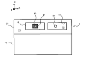
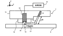
- FIG. 2A schematically shows the details of the multilayer element portion 7 and the positional relationship between the multilayer element portion 7 and the wafer 4, and is a view of the multilayer element portion 7 as seen from the positive side of the X axis.
- FIG. 2B schematically shows a part of the multilayer element portion 7 and the slider main body 6 as seen from the negative side of the Z-axis.
- the slider body 6 is made of a material such as silicon or Altic.
- the uneven shape of the air bearing surface of the slider body 6 is omitted.
- the laminated element portion 7 is formed by being laminated on the trailing end face of the slider body 6. That is, in FIG. 2B, the multilayer element portion 7 is formed by laminating a plurality of layers in the direction from the negative to the positive of the X axis.
- the method for forming the laminated element portion 7 is not a feature of the present embodiment, and thus the description thereof is omitted.
- the slider 67 of the present embodiment can be manufactured by a technique used in manufacturing a head slider of a hard disk drive, but the slider 67 may be manufactured by any method.
- the laminated element portion 7 has a light emitting portion 8 that emits inspection light for the wafer 4, in this example, infrared light.
- the light emitting unit 8 is, for example, a laser diode.
- the frequency of the infrared light depends on the material of the wafer 4, and the frequency of the infrared light for silicon inspection is included in, for example, 1000 nm to 10 ⁇ m.
- the laminated element unit 7 includes a light emitting unit 8 that is a light source, but the light emitting unit 8 may be configured by a light emitting element and an optical waveguide such as an optical fiber. Further, the light emitting element may be disposed on another surface of the slider body 6 or a part different from the slider 67, for example, the suspension 5. In this case, the laminated element unit 7 has an optical waveguide, and light from the light emitting element propagates in the waveguide.
- the laminated element unit 7 includes a condensing probe 90 that collects near-field light 19 due to the defect 18 inside the wafer 4.
- the condensing probe 90 includes the light receiving unit 10 and the light shielding film 91.
- the light receiving unit 10 includes, for example, an optical fiber and a photoelectric conversion element.
- the light receiving element is typically a photodiode.
- the light receiving unit 10 may be an infrared optical waveguide including an optical fiber that receives and transmits light without including an active element that converts light into an electrical signal.
- the conversion element is disposed on the other surface of the slider body 6 or another component, for example, the suspension 5.
- a light shielding film 91 is attached to the tip of the light receiving unit 10.
- the light shielding film 91 shields the infrared light for inspection, and usually shields visible light.
- the material of the light shielding film 91 is, for example, an alloy containing gold, silicon dioxide, iron, cobalt, or the like.
- an opening 92 is formed in the light shielding film 91. Near-field light 19 due to the defect 18 enters the light receiving unit 10 through the opening 92.
- the laminated element portion 7 is formed around the light emitting portion 8 and the condensing probe 90, and has an element body portion 71 that includes them.
- the element body 71 is an alloy containing alumina as a main material and containing an impurity metal element, for example.
- the material of the element body 71 is a material that does not transmit infrared light for inspection and shields it. In general, the material of the element body 71 blocks visible light.
- a protrusion 12 is formed around the tip of the light receiving unit 10.
- the front end surface of the light receiving unit 10 is covered with a light shielding film 91 except for the opening 92, but the side surface of the front end unit is covered with the protruding portion 12.
- the protrusion 12 is formed of the same or different material as the element body 71. Similar to the light shielding film 91, the protruding portion 12 shields the infrared light for inspection and generally shields visible light.
- the controller 52 controls the light emitting unit 8, and the infrared light 16 emitted from the light emitting unit 8 enters the wafer 4 and becomes total reflection light 17 that undergoes total reflection inside the wafer 4. If a minute defect 18 due to a hole or a foreign substance exists inside the wafer 4, the angle of the total reflected light 17 changes, and a near-field light 19 due to the minute defect 18 is generated on the surface of the wafer 4.
- the near-field light 19 enters the minute opening 92 of the condensing probe 90 and is detected by the light receiving unit 10.
- the near-field light 19 detected by the light receiving unit 10 is converted into an electric signal by the light receiving unit 10 and is taken into the signal processing circuit 51 through the wiring.
- the signal processing circuit 51 performs processing for obtaining the intensity of the near-field light 19.
- Near-field light is light that is generated only on the surface of a minute particle (small defect 18 in this example), and therefore cannot be detected by a normal photodiode.
- the near-field light caused by the minute defect 18 can be detected by bringing the minute opening 92 close to the surface of the wafer 4.
- the element body 71 has a hole 11 formed therein.
- the light irradiation port 81 of the light emitting unit 8 is exposed on the bottom surface 72 of the hole 11.
- the inspection infrared light 16 is irradiated from the light irradiation port 81 toward the wafer 4.
- the hole 11 is surrounded by a wall.
- the space of the hole 11 is a rectangular parallelepiped.
- the hole 11 may have a different shape, and is formed in an appropriate shape by design.
- at least one of the wall surface and the bottom surface 72 may be a curved surface instead of a flat surface.
- the distance 13B in the light irradiation direction from the light irradiation port 81 of the light emitting unit 8 to the surface of the wafer 4 is longer than the wavelength of the infrared light for inspection.
- the infrared light for inspection can be appropriately propagated inside the wafer 4.
- An appropriate value is selected as the irradiation angle of the inspection infrared light, that is, the incident angle to the surface of the wafer 4 so that the inspection infrared light is totally reflected inside the wafer 4.
- the infrared light approaches the probe 90 as it travels from the light irradiation port toward the wafer surface 4 so that the near-field light due to the defect can be detected (the irradiation direction vector has a component toward the opening 92). Including).
- the light emitting unit 8 and the light receiving unit 10 are arranged side by side in the Y-axis direction, the light receiving unit 10 is on the outer peripheral side of the wafer 4 surface, and the light emitting unit 8 is on the inner peripheral side.
- the positional relationship between the light receiving unit 10 and the light emitting unit 8 may be different from this.
- the light emitting unit 8 may be on the outer peripheral side and the light receiving unit 10 may be on the inner peripheral side. These may be arranged side by side in the X direction.
- the light emitting unit 8 may be on the leading side and the light receiving unit 10 may be on the trailing side. These may be arranged obliquely in the YX plane.
- the light irradiation port 81 of the light emitting unit 8 is formed in the hole 11.
- the distance between the light irradiation port 81 and the wafer 4 can be increased while the distance between the reference surface 73 of the element main body 71 and the surface of the wafer 4 is reduced.
- the maximum distance 13A between the multilayer element portion 7 and the wafer 4 surface outside the hole 11, that is, in the example of FIG. 2A, the maximum rejection distance 13A between the reference surface 73 and the wafer 4 surface is the wavelength of visible light. Smaller than. Specifically, it is smaller than 360 nm. Thereby, the stray light which becomes noise and reaches the light receiving unit 10 can be reduced.
- the distance between the wafer surface 4 and the laminated element portion 7 (of the wafer facing surface) differs depending on the position in addition to the shape. Typically, while the slider 67 is sliding on the wafer 4, the slider 67 is tilted and the trailing end is lower than the leading end. Further, the wafer facing surface of the multilayer element portion 7 may have a shape different from the shape shown in FIGS. 2A and 2B, for example, a surface having more different depths (heights). Also good.
- the maximum distance between the multilayer element portion 7 outside the hole 11 and the surface of the wafer 4 is the distance between the multilayer element portion 7 outside the hole 11 and the surface of the wafer 4 during the defect inspection while irradiating infrared rays. It is the maximum value of the distance.
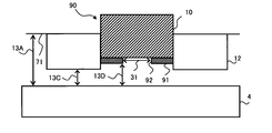
- FIG. 3A schematically shows the opening 92 at the tip of the condensing probe 90 (on the wafer facing surface) and the configuration around it.
- the resolution of the near-field light defect device is determined not by the wavelength of the infrared light for inspection but by the size of the opening 92.
- the aperture 92 is designed to have an appropriate size in order to collect near-field light of a minute defect intended for detection.
- the diameter (maximum diameter) 31 of the opening 92 is smaller than the wavelength of visible light. Specifically, it is smaller than 360 nm, preferably smaller than 100 nm. Thereby, the near field light of a micro defect can be detected appropriately.
- the shape of the opening 92 shown in FIG. 2B is a circle. As shown in FIG. 3B, the diameter of the circular opening 92 is the diameter.
- the opening 92 may have other shapes.
- the shape may be an ellipse as shown in FIG. 3C
- the shape may be a square as shown in FIG. 3D
- the shape is a triangle as shown in FIG. 3E. Also good.
- the diameter 31 is a major axis.
- the shape of the opening 92 is a quadrangle
- the diameter 31 is a longer straight line among the straight lines connecting the opposing angles.
- the shape of the opening 92 is a triangle
- the diameter 31 is a longer straight line among the straight lines on each side.
- the distance 13D between the opening 92 and the wafer 4 is sufficiently small in order for the opening 92 to appropriately collect near-field light due to the defect. Therefore, in a preferred configuration, the distance 13 ⁇ / b> D between the opening 92 and the wafer 4 is shorter than the maximum diameter 31 of the opening 92.
- the optical fiber at the tip of the condensing probe 90 protrudes from the element main body 71 toward the wafer 4.
- the light shielding film 91 covers the wafer facing surface at the tip of the condensing probe 90 with a region other than the opening 92, but does not adhere to the side surface.
- the side surface is covered with a protruding portion 12 that protrudes from the element main body portion 71 toward the wafer 4.
- the protrusion 12 shields the inspection infrared light and visible light.
- the tip of the protruding portion 12 protrudes from the opening 92 of the condensing probe 90 and is in a position close to the wafer 4.
- the opening 92 of the condensing probe 90 can be brought close to the wafer 4 and collision between the condensing probe 90 and the wafer 4 can be prevented.
- the protrusion 12 can reduce stray light from the surroundings to the opening 92.
- the distance (maximum distance) 13C between the protrusion 12 and the wafer 4 is preferably shorter than the wavelength of visible light, and is preferably shorter than the diameter 31 of the opening 92. When the distance 13C varies depending on the position of the protrusion 12 on the wafer facing surface, the maximum value is the distance 13C.
- the protruding portion 12 surrounds the periphery of the tip of the condensing probe 90 (periphery in the XY plane that is a surface facing the wafer 4), and the wafer facing surface is a quadrangle.
- the protrusion 12 is not limited to this.
- the protrusion 12 may have any shape such as a polygon or a circle when viewed in the Z-axis direction, and the wafer facing surface may be a curved surface.
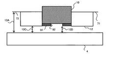
- the protruding portion 12 protrudes to a position closer to the wafer 4 than the tip of the condensing probe 90.
- the tip of the protruding portion 12 and the tip of the condensing probe 90 may be flat, or the distance 13C between the protruding portion 12 and the wafer 4 is the condensing probe 90.
- the distance between the opening 92 and the wafer 4 may be 13D or more.
- the entire tip of the condensing probe 90 protruding from the element main body 71 may be covered with a light shielding film 91 having an opening 92 without forming the protruding portion 12.
- the protrusion 12 is preferably formed so as to surround the entire periphery of the tip of the condensing probe 90 in the XY plane, but may be formed so as to surround a part thereof.
- a portion of the tip of the condensing probe 90 that is not covered with the protruding portion 12 is covered with a light shielding film 91.
- the near-field light defect inspection apparatus 1 may use non-vibrated infrared light 16, but may use infrared light that vibrates at a specific frequency in order to improve defect detection accuracy.
- the controller 52 vibrates the output of the infrared light 16 from the light emitting unit 8 at a specific frequency.
- the signal processing circuit 51 uses a lock-in amplifier to extract only the excited frequency component. Thereby, the influence of disturbance light can be suppressed.
- the light receiving unit 10 described above includes a combination of an optical fiber and a photodiode, but other elements may be used as long as the light receiving element can detect light.
- high-speed processing can be performed by using the signal processing circuit 51 in addition to the management computer 53.
- the management computer 53 may execute processing equivalent to the processing performed by the signal processing circuit 51. .
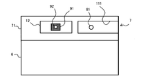
- the light irradiation port 81 of the light emitting unit 8 is preferably surrounded by a wall and exposed at the bottom of the hole 11. Unlike this, for example, as shown in FIGS. 5A and 5B, the irradiation port 81 of the light emitting unit 8 may be located in the recess 111 that continues to the end of the multilayer element unit 7. This shape is inferior in the effect of becoming a noise source and preventing light from the surroundings as compared with the above example, but the laminated element portion 7 is easy to process.
- FIGS. 6A and 6B show another configuration example of the laminated element unit 7.
- the protrusion 12 reaches the trailing end (end in the positive X-axis direction) and both ends in the Y-axis direction of the wafer facing surface of the multilayer element unit 7.
- the protrusion 12 surrounds the entire periphery of the condensing probe 90 and the entire periphery of the hole 11.
- the configuration shown in FIGS. 2A and 2B is preferable, but this shape facilitates processing of the laminated element portion 7.
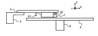
- FIG. 7 shows another configuration example of the multilayer element unit 7 of the near-field light defect inspection apparatus 1.
- the laminated element unit 7 includes a heater element 20.
- the heater element 20 is, for example, a thin film resistance element formed of permalloy. Other configurations are the same as those described in the first embodiment.
- the heater element 20 is driven and controlled by the controller 52 via the connection pad at the trailing end of the multilayer element portion 7.
- the controller 52 applies power to the heater element 20 from the connection pad, the heater element 20 generates heat.
- the temperature of the laminated element portion 7 rises around the heater element 20, and the laminated element portion 7 expands.
- the portion provided with the minute opening 92 expands toward the wafer 4, and the gap 13 ⁇ / b> D between the wafer 4 and the minute opening 92 is reduced.
- the controller 52 can control and fine-tune the gap 13D by changing the power applied to the heater element 20.
- a suitable position of the heater element 20 is a position in the positive direction of the Z axis when viewed from the minute opening 9. Thereby, the part provided with the minute opening 92 can be locally expanded and brought close to the wafer 4.
- the controller 52 controls the heater element 20 to maintain the gap between the slider 67 and the wafer 4 at a desired small value while performing the defect inspection while irradiating infrared light. Increases the gap. Accordingly, the distance between the slider 67 and the wafer 4 can be accurately controlled, and the probability of contact between the slider 67 and the wafer 4 can be reduced. Therefore, the requirements for the distances 13A to 13D between the slider 67 and the wafer 4 described in the first embodiment only have to be satisfied during the defect inspection while irradiating infrared light. Other times may not be satisfied.
- FIG. 8 shows another configuration example of the multilayer element portion 7 of the near-field light defect inspection apparatus 1.
- the laminated element unit 7 includes a temperature detection element 21 in addition to the heater element 20.
- the temperature detection element 21 is, for example, a thin film resistance element formed of permalloy.
- Other configurations are the same as those described in the first embodiment.
- the controller 52 monitors the resistance value of the temperature detection element 21 via the connection pad at the trailing end.
- the temperature of the contact portion and the surroundings increases due to heat generated during the contact.
- the resistance value of the temperature detecting element 21 changes according to the temperature.
- the controller 52 can detect contact between the slider 67 (including the laminated element portion 7) and the wafer 4 based on the resistance value of the temperature detection element 21.
- the temperature detecting element 21 is preferably formed in the vicinity of the wafer facing surface of the multilayer element portion 7.
- the laminated element portion 7 includes the heater element 20, it is preferably formed at a position closer to the wafer 4 (wafer facing surface) than the heater element 20.
- the controller 52 When the controller 52 detects contact by the temperature detection element 21, the controller 52 controls other components to stop the contact. Specifically, the controller 52 increases the flying height of the slider 67 by decreasing the power supplied to the heater element 20, increases the flying height of the slider 67 by increasing the rotational speed of the spindle motor 2, or The moving support mechanism 3 is controlled to move the slider 67 from the upper position of the wafer 4.
- the controller 52 can detect the contact between the slider 67 and the wafer 4 at an early stage by detecting the presence or absence of heat generation by the temperature detection element 21. By stopping contact between the slider 67 (including the multilayer element portion 7) and the wafer 4 in response to contact detection by the temperature detection element 21, damage to the slider 67 (including the multilayer element portion 7) and the wafer 4 due to these contacts is stopped. Can be prevented.
- the controller 52 can stop the contact between the slider 67 and the wafer 4 by another method.
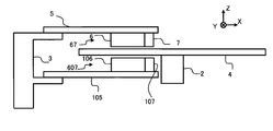
- FIG. 9 schematically shows another configuration of the near-field light defect inspection apparatus 1.
- This configuration has two sliders 67 and 607 for inspecting both surfaces of the wafer 4.
- the near-field light defect inspection apparatus 1 includes a suspension 5 on the positive side of the Z axis of the wafer 4 and a suspension 105 on the negative side of the Z axis.
- the suspension 5 supports the slider 67
- the suspension 105 supports the slider 607.
- the slider 67 has the configuration described in the first or second embodiment.
- the slider 607 has a slider body 106 and a laminated element unit 107.
- the slider 67 and the slider 607 are arranged so as to sandwich the wafer 4.
- the suspension 105 has the same configuration as the suspension 5, and the slider 607 may have the same configuration as the slider 67. These may have different configurations.
- the suspensions 5 and 105 are fixed to the moving support mechanism 3.
- the controller 52 can move and position the suspensions 5 and 105, that is, the sliders 67 and 607 on the wafer 4 at the same time by driving and controlling the movement support mechanism 3.
- the signal processing circuit 51 processes signals from the two sliders 67 and 607. By preparing the defect inspection sliders 67 and 607 on both surfaces of the wafer 4, both surfaces of the wafer can be inspected simultaneously, and the inspection time can be shortened.
- the suspensions 5 and 105 move simultaneously, and their relative positions are fixed in the XY plane. They are typically always in the same position in the XY plane. Unlike this, the movement support mechanism 3 may have a configuration in which the suspensions 5 and 105 are moved independently. During the defect inspection, the suspensions 5 and 105 may be in the same position or different positions in the XY plane.
- the configuration example of FIG. 9 has a plurality of sliders for defect inspection of different surfaces of the wafer 4, but unlike or in addition to this, the near-field optical defect inspection apparatus 1 simultaneously applies the same surface of the wafer 4 to the same surface.
- the slider for inspecting the same surface of the wafer 4 is positioned at different positions in the XY plane.
- the inspection time can be shortened by inspecting different regions on the wafer surface by the slider in the same plane. Also, the inspection accuracy can be increased by inspecting the same region by different sliders.
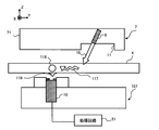
- FIG. 10 schematically shows another configuration of the near-field light defect inspection apparatus 1.
- This configuration example is different from the configuration example of FIG. 9 in the configuration of the laminated element portions 7 and 107 of the slider 67 and the slider 607.
- the condensing probe 90 is omitted in the laminated element unit 7 with respect to the laminated element unit described in the first and second embodiments, and the light emitting unit 8 is provided in the laminated element unit 107. It is omitted.
- the infrared light 16 from the light emitting unit 8 of the slider 67 is irradiated on the surface on the positive side of the Z-axis of the wafer 4 and propagates through the wafer 4 by repeating total reflection.
- the light (total reflection light) 117 propagating through the wafer 4 enters the defect 118, and near-field light 119 is generated.
- the light receiving unit 10 of the slider 607 collects the near-field light 119, converts it into an electrical signal, and transmits it to the controller 52.
- the inspection infrared light is irradiated from the slider on one surface of the wafer 4, and the near-field light due to the wafer internal defect is detected by the light receiving portion formed on the slider on the opposite surface.
- the structure of the (laminated element portion) can be made simpler and easier to manufacture.
- Various inventions can be formed by appropriately combining a plurality of constituent elements disclosed in the plurality of embodiments. For example, some components may be deleted from all the components shown in one embodiment. Furthermore, constituent elements over different embodiments may be appropriately combined.
- the present invention can be applied to the internal defect inspection of the object to be inspected having other shapes.
- the irradiation port for irradiating the inspection light is preferably formed in the slider, but may be arranged at another position.
Landscapes
- Physics & Mathematics (AREA)
- General Physics & Mathematics (AREA)
- Health & Medical Sciences (AREA)
- Life Sciences & Earth Sciences (AREA)
- Chemical & Material Sciences (AREA)
- Analytical Chemistry (AREA)
- Biochemistry (AREA)
- General Health & Medical Sciences (AREA)
- Immunology (AREA)
- Pathology (AREA)
- Investigating Materials By The Use Of Optical Means Adapted For Particular Applications (AREA)
- Testing Or Measuring Of Semiconductors Or The Like (AREA)
- Investigating Or Analysing Materials By Optical Means (AREA)
Abstract
Priority Applications (3)
| Application Number | Priority Date | Filing Date | Title |
|---|---|---|---|
| US14/118,851 US20140110606A1 (en) | 2011-05-27 | 2011-05-27 | Near-field optical defect inspection apparatus |
| PCT/JP2011/062203 WO2012164641A1 (fr) | 2011-05-27 | 2011-05-27 | Dispositif d'inspection de défauts optiques à champ proche |
| JP2013517708A JPWO2012164641A1 (ja) | 2011-05-27 | 2011-05-27 | 近接場光欠陥検査装置 |
Applications Claiming Priority (1)
| Application Number | Priority Date | Filing Date | Title |
|---|---|---|---|
| PCT/JP2011/062203 WO2012164641A1 (fr) | 2011-05-27 | 2011-05-27 | Dispositif d'inspection de défauts optiques à champ proche |
Publications (1)
| Publication Number | Publication Date |
|---|---|
| WO2012164641A1 true WO2012164641A1 (fr) | 2012-12-06 |
Family
ID=47258530
Family Applications (1)
| Application Number | Title | Priority Date | Filing Date |
|---|---|---|---|
| PCT/JP2011/062203 Ceased WO2012164641A1 (fr) | 2011-05-27 | 2011-05-27 | Dispositif d'inspection de défauts optiques à champ proche |
Country Status (3)
| Country | Link |
|---|---|
| US (1) | US20140110606A1 (fr) |
| JP (1) | JPWO2012164641A1 (fr) |
| WO (1) | WO2012164641A1 (fr) |
Cited By (1)
| Publication number | Priority date | Publication date | Assignee | Title |
|---|---|---|---|---|
| JP2019535023A (ja) * | 2016-09-28 | 2019-12-05 | ケーエルエー コーポレイション | 光近接場計測 |
Families Citing this family (5)
| Publication number | Priority date | Publication date | Assignee | Title |
|---|---|---|---|---|
| US9202488B2 (en) * | 2014-01-09 | 2015-12-01 | Seagate Technology Llc | Light blocker for stray light reduction within a slider |
| JP6426202B2 (ja) * | 2015-01-23 | 2018-11-21 | 京セラ株式会社 | 測定装置および測定方法 |
| US20170284943A1 (en) * | 2016-03-29 | 2017-10-05 | Nilanjan Ghosh | Detecting voids and delamination in photoresist layer |
| JP2019002725A (ja) * | 2017-06-13 | 2019-01-10 | コニカミノルタ株式会社 | 欠陥検査装置 |
| US10928329B2 (en) | 2017-10-11 | 2021-02-23 | Board Of Regents, The University Of Texas System | Method and system for optically detecting and characterizing defects in semiconductors |
Citations (10)
| Publication number | Priority date | Publication date | Assignee | Title |
|---|---|---|---|---|
| JPH10221268A (ja) * | 1997-02-05 | 1998-08-21 | Advantest Corp | ウェーハの表面状態検出方法および装置 |
| JP2000113503A (ja) * | 1998-10-08 | 2000-04-21 | Sharp Corp | 光記録媒体および光記憶装置 |
| JP2001283453A (ja) * | 2000-01-27 | 2001-10-12 | Tosoh Corp | 浮上式光記録再生ヘッド及びその浮上量制御方法 |
| JP2001305072A (ja) * | 2000-04-25 | 2001-10-31 | Advantest Corp | 基板の欠陥検出方法及び装置 |
| JP2002014028A (ja) * | 2000-06-30 | 2002-01-18 | Toshiba Corp | 近接場光検出光学系、近接場光学装置、およびそれらを用いた光学情報の検出方法 |
| JP2002122551A (ja) * | 2000-10-18 | 2002-04-26 | Kanagawa Acad Of Sci & Technol | 欠陥検出装置及び欠陥検出方法 |
| JP2005257339A (ja) * | 2004-03-09 | 2005-09-22 | Heureka Co Ltd | 半導体ウエハ検査装置 |
| JP2007298314A (ja) * | 2006-04-28 | 2007-11-15 | Univ Of Tokyo | 非破壊膜厚計測方法及び装置 |
| WO2009037972A1 (fr) * | 2007-09-19 | 2009-03-26 | Konica Minolta Opto, Inc. | Tête optique, tête d'enregistrement magnétique à assistance optique et dispositif d'enregistrement optique |
| JP2010286309A (ja) * | 2009-06-10 | 2010-12-24 | Toshiba Corp | ナノインプリント用テンプレートの検査方法 |
Family Cites Families (1)
| Publication number | Priority date | Publication date | Assignee | Title |
|---|---|---|---|---|
| JP2002122521A (ja) * | 2000-08-02 | 2002-04-26 | Univ Waseda | 建材・施工材からの揮発性有機化合物等の放散量検出装置 |
-
2011
- 2011-05-27 WO PCT/JP2011/062203 patent/WO2012164641A1/fr not_active Ceased
- 2011-05-27 US US14/118,851 patent/US20140110606A1/en not_active Abandoned
- 2011-05-27 JP JP2013517708A patent/JPWO2012164641A1/ja active Pending
Patent Citations (10)
| Publication number | Priority date | Publication date | Assignee | Title |
|---|---|---|---|---|
| JPH10221268A (ja) * | 1997-02-05 | 1998-08-21 | Advantest Corp | ウェーハの表面状態検出方法および装置 |
| JP2000113503A (ja) * | 1998-10-08 | 2000-04-21 | Sharp Corp | 光記録媒体および光記憶装置 |
| JP2001283453A (ja) * | 2000-01-27 | 2001-10-12 | Tosoh Corp | 浮上式光記録再生ヘッド及びその浮上量制御方法 |
| JP2001305072A (ja) * | 2000-04-25 | 2001-10-31 | Advantest Corp | 基板の欠陥検出方法及び装置 |
| JP2002014028A (ja) * | 2000-06-30 | 2002-01-18 | Toshiba Corp | 近接場光検出光学系、近接場光学装置、およびそれらを用いた光学情報の検出方法 |
| JP2002122551A (ja) * | 2000-10-18 | 2002-04-26 | Kanagawa Acad Of Sci & Technol | 欠陥検出装置及び欠陥検出方法 |
| JP2005257339A (ja) * | 2004-03-09 | 2005-09-22 | Heureka Co Ltd | 半導体ウエハ検査装置 |
| JP2007298314A (ja) * | 2006-04-28 | 2007-11-15 | Univ Of Tokyo | 非破壊膜厚計測方法及び装置 |
| WO2009037972A1 (fr) * | 2007-09-19 | 2009-03-26 | Konica Minolta Opto, Inc. | Tête optique, tête d'enregistrement magnétique à assistance optique et dispositif d'enregistrement optique |
| JP2010286309A (ja) * | 2009-06-10 | 2010-12-24 | Toshiba Corp | ナノインプリント用テンプレートの検査方法 |
Non-Patent Citations (2)
| Title |
|---|
| SATORU TAKAHASHI: "Kinsetsubako o Mochiita Handotai Wafer Hyomenseijo no Kobunkaino Hyoka", 2007 NENDO THE JAPAN SOCIETY FOR PRECISION ENGINEERING SHUKI TAIKAI SYMPOSIUM SHIRYO, 3 September 2007 (2007-09-03), pages 15 - 17 * |
| SATORU TAKAHASHI: "Surface Evaluation Technology Using Near-field Optics", JOURNAL OF THE JAPAN SOCIETY OF PRECISION ENGINEERING, vol. 73, no. 8, 5 August 2007 (2007-08-05), pages 883 - 887 * |
Cited By (2)
| Publication number | Priority date | Publication date | Assignee | Title |
|---|---|---|---|---|
| JP2019535023A (ja) * | 2016-09-28 | 2019-12-05 | ケーエルエー コーポレイション | 光近接場計測 |
| US11815347B2 (en) | 2016-09-28 | 2023-11-14 | Kla-Tencor Corporation | Optical near-field metrology |
Also Published As
| Publication number | Publication date |
|---|---|
| JPWO2012164641A1 (ja) | 2014-07-31 |
| US20140110606A1 (en) | 2014-04-24 |
Similar Documents
| Publication | Publication Date | Title |
|---|---|---|
| WO2012164641A1 (fr) | Dispositif d'inspection de défauts optiques à champ proche | |
| US7933169B2 (en) | Optical head for near-field recording and reproducing device | |
| US8656509B2 (en) | Scanning probe microscope and surface shape measuring method using same | |
| US8424111B2 (en) | Near-field optical microscope, near-field optical probe, and sample observation method | |
| US20080142733A1 (en) | Substrate processing apparatus and method | |
| US8713710B2 (en) | Cantilever of scanning probe microscope and method for manufacturing the same, method for inspecting thermal assist type magnetic head device and its apparatus | |
| KR102704604B1 (ko) | 결합파의 경로를 결정하기 위한 방법 및 측정 장치 | |
| JP2010514167A (ja) | 基板プロセス装置および方法 | |
| CN102401637B (zh) | 三维形状测量装置 | |
| JP2006323908A (ja) | ヘッドモジュール | |
| JP2005257339A (ja) | 半導体ウエハ検査装置 | |
| JP5154149B2 (ja) | 三次元測定プローブ | |
| TWI401674B (zh) | 飛行高度與滑動器突起測量之設備及系統 | |
| JP2019203705A (ja) | 形状測定用プローブ | |
| US8553512B2 (en) | Magnetic head slider inspection device | |
| US20170365497A1 (en) | Method and system for positioning using near field transducers, particularly suited for positioning electronic chips using interposers | |
| JP2014071927A (ja) | 熱アシスト磁気ヘッド検査方法及び熱アシスト磁気ヘッド検査装置 | |
| JP2008141207A (ja) | 故障解析装置 | |
| US10203353B2 (en) | Method and system for positioning using near field transducers, particularly suited for positioning electronic chips | |
| JP5969876B2 (ja) | 熱アシスト磁気ヘッド検査方法および熱アシスト磁気ヘッド検査装置 | |
| JP4394012B2 (ja) | ディスク検査装置 | |
| JP2006038774A (ja) | 近接場光評価装置 | |
| KR20250031881A (ko) | 웨이퍼 검사 장치 및 웨이퍼 검사 방법 | |
| JP5957352B2 (ja) | 熱アシスト磁気ヘッド検査方法および熱アシスト磁気ヘッド検査装置 | |
| JP4482254B2 (ja) | 光ヘッド |
Legal Events
| Date | Code | Title | Description |
|---|---|---|---|
| 121 | Ep: the epo has been informed by wipo that ep was designated in this application |
Ref document number: 11866982 Country of ref document: EP Kind code of ref document: A1 |
|
| ENP | Entry into the national phase |
Ref document number: 2013517708 Country of ref document: JP Kind code of ref document: A |
|
| WWE | Wipo information: entry into national phase |
Ref document number: 14118851 Country of ref document: US |
|
| NENP | Non-entry into the national phase |
Ref country code: DE |
|
| 122 | Ep: pct application non-entry in european phase |
Ref document number: 11866982 Country of ref document: EP Kind code of ref document: A1 |