WO2012164822A1 - Procédé de fabrication de tranche liée, et tranche de silicium sur isolant (soi) liée - Google Patents
Procédé de fabrication de tranche liée, et tranche de silicium sur isolant (soi) liée Download PDFInfo
- Publication number
- WO2012164822A1 WO2012164822A1 PCT/JP2012/002835 JP2012002835W WO2012164822A1 WO 2012164822 A1 WO2012164822 A1 WO 2012164822A1 JP 2012002835 W JP2012002835 W JP 2012002835W WO 2012164822 A1 WO2012164822 A1 WO 2012164822A1
- Authority
- WO
- WIPO (PCT)
- Prior art keywords
- wafer
- ion implantation
- bonded
- ion
- manufacturing
- Prior art date
- Legal status (The legal status is an assumption and is not a legal conclusion. Google has not performed a legal analysis and makes no representation as to the accuracy of the status listed.)
- Ceased
Links
Images


Classifications
-
- H—ELECTRICITY
- H10—SEMICONDUCTOR DEVICES; ELECTRIC SOLID-STATE DEVICES NOT OTHERWISE PROVIDED FOR
- H10P—GENERIC PROCESSES OR APPARATUS FOR THE MANUFACTURE OR TREATMENT OF DEVICES COVERED BY CLASS H10
- H10P30/00—Ion implantation into wafers, substrates or parts of devices
- H10P30/20—Ion implantation into wafers, substrates or parts of devices into semiconductor materials, e.g. for doping
- H10P30/222—Ion implantation into wafers, substrates or parts of devices into semiconductor materials, e.g. for doping characterised by the angle between the ion beam and the crystal planes or the main crystal surface
-
- H—ELECTRICITY
- H10—SEMICONDUCTOR DEVICES; ELECTRIC SOLID-STATE DEVICES NOT OTHERWISE PROVIDED FOR
- H10D—INORGANIC ELECTRIC SEMICONDUCTOR DEVICES
- H10D86/00—Integrated devices formed in or on insulating or conducting substrates, e.g. formed in silicon-on-insulator [SOI] substrates or on stainless steel or glass substrates
-
- H—ELECTRICITY
- H10—SEMICONDUCTOR DEVICES; ELECTRIC SOLID-STATE DEVICES NOT OTHERWISE PROVIDED FOR
- H10D—INORGANIC ELECTRIC SEMICONDUCTOR DEVICES
- H10D62/00—Semiconductor bodies, or regions thereof, of devices having potential barriers
-
- H—ELECTRICITY
- H10—SEMICONDUCTOR DEVICES; ELECTRIC SOLID-STATE DEVICES NOT OTHERWISE PROVIDED FOR
- H10D—INORGANIC ELECTRIC SEMICONDUCTOR DEVICES
- H10D62/00—Semiconductor bodies, or regions thereof, of devices having potential barriers
- H10D62/01—Manufacture or treatment
-
- H—ELECTRICITY
- H10—SEMICONDUCTOR DEVICES; ELECTRIC SOLID-STATE DEVICES NOT OTHERWISE PROVIDED FOR
- H10P—GENERIC PROCESSES OR APPARATUS FOR THE MANUFACTURE OR TREATMENT OF DEVICES COVERED BY CLASS H10
- H10P30/00—Ion implantation into wafers, substrates or parts of devices
- H10P30/20—Ion implantation into wafers, substrates or parts of devices into semiconductor materials, e.g. for doping
-
- H—ELECTRICITY
- H10—SEMICONDUCTOR DEVICES; ELECTRIC SOLID-STATE DEVICES NOT OTHERWISE PROVIDED FOR
- H10P—GENERIC PROCESSES OR APPARATUS FOR THE MANUFACTURE OR TREATMENT OF DEVICES COVERED BY CLASS H10
- H10P72/00—Handling or holding of wafers, substrates or devices during manufacture or treatment thereof
- H10P72/70—Handling or holding of wafers, substrates or devices during manufacture or treatment thereof for supporting or gripping
- H10P72/76—Handling or holding of wafers, substrates or devices during manufacture or treatment thereof for supporting or gripping using mechanical means, e.g. clamps or pinches
- H10P72/7604—Handling or holding of wafers, substrates or devices during manufacture or treatment thereof for supporting or gripping using mechanical means, e.g. clamps or pinches the wafers being placed on a susceptor, stage or support
- H10P72/7618—Handling or holding of wafers, substrates or devices during manufacture or treatment thereof for supporting or gripping using mechanical means, e.g. clamps or pinches the wafers being placed on a susceptor, stage or support characterised by a movable susceptor, stage or support, others than those only rotating on their own vertical axis, e.g. susceptors on a rotating carrousel
-
- H—ELECTRICITY
- H10—SEMICONDUCTOR DEVICES; ELECTRIC SOLID-STATE DEVICES NOT OTHERWISE PROVIDED FOR
- H10P—GENERIC PROCESSES OR APPARATUS FOR THE MANUFACTURE OR TREATMENT OF DEVICES COVERED BY CLASS H10
- H10P72/00—Handling or holding of wafers, substrates or devices during manufacture or treatment thereof
- H10P72/70—Handling or holding of wafers, substrates or devices during manufacture or treatment thereof for supporting or gripping
- H10P72/76—Handling or holding of wafers, substrates or devices during manufacture or treatment thereof for supporting or gripping using mechanical means, e.g. clamps or pinches
- H10P72/7604—Handling or holding of wafers, substrates or devices during manufacture or treatment thereof for supporting or gripping using mechanical means, e.g. clamps or pinches the wafers being placed on a susceptor, stage or support
- H10P72/7621—Handling or holding of wafers, substrates or devices during manufacture or treatment thereof for supporting or gripping using mechanical means, e.g. clamps or pinches the wafers being placed on a susceptor, stage or support characterised by supporting two or more semiconductor substrates
-
- H—ELECTRICITY
- H10—SEMICONDUCTOR DEVICES; ELECTRIC SOLID-STATE DEVICES NOT OTHERWISE PROVIDED FOR
- H10P—GENERIC PROCESSES OR APPARATUS FOR THE MANUFACTURE OR TREATMENT OF DEVICES COVERED BY CLASS H10
- H10P90/00—Preparation of wafers not covered by a single main group of this subclass, e.g. wafer reinforcement
- H10P90/19—Preparing inhomogeneous wafers
- H10P90/1904—Preparing vertically inhomogeneous wafers
- H10P90/1906—Preparing SOI wafers
- H10P90/1914—Preparing SOI wafers using bonding
- H10P90/1916—Preparing SOI wafers using bonding with separation or delamination along an ion implanted layer, e.g. Smart-cut
-
- H—ELECTRICITY
- H10—SEMICONDUCTOR DEVICES; ELECTRIC SOLID-STATE DEVICES NOT OTHERWISE PROVIDED FOR
- H10W—GENERIC PACKAGES, INTERCONNECTIONS, CONNECTORS OR OTHER CONSTRUCTIONAL DETAILS OF DEVICES COVERED BY CLASS H10
- H10W10/00—Isolation regions in semiconductor bodies between components of integrated devices
- H10W10/10—Isolation regions comprising dielectric materials
- H10W10/181—Semiconductor-on-insulator [SOI] isolation regions, e.g. buried oxide regions of SOI wafers
-
- Y—GENERAL TAGGING OF NEW TECHNOLOGICAL DEVELOPMENTS; GENERAL TAGGING OF CROSS-SECTIONAL TECHNOLOGIES SPANNING OVER SEVERAL SECTIONS OF THE IPC; TECHNICAL SUBJECTS COVERED BY FORMER USPC CROSS-REFERENCE ART COLLECTIONS [XRACs] AND DIGESTS
- Y10—TECHNICAL SUBJECTS COVERED BY FORMER USPC
- Y10S—TECHNICAL SUBJECTS COVERED BY FORMER USPC CROSS-REFERENCE ART COLLECTIONS [XRACs] AND DIGESTS
- Y10S438/00—Semiconductor device manufacturing: process
- Y10S438/977—Thinning or removal of substrate
Definitions
- the present invention relates to a method for manufacturing a bonded wafer using an ion implantation separation method, and in particular, a silicon single crystal wafer into which hydrogen ions or the like are implanted is bonded to a base wafer serving as a support substrate, and then peeled and bonded to the bonded wafer. It relates to a method of manufacturing.
- ion-implantation separation method a technique also called Smart Cut Method (registered trademark)
- an oxide film is formed on at least one of two wafers, and gas ions such as hydrogen ions and rare gas ions are implanted from the upper surface of one wafer (bond wafer).
- polishing polish in order to remove the damaged layer and the like, mirror polishing (removal allowance: about 100 nm) called “polishing polish” has been performed in the final step after the bonding heat treatment.
- polishing allowance is not uniform. Therefore, the film thickness uniformity achieved to some extent by implantation and peeling of hydrogen ions and the like is achieved. The problem of getting worse arises.
- a flattening process for improving the surface roughness by performing a high-temperature heat treatment instead of the touch polish has been performed.
- a heat treatment under a reducing atmosphere containing hydrogen rapid heating / rapid cooling heat treatment (RTA treatment)
- RTA treatment rapid cooling heat treatment
- the SOI wafer after peeling is subjected to sacrificial oxidation treatment after planarization heat treatment in an inert gas, hydrogen gas, or mixed gas atmosphere thereof, thereby planarizing the peeled surface and OSF. Achieving avoidance simultaneously.
- a flattening process for improving the surface roughness by performing a high-temperature heat treatment instead of the touch polish is performed, and at present, the film thickness range of the SOI layer with a diameter of 300 mm (maximum in the plane).
- An SOI wafer having a film thickness uniformity of 3 nm or less (a value obtained by subtracting the minimum film thickness value from the film thickness value) is obtained at the mass production level by the ion implantation delamination method.
- the ion implantation depth (range) distribution is directly reflected in the film thickness distribution of the thin film after the separation.
- a cone angle effect is known.
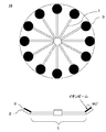
- the batch type ion implanter includes a rotating body 1 and a plurality of wafer holders 2 provided on the rotating body 1 and on which a substrate 3 is arranged.
- the wafer holder 2 is slightly inclined inward from the rotating surface of the rotating body 1.
- the second cause of film thickness distribution is that channeling occurs in the fabrication of a Thin BOX type SOI wafer or a directly bonded wafer without an oxide film.
- a direct bonding wafer without an oxide film and a Thin BOX type SOI wafer having a BOX layer (silicon oxide film layer) thickness of 100 nm or less the effect of scattering by the oxide film becomes weak and the implantation angle is set to 0 degree. In the ion implantation, channeling occurs.
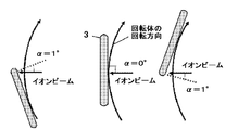
- the crystal plane and the angle of the ion beam are perpendicular to the center of the substrate, so that the effect of channeling is increased and the ion implantation depth is increased.
- the implantation angle is caused by the cone angle at both ends of the substrate in the scanning direction, the influence of channeling becomes relatively weak and the ion implantation depth becomes shallow (see FIG. 6).
- the effect of cone angle is particularly emphasized by channeling.
- a method is generally known in which the implantation angle is inclined with respect to the crystal plane.
- the effect of the cone angle differs between the two ends of the substrate in the scanning direction.
- In-plane depth distribution increases.
- a method for preventing channeling by using a wafer (wafer with an off-angle) whose crystal axis direction is tilted is known. Like the method of tilting the implantation angle, implantation is performed between both ends in the scanning direction. Since the angles are different, the in-plane depth distribution becomes large.
- the present invention has been made in view of the above problems, and is capable of manufacturing a bonded wafer with improved film thickness uniformity of a thin film on a base wafer, particularly an SOI layer, at a mass production level. It aims at providing the manufacturing method of.
- the present invention includes a rotating body and a plurality of wafer holders provided on the rotating body and arranged on the substrate, and ion implantation is performed on the plurality of substrates arranged and revolved on the wafer holder.
- a bonded wafer having a thin film on the base wafer is manufactured by bonding the bonded surface and the surface of the base wafer directly or through an insulating film, and peeling the bond wafer with the ion-implanted layer.
- the ion implantation into the bond wafer in the ion implantation process is performed in a plurality of times, and after each ion implantation, the bond wafer disposed on the wafer holder is rotated by a predetermined rotation angle and rotated.
- a method for manufacturing a bonded wafer wherein the next ion implantation is performed at a position.
- the ion implantation into the bond wafer in the ion implantation process using the batch type ion implanter is performed in a plurality of times, and the wafer is held after each ion implantation.
- the bond wafer By rotating the bond wafer placed on the tool by a predetermined rotation angle and performing the next ion implantation at the rotated placement position, the bond wafer can be loaded into the wafer holder in a different direction for each ion implantation.
- the dispersion of ion implantation depth distribution is improved, and finally, bonded wafers with dramatically improved thin film thickness uniformity are manufactured at the mass production level. can do.
- the ion implantation is performed in two steps, and after the first ion implantation, the bond wafer is rotated 90 degrees or 180 degrees, and the second ion implantation is performed at the rotated arrangement position. Is preferred.
- the bond wafer is rotated 180 degrees, and the second ion implantation is performed at the rotated arrangement position, so that the crystal axis orientation of the bond wafer to be used is shifted due to the influence of processing accuracy or the like. Even in such a case, it is possible to cancel the influence of the deviation of the crystal axis, and finally, it is possible to manufacture a bonded wafer in which the film thickness uniformity of the thin film is drastically improved at a mass production level.
- the ion implantation is performed in four steps, and the second and subsequent ion implantations are rotated by any rotation angle of 90, 180, or 270 degrees with respect to the first ion implantation. Preferably it is done in position.
- the variation can be further reduced as compared with the case in which the ion implantation is performed in two times, and the ion implantation depth distribution becomes closer to a concentric distribution.
- the correction of the film thickness distribution by this process becomes even easier.
- the ion implantation is performed each time by setting the angle between the crystal plane of the surface of the bond wafer and the ion implantation direction to be vertical.
- the angle between the crystal plane of the bond wafer surface and the ion implantation direction perpendicular that is, by setting the ion implantation angle to 0 degrees, the variation in the film thickness distribution of the thin film after peeling is further suppressed. This is preferable.
- the bond wafer it is preferable that a silicon single crystal wafer is used as the bond wafer and the insulating film is a silicon oxide film having a thickness of 100 nm or less.
- the in-plane film thickness range is 1 nm.
- a thin film SOI wafer having the following extremely good film thickness uniformity can be manufactured.
- the thin film on the base wafer is subjected to sacrificial oxidation treatment, and the thin film is formed using an oxidation furnace in which the oxide film thickness distribution formed by the sacrificial oxidation is concentric and the outer peripheral oxide film thickness is reduced. It is preferable to adjust the film thickness of the thin film by performing a sacrificial oxidation treatment.
- the sacrificial oxidation process is further performed on the thin film on the base wafer after the peeling process by using an oxidation furnace in which the formed oxide film thickness distribution is concentric and the outer peripheral oxide film thickness is reduced.
- the film thickness of the thin film can be adjusted, and a bonded wafer having a further improved film thickness range than immediately after peeling can be obtained.
- a Thin BOX type thin film SOI wafer having a silicon oxide film of 100 nm or less has conventionally been difficult to obtain good film thickness uniformity.
- the method for manufacturing a bonded wafer according to the present invention uses the bonded SOI wafer in which the buried oxide film layer and the SOI layer are sequentially formed on the surface of the base wafer, and the film of the buried oxide film layer.
- a bonded SOI wafer is provided in which the thickness is 100 nm or less, and the in-plane film thickness range of the SOI layer is 1 nm or less.
- the dispersion of the ion implantation depth distribution can be improved, and finally the bonded wafer whose film thickness uniformity has been dramatically improved can be obtained. Since it can be manufactured at a mass production level, the threshold voltage of a device using such a bonded wafer can be stabilized, and the device yield is improved.
- FIG. 4 is an SOI layer film thickness distribution immediately after peeling in Example 1.
- FIG. 4 is an SOI layer film thickness distribution immediately after peeling in Example 2.
- FIG. It is SOI layer film thickness distribution immediately after peeling in a comparative example.
- the present inventors shall perform the ion implantation into the bond wafer in the ion implantation step in a plurality of times, and after each ion implantation, the bond wafer is rotated by a predetermined rotation angle, and at the rotated arrangement position, the next position is rotated.
- ion implantation it was found that variations in the thin film distribution on the base wafer, particularly the SOI film thickness, caused by the cone angle effect can be suppressed by avoiding ion implantation at overlapping positions, and the present invention was completed. I let you. The present invention will be described in detail below.
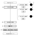
- FIG. 1 is a process flow diagram showing an example of a method for producing a bonded wafer according to the present invention.
- the present invention provides a batch type ion implanter that includes a rotating body and a plurality of wafer holders that are provided on the rotating body and that disposes a substrate, and that performs ion implantation on a plurality of substrates that are disposed and revolved on the wafer holder.
- An ion implantation step (FIG. 1A) for forming an ion implantation layer by implanting at least one kind of gas ions of hydrogen ions and rare gas ions from the surface of the bond wafer; and ion implantation of the bond wafer
- a bonding step (FIG.
- At least one kind of gas ion of hydrogen ion or rare gas ion is ion-implanted from the surface of the bond wafer to form an ion-implanted layer.
- hydrogen molecular ions are also included in “hydrogen ions”.
- the bond wafer to be ion-implanted can be arbitrarily selected according to the purpose and is not particularly limited. For example, if a silicon single crystal wafer is used, the SOI film having a very uniform film thickness is used. SOI wafers with layers can be manufactured. Moreover, it is preferable to form an insulating film in advance on the surface of the bond wafer before ion implantation.
- the bond wafer has a diameter of 300 mm or more where the cone angle effect is noticeable. Even if the silicon single crystal wafer is used and the insulating film is a silicon oxide film having a thickness of 100 nm or less or 50 nm or less, a Thin BOX type thin film SOI wafer having excellent film thickness uniformity can be manufactured.
- the batch type ion implanter 10 includes a rotating body 1 and a plurality of wafer holders 2 provided on the rotating body 1 and on which a substrate 3 is arranged, and a plurality of substrates 3 arranged and revolved on the wafer holder 2. Ion implantation.
- ion implantation into the bond wafer 3 in the ion implantation step is performed in a plurality of times, and after each ion implantation, The bond wafer 3 disposed on the wafer holder 2 is rotated by a predetermined rotation angle, and the next ion implantation is performed at the rotated position.
- FIG. 1A shows an example in which ion implantation is performed n times (n ⁇ 2). After the first ion implantation, the bond wafer 3 is rotated 90 ° (notch 3 ′ position is 90 °), and the second ion implantation is performed at the rotated arrangement position.
- the ion implantation depth distribution generated between the wafer central portion and both end portions of the wafer in the scanning direction of the implanted ion beam due to the cone angle effect causes a two-fold symmetrical ion implantation depth distribution.
- ion implantation is performed in two steps, and if the wafer is rotated 90 degrees between each ion implantation, the ion implantation depth is relatively deep at the center of the bond wafer.
- the outer peripheral portion becomes shallow all around and becomes a uniform distribution, which is close to a concentric distribution.
- the oxide film thickness distribution and the polishing allowance distribution are concentric distributions. For this reason, variation in film thickness distribution due to ion implantation is improved, and if it becomes a concentric distribution, the film thickness distribution can be easily corrected by processing such as oxidation performed in the bonded wafer manufacturing process. The film thickness distribution of the thin film obtained can be improved.
- the ion implantation is not limited to two times, and ion implantation is performed in four times, and the second and subsequent ion implantations are performed at any rotation angle of 90, 180, and 270 degrees with respect to the first ion implantation.
- the distribution of concentric circles is more uniform than in the case of double injection by performing the rotation at the position where only the rotation is performed. For this reason, the correction of the film thickness distribution by the treatment such as oxidation becomes easier.
- the crystal axis orientation of the bond wafer to be used is slightly shifted due to the influence of processing accuracy, even if the implantation angle is set to 0 degrees with respect to the wafer surface, the crystal axis and the ion beam actually have an angle. . For this reason, since the two-fold symmetrical distribution in the scanning direction is broken, the depth distribution of concentric circles may not be obtained by the two-fold divided injection. In this case, if the wafer orientation of the two-time split implantation is set to 180 degrees, the crystal axis deviation can be canceled out, resulting in a concentric distribution, and finally mass production of bonded wafers with improved thin film thickness uniformity. Can be manufactured at level.
- the influence of the crystal axis shift can be further suppressed by setting the angle for canceling the crystal axis shift to the ion beam implantation angle. That is, by making the angle between the crystal plane of the bond wafer surface and the ion implantation direction perpendicular (setting the ion implantation angle with respect to the crystal plane to 0 degree), the variation in the film thickness distribution of the thin film after the peeling process is reduced. Further, it can be suppressed, which is preferable.
- the bond wafer cleaning process is performed between the ion implantations, the particles adhering to the ion implantation surface are removed, so that an obstacle to the ion implantation can be eliminated.
- the ion-implanted surface of the bond wafer and the surface of the base wafer are bonded directly or through an insulating film.
- a silicon single crystal wafer can be used as the base wafer, but is not particularly limited. Normally, the wafers are bonded to each other without using an adhesive or the like by bringing the surfaces of the bond wafer and the base wafer into contact with each other in a clean atmosphere at room temperature.
- the bonded wafer having the thin film on the base wafer is manufactured by peeling the bond wafer with the ion implantation layer.
- the bond wafer can be peeled off by the ion implantation layer.
- plasma treatment on the bonding surface at room temperature in advance, it is possible to perform peeling by applying external force without performing heat treatment (or after performing heat treatment not to peel).
- the thin film immediately after such a peeling step has a large diameter of 300 mm or 450 mm, and even if it is a Thin BOX type with an insulating film of 100 nm or less, the film thickness range is 1 nm or less.
- the film thickness distribution becomes close to a concentric circle, and the film thickness distribution can be easily corrected by subsequent thinning by oxidation or polishing.
- sacrificial oxidation treatment thermal oxidation + oxide film removal
- reducing atmosphere or non-reducing atmosphere are used to improve the bond strength, adjust the thickness of the thin film, and planarize the surface of the thin film.
- a bonded wafer by performing a heat treatment in an active gas atmosphere.
- the oxidation furnace that performs the oxidation treatment uses an oxidation furnace in which the oxide film thickness distribution formed by sacrificial oxidation is concentric and the outer peripheral oxide film thickness is reduced, so that the film thickness is further increased immediately after peeling.
- a bonded wafer having an improved range and excellent film thickness uniformity can be manufactured.
- each step after the stripping step sacrificial oxidation treatment, reducing atmosphere heat treatment, etc.
- the stock allowance distribution of the thin film deviates from the concentric shape
- the final thin film thickness distribution is improved.
- the implantation angle at the time of each ion implantation can be finely adjusted.
- Example 1 A thermal oxide film serving as a BOX layer (buried oxide film layer) is formed to a thickness of 25 nm on a bond wafer made of a silicon single crystal having a diameter of 300 mm and a crystal orientation ⁇ 100> (the crystal plane of the surface is (100) just and there is no angular deviation) Thereafter, hydrogen ion implantation was performed using a batch type ion implanter as shown in FIG. Hydrogen ion implantation is performed in two steps, and the first ion implantation is performed under the conditions of H + , 30 keV, 2.6e16 cm ⁇ 2 , implantation angle 0 degree, and notch orientation angle 0 degree.
- the notch orientation angle is an angle obtained by rotating the notch position of the wafer clockwise from the standard position (0 degree) when the bond wafer is placed on the wafer holder of the ion implantation apparatus.
- the vertical thermal oxidation furnace that has undergone oxidation treatment is a type that performs oxidation treatment while rotating the wafer boat that holds the wafer, and the in-plane distribution of the thermal oxide film thickness that is formed is extremely good.
- the distribution shape tends to be concentric and the oxide film thickness on the wafer outer peripheral side tends to be thin.
- the thickness range of the manufactured SOI layer was measured twice using Acumap manufactured by ADE, immediately after peeling, and after sacrificial oxidation treatment and heat treatment in a reducing atmosphere (after thinning).
- Table 1 shows the manufacturing conditions of the manufactured SOI wafer and the measurement results of the film thickness range (immediately after peeling and after thinning) of the SOI layer.
- Example 2 Except for the ion implantation step, an SOI wafer was manufactured in the same manner as in Example 1. Hydrogen ion implantation is performed in four steps, and the first ion implantation is performed under the conditions of H + , 30 keV, 1.3e16 cm ⁇ 2 , implantation angle 0 degree, and notch orientation angle 0 degree.
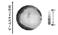
- Table 1 shows the manufacturing conditions of the manufactured SOI wafer and the measurement results of the film thickness range (immediately after peeling and after thinning) of the SOI layer. Further, FIG. 5 shows the SOI film thickness distribution immediately after peeling.
- the film thickness range of the SOI layer immediately after peeling was smaller than the target value of 1 nm in Examples 1 and 2. Furthermore, the shape of the distribution was close to a concentric shape. On the other hand, in the case of the comparative example, the film thickness range of the SOI layer immediately after peeling exceeded 1 nm, and the distribution shape was a two-fold symmetrical shape. Moreover, the film thickness range after completion of the sacrificial oxidation treatment and the reducing atmosphere heat treatment in Examples 1 and 2 was further improved as compared with that immediately after peeling.
- the bonded SOI wafer manufactured in Examples 1 and 2 is a Thin BOX type having a diameter of 300 mm and a BOX layer of 25 nm
- the in-plane film thickness range of the SOI layer is 1 nm immediately after peeling. Furthermore, it is maintained at 1 nm or less even after the treatment of improving the bonding strength, adjusting the thickness of the SOI layer, and planarizing the surface of the SOI layer, and is an extremely good surface that could not be obtained by the conventional manufacturing method.
- a bonded SOI wafer having an inner film thickness range was obtained.
- the present invention is not limited to the above embodiment.
- the above-described embodiment is an exemplification, and the present invention has any configuration that has substantially the same configuration as the technical idea described in the claims of the present invention and exhibits the same function and effect. Are included in the technical scope.
Landscapes
- Element Separation (AREA)
- Chemical & Material Sciences (AREA)
- Crystallography & Structural Chemistry (AREA)
Abstract
Priority Applications (4)
| Application Number | Priority Date | Filing Date | Title |
|---|---|---|---|
| KR1020137031854A KR101781812B1 (ko) | 2011-05-30 | 2012-04-25 | 접합 웨이퍼의 제조 방법 및 접합 soi 웨이퍼 |
| US14/114,959 US8987109B2 (en) | 2011-05-30 | 2012-04-25 | Method for manufacturing bonded wafer and bonded SOI wafer |
| CN201280026001.2A CN103563049B (zh) | 2011-05-30 | 2012-04-25 | 贴合晶片的制造方法 |
| EP12792204.5A EP2717294B1 (fr) | 2011-05-30 | 2012-04-25 | Procédé de fabrication de tranche liée de silicium sur isolant (soi) |
Applications Claiming Priority (2)
| Application Number | Priority Date | Filing Date | Title |
|---|---|---|---|
| JP2011-120340 | 2011-05-30 | ||
| JP2011120340A JP5802436B2 (ja) | 2011-05-30 | 2011-05-30 | 貼り合わせウェーハの製造方法 |
Publications (1)
| Publication Number | Publication Date |
|---|---|
| WO2012164822A1 true WO2012164822A1 (fr) | 2012-12-06 |
Family
ID=47258700
Family Applications (1)
| Application Number | Title | Priority Date | Filing Date |
|---|---|---|---|
| PCT/JP2012/002835 Ceased WO2012164822A1 (fr) | 2011-05-30 | 2012-04-25 | Procédé de fabrication de tranche liée, et tranche de silicium sur isolant (soi) liée |
Country Status (6)
| Country | Link |
|---|---|
| US (1) | US8987109B2 (fr) |
| EP (1) | EP2717294B1 (fr) |
| JP (1) | JP5802436B2 (fr) |
| KR (1) | KR101781812B1 (fr) |
| CN (1) | CN103563049B (fr) |
| WO (1) | WO2012164822A1 (fr) |
Cited By (2)
| Publication number | Priority date | Publication date | Assignee | Title |
|---|---|---|---|---|
| WO2013088636A1 (fr) * | 2011-12-15 | 2013-06-20 | 信越半導体株式会社 | Procédé de fabrication de plaquette silicium sur isolant |
| JP2014154868A (ja) * | 2013-02-14 | 2014-08-25 | Ricoh Co Ltd | 強誘電体膜の成膜方法および製造装置 |
Families Citing this family (5)
| Publication number | Priority date | Publication date | Assignee | Title |
|---|---|---|---|---|
| FR3007891B1 (fr) | 2013-06-28 | 2016-11-25 | Soitec Silicon On Insulator | Procede de fabrication d'une structure composite |
| JP6213046B2 (ja) * | 2013-08-21 | 2017-10-18 | 信越半導体株式会社 | 貼り合わせウェーハの製造方法 |
| FR3063176A1 (fr) * | 2017-02-17 | 2018-08-24 | Soitec | Masquage d'une zone au bord d'un substrat donneur lors d'une etape d'implantation ionique |
| JP6686962B2 (ja) | 2017-04-25 | 2020-04-22 | 信越半導体株式会社 | 貼り合わせウェーハの製造方法 |
| CN109742023A (zh) * | 2018-11-27 | 2019-05-10 | 上海新傲科技股份有限公司 | 晶圆表面的平坦化方法 |
Citations (9)
| Publication number | Priority date | Publication date | Assignee | Title |
|---|---|---|---|---|
| JPH05211128A (ja) | 1991-09-18 | 1993-08-20 | Commiss Energ Atom | 薄い半導体材料フィルムの製造方法 |
| JPH11307472A (ja) | 1998-04-23 | 1999-11-05 | Shin Etsu Handotai Co Ltd | 水素イオン剥離法によってsoiウエーハを製造する方法およびこの方法で製造されたsoiウエーハ |
| JP2000124092A (ja) | 1998-10-16 | 2000-04-28 | Shin Etsu Handotai Co Ltd | 水素イオン注入剥離法によってsoiウエーハを製造する方法およびこの方法で製造されたsoiウエーハ |
| WO2001093334A1 (fr) * | 2000-05-30 | 2001-12-06 | Shin-Etsu Handotai Co.,Ltd. | Procede de fabrication d'une plaquette collee et cette derniere |
| WO2003009386A1 (fr) | 2001-07-17 | 2003-01-30 | Shin-Etsu Handotai Co.,Ltd. | Procede de production de plaquettes de liaison |
| JP2006324051A (ja) * | 2005-05-17 | 2006-11-30 | Nissin Ion Equipment Co Ltd | 荷電粒子ビーム照射方法および装置 |
| JP2007242972A (ja) * | 2006-03-09 | 2007-09-20 | Shin Etsu Handotai Co Ltd | Soiウェーハの製造方法 |
| JP2008182192A (ja) * | 2006-12-26 | 2008-08-07 | Sumco Corp | 貼り合わせウェーハの製造方法 |
| JP2010129839A (ja) * | 2008-11-28 | 2010-06-10 | Sumco Corp | 貼り合わせウェーハの製造方法 |
Family Cites Families (11)
| Publication number | Priority date | Publication date | Assignee | Title |
|---|---|---|---|---|
| JPH10125880A (ja) * | 1996-10-18 | 1998-05-15 | Sony Corp | 張り合わせsoi基板の作製方法 |
| US6458723B1 (en) * | 1999-06-24 | 2002-10-01 | Silicon Genesis Corporation | High temperature implant apparatus |
| JP3975634B2 (ja) * | 2000-01-25 | 2007-09-12 | 信越半導体株式会社 | 半導体ウェハの製作法 |
| GB0002669D0 (en) * | 2000-02-04 | 2000-03-29 | Applied Materials Inc | A method and apparatus for implanting semiconductor wafer substrates |
| US20040251539A1 (en) * | 2001-09-12 | 2004-12-16 | Faris Sadeg M. | Thermoelectric cooler array |
| JPWO2003046993A1 (ja) * | 2001-11-29 | 2005-04-14 | 信越半導体株式会社 | Soiウェーハの製造方法 |
| US7452757B2 (en) * | 2002-05-07 | 2008-11-18 | Asm America, Inc. | Silicon-on-insulator structures and methods |
| JP4407127B2 (ja) * | 2003-01-10 | 2010-02-03 | 信越半導体株式会社 | Soiウエーハの製造方法 |
| JP5020547B2 (ja) | 2006-06-02 | 2012-09-05 | 株式会社Sen | ビーム処理装置及びビーム処理方法 |
| US7687786B2 (en) * | 2008-05-16 | 2010-03-30 | Twin Creeks Technologies, Inc. | Ion implanter for noncircular wafers |
| JP2010040593A (ja) | 2008-07-31 | 2010-02-18 | Sumco Corp | イオン注入装置及び方法 |
-
2011
- 2011-05-30 JP JP2011120340A patent/JP5802436B2/ja active Active
-
2012
- 2012-04-25 CN CN201280026001.2A patent/CN103563049B/zh active Active
- 2012-04-25 US US14/114,959 patent/US8987109B2/en active Active
- 2012-04-25 EP EP12792204.5A patent/EP2717294B1/fr active Active
- 2012-04-25 WO PCT/JP2012/002835 patent/WO2012164822A1/fr not_active Ceased
- 2012-04-25 KR KR1020137031854A patent/KR101781812B1/ko active Active
Patent Citations (9)
| Publication number | Priority date | Publication date | Assignee | Title |
|---|---|---|---|---|
| JPH05211128A (ja) | 1991-09-18 | 1993-08-20 | Commiss Energ Atom | 薄い半導体材料フィルムの製造方法 |
| JPH11307472A (ja) | 1998-04-23 | 1999-11-05 | Shin Etsu Handotai Co Ltd | 水素イオン剥離法によってsoiウエーハを製造する方法およびこの方法で製造されたsoiウエーハ |
| JP2000124092A (ja) | 1998-10-16 | 2000-04-28 | Shin Etsu Handotai Co Ltd | 水素イオン注入剥離法によってsoiウエーハを製造する方法およびこの方法で製造されたsoiウエーハ |
| WO2001093334A1 (fr) * | 2000-05-30 | 2001-12-06 | Shin-Etsu Handotai Co.,Ltd. | Procede de fabrication d'une plaquette collee et cette derniere |
| WO2003009386A1 (fr) | 2001-07-17 | 2003-01-30 | Shin-Etsu Handotai Co.,Ltd. | Procede de production de plaquettes de liaison |
| JP2006324051A (ja) * | 2005-05-17 | 2006-11-30 | Nissin Ion Equipment Co Ltd | 荷電粒子ビーム照射方法および装置 |
| JP2007242972A (ja) * | 2006-03-09 | 2007-09-20 | Shin Etsu Handotai Co Ltd | Soiウェーハの製造方法 |
| JP2008182192A (ja) * | 2006-12-26 | 2008-08-07 | Sumco Corp | 貼り合わせウェーハの製造方法 |
| JP2010129839A (ja) * | 2008-11-28 | 2010-06-10 | Sumco Corp | 貼り合わせウェーハの製造方法 |
Non-Patent Citations (1)
| Title |
|---|
| See also references of EP2717294A4 |
Cited By (3)
| Publication number | Priority date | Publication date | Assignee | Title |
|---|---|---|---|---|
| WO2013088636A1 (fr) * | 2011-12-15 | 2013-06-20 | 信越半導体株式会社 | Procédé de fabrication de plaquette silicium sur isolant |
| US9240344B2 (en) | 2011-12-15 | 2016-01-19 | Shin-Etsu Handotai Co., Ltd. | Method for manufacturing SOI wafer |
| JP2014154868A (ja) * | 2013-02-14 | 2014-08-25 | Ricoh Co Ltd | 強誘電体膜の成膜方法および製造装置 |
Also Published As
| Publication number | Publication date |
|---|---|
| CN103563049A (zh) | 2014-02-05 |
| EP2717294A4 (fr) | 2014-11-05 |
| US20140097523A1 (en) | 2014-04-10 |
| JP2012248739A (ja) | 2012-12-13 |
| JP5802436B2 (ja) | 2015-10-28 |
| EP2717294B1 (fr) | 2016-04-06 |
| KR101781812B1 (ko) | 2017-09-26 |
| EP2717294A1 (fr) | 2014-04-09 |
| CN103563049B (zh) | 2016-05-04 |
| KR20140063524A (ko) | 2014-05-27 |
| US8987109B2 (en) | 2015-03-24 |
Similar Documents
| Publication | Publication Date | Title |
|---|---|---|
| JP5927894B2 (ja) | Soiウェーハの製造方法 | |
| JP5802436B2 (ja) | 貼り合わせウェーハの製造方法 | |
| US9496130B2 (en) | Reclaiming processing method for delaminated wafer | |
| JP5673572B2 (ja) | 貼り合わせsoiウェーハの製造方法 | |
| JP5521561B2 (ja) | 貼り合わせウェーハの製造方法 | |
| JP2015177150A (ja) | 貼り合わせウェーハの製造方法 | |
| EP3118889B1 (fr) | Procédé de fabrication d'une tranche de silicium sur isolant (soi) liée | |
| JP5910352B2 (ja) | 貼り合わせウェーハの製造方法 | |
| US10600677B2 (en) | Method for manufacturing bonded SOI wafer | |
| JP5458525B2 (ja) | Soiウェーハの製造方法 | |
| WO2009141954A1 (fr) | Procédé de fabrication de tranche collée, et tranche collée | |
| CN103988284B (zh) | Soi晶片的制造方法 | |
| KR20160052551A (ko) | 접합 웨이퍼의 제조방법 | |
| CN120834060A (zh) | 半导体基板切割方法 | |
| JP2006013179A (ja) | Soiウェーハの製造方法 |
Legal Events
| Date | Code | Title | Description |
|---|---|---|---|
| WWE | Wipo information: entry into national phase |
Ref document number: 201280026001.2 Country of ref document: CN |
|
| 121 | Ep: the epo has been informed by wipo that ep was designated in this application |
Ref document number: 12792204 Country of ref document: EP Kind code of ref document: A1 |
|
| WWE | Wipo information: entry into national phase |
Ref document number: 14114959 Country of ref document: US |
|
| WWE | Wipo information: entry into national phase |
Ref document number: 2012792204 Country of ref document: EP |
|
| ENP | Entry into the national phase |
Ref document number: 20137031854 Country of ref document: KR Kind code of ref document: A |
|
| NENP | Non-entry into the national phase |
Ref country code: DE |