WO2012164980A1 - Connecteur pourvu d'un interrupteur - Google Patents
Connecteur pourvu d'un interrupteur Download PDFInfo
- Publication number
- WO2012164980A1 WO2012164980A1 PCT/JP2012/053848 JP2012053848W WO2012164980A1 WO 2012164980 A1 WO2012164980 A1 WO 2012164980A1 JP 2012053848 W JP2012053848 W JP 2012053848W WO 2012164980 A1 WO2012164980 A1 WO 2012164980A1
- Authority
- WO
- WIPO (PCT)
- Prior art keywords
- terminal
- connector
- switch
- axis direction
- plating
- Prior art date
- Legal status (The legal status is an assumption and is not a legal conclusion. Google has not performed a legal analysis and makes no representation as to the accuracy of the status listed.)
- Ceased
Links
Images



Classifications
-
- H—ELECTRICITY
- H01—ELECTRIC ELEMENTS
- H01R—ELECTRICALLY-CONDUCTIVE CONNECTIONS; STRUCTURAL ASSOCIATIONS OF A PLURALITY OF MUTUALLY-INSULATED ELECTRICAL CONNECTING ELEMENTS; COUPLING DEVICES; CURRENT COLLECTORS
- H01R13/00—Details of coupling devices of the kinds covered by groups H01R12/70 or H01R24/00 - H01R33/00
- H01R13/66—Structural association with built-in electrical component
- H01R13/70—Structural association with built-in electrical component with built-in switch
-
- H—ELECTRICITY
- H01—ELECTRIC ELEMENTS
- H01R—ELECTRICALLY-CONDUCTIVE CONNECTIONS; STRUCTURAL ASSOCIATIONS OF A PLURALITY OF MUTUALLY-INSULATED ELECTRICAL CONNECTING ELEMENTS; COUPLING DEVICES; CURRENT COLLECTORS
- H01R24/00—Two-part coupling devices, or either of their cooperating parts, characterised by their overall structure
- H01R24/38—Two-part coupling devices, or either of their cooperating parts, characterised by their overall structure having concentrically or coaxially arranged contacts
- H01R24/40—Two-part coupling devices, or either of their cooperating parts, characterised by their overall structure having concentrically or coaxially arranged contacts specially adapted for high frequency
- H01R24/42—Two-part coupling devices, or either of their cooperating parts, characterised by their overall structure having concentrically or coaxially arranged contacts specially adapted for high frequency comprising impedance matching means or electrical components, e.g. filters or switches
- H01R24/46—Two-part coupling devices, or either of their cooperating parts, characterised by their overall structure having concentrically or coaxially arranged contacts specially adapted for high frequency comprising impedance matching means or electrical components, e.g. filters or switches comprising switches
Definitions
- the present invention relates to a connector with a switch, and more particularly to a connector with a switch through which a high-frequency signal is transmitted.
- FIG. 8 is a cross-sectional structure diagram of the coaxial connector 500 described in Patent Document 1. As shown in FIG.
- the coaxial connector 500 includes a yoke terminal 502, a movable terminal 504, a yoke terminal 506, and a magnet 508, as shown in FIG.
- the yoke terminals 502 and 506 are opposed to each other with the magnet 508 interposed therebetween, and are in contact with the magnet 508. Normally, the movable terminal 504 is in contact with the yoke terminals 502 and 506 by the magnetic force of the magnet 508 as shown in FIG. Thereby, the yoke terminal 502 and the yoke terminal 506 are electrically connected.
- the movable terminal 504 is pushed downward by the probe 600 and separated from the yoke terminal 506 as shown in FIG. Thereby, the yoke terminal 502 and the yoke terminal 506 are insulated from each other.
- the contact of the yoke terminals 502 and 506 with the movable terminal 504 is subjected to a base nickel plating process and a surface gold plating process.
- a base nickel plating process By applying the surface gold plating treatment to the contact, corrosion of the contact is prevented, and the contact reliability between the yoke terminals 502 and 506 and the movable terminal 504 is improved.
- the nickel plating film is formed on the yoke terminals 502 and 506 under the gold plating film.
- the nickel plating film has high magnetic permeability when formed by an electrolytic plating method.
- the coaxial connector 500 transmits a high-frequency signal having a frequency of about 1 GHz, for example.
- a high-frequency signal current flows concentrated on the skin of the yoke terminals 502 and 506 due to the skin effect.
- the skin depth ⁇ which is the depth at which the current density attenuates to 1 / e ( ⁇ 0.37), is expressed by the following equation (1).
- ⁇ ( ⁇ f ⁇ 0 ⁇ r) -1/2 ⁇ (1)
- ⁇ conductivity
- f frequency of high-frequency signal
- ⁇ r relative permeability
- the skin depth ⁇ of gold is 2.36 ⁇ m.
- the thickness of the gold plating film is generally 1 ⁇ m or less in view of cost.
- the current of the high-frequency signal also flows through the nickel plating film below the gold plating film.
- metals having magnetism, i.e. relative permeability mu r a strong current flows high-frequency signal to the larger metal than 1, in principle as described below, it is said to intermodulation distortion.
- the skin depth ⁇ which is a region through which a high-frequency current flows, becomes small, and the current density in a portion close to the skin of the conductor becomes extremely large.
- This large current density reduces the permeability of the skin portion (relative permeability ⁇ r ).
- the skin depth ⁇ increases and the current density of the surface layer of the magnetic metal decreases.
- the magnetic metal permeability (relative permeability ⁇ r ) increases again (however, the original permeability does not exceed).
- the skin depth ⁇ decreases and the current density of the surface layer of the magnetic metal increases.
- the current density is changed by changing the skin depth ⁇
- the change of the current density is a change of the ohmic loss
- the change of the current with respect to the change of the voltage is nonlinear.
- the yoke terminals 502 and 506 are magnetically plated with nickel, and when a high frequency current flows through the coaxial connector 500, intermodulation distortion occurs.
- an object of the present invention is to provide a connector with a switch that can suppress the occurrence of intermodulation distortion.
- a connector with a switch includes a first terminal, a second terminal, and a magnet provided at a position away from the first terminal and the second terminal.
- a switch-equipped connector used for transmitting a high-frequency signal wherein at least one of the first terminal and the second terminal includes a magnetic metal, and the second terminal includes the first terminal It is characterized by being able to contact and separate from one terminal.
- FIG. 6A is a cross-sectional structure diagram in the xz plane of the connector with switch when the counterpart connector is not attached.
- FIG. 6B is a cross-sectional structure diagram in the xz plane of the connector with a switch when the counterpart connector is attached. It is a block diagram of the circuit which this inventor created in experiment. 2 is a cross-sectional structure diagram of a coaxial connector described in Patent Document 1.
- FIG. 1 is an external perspective view of a switch-equipped connector 10 according to an embodiment of the present invention.
- 2 and 3 are exploded perspective views of the connector 10 with a switch.
- a direction in which the external terminal 14, the upper case 16, and the lower case 18 are overlapped is a z-axis direction.
- the positive direction in the z-axis direction is a direction from the lower case 18 toward the external terminal 14.
- the direction in which the movable terminal 20 and the fixed terminal 22 are arranged is the x-axis direction
- the direction orthogonal to the x-axis direction and the z-axis direction is the y-axis direction.
- the positive direction in the x-axis direction is a direction from the movable terminal 20 toward the fixed terminal 22.
- the switch-equipped connector 10 is used for high-frequency signal transmission.
- the switch-equipped connector 10 includes a main body 12, a movable terminal 20, a fixed terminal 22, and a magnet 100, and has a size of 2 mm ⁇ 2 mm ⁇ 0.9 mm.
- the main body 12 has a metal external terminal 14 and an upper case 16 and a lower case 18 made of an insulating material, which are made of an insulating material, from the positive direction side to the negative direction side in the z-axis direction. It is configured to be stacked one after another.
- the lower case 18 has a rectangular shape and has protrusions 52a and 52b for positioning the upper case 16 on the surface on the positive side in the z-axis direction.
- the protrusions 52a and 52b extend in the x-axis direction along the sides located at both ends in the y-axis direction in the lower case 18.
- the lower case 18 is provided with holes 53a and 53b.
- rectangular cutouts for allowing the movable terminal 20 and the fixed terminal 22 to be drawn to the outside are provided at the center of each of the two sides extending in the y-axis direction of the lower case 18. Portions 54 and 55 are formed. Further, a projection 56 for positioning the movable terminal 20 is provided in the vicinity of the notch 54 in the positive direction side in the x-axis direction. A fixing surface 57 for fixing the movable terminal 20 is provided between the notch 54 and the protrusion 56. On the other hand, a fixing surface 58 for fixing the fixing terminal 22 is provided in the vicinity of the notch portion 55 on the negative side in the x-axis direction.
- the upper case 16 includes a cylindrical portion 34 and a cover portion 35 as shown in FIG.
- the cover part 35 is a plate-like member having an outer shape along the protrusions 52a and 52b, and is fitted between the protrusions 52a and 52b.
- the cylindrical portion 34 protrudes toward the positive direction side in the z-axis direction at the center of the cover portion 35.
- the cylindrical portion 34 has a mortar-shaped opening 34a on the positive side in the z-axis direction, and a hole 34a having a circular cross section on the xy plane.
- the hole 34a passes through the upper case 16.
- the probe of the mating connector is inserted into the hole 34a from the mortar-shaped opening side.
- two cylindrical ribs 36a and 36b projecting to the negative direction side in the z-axis direction are provided on the surface of the upper case 16 on the negative direction side in the z-axis direction.
- the ribs 36a and 36b are respectively inserted into holes 53a and 53b provided in the lower case 18, thereby positioning the upper case 16 and the lower case 18.
- a fixed surface 37 for fixing the movable terminal 20 is provided on the negative side surface in the z-axis direction of the upper case 16 near the end on the negative direction side in the x-axis direction. Yes.
- the fixed surface 37 fixes the movable terminal 20 together with the fixed surface 57 when the connector with switch 10 is assembled.
- a fixed surface 39 for fixing the fixed terminal 22 is provided near the end on the positive side in the x-axis direction on the surface on the negative side in the z-axis direction of the upper case 16.
- the fixed surface 39 fixes the fixed terminal 22 together with the fixed surface 58 when the connector with switch 10 is assembled.
- a mounting portion 38 is provided on the negative side of the fixed surface 39 in the x-axis direction.
- the mounting portion 38 is provided on the surface of the upper case 16 on the negative direction side in the z-axis direction so as to protrude toward the negative direction side in the z-axis direction. 50a and 50b are placed.
- FIG. 4 is an external perspective view of the state in which the movable terminal 20 and the fixed terminal 22 are mounted on the lower case 18.
- FIG. 5 is an external perspective view of the state in which the movable terminal 20 and the fixed terminal 22 are mounted on the upper case 16.
- the fixed terminal 22 is attached on the surface on the positive side of the z-axis direction of the lower case 18 as shown in FIGS.
- the fixed terminal 22 is formed by punching and bending a phosphor bronze (for example, C5191R-1 / 2H) metal plate, and the surface thereof is plated with Ni and Au. That is, Ni plating is performed on the surface of the main body of the fixed terminal 22 made of metal (phosphor bronze) by electrolytic plating, and Au plating is applied on the Ni plating.
- the thickness of the Ni plating is 0.20 ⁇ m or more and 1.00 ⁇ m or less.
- the thickness of the Au plating is 0.030 ⁇ m or more and 0.20 ⁇ m or less. In mass production, it is preferable to supply the fixed terminal 22 in a form continuously provided on the hoop material in view of cost. Since the hoop material is generally plated by an electrolytic plating method, Ni plating is usually magnetic. Tinged with
- the fixed terminal 22 includes a fixed portion 48, a lead portion 49, and contact portions 50a and 50b as shown in FIGS.
- the fixing portion 48 is a flat portion that is fixed to the main body 12 by being sandwiched between the fixing surface 39 and the fixing surface 58 when the connector with switch 10 is assembled.
- the lead portion 49 is formed by bending a portion on the positive side in the x-axis direction with respect to the fixed portion 48 of the fixed terminal 22 into an L-shape. As shown in FIGS. When 10 is assembled, it is exposed from the notch 55 to the outside of the main body 12. As shown in FIGS.
- the contact portions 50 a and 50 b are formed by bending the negative end side of the fixed terminal 22 in the x-axis direction toward the positive direction side in the z-axis direction. It contacts the movable terminal 20 at a portion facing the direction side.
- Two contact portions 50a and 50b are provided so as to correspond to branch portions 44a and 44b described later. Further, the broken line between the contact portions 50a, 50b and the fixed portion 48 is parallel to the x-axis direction.
- the fixing portion 48 between the contact portions 50 a and 50 b and the contact portions 50 a and 50 b are placed on a placement portion 38 having a shape along the contact portions 50 a and 50 b and the fixing portion 48. .
- the movable terminal 20 is attached on the surface of the lower case 18 on the positive side in the z-axis direction, as shown in FIGS.
- the movable terminal 20 is formed by punching and bending a metal plate of austenitic spring stainless steel (for example, SUS301-CSP or SUS304-CSP) having spring properties, and Ni plating and Au plating are formed on the surface. It has been subjected. That is, Ni plating is performed on the surface of the movable terminal 20 main body made of metal (austenitic stainless steel) by an electrolytic plating method, and Au plating is applied on the Ni plating.
- the thickness of the Ni plating is 0.20 ⁇ m or more and 1.00 ⁇ m or less.
- the thickness of the Au plating is 0.030 ⁇ m or more and 0.20 ⁇ m or less.
- the movable terminal 20 is made of austenitic stainless steel, the martensitic transformation is caused and the magnetism is borne.
- the movable terminal 20 is preferably supplied in a form continuously provided on the hoop material in view of cost.
- the hoop material is generally plated by an electrolytic plating method, and Ni plating is usually magnetic. Tinged with
- the movable terminal 20 includes a fixed portion 42, a lead portion 43, and a leaf spring portion 44, as shown in FIGS.
- the fixing portion 42 is a flat portion that is fixed to the main body 12 by being sandwiched between the fixing surface 37 and the fixing surface 57 when the connector with switch 10 is assembled.
- the lead portion 43 is formed by bending a portion on the negative direction side in the x-axis direction with respect to the fixed portion 42 of the movable terminal 20 into an L-shape. As shown in FIGS. When 10 is assembled, it is exposed from the notch 54 to the outside of the main body 12.
- the leaf spring portion 44 extends linearly in the x-axis direction from the fixed portion 42 toward the fixed terminal 22, and is in contact with the contact portions 50 a and 50 b of the fixed terminal 22.
- the tips ta and tb are slidably in contact with the lower case 18. More specifically, the leaf spring portion 44 has branch portions 44a and 44b that are formed by branching into two on the tip end ta and tb side (the positive direction side in the x-axis direction).
- the fixing portion 48 is located between the branch portions 44a and 44b, and the contact portions 50a and 50b of the fixed terminal 22 are respectively in the z-axis direction so as to overlap the branch portions 44a and 44b when viewed in plan from the z-axis direction. As it goes in the positive direction, it spreads in the y-axis direction. Moreover, the leaf
- a hole 45 is formed across the leaf spring portion 44 and the fixed portion 42. As shown in FIG. 4, a protrusion 56 is inserted into the hole 45. Thereby, the movable terminal 20 is positioned in the xy plane.
- the movable terminal 20 and the fixed terminal 22 configured as described above are first attached to the upper case 16 and then the movable terminal 20 is attached to the upper case 16.
- the portions on the positive direction side in the z-axis direction of the branch portions 44a and 44b and the portions on the negative direction side in the z-axis direction of the contact portions 50a and 50b come into contact.
- the external terminal 14 is formed by punching, bending, drawing, or the like from a metal plate made of brass or beryllium copper, and the surface thereof is plated with Au.
- the external terminal 14 is in contact with the outer conductor of the mating connector and includes a flat portion 31, a cylindrical portion 32, and leg portions 33a and 33b as shown in FIGS.
- the flat part 31 is a plate-like member and covers the upper case 16 from the positive direction side in the z-axis direction.
- Legs 33a and 33b are provided on the sides of the flat portion 31 located at both ends in the y-axis direction.
- the leg portions 33a and 33b are formed by bending a part of a plate-like body extending in the y-axis direction from the flat portion 31, and are fixed by sandwiching the upper case 16 and the lower case 18 as shown in FIG. To do.
- a cylindrical portion 32 that protrudes toward the positive side in the z-axis direction is provided at the center of the flat portion 31.
- the cylindrical portion 32 is formed so as to be concentric with the cylindrical portion 34 and is fitted to the outer conductor of the mating connector.
- the external terminal 14 normally functions as a ground.
- the magnet 100 is provided at a position away from the fixed terminal 22 and the movable terminal 20, and is specifically attached to the surface of the lower case 18 on the negative direction side in the z-axis direction. In the present embodiment, the magnet 100 overlaps the movable terminal 20 when viewed in plan from the z-axis direction.
- the switch-equipped connector 10 configured as described above is assembled as follows. As shown in FIG. 5, the fixed terminal 22 is aligned and attached to the upper case 16, and then the movable terminal 20 is aligned and attached to the upper case 16.
- the external terminal 14 is attached to the upper case 16 from the positive direction side in the z-axis direction.
- the cylindrical portion 34 is inserted into the cylindrical portion 32.
- the leg portions 33a and 33b are bent, but actually, the leg portions 33a and 33b are not bent at this stage.
- the lower case 18 is stacked on the upper case 16 from the negative direction side in the z-axis direction.
- the ribs 36a and 36b are inserted into the holes 53a and 53b.
- the magnet 100 is attached to the surface on the negative side in the z-axis direction of the lower case 18 with an adhesive or the like. Thereby, the connector 10 with a switch which has a structure as shown in FIG. 1 can be obtained.
- FIG. 6A is a cross-sectional structure diagram in the xz plane of the switch-equipped connector 10 when the counterpart connector is not attached.
- FIG. 6B is a cross-sectional structure diagram in the xz plane of the switch-equipped connector 10 when the counterpart connector is attached.
- the movable terminal 20 when the counterpart connector is not attached, the movable terminal 20 is in a state where the central portion in the x-axis direction swells in the positive direction side in the z-axis direction. Accordingly, the branch portions 44a and 44b (only the branch portion 44a is shown in FIG. 6) are pressed against the contact portions 50a and 50b (only the contact portion 50a is shown in FIG. 6) by the urging force of the leaf spring portion 44.
- the movable terminal 20 and the fixed terminal 22 are electrically connected.
- the probe 130 of the mating connector is inserted from the positive direction side in the z-axis direction to the negative direction side through the hole 34a.
- the probe 130 contacts the leaf spring portion 44 and pushes down the leaf spring portion 44 toward the negative direction side in the z-axis direction. That is, the leaf spring portion 44 is displaced in a direction away from the fixed terminal 22 by the probe 130.
- the branch portions 44a and 44b of the leaf spring portion 44 are separated from the contact portions 50a and 50b, and the electrical connection between the movable terminal 20 and the fixed terminal 22 is cut off.
- the probe 130 and the movable terminal 20 are electrically connected.
- the outer conductor (not shown) of the mating connector is fitted to the external terminal 14, and the outer conductor is also electrically connected to the external terminal 14.
- the switch-equipped connector 10 configured as described above can suppress the occurrence of corrosion at the contact point of the movable terminal 20 with the fixed terminal 22. More specifically, the surface of the movable terminal 20 of the connector with switch 10 is plated with gold having excellent environmental resistance. Therefore, the contact between the movable terminal 20 and the fixed terminal 22 is protected by gold. As a result, the occurrence of corrosion at the contact point of the movable terminal 20 with the fixed terminal 22 is suppressed.
- the connector with switch 10 can suppress the occurrence of intermodulation distortion. More specifically, in the coaxial connector 500 described in Patent Document 1, the yoke terminals 502 and 506 are formed with a nickel plating film under the gold plating film. The nickel plating film has high magnetic permeability when formed by an electrolytic plating method. As a result, intermodulation distortion occurs in the coaxial connector 500.
- the switch-equipped connector 10 is provided with a magnet 100.
- the magnet 100 generates magnetic saturation in the movable terminal 20 main body and Ni plating. That is, the relative magnetic permeability ⁇ r of the movable terminal 20 main body and the Ni plating approaches 1. As a result, the occurrence of intermodulation distortion in the connector with switch 100 is suppressed.
- the connector with switch 10 can suppress the occurrence of intermodulation distortion for the following reason. More specifically, when a high frequency signal flows through the fixed terminal 22 and the movable terminal 20, an electromagnetic field is generated around the fixed terminal 22 and the movable terminal 20.
- the magnet 100 is generally made of ferrite or the like, and is a magnetic body and a dielectric body. When the magnet 100 is in contact with the fixed terminal 22 and the movable terminal 20 through which an actual current flows, there is a high possibility of causing non-linearity in the change in current with respect to voltage.
- the magnet 100 when the magnet 100 is in contact with the fixed terminal 22 or the movable terminal 20, most of the magnetic field generated by the current enters the magnet, and the magnet The distorted magnetic field affects the current again, causing non-linearity in the change of the current with respect to the voltage, and intermodulation distortion occurs. Therefore, in the connector with switch 10, the magnet 100 is provided at a position away from the fixed terminal 22 and the movable terminal 20. As a result, the amount of the magnetic field generated by the high-frequency current entering the magnet 100 is reduced, and the amount that the distortion of the magnetic field affects the current again is significantly reduced. As a result, the intermodulation distortion is suppressed in the connector with switch 10.
- the distance between the magnet 100 and the fixed terminal 22 or the movable terminal 20 is a design matter required by experiments and the like in consideration of the size, material, strength, and magnitude of power flowing through the connector.
- the connector 10 with a switch the occurrence of corrosion in the movable terminal 20 body made of austenitic stainless steel is suppressed.
- the thinly formed Au plating is a porous film, and the ionization tendency of Au is the most noble. Therefore, when the Au plating is directly formed on the movable terminal 20 main body, the stainless steel, which is the base metal of the Au plating, is exposed from the Au plating hole. When moisture in the air adheres to the exposed stainless steel, a galvanic cell effect occurs between the stainless steel and the Au plating, and a current flows between the stainless steel and the Au plating. As a result, corrosion occurs in the stainless steel. Therefore, in the connector with switch 10, Ni plating is provided on the base of Au plating. Ni plating is less likely to corrode than stainless steel. Therefore, in the connector with switch 10, the occurrence of corrosion on the movable terminal 20 body is suppressed.
- Ni plating is formed by the electrolytic plating method, it is magnetic.
- Ni plating formed by an electroless plating method and containing 5% or more of P (phosphorus) is not magnetic. Therefore, it is conceivable to form Ni plating by the electroless plating method in the connector with switch 10 as well.
- the movable terminal 20 is manufactured by performing a punching process and a bending process on a band-shaped hoop material, and then performing plating in a state connected to the hoop material. And the movable terminal 20 is cut
- the reason why electroless plating is not generally performed in the continuous plating of the hoop material is as follows. 1) It is difficult to obtain a plating having excellent adhesion. 2) The number of steps is large and the operation is complicated. 3) Since the length of processing time in each process is different, it is difficult to carry out continuously.
- austenitic stainless steel for springs is used as the material of the movable terminal 20 main body.
- austenitic stainless steel has a property that it undergoes martensitic transformation by bending and becomes magnetic. Therefore, it is conceivable to use phosphor bronze as the material of the movable terminal 20 main body in the same manner as the material of the movable terminal 20 main body. Phosphor bronze is not magnetized by bending.
- phosphor bronze generally has a smaller spring constant than austenitic stainless steel for springs, and the pressure contact force between the movable terminal 20 and the fixed terminal 22 is small.
- austenitic spring stainless steel having a large spring constant as the material of the movable terminal 20 body.
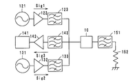
- FIG. 7 is a block diagram of a circuit created by the inventor in an experiment.
- a connector 10 with a switch includes a connector 10 with a switch, signal generators 121 and 131, power amplifiers 122 and 132, an amplifier 142, bandpass filters 123, 133, 143, and 151, a spectrum analyzer 141, and a dummy load 152.
- the signal generator 121 generates a high frequency signal Sig1 having a frequency F1.
- the power amplifier 122 amplifies the high frequency signal Sig1.
- the bandpass filter 123 has a pass band that allows the high-frequency signal Sig1 to pass through, and has an attenuation region that attenuates a high-frequency signal Sig2 and an intermodulation distortion Sig3, which will be described later, by a predetermined amount or more.
- the signal generator 131 generates a high frequency signal Sig2 having a frequency F2 (> F1).
- the power amplifier 132 amplifies the high frequency signal Sig2.
- the band-pass filter 133 has a pass band that allows the high-frequency signal Sig2 to pass therethrough, and has an attenuation region that attenuates the high-frequency signal Sig1 and intermodulation distortion Sig3 described later by a predetermined amount or more.
- the band-pass filter 143 has a pass band that allows passage of intermodulation distortion Sig3, which will be described later, and has an attenuation band that attenuates the high-frequency signals Sig1 and Sig2 by a predetermined amount or more.
- the amplifier 142 amplifies the output from the band pass filter 143 and outputs it to the spectrum analyzer 141.
- the high-frequency signals Sig 1 and Sig 2 that have passed through the switch-equipped connector 10 pass through the band-pass filter 151 and are consumed by the dummy load 152.
- the band pass filter 151 prevents the intermodulation distortion generated in the dummy load 152 from flowing back to the connector 10 with switch and being input to the amplifier 142.
- intermodulation distortion Sig3 having the frequency FIM is generated in the connector with switch 10.
- the frequency FIM is 2F1-F2 or 2F2-F1.
- the frequency FIM is 3F1-2F2 or 3F2-2F1. Further higher order intermodulation distortion is also generated.
- the intermodulation distortion Sig3 passes through the bandpass filter 143, is amplified by the amplifier 142, and is input to the spectrum analyzer 141.
- the inventor of the present application examined the intensity of the third-order intermodulation distortion Sig3 generated in the connector 10 with the switch by using the spectrum analyzer 141. In addition, as a comparison object, the inventor of the present application also examined the strength of the intermodulation distortion Sig3 generated in the connector with a switch not provided with the magnet 100 by the same method.
- the strength of the intermodulation distortion Sig3 was ⁇ 103 dB to ⁇ 105 dB in the connector with a switch not provided with the magnet 100.
- the intensity of the intermodulation distortion Sig3 was ⁇ 118 dB (below the measurement limit). Therefore, it can be seen that the provision of the magnet 100 suppresses intermodulation distortion.
- the present invention is useful for a connector with a switch, and is particularly excellent in that the occurrence of intermodulation distortion can be suppressed.
Landscapes
- Details Of Connecting Devices For Male And Female Coupling (AREA)
- Coupling Device And Connection With Printed Circuit (AREA)
Abstract
L'invention concerne un connecteur pourvu d'un interrupteur, qui permet d'inhiber la distorsion d'intermodulation. Une borne fixe (22) est montée sur la surface d'un boîtier inférieur (18), du côté positif de celui-ci par rapport à l'axe z. Une borne amovible (20) est formée par l'application d'un revêtement de Ni et d'un revêtement d'Au sur de l'acier inoxydable à base d'austénite, et est pressé détachable contre la borne fixe (22). Un aimant (100) est monté sur la surface du boîtier inférieur (18), du côté négatif par rapport à l'axe z, et placé dans une position éloignée par rapport à la borne fixe (22) et à la borne amovible (20).
Priority Applications (2)
| Application Number | Priority Date | Filing Date | Title |
|---|---|---|---|
| JP2013517894A JP5679053B2 (ja) | 2011-06-02 | 2012-02-17 | スイッチ付きコネクタ |
| US14/073,609 US9385490B2 (en) | 2011-06-02 | 2013-11-06 | Switch-equipped connector |
Applications Claiming Priority (2)
| Application Number | Priority Date | Filing Date | Title |
|---|---|---|---|
| JP2011124021 | 2011-06-02 | ||
| JP2011-124021 | 2011-06-02 |
Related Child Applications (1)
| Application Number | Title | Priority Date | Filing Date |
|---|---|---|---|
| US14/073,609 Continuation US9385490B2 (en) | 2011-06-02 | 2013-11-06 | Switch-equipped connector |
Publications (1)
| Publication Number | Publication Date |
|---|---|
| WO2012164980A1 true WO2012164980A1 (fr) | 2012-12-06 |
Family
ID=47258848
Family Applications (1)
| Application Number | Title | Priority Date | Filing Date |
|---|---|---|---|
| PCT/JP2012/053848 Ceased WO2012164980A1 (fr) | 2011-06-02 | 2012-02-17 | Connecteur pourvu d'un interrupteur |
Country Status (3)
| Country | Link |
|---|---|
| US (1) | US9385490B2 (fr) |
| JP (1) | JP5679053B2 (fr) |
| WO (1) | WO2012164980A1 (fr) |
Families Citing this family (10)
| Publication number | Priority date | Publication date | Assignee | Title |
|---|---|---|---|---|
| CN103915703B (zh) * | 2014-03-05 | 2019-09-20 | 连展科技电子(昆山)有限公司 | 微型射频连接器 |
| JP6296037B2 (ja) * | 2015-10-22 | 2018-03-20 | Smk株式会社 | コンタクトの接触構造 |
| US9705242B1 (en) | 2015-12-18 | 2017-07-11 | Microsoft Technology Licensing, Llc | Electrical connector |
| JP2018055994A (ja) * | 2016-09-29 | 2018-04-05 | Smk株式会社 | ソケットのアーク放電防止構造 |
| US20180097485A1 (en) * | 2016-10-03 | 2018-04-05 | United States Of America As Represented By Secretary Of The Navy | HPA Bypass Switch |
| US10355402B2 (en) * | 2017-09-29 | 2019-07-16 | Apple Inc. | Axisymmetric magnetic articulating connector |
| US11811174B2 (en) | 2020-09-25 | 2023-11-07 | Apple Inc. | Low-profile axisymmetric power connectors |
| CN112234547B (zh) * | 2020-10-09 | 2021-11-23 | 湖南鑫锋电子科技有限公司 | 一种磁吸数据线接头 |
| CN112769013A (zh) * | 2021-01-03 | 2021-05-07 | 昆山嘉华电子有限公司 | 同轴连接器 |
| US12261385B2 (en) | 2022-03-07 | 2025-03-25 | Apple Inc. | Power connector with asymmetric insertion-to-extraction force ratio |
Citations (2)
| Publication number | Priority date | Publication date | Assignee | Title |
|---|---|---|---|---|
| JP2004342501A (ja) * | 2003-05-16 | 2004-12-02 | Murata Mfg Co Ltd | 同軸コネクタ及び通信装置 |
| JP2008078134A (ja) * | 2006-09-20 | 2008-04-03 | United Technol Corp <Utc> | 電気的相互接続部および電気的な接続を提供するシステム |
Family Cites Families (15)
| Publication number | Priority date | Publication date | Assignee | Title |
|---|---|---|---|---|
| JP4100727B2 (ja) | 1996-05-15 | 2008-06-11 | 株式会社村田製作所 | 高周波コネクタ |
| JP3064906B2 (ja) * | 1996-06-12 | 2000-07-12 | 株式会社村田製作所 | 同軸コネクタ |
| JP3642112B2 (ja) | 1996-06-21 | 2005-04-27 | 株式会社村田製作所 | 高周波における金属透磁率の測定方法および測定装置 |
| JP2004247625A (ja) | 2003-02-17 | 2004-09-02 | Sony Corp | 露光方法、半導体装置の製造方法、マスクパターンおよび位置ずれ測定方法 |
| JP4288967B2 (ja) | 2003-03-14 | 2009-07-01 | 株式会社村田製作所 | スイッチ付き同軸コネクタ及び通信装置 |
| JP4100204B2 (ja) | 2003-03-14 | 2008-06-11 | 株式会社村田製作所 | スイッチ付き同軸コネクタ及び通信装置 |
| DE102005025403A1 (de) * | 2004-10-29 | 2006-05-18 | Rohde & Schwarz Gmbh & Co Kg | Elektrische Schaltvorrichtung mit magnetischen Verstellelementen |
| JP2007305516A (ja) * | 2006-05-15 | 2007-11-22 | Fujitsu Ltd | 同軸コネクタ、コネクタ組立体、プリント基板、及び電子装置 |
| US7264479B1 (en) | 2006-06-02 | 2007-09-04 | Lee Vincent J | Coaxial cable magnetic connector |
| ATE557453T1 (de) * | 2008-06-25 | 2012-05-15 | Murata Manufacturing Co | Koaxialstecker |
| CN201252276Y (zh) * | 2008-07-02 | 2009-06-03 | 富士康(昆山)电脑接插件有限公司 | 电连接器 |
| JP5119112B2 (ja) * | 2008-07-30 | 2013-01-16 | 富士通コンポーネント株式会社 | 雄コネクタ、雌コネクタ及びコネクタ |
| EP2256874B1 (fr) * | 2009-05-29 | 2012-01-04 | Tyco Electronics Nederland B.V. | Connecteur à commutation miniature |
| JP5330197B2 (ja) * | 2009-11-13 | 2013-10-30 | 富士通コンポーネント株式会社 | コネクタ装置、及び雌コネクタ |
| JP5472272B2 (ja) * | 2011-12-05 | 2014-04-16 | 株式会社村田製作所 | 同軸コネクタプラグ及びその製造方法 |
-
2012
- 2012-02-17 WO PCT/JP2012/053848 patent/WO2012164980A1/fr not_active Ceased
- 2012-02-17 JP JP2013517894A patent/JP5679053B2/ja active Active
-
2013
- 2013-11-06 US US14/073,609 patent/US9385490B2/en active Active
Patent Citations (2)
| Publication number | Priority date | Publication date | Assignee | Title |
|---|---|---|---|---|
| JP2004342501A (ja) * | 2003-05-16 | 2004-12-02 | Murata Mfg Co Ltd | 同軸コネクタ及び通信装置 |
| JP2008078134A (ja) * | 2006-09-20 | 2008-04-03 | United Technol Corp <Utc> | 電気的相互接続部および電気的な接続を提供するシステム |
Also Published As
| Publication number | Publication date |
|---|---|
| US20140065845A1 (en) | 2014-03-06 |
| US9385490B2 (en) | 2016-07-05 |
| JP5679053B2 (ja) | 2015-03-04 |
| JPWO2012164980A1 (ja) | 2015-02-23 |
Similar Documents
| Publication | Publication Date | Title |
|---|---|---|
| JP5679053B2 (ja) | スイッチ付きコネクタ | |
| EP3120160B1 (fr) | Dispositif de détection de champ magnétique et transducteur de courant associé | |
| EP2175531B1 (fr) | Connecteur coaxial | |
| WO2014013834A1 (fr) | Connecteur coaxial | |
| TW201310489A (zh) | 電磁繼電器及其製造方法 | |
| JP5835491B2 (ja) | 同軸コネクタ | |
| TW201448382A (zh) | 同軸連接器 | |
| CN109565099A (zh) | 下谐振环行器及其制造方法 | |
| CN215418638U (zh) | 同轴连接器组的接地连接构造及同轴连接器组 | |
| CN118891528A (zh) | 用于防止信号损失的测试插座 | |
| US20140062633A1 (en) | Coil component | |
| JP2015130266A (ja) | 同軸コネクタ装置 | |
| US9532492B2 (en) | Electromagnetic protection device able to protect a microwave connection between a connector and a microwave element | |
| JP2012104595A (ja) | ノイズ抑制装置 | |
| JP2007288701A (ja) | 非可逆回路素子 | |
| JP2022170628A (ja) | 電流検出装置 | |
| JP2003027278A (ja) | 金属間接触表面構造およびコネクタ | |
| JP2017062220A (ja) | 被測定電流線の固定具及び固定方法並びに電流センサ | |
| JP6198018B2 (ja) | 磁気接合式コネクタ | |
| JP3893934B2 (ja) | 分配ブースタ | |
| JP2022189133A (ja) | コネクタセット、及び同軸コネクタ | |
| CN117767041A (zh) | 一种线缆组件及线缆连接器 | |
| WO2025197946A1 (fr) | Dispositif de mesure de perméabilité et procédé de mesure de perméabilité | |
| JP2015125963A (ja) | 同軸コネクタ装置 | |
| JP2013105656A (ja) | 同軸コネクタ |
Legal Events
| Date | Code | Title | Description |
|---|---|---|---|
| 121 | Ep: the epo has been informed by wipo that ep was designated in this application |
Ref document number: 12793619 Country of ref document: EP Kind code of ref document: A1 |
|
| ENP | Entry into the national phase |
Ref document number: 2013517894 Country of ref document: JP Kind code of ref document: A |
|
| NENP | Non-entry into the national phase |
Ref country code: DE |
|
| 122 | Ep: pct application non-entry in european phase |
Ref document number: 12793619 Country of ref document: EP Kind code of ref document: A1 |