WO2012165016A1 - Liquide de polissage mécano-chimique, et procédé de polissage de substrat semi-conducteur - Google Patents
Liquide de polissage mécano-chimique, et procédé de polissage de substrat semi-conducteur Download PDFInfo
- Publication number
- WO2012165016A1 WO2012165016A1 PCT/JP2012/058187 JP2012058187W WO2012165016A1 WO 2012165016 A1 WO2012165016 A1 WO 2012165016A1 JP 2012058187 W JP2012058187 W JP 2012058187W WO 2012165016 A1 WO2012165016 A1 WO 2012165016A1
- Authority
- WO
- WIPO (PCT)
- Prior art keywords
- polishing
- semiconductor substrate
- polishing liquid
- main surface
- cmp
- Prior art date
- Legal status (The legal status is an assumption and is not a legal conclusion. Google has not performed a legal analysis and makes no representation as to the accuracy of the status listed.)
- Ceased
Links
Images


Classifications
-
- H—ELECTRICITY
- H10—SEMICONDUCTOR DEVICES; ELECTRIC SOLID-STATE DEVICES NOT OTHERWISE PROVIDED FOR
- H10P—GENERIC PROCESSES OR APPARATUS FOR THE MANUFACTURE OR TREATMENT OF DEVICES COVERED BY CLASS H10
- H10P52/00—Grinding, lapping or polishing of wafers, substrates or parts of devices
- H10P52/40—Chemomechanical polishing [CMP]
- H10P52/403—Chemomechanical polishing [CMP] of conductive or resistive materials
-
- H—ELECTRICITY
- H10—SEMICONDUCTOR DEVICES; ELECTRIC SOLID-STATE DEVICES NOT OTHERWISE PROVIDED FOR
- H10P—GENERIC PROCESSES OR APPARATUS FOR THE MANUFACTURE OR TREATMENT OF DEVICES COVERED BY CLASS H10
- H10P52/00—Grinding, lapping or polishing of wafers, substrates or parts of devices
-
- C—CHEMISTRY; METALLURGY
- C09—DYES; PAINTS; POLISHES; NATURAL RESINS; ADHESIVES; COMPOSITIONS NOT OTHERWISE PROVIDED FOR; APPLICATIONS OF MATERIALS NOT OTHERWISE PROVIDED FOR
- C09G—POLISHING COMPOSITIONS; SKI WAXES
- C09G1/00—Polishing compositions
- C09G1/02—Polishing compositions containing abrasives or grinding agents
-
- C—CHEMISTRY; METALLURGY
- C09—DYES; PAINTS; POLISHES; NATURAL RESINS; ADHESIVES; COMPOSITIONS NOT OTHERWISE PROVIDED FOR; APPLICATIONS OF MATERIALS NOT OTHERWISE PROVIDED FOR
- C09K—MATERIALS FOR MISCELLANEOUS APPLICATIONS, NOT PROVIDED FOR ELSEWHERE
- C09K3/00—Materials not provided for elsewhere
- C09K3/14—Anti-slip materials; Abrasives
-
- C—CHEMISTRY; METALLURGY
- C09—DYES; PAINTS; POLISHES; NATURAL RESINS; ADHESIVES; COMPOSITIONS NOT OTHERWISE PROVIDED FOR; APPLICATIONS OF MATERIALS NOT OTHERWISE PROVIDED FOR
- C09K—MATERIALS FOR MISCELLANEOUS APPLICATIONS, NOT PROVIDED FOR ELSEWHERE
- C09K3/00—Materials not provided for elsewhere
- C09K3/14—Anti-slip materials; Abrasives
- C09K3/1409—Abrasive particles per se
-
- C—CHEMISTRY; METALLURGY
- C09—DYES; PAINTS; POLISHES; NATURAL RESINS; ADHESIVES; COMPOSITIONS NOT OTHERWISE PROVIDED FOR; APPLICATIONS OF MATERIALS NOT OTHERWISE PROVIDED FOR
- C09K—MATERIALS FOR MISCELLANEOUS APPLICATIONS, NOT PROVIDED FOR ELSEWHERE
- C09K3/00—Materials not provided for elsewhere
- C09K3/14—Anti-slip materials; Abrasives
- C09K3/1454—Abrasive powders, suspensions and pastes for polishing
- C09K3/1463—Aqueous liquid suspensions
-
- H—ELECTRICITY
- H10—SEMICONDUCTOR DEVICES; ELECTRIC SOLID-STATE DEVICES NOT OTHERWISE PROVIDED FOR
- H10W—GENERIC PACKAGES, INTERCONNECTIONS, CONNECTORS OR OTHER CONSTRUCTIONAL DETAILS OF DEVICES COVERED BY CLASS H10
- H10W20/00—Interconnections in chips, wafers or substrates
- H10W20/01—Manufacture or treatment
- H10W20/021—Manufacture or treatment of interconnections within wafers or substrates
- H10W20/023—Manufacture or treatment of interconnections within wafers or substrates the interconnections being through-semiconductor vias
-
- H—ELECTRICITY
- H10—SEMICONDUCTOR DEVICES; ELECTRIC SOLID-STATE DEVICES NOT OTHERWISE PROVIDED FOR
- H10W—GENERIC PACKAGES, INTERCONNECTIONS, CONNECTORS OR OTHER CONSTRUCTIONAL DETAILS OF DEVICES COVERED BY CLASS H10
- H10W20/00—Interconnections in chips, wafers or substrates
- H10W20/01—Manufacture or treatment
- H10W20/021—Manufacture or treatment of interconnections within wafers or substrates
- H10W20/023—Manufacture or treatment of interconnections within wafers or substrates the interconnections being through-semiconductor vias
- H10W20/0245—Manufacture or treatment of interconnections within wafers or substrates the interconnections being through-semiconductor vias comprising use of blind vias during the manufacture
Definitions
- the present invention relates to a CMP polishing liquid and a method for polishing a semiconductor substrate, and more particularly to a CMP polishing liquid suitable for processing a main surface of a semiconductor substrate and a method for polishing a semiconductor substrate.
- Non-Patent Document 1 Over the years, high performance of semiconductor devices has been achieved by miniaturization and high integration based on scaling rules (for example, see Non-Patent Document 1 below). However, in recent years, such an approach has reached its limit, and the direction is changing toward higher performance in the entire system including design and implementation.
- LSI Large-Scale Integrated Circuit
- the original mounting technique is one of them (for example, see Non-Patent Document 2 below).
- TSV Through-silicon Via
- a semiconductor substrate having a TSV structure is manufactured as follows. First, an insulating layer (for example, a silicon oxide film (silicon dioxide film)) for insulating TSV is formed on the surface of a semiconductor substrate (for example, a silicon substrate) in which a hollow portion opened only on the surface (one main surface) is formed. ) Along the shape of the hollow portion. Next, a conductive member (for example, a conductor layer such as a copper layer) that is a TSV material is disposed in the hollow portion.
- a conductive member for example, a conductor layer such as a copper layer
- the polishing liquid for producing a semiconductor substrate contains, for example, any one of colloidal silica and silica gel in which the primary particle size is in the range of 4 to 200 nm (preferably 4 to 100 nm), and a water-soluble amine.
- a polishing liquid is mentioned (for example, refer to the above-mentioned patent document 1).
- a polishing liquid for manufacturing a semiconductor substrate is mainly made of a constituent material of a semiconductor substrate such as silicon
- the polishing rate of the insulating layer when the polishing liquid is used is very low. Therefore, even when the insulating layer covering the conductive member is polished using such a polishing liquid for manufacturing a semiconductor substrate, the insulating layer remains and the conductive member is hardly exposed.
- a step of polishing the insulating layer using a polishing liquid for polishing the insulating layer and a step of removing the insulating layer by a method such as wet etching or dry etching are separately required. The process for obtaining the through electrode becomes complicated.
- the present invention is intended to solve the above problems, and a CMP polishing liquid capable of polishing a semiconductor substrate, an insulating layer, and a conductive member at an excellent polishing rate, and polishing of a semiconductor substrate using the CMP polishing liquid. It aims to provide a method.
- the depth of the conductive member from the surface to be polished of the substrate may be different from each other depending on the position and arrangement of the conductive members in the semiconductor substrate.
- polishing is continued until the conductive member formed at the deepest position from the surface to be polished is exposed, and the already exposed conductive members are insulated. It must be polished with layers and semiconductor substrates. For this reason, the present inventors have come to the idea that it is necessary to polish the semiconductor substrate, the insulating layer and the conductive member at an excellent polishing rate for the CMP polishing liquid.
- the CMP polishing liquid according to the present invention comprises abrasive grains containing ceria particles and silica particles, a compound having a first acid dissociation constant of 7 or less (excluding azoles), a basic compound, and a persulfate salt.
- the CMP polishing liquid has a pH of 9.0 to 12.0.
- the acid dissociation constant (pKa) is the negative common logarithm (logarithm of the reciprocal) of the equilibrium constant Ka in the dissociation reaction in which hydrogen ions are released from the acid.
- first acid dissociation constant (pKa1) The acid dissociation constant of the eye.
- the compound having a first acid dissociation constant of 7 or less may be a compound having a single pKa.
- the single pKa is referred to as “pKa1”.
- As the value of pKa1 for example, Chemical Handbook, Basic Edition II (5th revised edition, Maruzen Co., Ltd.) can be referred to.
- the semiconductor substrate, the insulating layer, and the conductive member can be polished at an excellent polishing rate.
- a through electrode structure can be easily formed without providing a process for exposing the conductive member and complicating the process.
- a through electrode structure having a plurality of through electrodes can be easily formed.
- a plurality of semiconductor substrates having a first conductive member formed at a shallow position from a surface to be polished and a second conductive member formed at a position deep from the surface to be polished are used.
- a through electrode structure having the through electrodes can be easily formed.
- the insulating layer covering the first conductive member and the surface layer portion of the semiconductor substrate are simultaneously polished, so that the first conductive member is polished on the surface to be polished. It exposes and the 1st penetration electrode is obtained.
- the second conductive member is polished by simultaneously polishing the surface layer portion of the semiconductor substrate, the insulating layer and the first conductive member exposed on the surface to be polished using the CMP polishing liquid according to the present invention. A second through electrode is obtained by exposing to the surface. Thereby, the penetration electrode structure which has a some penetration electrode can be formed easily.
- the compound having a first acid dissociation constant of 7 or less preferably contains an amino acid.
- the amino acid is preferably an ⁇ -amino acid.
- the semiconductor substrate, the insulating layer, and the conductive member can be polished at a further excellent polishing rate.
- the compound having a first acid dissociation constant of 7 or less may contain an organic acid having a carboxyl group. Even in this case, the semiconductor substrate, the insulating layer, and the conductive member can be polished at a further excellent polishing rate.
- the basic compound preferably includes at least one selected from nitrogen-containing basic compounds and inorganic basic compounds, and includes at least one selected from potassium hydroxide, sodium hydroxide, tetramethylammonium hydroxide, and ammonium hydroxide. It is more preferable. In these cases, the semiconductor substrate, the insulating layer, and the conductive member can be polished at a further excellent polishing rate.
- the content of the basic compound is preferably 0.10% by mass or more.
- the semiconductor substrate, the insulating layer, and the conductive member can be polished at a further excellent polishing rate.
- the persulfate preferably contains at least one selected from potassium persulfate and ammonium persulfate.
- the semiconductor substrate, the insulating layer, and the conductive member can be polished at a further excellent polishing rate.
- a CMP polishing liquid according to the present invention comprises a substrate body of a semiconductor substrate comprising a substrate body in which a hollow portion opened only on one main surface is formed, and a conductive member to be a through electrode disposed in the hollow portion. May be used to form a through electrode structure by polishing the electrode from the other main surface side and exposing the conductive member to the other main surface side.
- a CMP polishing liquid according to the present invention is a substrate of a semiconductor substrate comprising a substrate body in which a through hole penetrating from one main surface to the other main surface is formed, and a through electrode disposed in the through hole. It may be used for polishing the main body from the one main surface side or the other main surface side.
- a method for polishing a semiconductor substrate according to the present invention includes: a substrate body having a hollow portion that is open only on one main surface; and a conductive member that is to be a through electrode and is disposed in the hollow portion.
- the substrate main body may be polished from the other main surface side using the CMP polishing liquid, and a conductive member may be exposed to the other main surface side to form a through electrode structure. According to such a polishing method, a through electrode structure having a plurality of through electrodes can be easily formed.
- a semiconductor substrate polishing method includes a substrate body in which a through-hole penetrating from one main surface to the other main surface is formed, and a through-electrode disposed in the through-hole.
- a polishing step of polishing the substrate main body from the one main surface side or the other main surface side using the CMP polishing liquid may be provided.
- the semiconductor substrate, the insulating layer, and the through electrode are exposed on the surface to be polished by using a CMP polishing liquid that can polish the semiconductor substrate, the insulating layer, and the conductive member at an excellent polishing rate.
- the length of the through electrode can be adjusted while maintaining a good state.
- the second through electrode is adjusted while adjusting the length of the first through electrode. Can also be formed.
- the method for polishing a semiconductor substrate according to the present invention may further include a step of grinding the substrate body from the main surface side polished in the polishing step before the polishing step.
- polishing cloth polishing pad having a Shore D hardness of 30 to 90 in the polishing step.
- polishing cloth polishing pad having a Shore D hardness of 30 to 90 in the polishing step.
- a CMP polishing liquid capable of polishing a semiconductor substrate, an insulating layer and a conductive member at an excellent polishing rate, and a semiconductor substrate polishing method using the CMP polishing liquid.
- a through electrode structure can be easily formed without providing a process for exposing the conductive member and complicating the process.
- a through electrode structure having a through electrode can be easily formed.
- the CMP polishing liquid according to this embodiment includes abrasive grains (polishing particles), a compound having a first acid dissociation constant (pKa1) of 7 or less (excluding azoles), a basic compound, an oxidizing agent, Containing.
- the CMP polishing liquid according to the present embodiment includes at least ceria particles (cerium oxide particles) and silica particles (silicon dioxide particles) as abrasive grains.
- a surface to be polished from which a semiconductor substrate (for example, a silicon substrate) and an insulating layer (for example, a silicon oxide film) are exposed using such a polishing liquid the semiconductor substrate is mainly polished by silica particles, and ceria particles It is considered that the insulating layer is mainly polished by this, but as a whole, a good polishing rate can be obtained by the synergistic effect of both.
- the silica particles colloidal silica particles are preferable.
- abrasive grains may be used in combination as necessary.
- specific examples of other abrasive grains that can be used in combination include abrasive grains made of an inorganic material such as alumina, titania or zirconia; abrasive grains made of an organic material such as an organic polymer; composite abrasive made of an organic material and an inorganic material A grain etc. can be mentioned.
- the average particle diameter (secondary particle diameter) of the ceria particles is preferably 500 nm or less, and preferably 400 nm or less in that the dispersion stability in the polishing liquid is good and the number of polishing scratches (scratches) generated by CMP is small. More preferred.
- the average particle size of the ceria particles is preferably 10 nm or more, more preferably 30 nm or more, and even more preferably 50 nm or more in that a practical polishing rate can be easily obtained.
- the content of the ceria particles is preferably 0.01% by mass or more, and preferably 0.05% by mass or more based on the total mass of the polishing liquid from the viewpoint that the polishing rate of the insulating layer (eg, silicon oxide film) can be sufficiently improved. More preferably, 0.10% by mass or more is further preferable, and 0.20% by mass or more is particularly preferable.
- the content of the ceria particles is preferably 2.00% by mass or less, more preferably 1.00% by mass or less, based on the total mass of the polishing liquid, in that the aggregation of particles in the polishing liquid can be easily suppressed. 0.80% by mass or less is more preferable.
- the average particle size (secondary particle size) of the silica particles is preferably 200 nm or less, and preferably 100 nm or less in that the dispersion stability in the polishing liquid is good and the number of polishing scratches (scratches) generated by CMP is small. More preferred.
- the silica particles are preferably colloidal silica having an average particle size of 200 nm or less, and more preferably colloidal silica having an average particle size of 100 nm or less.
- the average particle size of the silica particles is preferably 5 nm or more, more preferably 7 nm or more, and even more preferably 9 nm or more in that it is easy to obtain a practical polishing rate.
- the content of the silica particles is preferably 0.01% by mass or more, more preferably 0.05% by mass or more based on the total mass of the polishing liquid in that the polishing rate of the semiconductor substrate (eg, silicon substrate) can be sufficiently improved.
- the polishing rate of the semiconductor substrate eg, silicon substrate
- 0.10 mass% or more is more preferable.
- the content of the silica particles is preferably 5.00% by mass or less on the basis of the total mass of the polishing liquid in that it is easy to obtain an effect of improving the polishing rate commensurate with the content while suppressing the occurrence of defects such as polishing scratches. 0.000 mass% or less is more preferable, and 0.50 mass% or less is still more preferable.
- the average particle size of the ceria particles can be measured with a laser diffraction particle size distribution analyzer (for example, LA-920 manufactured by Horiba, Ltd.). Specifically, it can be measured as follows using LA-920 (light source: He—Ne laser and W laser) manufactured by Horiba. First, a ceria particle dispersion having a measurement transmittance (H) of 65 to 75% for a He—Ne laser is obtained as a measurement sample. Then, this measurement sample was put into LA-920 and measured as a relative refractive index of 1.60 (theoretical refractive index of cerium oxide 2.128 / refractive index of water 1.33). As the size, the average particle size (secondary particle size) of the ceria particles can be obtained.
- LA-920 light source: He—Ne laser and W laser
- the average particle diameter of the silica particles can be measured with a dynamic light scattering particle size distribution analyzer (for example, trade name COULTER N4 SD manufactured by COULTER Electronics). Specifically, the dispersion of silica particles is weighed, and if necessary, dilute the dispersion with water so that it falls within the range of scattered light intensity required by the dynamic light scattering particle size distribution analyzer. Prepare. Next, this measurement sample is put into a dynamic light scattering system particle size distribution meter and measured in the scattered light reference mode, whereby an average particle diameter (secondary particle diameter) of silica particles is obtained as D50.
- a dynamic light scattering particle size distribution analyzer for example, trade name COULTER N4 SD manufactured by COULTER Electronics.
- the CMP polishing liquid according to the present embodiment contains a compound having a first acid dissociation constant of 7 or less (excluding azoles).
- An azole not corresponding to the compound means a compound having a hetero 5-membered ring containing one or more nitrogen atoms in the ring, such as 1H-1,2,4-triazole, 3-amino-1H-1, And triazoles such as 2,4-triazole and derivatives thereof.
- the CMP polishing liquid is prevented from being excessively high in pH, for example, at a desired pH (eg, 9.0 to 12.0). It is possible to increase the content of a basic compound that functions as a solubilizer for the constituent material (silicon or the like) of the semiconductor substrate. As a result, it is possible to significantly increase the polishing rate of the constituent material (silicon or the like) of the semiconductor substrate as compared with a polishing liquid not containing a compound having a first acid dissociation constant of 7 or less.
- the first acid dissociation constant of the compound is preferably 5 or less, and more preferably 4 or less.
- the compound having a first acid dissociation constant of 7 or less is selected from amino acids and organic acids having a carboxyl group (except for amino acids) in that the content of the basic compound can be further increased. At least one is preferred.
- the “amino acid” is defined as an organic compound having functional groups of both an amino group and a carboxyl group. Of the amino acids, ⁇ -amino acids are more preferred.
- amino acid having a first acid dissociation constant of 7 or less examples include glycine, histidine (eg, L-histidine), aspartic acid, glutamic acid, leucine, serine, proline, valine and the like, and at least one selected from glycine and histidine Is preferred.
- Examples of the organic acid having a carboxyl group and a first acid dissociation constant of 7 or less include malic acid, picolinic acid, maleic acid, malonic acid, citric acid, gluconic acid, glycolic acid, succinic acid, lactic acid, adipic acid, Examples include glutaric acid, benzoic acid, phthalic acid, fumaric acid, oxalic acid, tartaric acid, nicotinic acid, mandelic acid, acetic acid, quinaldic acid, butyric acid, valeric acid, salicylic acid, glyceric acid, and pimelic acid. Acid and maleic acid are preferable, and malic acid is more preferable.
- the compound whose 1st acid dissociation constant is 7 or less can be used individually by 1 type or in combination of 2 or more types.
- a combination of compounds having a first acid dissociation constant of 7 or less for example, a combination of glycine and malic acid can be used.
- the content of the compound having a first acid dissociation constant of 7 or less is preferably 0.10% by mass or more, based on the total mass of the polishing liquid, and is preferably 0.20% in that the effect of improving the polishing rate can be sufficiently obtained. % Or more is more preferable, and 0.30 mass% or more is still more preferable.
- the content of the compound having a first acid dissociation constant of 7 or less is such that a problem such as abrasive grains agglomerating occurs in the storage liquid for polishing liquid that is diluted with a liquid medium such as water at the time of use.
- it is preferably 3.00% by mass or less, more preferably 1.00% by mass or less, and still more preferably 0.70% by mass or less, based on the total mass of the polishing liquid.
- the CMP polishing liquid according to this embodiment contains a basic compound that functions as a solubilizer for the constituent material (silicon or the like) of the semiconductor substrate.
- the basic compound preferably contains at least one selected from nitrogen-containing basic compounds and inorganic basic compounds.
- the nitrogen-containing basic compound is not particularly limited, but at least one selected from tetramethylammonium hydroxide and ammonium hydroxide is preferable.
- Examples of the inorganic basic compound include potassium hydroxide and sodium hydroxide, and potassium hydroxide is preferable.
- ammonium hydroxide is preferable from the viewpoint of further improving the polishing rate of the conductive member. Since ammonium hydroxide forms an ammine complex with a metal component (for example, copper) of the conductive member, and dissolution of the metal component is promoted, it is presumed that the polishing rate of the conductive member is further improved.
- a metal component for example, copper
- a basic compound can be used individually by 1 type or in combination of 2 or more types.
- a combination of the basic compounds a combination of potassium hydroxide and ammonium hydroxide is preferable because the semiconductor substrate, the insulating layer, and the conductive member can be polished at an excellent polishing rate.
- the content of the basic compound is preferably 0.10% by mass or more, more preferably 0.20% by mass or more, based on the total mass of the polishing liquid, in that it is easy to obtain a practical polishing rate for a semiconductor substrate. 30 mass% or more is still more preferable.
- the content of the basic compound is 5.00 on the basis of the total mass of the polishing liquid in that it is possible to easily prevent problems such as depolymerization of the silica particles as abrasive grains and aggregation due to an increase in ionic strength. % By mass or less is preferable, 3.00% by mass or less is more preferable, and 1.00% by mass or less is more preferable.
- When using a some compound as a basic compound it is preferable that the sum total of content of each compound satisfy
- the content of a basic compound (such as ammonium hydroxide) complexed with a metal component (for example, copper) is preferably 0.50% by mass or less from the viewpoint of suppressing excessive dissolution of the conductive member.
- a basic compound such as ammonium hydroxide
- a metal component for example, copper
- the CMP polishing liquid according to the present embodiment contains persulfate as an oxidizing agent from the viewpoint of improving the polishing rate of the conductive member while maintaining a high polishing rate of the semiconductor substrate and the insulating layer.
- persulfate examples include potassium persulfate, ammonium persulfate, and oxone (registered trademark), and at least one selected from potassium persulfate and ammonium persulfate is preferable.
- the oxidizing agent is other than persulfate (for example, hydrogen peroxide solution), the principle is not clear at present, but problems such as yellowing of the ceria particles and aggregation and precipitation occur.
- the content of the oxidant is preferably 0.05% by mass or more, more preferably 0.07% by mass or more, more preferably 0.10, based on the total mass of the polishing liquid from the viewpoint of sufficiently improving the polishing rate of the conductive member. More preferably, it is more preferably at least 0.20% by mass, particularly preferably at least 0.25% by mass, even more preferably at least 0.30% by mass, and even more preferably at least 0.50% by mass.
- the content of the oxidizing agent is preferably 5.00% by mass or less, based on the total mass of the polishing liquid, in that it is possible to easily suppress the occurrence of defects such as agglomeration of abrasive grains and corrosion of conductive members, and 3.00% by mass. The mass% or less is more preferable, and the 1.00 mass% or less is more preferable.
- the CMP polishing liquid according to the present embodiment includes components generally added to the polishing liquid such as water, solvents other than water, water-soluble polymers and anticorrosives, and the like. It can further contain in the range which does not impair an effect.
- the pH of the CMP polishing liquid according to this embodiment is 9.0 or more, preferably 9.5 or more, and preferably 10.0 or more from the viewpoint of sufficiently improving the polishing rate of the constituent material (silicon or the like) of the semiconductor substrate. Is more preferable.
- the pH of the CMP polishing liquid sufficiently improves the polishing speed of the constituent material (silicon or the like) of the semiconductor substrate, and the abrasive grains undergo depolymerization, thereby reducing the liquid stability of the CMP polishing liquid (for example, Patent Document 2 above). 12.0 or less, preferably 11.5 or less, and more preferably 11.0 or less.
- the pH of the CMP polishing liquid can be adjusted by, for example, the content of a compound having a pKa1 of 7 or less and a basic compound in the CMP polishing liquid.
- the pH of the CMP polishing liquid can be measured with a pH meter (for example, Model pH81, manufactured by Yokogawa Electric Corporation).
- a pH meter for example, Model pH81, manufactured by Yokogawa Electric Corporation.
- two-point calibration is performed using a neutral phosphate pH buffer solution (pH 6.86 (25 ° C.)) and a borate pH standard solution (pH 9.18 (25 ° C.)), and then the electrode Can be used as the pH of the CMP polishing liquid (25 ° C.) after 2 minutes or more have elapsed and stabilized.
- the CMP polishing liquid according to the present embodiment can be stored as a polishing liquid storage liquid in which the content of the components is increased in advance.
- the CMP polishing liquid of the polishing liquid storage liquid may be diluted with water or the like to the original content of the components.
- the CMP polishing liquid according to the present embodiment can be stored as a liquid separation form in which the components are divided into several liquids, and these can be mixed and used at the time of use.
- the CMP polishing liquid according to this embodiment forms a through electrode structure by exposing a conductive member to be a through electrode to the surface to be polished by simultaneous polishing of the substrate body and the insulating layer exposed on the surface to be polished of the semiconductor substrate. In addition, by polishing the polished surface of the semiconductor substrate where the substrate body, the insulating layer, and the first through electrode are exposed, the conductive member to be the through electrode is exposed on the polished surface, and the second through electrode is formed.
- the CMP polishing liquid according to the present embodiment is particularly suitable for an application in which the main surface of a semiconductor substrate having a conductive member to be a through electrode is ground (grinded) in the grinding step, and then the main surface is polished. Yes.
- the first aspect of the semiconductor substrate polishing method is as follows: (1) Between a substrate main body in which a hollow portion opened only on one main surface is formed, a conductive member to be a through electrode disposed in the hollow portion, and the other main surface and hollow portion of the substrate main body A preparation step of preparing a semiconductor substrate comprising at least an insulating layer; and (2) After the preparation step, a grinding step (thinning step) for thinning the substrate body by grinding the substrate body from the other main surface side so that the conductive member is not exposed; (3) After the grinding step, the substrate body and the insulating layer are polished from the other main surface side using the CMP polishing liquid, and a conductive member is exposed to the other main surface side to form a through electrode structure.
- a polishing step In the first aspect of the polishing method, in the polishing step, the insulating layer covering the conductive member on the other main surface side or the surface layer portion of the substrate body is removed by polishing to expose the conductive member to the other main surface side. A through electrode is formed.
- a substrate body 1 such as a silicon substrate having a front surface (one main surface, first main surface) 1a and a back surface (the other main surface, second main surface) 1b facing each other.
- the element 2 is formed on the surface 1a (see FIG. 1A).
- a plurality of hollow portions 3a and 3b for arranging TSVs (through electrodes) are formed on the surface 1a of the substrate body 1 by a method such as plasma etching (see FIG. 1B).
- the depths of the hollow portions 3a and 3b are different from each other, and the bottom surfaces of the hollow portions 3a and 3b are located deeper from the back surface 1b in the hollow portion 3b than in the hollow portion 3a.
- an insulating layer for example, a silicon oxide film or a silicon nitride film
- an insulating layer 5 for insulating the TSV is formed on the surface 1a so as to follow the shape of the hollow portions 3a and 3b to obtain the semiconductor substrate 100 (FIG. 1 (c)).
- a conductive member (for example, a copper layer) 7 is laminated on the insulating layer 5 by a method such as sputtering or electrolytic plating so as to fill the hollow portions 3a and 3b and cover the entire surface of the insulating layer 5 (FIG. 2A )reference). Subsequently, the conductive member 7 and the insulating layer 5 are polished from the surface 1a side until the element 2 is exposed to obtain the semiconductor substrate 200 (see FIG. 2B).
- the substrate body 1 is ground from the back surface 1b side by a grinder until the insulating layer 5a disposed on the bottom surface of the hollow portion 3a is exposed, thereby thinning the substrate body 1 to obtain the semiconductor substrate 300 (FIG. 3). (See (a)).
- the substrate body 1 is polished from the back surface 1b side using the CMP polishing liquid, and a plurality of TSVs are formed while eliminating grinding flaws generated on the back surface 1b by the grinder in the grinding step.
- the conductive member 7 in the hollow portion 3a is exposed to the back surface 1b of the substrate body 1 to form the TSV 7a, and the conductive member 7 in the hollow portion 3b is used as the back surface 1b of the substrate body 1.
- a second polishing step for forming TSV7b for forming TSV7b.
- the first polishing step and the second polishing step may be performed continuously as a single step or may be performed as separate steps.
- a semiconductor substrate 300 to be polished in the first polishing step is a semiconductor substrate for forming a TSV structure (through electrode structure), and includes a substrate body 1 in which hollow portions 3a and 3b opened only on the surface 1a are formed.
- the end portion on the back surface 1b side of the conductive member 7 is covered with the insulating layers 5a and 5b and the surface layer portion on the back surface 1b side of the substrate body 1, and the end portion on the front surface 1a side of the conductive member 7 is on the surface 1a. Exposed.
- the conductive member 7 becomes TSV when the substrate body 1 is polished from the back surface 1b side and the conductive member 7 is exposed to the back surface 1b.
- the surface layer portion on the back surface 1b side of the substrate body 1 is removed, and the insulating layer 5a is exposed to the back surface 1b.
- the insulating layer 5a exposed on the back surface 1b is removed, the conductive member 7 is exposed on the back surface 1b, and a through hole 13a is formed in the substrate body 1 (see FIG. 3B). ).
- the semiconductor substrate 400 having the TSV 7a penetrating the substrate body 1 in the thickness direction from the front surface 1a to the back surface 1b is obtained.
- the semiconductor substrate 400 to be polished in the second polishing step is a semiconductor substrate for further forming the TSV 7b, and is disposed in the hollow body 3b, the substrate body 1 having the hollow portion 3b opened only on the surface 1a.
- the conductive member 7 to be the TSV and the insulating layer 5b disposed between the substrate body 1 and the conductive member 7 along the inner wall of the hollow portion 3b are provided.
- the surface layer portion on the back surface 1b side of the substrate body 1 is removed, and the insulating layer 5b is exposed to the back surface 1b.
- the insulating layer 5a and the TSV 7a in the through hole 13a exposed to the back surface 1b are also removed together with the surface layer portion on the back surface 1b side of the substrate body 1.
- the insulating layer 5b exposed on the back surface 1b is removed, the conductive member 7 is exposed on the back surface 1b, and a through hole 13b is formed in the substrate body 1 (see FIG. 3C). ).
- a semiconductor substrate 500 having a plurality of TSVs 7a and 7b that penetrate the substrate body 1 in the thickness direction from the front surface 1a to the back surface 1b and electrically connect the front surface 1a and the back surface 1b is obtained.
- the second aspect of the method of polishing a semiconductor substrate according to this embodiment is (1) A preparation step of preparing a semiconductor substrate as in the preparation step of the first aspect of the polishing method; (2) After the preparation step, the through hole penetrating from the one main surface to the other main surface is formed by grinding the substrate body from the other main surface side so that the conductive member is exposed. A grinding step for obtaining a semiconductor substrate comprising a substrate body and a through electrode disposed in the through hole; (3) After the grinding step, a polishing step of polishing the substrate body, the insulating layer, and the through electrode from the one main surface side or the other main surface side using the CMP polishing liquid.
- the conductive member in the grinding step, is exposed to the other main surface side to form a through electrode, and in the polishing step, the semiconductor substrate, the insulating layer, and the through hole exposed on the other main surface.
- the semiconductor substrate 100 is prepared as in the first aspect.
- the substrate body 1 is ground from the back surface 1b side by a grinder until the conductive member 7 in the hollow portion 3a and the hollow portion 3b is exposed, so that the substrate body 1 is thinned and the semiconductor substrate 500 (FIG. 3).
- a semiconductor substrate having TSVs 7a and 7b is obtained.
- the obtained semiconductor substrate is an object to be polished in the polishing step in the second aspect, and is disposed in the substrate body 1 in which the through holes 13a and 13b penetrating from the front surface 1a to the back surface 1b are formed, and in the through holes 13a and 13b. TSVs 7a and 7b.
- the substrate body 1 is polished from the back surface 1b side using the CMP polishing liquid, as in the polishing step of the first aspect.
- produced in the back surface 1b in the grinding process can be eliminated.
- the polishing surface plate and the polishing surface plate are pressed while the back surface 1b of the substrate body 1 is pressed against the polishing cloth while supplying the CMP polishing liquid onto the polishing cloth of the polishing surface plate. It is preferable to polish the substrate body 1 from the back surface 1b side by relatively moving the substrate body 1. When such a polishing method is used, the polishing characteristics of the CMP polishing liquid can be significantly improved.
- polishing apparatus used in the polishing process, it is common to have a polishing platen that can be attached to a polishing cloth and connected to a motor that can change the number of rotations, and a holder that can hold a substrate to be polished.
- a simple polishing apparatus can be used.
- polishing cloth A general nonwoven fabric, a polyurethane foam, a porous fluororesin, etc. can be used.
- the rotation speed of the polishing platen is preferably a low rotation of 200 rpm (200 min ⁇ 1 ) or less so that the substrate does not jump out.
- the pressure for pressing the substrate against the polishing cloth (polishing pressure) is preferably 70 to 350 hPa (7 to 35 kPa).
- polishing it is preferable to continuously supply the polishing liquid to the polishing cloth with a pump or the like. Although there is no restriction
- the polishing process includes a rough polishing process for rough polishing the substrate body 1, which is a rough wafer having a grinding flaw on the back surface 1b, from the back surface 1b side, and a precision polishing for precisely polishing the substrate body 1 from the back surface 1b side after the rough polishing step.
- the second polishing step can be performed as the precise polishing step.
- the substrate body 1 In the precision polishing step, it is preferable to polish the substrate body 1 from the back surface 1b side using a polishing cloth having a predetermined Shore D hardness.
- the lower limit of the Shore D hardness of the polishing cloth is preferably 30 or more, and more preferably 40 or more. When the Shore D hardness is 30 or more, it is possible to sufficiently suppress that the polishing cloth enters the TSV portion excessively during polishing and the TSV is greatly dented from the surface to be polished (so-called dishing is large). it can. As a result, the LSI chips stacked one above the other can be connected more satisfactorily.
- the upper limit of the Shore D hardness of the polishing cloth is preferably 90 or less, and more preferably 80 or less. When the Shore D hardness is 90 or less, defects such as scratches caused by polishing can be suppressed.
- Shore D hardness is often used when measuring the hardness of hard rubber or the like, and is a standard corresponding to JIS K 6253.
- the Shore D hardness is a value measured with a Shore D hardness meter, and for measuring the Shore D hardness, for example, “Asker Rubber Hardness Meter Type D” manufactured by Kobunshi Keiki Co., Ltd. can be used. Since a measurement error of about ⁇ 1 generally occurs in the measured value of Shore D hardness, an average value obtained by performing the same measurement five times is used.
- the upper limit of Shore D hardness is 100 from the definition.
- the method for polishing a semiconductor substrate according to the present invention is not limited to the above-described embodiment, and various modifications are possible.
- the grinding step and the polishing step are performed using the semiconductor substrate 100, but the semiconductor substrate 100a shown in FIG.
- the element 2 and the hollow portions 3a and 3b are formed similarly to the semiconductor substrate 100, and an insulating layer (for example, a silicon oxide film or a silicon nitride film) 15 for insulating the TSV is formed in the hollow portions 3a, It is formed on the surface 1a so as to follow the shape of 3b, and a barrier metal layer (for example, a tantalum layer, a tantalum nitride layer, a titanium layer, a titanium nitride layer) on the insulating layer 15 so as to follow the shape of the insulating layer 15 , Tungsten layer, tungsten nitride layer) 25 is formed.
- a barrier metal layer for example, a tantalum layer, a tantalum nitride layer, a titanium layer, a titanium nitride layer
- the substrate body 1 in the semiconductor substrate 100a is ground and polished from the back surface 1b side, and the surface layer portion on the back surface 1b side of the substrate body 1, the insulating layer 15 and the barrier metal layer 25.
- the semiconductor substrate 500a (see FIG. 4B) with the TSVs 7a and 7b exposed on the back surface 1b side is obtained.
- the barrier metal layer 25 is disposed between the TSVs 7a and 7b and the insulating layer 15, Cu, which is a constituent component of the TSVs 7a and 7b, is prevented from diffusing into the substrate body 1, and the TSV 7a. 7b and the insulating layer 15 can be improved.
- the substrate body 1 is ground from the back surface 1b side by the grinder until just before the insulating layer 5 is exposed in the grinding step, but the substrate is ground by the grinder until just before the conductive member 7 is exposed.
- the substrate body 1 may be thinned by grinding the body 1 from the back surface 1b side.
- the polishing step subsequent to the grinding step the substrate body 1 is polished from the back surface 1b side, the insulating layer 5a is removed, and the conductive member 7 is exposed to the back surface 1b, whereby the TSV 7a can be obtained.
- the substrate body 1 is ground from the back surface 1b side until the conductive member 7 in the hollow portion 3a and the hollow portion 3b is exposed in the grinding step. After the conductive member 7 is exposed, the substrate body 1 may be ground from the back surface 1b side until just before the conductive member 7 in the hollow portion 3b is exposed.
- the depths of the plurality of hollow portions are different from each other, but the depths of the plurality of hollow portions may be the same.
- a TSV structure having a plurality of TSVs is formed, but a TSV structure having a single TSV may be formed.
- the CMP polishing liquids of Examples 1 to 10 and Comparative Examples 1 to 7 were prepared according to the following procedure by adjusting the content of each component to the amounts shown in Tables 1 to 3.
- potassium hydroxide and ammonia hydroxide which are basic compounds, were added using an aqueous solution in consideration of the concentration of the aqueous solution so as to be a predetermined amount in the polishing liquid.
- silica particles (colloidal silica particles) and ceria particles, which are abrasive grains were added using an aqueous dispersion in consideration of the abrasive content of the aqueous dispersion so as to be a predetermined amount in the polishing liquid.
- persulfate as an oxidizing agent was added in consideration of the concentration of the aqueous solution so that a 10% by mass aqueous solution was prepared and a predetermined amount was obtained in the polishing liquid.
- Examples 1 to 10 After dissolving compound A in Table 1 or Table 2 (compound having a first acid dissociation constant of 7 or less) in pure water corresponding to 50% by mass of the entire polishing liquid, a predetermined amount of a basic compound was added. . Next, silica particles (colloidal silica particles having a secondary particle size of about 25 nm) were added so that the abrasive content would be the values shown in Table 1 or Table 2. Further, ceria particles (ceria abrasive dispersion, secondary particle size: 350 nm, manufactured by Hitachi Chemical Co., Ltd., GPX series (trade name), pH 8 to 9) are shown in Table 1 or Table 2. It added so that it might become a value.
- the average particle size of the ceria particles was measured with a laser diffraction particle size distribution analyzer (LA-920 manufactured by Horiba, Ltd.).
- the average particle size of the silica particles was measured with a dynamic light scattering particle size distribution meter (trade name COULTER N4 SD manufactured by COULTER Electronics).
- Polishing wafer 300 mm silicon wafer, wafer having a silicon oxide film (film thickness 1 ⁇ m) formed on a 300 mm silicon wafer, wafer having a copper film (film thickness 1.4 ⁇ m) formed on a 300 mm silicon wafer, 300 mm silicon Wafer polishing machine with a tantalum nitride film (film thickness: 0.25 ⁇ m) on the wafer: F-REX (product name, manufactured by Ebara Corporation) Polishing surface plate rotation speed: 123 min -1 Holder rotation speed: 117 min -1 Polishing pressure: 21 kPa Polishing liquid supply amount: 250 ml / min. Polishing cloth: IC1000 (made by Nitta Haas) Polishing time: 5 minutes (300 mm silicon wafer), 30 seconds (wafer with silicon oxide film, wafer with copper film, wafer with tantalum nitride film)
- the thickness of the silicon wafer and the thickness of each coating film formed on the silicon wafer were measured using C8125-11 (manufactured by Hamamatsu Photonics Co., Ltd., product name), from the thickness difference before and after polishing and the polishing time.
- the polishing rate was determined. Tables 1 to 3 show the polishing rates for the respective substrates. In the table, each symbol in the polishing rate column indicates the following. Si: Polishing speed of 300 mm silicon wafer SiO 2 : Polishing speed of silicon oxide film formed on 300 mm silicon wafer Cu: Polishing speed of copper film formed on 300 mm silicon wafer TaN: formed on 300 mm silicon wafer Polishing rate of coated tantalum nitride film
- the polishing rate of the silicon wafer is 800 nm / min or more, and it can be seen that, for example, a polishing rate sufficient to eliminate grinding marks after grinding can be obtained. Further, it can be seen that the polishing rate of the silicon oxide film is 250 nm / min or more, and for example, a polishing rate sufficient to expose the electrode covered with the silicon oxide film can be obtained.
- the evaluation results of Examples 1 to 3 show that the polishing rate of the silicon oxide film can be controlled by increasing or decreasing the content of ceria particles.
- the back surface of a semiconductor substrate having various types of TSV structures having different TSV sizes and pattern densities, silicon oxide film thicknesses, and the like can be used to expose the electrode covered with the silicon oxide film. .
- the polishing rate of the copper film is 120 nm / min or more, it can be seen that polishing at a sufficient polishing rate is possible. Moreover, it can be seen from the evaluation results of Examples 2, 4 and 5 that the polishing rate of the copper film can be controlled by increasing or decreasing the content of the oxidizing agent. Thereby, for example, the step between the through electrode and the substrate body on the back surface of the semiconductor substrate can be controlled to a desired size.
- the polishing speed of the tantalum nitride film is 350 nm / min, so that the tantalum nitride film can be polished at high speed.
- a barrier metal layer such as a tantalum nitride film is used for the purpose of suppressing the diffusion of copper or improving the adhesion between the copper and the silicon oxide film, the tantalum nitride film is removed and the copper is removed. Can be exposed.
- Example 8 From the evaluation results of Example 8, it can be seen that even when malic acid is used as the compound having the first acid dissociation constant of 7 or less, the silicon wafer and the silicon oxide film can be polished similarly to the amino acid. Furthermore, since the polishing rate of the tantalum nitride film is 400 nm / min, it can be seen that the tantalum nitride film can be polished at high speed. Thus, for example, even when a barrier metal layer such as a tantalum nitride film is used for the purpose of suppressing the diffusion of copper or improving the adhesion between the copper and the silicon oxide film, the tantalum nitride film is removed and the copper is removed. Can be exposed.
- a barrier metal layer such as a tantalum nitride film
- the CMP polishing liquid containing ammonium hydroxide as the basic compound has a remarkable copper film polishing rate compared with the CMP polishing liquid containing only potassium hydroxide (KOH) as the basic compound. It can be seen that it can be improved.
- Example 10 From the evaluation results of Example 10, the CMP polishing liquid containing malic acid as the organic acid having a carboxyl group was compared with the CMP polishing liquids of Examples 1 to 6 and 9 not containing the organic acid. It turns out that it can grind at high speed. Thereby, for example, even when a barrier metal layer such as a tantalum nitride film is used, copper can be exposed by removing the tantalum nitride film.
- a barrier metal layer such as a tantalum nitride film
- Comparative Example 4 since the CMP polishing liquid contains 0.37% by mass of potassium hydroxide, the polishing rate of the silicon wafer is good, but the pH of the CMP polishing liquid is 13.2 and is very high. In such a strong alkali region, depolymerization of silica occurs, and the pH and polishing rate of the CMP polishing liquid tend to fluctuate, which is not preferable. In Comparative Example 4, the polishing rate of the copper film is low because the CMP polishing liquid does not contain an oxidizing agent.
- the polishing rate of the silicon wafer and the polishing rate of the silicon oxide film are high, but the polishing rate of the copper film is the same as in Examples 1 to 10 although the CMP polishing liquid contains an oxidizing agent. Slow compared to. It is considered that the copper film is excessively anticorrosive by 1,2,4-triazole, which is an azole known as a good anticorrosive agent for the copper film, and the polishing is difficult to proceed.
- the polishing rate of the silicon wafer is as high as 970 nm / min, but the polishing rate of the silicon oxide film is as low as 11 nm / min and the polishing rate of the tantalum nitride film is as low as 18 nm / min.
- the CMP polishing liquid contains 0.37% by mass of potassium hydroxide
- the pH of the CMP polishing liquid is low at 5.2 and is out of the silicon dissolution region, so that the silicon wafer is polished.
- the speed is as low as 340 nm / min.
- polishing surface plate is applied to the semiconductor substrate while the polishing surface of the semiconductor substrate (polishing wafer) is pressed against the polishing cloth while supplying the CMP polishing liquid of Example 2 immediately after blending onto the polishing cloth of the polishing surface plate.
- the surface to be polished of the semiconductor substrate was polished by relatively rotating. The details of the polishing conditions are as follows.
- Polishing wafer Silicon wafer PT-007 with TSV formed (manufactured by Filtech) fixed to a support plate, thinned to approximately 60 ⁇ m by backside grinding, and then diced to 2 cm square Polishing device: manufactured by Nano Factor FACT-200 type polishing cloth: IC1000 (manufactured by Nitta Haas) (Shore D hardness: 59) Polishing platen rotation speed: 80rpm Holder rotation speed: No drive (free rotation) Polishing pressure: 33.83 kPa Polishing liquid supply amount: 16 ml / min Polishing time: 50 minutes
- FIG. 5 shows the surface to be polished after polishing observed with an FE-SEM. It can be seen that the silicon oxide film, which is the insulating layer, is removed by polishing, and the copper serving as the electrode is exposed. Since copper is exposed on the electrode surface, it can be used to connect LSI chips stacked one above the other.
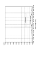
- FIG. 6 shows the result of measuring the shape of TSV present on the polished surface after polishing using a contact-type step gauge.
- the TSV having a diameter of 40 ⁇ m is a shape protruding from the main surface of the semiconductor substrate by about 0.08 ⁇ m, and it was confirmed that the difference in height between the semiconductor substrate and the TSV was small.
- the above shape was obtained by polishing using a CMP polishing liquid because of the effect of a combination of a CMP polishing liquid containing a predetermined component and a relatively hard polishing cloth having a Shore D hardness of 30 to 90. It is considered large.
Landscapes
- Chemical & Material Sciences (AREA)
- Organic Chemistry (AREA)
- Engineering & Computer Science (AREA)
- Materials Engineering (AREA)
- Mechanical Treatment Of Semiconductor (AREA)
- Finish Polishing, Edge Sharpening, And Grinding By Specific Grinding Devices (AREA)
Abstract
Priority Applications (1)
| Application Number | Priority Date | Filing Date | Title |
|---|---|---|---|
| KR1020137029047A KR20130135384A (ko) | 2011-06-01 | 2012-03-28 | Cmp 연마액 및 반도체 기판의 연마 방법 |
Applications Claiming Priority (2)
| Application Number | Priority Date | Filing Date | Title |
|---|---|---|---|
| JP2011123567 | 2011-06-01 | ||
| JP2011-123567 | 2011-06-01 |
Publications (1)
| Publication Number | Publication Date |
|---|---|
| WO2012165016A1 true WO2012165016A1 (fr) | 2012-12-06 |
Family
ID=47258882
Family Applications (1)
| Application Number | Title | Priority Date | Filing Date |
|---|---|---|---|
| PCT/JP2012/058187 Ceased WO2012165016A1 (fr) | 2011-06-01 | 2012-03-28 | Liquide de polissage mécano-chimique, et procédé de polissage de substrat semi-conducteur |
Country Status (4)
| Country | Link |
|---|---|
| JP (1) | JPWO2012165016A1 (fr) |
| KR (1) | KR20130135384A (fr) |
| TW (1) | TW201249975A (fr) |
| WO (1) | WO2012165016A1 (fr) |
Cited By (7)
| Publication number | Priority date | Publication date | Assignee | Title |
|---|---|---|---|---|
| JP2015171748A (ja) * | 2014-03-12 | 2015-10-01 | 株式会社ディスコ | 加工方法 |
| WO2016143323A1 (fr) * | 2015-03-11 | 2016-09-15 | 株式会社フジミインコーポレーテッド | Composition pour meulage et procédé pour le meulage d'un substrat en silicium |
| WO2019058815A1 (fr) * | 2017-09-20 | 2019-03-28 | ソニーセミコンダクタソリューションズ株式会社 | Capteur de détection de charge et système de mesure de potentiel |
| KR102410845B1 (ko) * | 2021-01-08 | 2022-06-22 | 에스케이씨솔믹스 주식회사 | 반도체 공정용 조성물 및 이를 이용한 반도체 소자 제조방법 |
| WO2023032028A1 (fr) * | 2021-08-31 | 2023-03-09 | 株式会社レゾナック | Liquide de polissage, procédé de polissage, procédé de fabrication de composant semi-conducteur, et procédé de fabrication de corps lié |
| JPWO2023032930A1 (fr) * | 2021-08-31 | 2023-03-09 | ||
| JP2023104444A (ja) * | 2022-01-18 | 2023-07-28 | 株式会社ディスコ | 被加工物の加工方法 |
Families Citing this family (2)
| Publication number | Priority date | Publication date | Assignee | Title |
|---|---|---|---|---|
| US11289387B2 (en) * | 2020-07-31 | 2022-03-29 | Applied Materials, Inc. | Methods and apparatus for backside via reveal processing |
| WO2025088991A1 (fr) * | 2023-10-24 | 2025-05-01 | 株式会社Sumco | Procédé de polissage de tranche de silicium |
Citations (7)
| Publication number | Priority date | Publication date | Assignee | Title |
|---|---|---|---|---|
| JP2004153086A (ja) * | 2002-10-31 | 2004-05-27 | Showa Denko Kk | 金属研磨組成物、金属膜の研磨方法および基板の製造方法 |
| JP2005007520A (ja) * | 2003-06-19 | 2005-01-13 | Nihon Micro Coating Co Ltd | 研磨パッド及びその製造方法並びに研磨方法 |
| WO2008156054A1 (fr) * | 2007-06-20 | 2008-12-24 | Asahi Glass Co., Ltd. | Composition de polissage et procédé de fabrication d'un dispositif de circuit intégré à semi-conducteur |
| JP2010082708A (ja) * | 2008-09-29 | 2010-04-15 | Fujibo Holdings Inc | 研磨パッド |
| JP2010082707A (ja) * | 2008-09-29 | 2010-04-15 | Fujibo Holdings Inc | 研磨パッド |
| JP2010245091A (ja) * | 2009-04-01 | 2010-10-28 | Fujifilm Corp | 化学的機械的研磨液及び研磨方法 |
| WO2010122985A1 (fr) * | 2009-04-20 | 2010-10-28 | 日立化成工業株式会社 | Liquide de polissage pour substrat semi-conducteur et procédé de polissage d'un substrat semi-conducteur |
-
2012
- 2012-03-28 WO PCT/JP2012/058187 patent/WO2012165016A1/fr not_active Ceased
- 2012-03-28 KR KR1020137029047A patent/KR20130135384A/ko not_active Ceased
- 2012-03-28 JP JP2013517903A patent/JPWO2012165016A1/ja active Pending
- 2012-05-02 TW TW101115568A patent/TW201249975A/zh unknown
Patent Citations (7)
| Publication number | Priority date | Publication date | Assignee | Title |
|---|---|---|---|---|
| JP2004153086A (ja) * | 2002-10-31 | 2004-05-27 | Showa Denko Kk | 金属研磨組成物、金属膜の研磨方法および基板の製造方法 |
| JP2005007520A (ja) * | 2003-06-19 | 2005-01-13 | Nihon Micro Coating Co Ltd | 研磨パッド及びその製造方法並びに研磨方法 |
| WO2008156054A1 (fr) * | 2007-06-20 | 2008-12-24 | Asahi Glass Co., Ltd. | Composition de polissage et procédé de fabrication d'un dispositif de circuit intégré à semi-conducteur |
| JP2010082708A (ja) * | 2008-09-29 | 2010-04-15 | Fujibo Holdings Inc | 研磨パッド |
| JP2010082707A (ja) * | 2008-09-29 | 2010-04-15 | Fujibo Holdings Inc | 研磨パッド |
| JP2010245091A (ja) * | 2009-04-01 | 2010-10-28 | Fujifilm Corp | 化学的機械的研磨液及び研磨方法 |
| WO2010122985A1 (fr) * | 2009-04-20 | 2010-10-28 | 日立化成工業株式会社 | Liquide de polissage pour substrat semi-conducteur et procédé de polissage d'un substrat semi-conducteur |
Cited By (13)
| Publication number | Priority date | Publication date | Assignee | Title |
|---|---|---|---|---|
| US11040427B2 (en) | 2014-03-12 | 2021-06-22 | Disco Corporation | Workpiece processing method |
| JP2015171748A (ja) * | 2014-03-12 | 2015-10-01 | 株式会社ディスコ | 加工方法 |
| WO2016143323A1 (fr) * | 2015-03-11 | 2016-09-15 | 株式会社フジミインコーポレーテッド | Composition pour meulage et procédé pour le meulage d'un substrat en silicium |
| US11754610B2 (en) | 2017-09-20 | 2023-09-12 | Sony Semiconductor Solutions Corporation | Charge detection sensor and potential measurement system |
| WO2019058815A1 (fr) * | 2017-09-20 | 2019-03-28 | ソニーセミコンダクタソリューションズ株式会社 | Capteur de détection de charge et système de mesure de potentiel |
| US12163992B2 (en) | 2017-09-20 | 2024-12-10 | Sony Semiconductor Solutions Corporation | Charge detection sensor and potential measurement system |
| KR102410845B1 (ko) * | 2021-01-08 | 2022-06-22 | 에스케이씨솔믹스 주식회사 | 반도체 공정용 조성물 및 이를 이용한 반도체 소자 제조방법 |
| WO2023032028A1 (fr) * | 2021-08-31 | 2023-03-09 | 株式会社レゾナック | Liquide de polissage, procédé de polissage, procédé de fabrication de composant semi-conducteur, et procédé de fabrication de corps lié |
| JPWO2023032930A1 (fr) * | 2021-08-31 | 2023-03-09 | ||
| WO2023032930A1 (fr) * | 2021-08-31 | 2023-03-09 | 株式会社レゾナック | Liquide de polissage, procédé de polissage, procédé de fabrication de composant, et procédé de fabrication de composant semi-conducteur |
| EP4379780A4 (fr) * | 2021-08-31 | 2024-12-25 | Resonac Corporation | Liquide de polissage, procédé de polissage, procédé de fabrication de composant, et procédé de fabrication de composant semi-conducteur |
| JP7750295B2 (ja) | 2021-08-31 | 2025-10-07 | 株式会社レゾナック | 研磨液、研磨方法、部品の製造方法、及び、半導体部品の製造方法 |
| JP2023104444A (ja) * | 2022-01-18 | 2023-07-28 | 株式会社ディスコ | 被加工物の加工方法 |
Also Published As
| Publication number | Publication date |
|---|---|
| JPWO2012165016A1 (ja) | 2015-02-23 |
| KR20130135384A (ko) | 2013-12-10 |
| TW201249975A (en) | 2012-12-16 |
Similar Documents
| Publication | Publication Date | Title |
|---|---|---|
| WO2012165016A1 (fr) | Liquide de polissage mécano-chimique, et procédé de polissage de substrat semi-conducteur | |
| KR101330956B1 (ko) | Cmp 연마액 및 연마 방법 | |
| JP4494538B2 (ja) | 銅系基板に有用な化学的・機械的研磨用スラリー | |
| KR101263625B1 (ko) | Cmp용 연마액 및 연마방법 | |
| JP3899456B2 (ja) | 研磨用組成物およびそれを用いた研磨方法 | |
| TWI453272B (zh) | 研磨液 | |
| TWI837097B (zh) | 鎢之化學機械拋光方法 | |
| CN106661382B (zh) | 化学机械抛光(cmp)组合物 | |
| JP6734854B2 (ja) | コバルト及び/又はコバルト合金含有の基板の研磨のための化学機械研磨(cmp)組成物の使用 | |
| TWI758254B (zh) | 化學機械研磨用組成物及化學機械研磨方法 | |
| TW201139633A (en) | Aqueous dispersion for chemical mechanical polishing, chemical mechanical polishing method using same, and kit for preparing aqueous dispersion for chemical mechanical polishing | |
| TW201629168A (zh) | 用於硏磨含有鈷及/或鈷合金的基板的化學機械硏磨(cmp)組成物的用途 | |
| TWI629324B (zh) | 研磨基板之方法 | |
| KR101273705B1 (ko) | Cmp 연마액 및 이 cmp 연마액을 사용한 기판의 연마 방법 | |
| JP2012182299A (ja) | 半導体基板用研磨液及び半導体基板の研磨方法 | |
| TW201333128A (zh) | 化學機械拋光液 | |
| US8845915B2 (en) | Abrading agent and abrading method | |
| TWI413679B (zh) | 研磨液 | |
| WO2018058347A1 (fr) | Polissage mécanochimique du tungstène à l'aide d'un procédé et d'une composition faisant appel à des composés de phosphonium quaternaire | |
| TWI752013B (zh) | 具有包含金屬之層的研磨對象物之研磨用組成物、研磨用組成物之製造方法、研磨方法、及基板之製造方法 | |
| JP2018157164A (ja) | 研磨用組成物、研磨用組成物の製造方法、研磨方法および半導体基板の製造方法 | |
| TW201821581A (zh) | 化學機械研磨方法及化學機械研磨用組成物 | |
| JPWO2011077973A1 (ja) | 銅研磨用研磨剤及びそれを用いた研磨方法 | |
| JP2004039673A (ja) | 研磨装置、研磨方法、および半導体装置の製造方法 | |
| JP2013004670A (ja) | 金属用研磨液及び金属用研磨液を用いた研磨方法 |
Legal Events
| Date | Code | Title | Description |
|---|---|---|---|
| 121 | Ep: the epo has been informed by wipo that ep was designated in this application |
Ref document number: 12792263 Country of ref document: EP Kind code of ref document: A1 |
|
| ENP | Entry into the national phase |
Ref document number: 2013517903 Country of ref document: JP Kind code of ref document: A |
|
| ENP | Entry into the national phase |
Ref document number: 20137029047 Country of ref document: KR Kind code of ref document: A |
|
| NENP | Non-entry into the national phase |
Ref country code: DE |
|
| 122 | Ep: pct application non-entry in european phase |
Ref document number: 12792263 Country of ref document: EP Kind code of ref document: A1 |