WO2012165156A1 - Dispositif de capture d'image radiologique - Google Patents
Dispositif de capture d'image radiologique Download PDFInfo
- Publication number
- WO2012165156A1 WO2012165156A1 PCT/JP2012/062624 JP2012062624W WO2012165156A1 WO 2012165156 A1 WO2012165156 A1 WO 2012165156A1 JP 2012062624 W JP2012062624 W JP 2012062624W WO 2012165156 A1 WO2012165156 A1 WO 2012165156A1
- Authority
- WO
- WIPO (PCT)
- Prior art keywords
- radiation
- absorbing
- scintillator
- image
- light
- Prior art date
- Legal status (The legal status is an assumption and is not a legal conclusion. Google has not performed a legal analysis and makes no representation as to the accuracy of the status listed.)
- Ceased
Links
Images


Classifications
-
- G—PHYSICS
- G01—MEASURING; TESTING
- G01T—MEASUREMENT OF NUCLEAR OR X-RADIATION
- G01T1/00—Measuring X-radiation, gamma radiation, corpuscular radiation, or cosmic radiation
- G01T1/16—Measuring radiation intensity
- G01T1/20—Measuring radiation intensity with scintillation detectors
- G01T1/2018—Scintillation-photodiode combinations
- G01T1/20188—Auxiliary details, e.g. casings or cooling
- G01T1/20189—Damping or insulation against damage, e.g. caused by heat or pressure
-
- G—PHYSICS
- G01—MEASURING; TESTING
- G01T—MEASUREMENT OF NUCLEAR OR X-RADIATION
- G01T1/00—Measuring X-radiation, gamma radiation, corpuscular radiation, or cosmic radiation
- G01T1/16—Measuring radiation intensity
- G01T1/20—Measuring radiation intensity with scintillation detectors
- G01T1/2018—Scintillation-photodiode combinations
- G01T1/20188—Auxiliary details, e.g. casings or cooling
- G01T1/2019—Shielding against direct hits
-
- A—HUMAN NECESSITIES
- A61—MEDICAL OR VETERINARY SCIENCE; HYGIENE
- A61B—DIAGNOSIS; SURGERY; IDENTIFICATION
- A61B6/00—Apparatus or devices for radiation diagnosis; Apparatus or devices for radiation diagnosis combined with radiation therapy equipment
- A61B6/42—Arrangements for detecting radiation specially adapted for radiation diagnosis
- A61B6/4283—Arrangements for detecting radiation specially adapted for radiation diagnosis characterised by a detector unit being housed in a cassette
-
- A—HUMAN NECESSITIES
- A61—MEDICAL OR VETERINARY SCIENCE; HYGIENE
- A61B—DIAGNOSIS; SURGERY; IDENTIFICATION
- A61B6/00—Apparatus or devices for radiation diagnosis; Apparatus or devices for radiation diagnosis combined with radiation therapy equipment
- A61B6/42—Arrangements for detecting radiation specially adapted for radiation diagnosis
- A61B6/4291—Arrangements for detecting radiation specially adapted for radiation diagnosis the detector being combined with a grid or grating
-
- G—PHYSICS
- G03—PHOTOGRAPHY; CINEMATOGRAPHY; ANALOGOUS TECHNIQUES USING WAVES OTHER THAN OPTICAL WAVES; ELECTROGRAPHY; HOLOGRAPHY
- G03B—APPARATUS OR ARRANGEMENTS FOR TAKING PHOTOGRAPHS OR FOR PROJECTING OR VIEWING THEM; APPARATUS OR ARRANGEMENTS EMPLOYING ANALOGOUS TECHNIQUES USING WAVES OTHER THAN OPTICAL WAVES; ACCESSORIES THEREFOR
- G03B42/00—Obtaining records using waves other than optical waves; Visualisation of such records by using optical means
- G03B42/02—Obtaining records using waves other than optical waves; Visualisation of such records by using optical means using X-rays
- G03B42/04—Holders for X-ray films
Definitions
- the present invention relates to a radiation imaging apparatus for capturing a radiation image.
- the radiation imaging system for imaging a subject (a region to be imaged by a patient) using radiation (for example, X-rays) to perform image diagnosis.
- the radiation imaging system has a radiation generating device for emitting radiation and a radiation imaging device for capturing a radiation image of an imaging region.
- the radiation imaging apparatus includes a stationary type incorporated in a standing position imaging table or a reclining position imaging table, and a portable type that can be carried (so-called electronic cassette).
- a portable radiographic imaging device can be inserted under the patient sleeping on a bed in a hospital room or the like and imaged.
- an FPD flat panel detector
- the FPD detects a radiation image by accumulating signal charges for each pixel on the detection surface, and outputs this as digital image data.
- FPD a direct conversion type FPD that converts radiation directly into signal charge in a conversion layer made of amorphous selenium (a-Se) or the like, and an indirect conversion that converts radiation once into visible light and converts visible light into signal charge Type FPD is known.
- the indirect type FPD is composed of a scintillator that converts radiation into visible light, a detection panel disposed opposite to the scintillator, and an electrical control circuit.
- the detection panel has a detection surface in which a photoelectric conversion unit that generates a signal charge by photoelectric conversion is formed for each pixel, converts visible light from the scintillator into a signal charge, and stores the signal charge.
- a TFT panel in which TFTs (thin-film transistors) and photoelectric conversion parts are arranged in a matrix on a glass substrate, or a CMOS image sensor (hereinafter referred to as a CMOS sensor) is used.
- the TFT is formed of an amorphous semiconductor such as amorphous silicon (a-Si).
- a-Si amorphous silicon
- photoelectric conversion parts and MOS transistors are formed in a matrix on a single crystal semiconductor substrate of silicon (Si) by a semiconductor process.
- the MOS transistor of the CMOS sensor is formed of a single crystal semiconductor, its carrier mobility is three to four orders of magnitude higher than that of a TFT panel formed of an amorphous semiconductor, enabling high-speed readout of signal charges. is there.
- the variation of characteristics for example, the threshold voltage of the MOS transistor and the like
- the CMOS sensor is suitable for moving image shooting and high-quality shooting.
- CMOS sensors can now be manufactured using a 12 inch wafer, with one side of the square having a size of about 200 mm. Therefore, for example, an FPD having a size of 17 inches, which is generally used for medical use, can be configured using four CMOS sensors.
- the radiation image capturing apparatus is set under the patient A protective structure for preventing damage in the case is required, and the radiographic imaging device becomes large.
- Japanese Patent Application Laid-Open No. 2005-249639 a scattered X-ray absorbing grid for absorbing X-rays scattered by a subject is disposed between the subject and the radiation imaging apparatus, and the outer periphery of the scattered X-ray absorbing grid is disposed What provided the absorption part which absorbs the X-ray irradiated to the blank area is disclosed. Further, Japanese Patent Application Laid-Open No. 2010-075553 discloses that a radiation generating apparatus is provided with a filter in which the amount of absorption of X-rays irradiated to the blank area is increased.
- both the absorbing unit described in JP-A-2005-249639 and the filter described in JP-A-2010-075553 absorb X-ray components necessary for imaging, and the image quality of the radiation image is degraded.
- neither JP-A-2005-249639 nor JP-A-2010-075553 describes the prevention of deterioration of the characteristics of the CMOS sensor and the prevention of damage.
- An object of the present invention is to provide a radiation image capturing apparatus capable of preventing characteristic deterioration of a radiation detector due to radiation and preventing damage due to a load or an impact from a subject.
- a radiation imaging device of the present invention is provided with a radiation detector and a radiation absorption part.
- the radiation detector detects radiation transmitted through the subject and generates image data.
- the radiation absorbing portion is disposed on the radiation incident side of the radiation detector, absorbs a part of the radiation incident on the radiation detector, and is deformable by the load of the subject.
- the radiation detector has a single crystal semiconductor substrate.
- the radiation absorbing portion has a bag and a liquid or gel radiation absorbing fluid sealed in the bag.
- a liquid scintillator that absorbs radiation and converts it into light may be used.
- a gelled water glass may be used as the radiation absorbing fluid.
- the radiation absorbing fluid may also have a liquid or gel fluid and a radiation absorbing material dispersed in the fluid.
- the radiation absorbing portion may have an elastic body which is deformed by a load from a subject, and a radiation absorbing material dispersed in the elastic body. Also, a plurality of radiation absorbing portions may be provided.
- the radiation detector has a scintillator that absorbs radiation and converts it into light, and a sensor panel that is disposed on the radiation irradiation side of the scintillator and that detects light converted by the scintillator.
- the radiation absorber preferably has a bag and a liquid scintillator enclosed in the bag.
- a signal output circuit includes a plurality of pixels including a photoelectric conversion layer that converts light converted by a scintillator into electric charge and a signal output circuit that outputs a signal according to the electric charge converted by the photoelectric conversion layer as a sensor panel Any of those provided over a single crystal semiconductor substrate can be used. As such a sensor panel, one configured by a CMOS type image sensor is used.
- the photoelectric conversion layer is preferably formed of amorphous silicon or quinacridone.
- the wavelength range of light generated by the liquid scintillator be different from the wavelength range of light detectable by the sensor panel.
- the radiation absorber is preferably larger in size than the radiation detector. It is preferable to include an image correction unit that corrects image data according to the area difference of the radiation absorption amount of the radiation absorption unit.
- the radiation absorbing portion preferably absorbs the low energy component of the radiation.
- the low energy component of the radiation absorbed by the radiation absorbing portion is an energy component of 1/2 or less of the energy distribution of the radiation.
- the radiation absorbing unit absorbs a part of the radiation, it is possible to suppress the characteristic deterioration of the radiation detector. Further, the radiation detector can be reinforced by the radiation absorbing portion to prevent damage to the radiation detector.
- the radiation absorbing portion is deformed by the load from the subject, the radiation absorption distribution is optimized according to the position, size, and range of the subject. As a result, the radiation transmitted through the subject does not deteriorate the image quality of the radiation image because the amount of radiation absorbed by the radiation absorbing portion is small, and the amount of radiation absorbed in the blank area directly irradiated with radiation is large, and the characteristics of the radiation detector deteriorate Is suppressed.
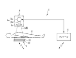
- a radiation imaging system 5 comprises: a radiation generator 6 for emitting X-rays as radiation toward the imaging region of a subject (patient) H; a radiation imaging apparatus 7 for imaging a radiation image of the subject H; A console 8 for controlling the radiation generator 6 and the radiation imaging device 7 is provided.
- the radiation generator 6 has a radiation source 6a and a source filter 6b.
- the radiation source 6a has an X-ray tube 6c for emitting X-rays and a radiation field limiter (collimator) 6d for limiting the radiation field of X-rays emitted by the X-ray tube 6c.
- the X-ray tube 6c has a cathode formed of a filament that emits thermoelectrons, and an anode (target) that emits thermorays which collide with the thermoelectrons emitted from the cathode.
- the irradiation field limiter 6d is, for example, a plurality of lead plates for shielding X-rays arranged on each side of a square and an irradiation opening for transmitting X-rays formed at the center, and the position of the lead plate is moved By changing the size of the irradiation opening, the irradiation field is limited.
- the radiation source filter 6b removes low energy components which are scattered when passing through the imaging region from the X-rays emitted from the radiation source 6a and cause deterioration of the radiation image.
- a material having a property of absorbing only the low energy component of the X-ray is used.
- aluminum is suitable.
- the high energy component of the X-ray transmitted through the radiation source filter 6 b is used for imaging the subject H.
- the energy distribution of the X-rays emitted from the X-ray tube 6c is, for example, approximately when the tube voltage of the X-ray tube 6c is 70 kV and the maximum energy of the X-rays emitted from the X-ray tube 6c is about 70 KeV 15 to 70 KeV.
- about 1/2 or less (15 to 40 KeV) of the energy distribution of the X-ray is a low energy component, and 1/2 or more (40 to 70 KeV) is a high energy component.
- the source filter 6b absorbs low energy components of 15 to 40 KeV.
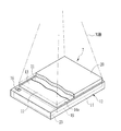
- the radiation image capturing apparatus 7 includes an FPD 19, a radiation absorbing unit 20, a light absorbing layer 21, an electric circuit unit 23, and a portable case 12.
- the housing 12 has a top plate 13 and a flat box-shaped housing body 14, and accommodates the FPD 19 and the electric circuit unit 23.
- the top plate 13 seals the opening 14 a at the top of the case body 14.
- the upper surface of the top plate 13 is an irradiation surface 11 to which X-rays emitted from the radiation generator 6 are irradiated.
- the top plate 13 is formed of carbon or the like having high X-ray permeability. Since carbon has high strength, it is suitable as a material of the top 13 to which the weight of the subject H is applied.
- the housing body 14 is formed of ABS resin or the like.
- the housing 12 is the same size (e.g., 17 inches by 17 inches) as a conventional radiation film cassette for recording a radiation image on a photosensitive material.
- the radiographic imaging device 7 has the same portability as the radiographic film cassette, and is used in place of the radiographic film cassette.
- the top plate 13 is provided with a display unit 16 configured of a plurality of LEDs.
- the display unit 16 displays an operation mode (e.g., "ready state” or “during data transmission” or the like) of the radiation imaging device 7 and an operation state such as a remaining capacity of a battery.
- the display unit 16 may be configured by a light emitting element other than an LED, a liquid crystal display, an organic EL display, or the like.
- the display unit 16 may be provided in the housing body 14.
- the light absorbing layer 21 and the radiation absorbing portion 20 are stacked in this order on the top plate 13.
- the radiation absorbing unit 20 faces the top 13 via the light absorbing layer 21.
- the radiation absorbing unit 20 absorbs a part of X-rays (for example, low energy components of X-rays) irradiated to the irradiation surface 11 and protects the FPD 19 from a load, an impact or the like applied to the top plate 13.
- the light absorbing layer 21 absorbs the light generated by the radiation absorbing unit 20 by the X-ray irradiation.
- the electric circuit unit 23 accommodates a signal processing unit 50, an image memory 51, a control unit 52, a wireless communication unit 53, a battery 54 and the like (all refer to FIG. 9).
- the electric circuit unit 23 is disposed at one end side along the short direction inside the housing 12.
- the FPD 19 operates by the power supplied from the battery 54.
- a radiation shielding member (not shown) such as a lead plate is provided on the top plate 13 side of the electric circuit section 23 in order to prevent the electric circuit section 23 from being damaged by X-rays.
- a light absorbing layer 21 is attached to the top surface of the top plate 13 with an adhesive (not shown).
- the radiation absorbing portion 20 is attached onto the light absorbing layer 21 by an adhesive (not shown).
- the light absorbing layer 21 and the radiation absorbing unit 20 cover the irradiation surface 11. Thereby, the radiation imaging device 7 can be thinned and the radiation detector 19 can be reinforced.
- the FPD 19 is one in which a sensor panel 25 and a scintillator 26 are sequentially stacked from the top 13 side along the direction in which the radiation is irradiated.
- a support substrate 27 supporting the scintillator 2 is provided on the lower surface of the scintillator 26.
- a sealing agent 28 is provided on the outer periphery of the FPD 19 in order to protect the scintillator 26 from moisture and the like.
- a drive circuit board 29 of the FPD 19 is disposed on the bottom of the housing 12. The drive circuit board 29 and the sensor panel 25 are electrically connected via the flexible cable 30.
- the scintillator 26 transmits the subject H and is irradiated to the irradiation surface 11 of the housing 12, and transmits the top plate 13, the radiation absorbing unit 20, and the sensor panel 25 to absorb incident X-rays and generate visible light.
- CsI: Tl cesium iodide to which thallium is added
- CsI: Na cesium iodide to which sodium is added
- GOS Gd 2 O 2 S: Tb
- CsI: Tl is used as the scintillator 26.
- the scintillator 26 is formed by vapor deposition of CsI: Tl on the support substrate 27.
- the scintillator 26 has a columnar crystal structure, and has a plurality of columnar crystals (not shown) along the direction from the support substrate 27 toward the sensor panel 25.
- the columnar crystal has a flat diameter substantially uniform along the longitudinal direction of the columnar crystal.
- the light generated by the scintillator 26 propagates in the columnar crystal due to the light guide effect of the columnar crystal, and is emitted toward the sensor panel 25 from the tip of the columnar crystal.
- the scintillator 26 in a columnar crystal structure, diffusion of visible light emitted from the scintillator 26 to the sensor panel 25 side is suppressed, so the sharpness of the radiation image captured by the radiation imaging device 7 Improve.
- a reflective layer (not shown) is provided on the surface of the support substrate 27 on the scintillator 26 side.
- the visible light emitted by the scintillator 26 and propagated to the support substrate 27 is reflected to the sensor panel 25 by the reflective layer, so the amount of light incident on the sensor panel 25 (detection efficiency of light emitted by the scintillator 26) is improved. Do.
- the configuration in which the sensor panel 25 is disposed on the X-ray incident side of the scintillator 26 is referred to as an ISS (Irradiation Side Sampling) method.
- a configuration in which the sensor panel is disposed on the opposite side to the X-ray incident side of the scintillator is called a PSS (Penetration Side Sampling) method.
- PSS Pulsion Side Sampling
- the sharpness and sensitivity of the radiation image are improved compared to the PSS method.
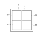
- the sensor panel 25 is configured by four CMOS type image sensors (hereinafter referred to as CMOS sensors) 33.
- CMOS sensors CMOS type image sensors
- Each CMOS sensor 33 has a plurality of pixels 33a (see FIG. 7) arranged in a matrix.
- Each CMOS sensor 33 has a rectangular shape with a side length of about 200 mm.
- the four CMOS sensors 33 are arranged adjacent to each other vertically and horizontally, and form a square of approximately 17 inches on a side.
- the CMOS sensor 33 has a configuration similar to that disclosed in U.S. Patent Publication 2009/0224162. Specifically, as shown in FIG. 5, the CMOS sensor 33 is constituted of a single crystal semiconductor substrate 34, an insulating layer 35, a first electrode 36, a photoelectric conversion layer 37, and a second electrode 38. There is.
- the single crystal semiconductor substrate 34 is made of single crystal Si.
- the insulating layer 35 is formed on the surface of the single crystal semiconductor substrate 34, and silicon oxide or the like is used for the insulating layer 35.
- the first electrode 36 is individually formed for each pixel 33 a on the surface of the insulating layer 35.
- the photoelectric conversion layer 37 is provided on the surface of each first electrode 36 in common to each pixel 33 a.
- the second electrode 38 is provided on the surface of the photoelectric conversion layer 37 in common to each pixel 33 a.
- the aforementioned scintillator 26 is bonded onto the surface of the second electrode 38 by an adhesive (not shown).
- the second electrode 38 is formed of a conductive material (for example, indium tin oxide (ITO)) which is transparent to visible light so that visible light generated by the scintillator 26 is incident on the photoelectric conversion layer 37.
- ITO indium tin oxide
- the second electrode 38 is provided in common to each pixel 33a, but may be provided individually for each pixel 33a.
- the photoelectric conversion layer 37 generates a signal charge according to the amount of incident X-rays, in combination with the scintillator 26.
- the photoelectric conversion layer 37 absorbs visible light generated by the scintillator 26, generates a signal charge according to the amount of absorbed light, and is formed of an organic or inorganic photoelectric conversion material.
- the inorganic photoelectric conversion material include amorphous silicon (a-Si).
- An example of the organic photoelectric conversion material is quinacridone.
- the sensitivity of the organic photoelectric conversion material (OPC) made of quinacridone is closer to the wavelength range of visible light generated by CsI: Tl than by CsI: Na or single crystal Si (c-Si). .
- CsI: Tl as the scintillator 26
- a signal output circuit 41 is provided for each pixel 33a.
- the signal output circuit 41 is formed of a CMOS circuit.
- the signal output circuit 41 and the first electrode 36 are electrically connected by the contact wiring 42.
- a bias voltage is applied to the second electrode 38 (see FIG. 7), and the signal charge generated by the photoelectric conversion layer 37 is collected by the first electrode 36 of each pixel 33 a.
- the signal output circuit 41 converts the signal charge collected by the first electrode 36 into a voltage signal corresponding to the signal charge amount and outputs the voltage signal.
- the signal output circuit 41 includes an output transistor T1, a row selection transistor T2, a reset transistor T3, a row selection line L1, a signal output line L2, and a reset line L3.
- the output transistor T1, the row selection transistor T2, and the reset transistor T3 are each a MOS transistor.
- the row selection line L1, the signal output line L2, and the reset line L3 are formed of a metal such as aluminum in the insulating layer 35 described above.
- the output transistor T1 is connected to the first electrode 36, and a voltage corresponding to the signal charge collected by the first electrode 36 is applied to the gate.
- the row selection transistor T2 is turned on by the selection signal applied to the row selection line L1, and a voltage signal controlled according to the gate voltage of the output transistor T1 is applied to the signal output line L2.
- the reset transistor T3 is turned on by the selection signal applied to the reset line L3, and discards the signal charge collected by the first electrode 36 to the power supply wiring Vdd.
- the carrier mobility of each of the transistors T1 to T3 is higher than that of a TFT made of an amorphous semiconductor such as a-Si.
- a control unit of the FPD 19 can be mixedly mounted on the single crystal semiconductor substrate 34.
- the row selection line L1, the signal output line L2, and the reset line L3 are formed of a metal such as aluminum, so there is little deterioration due to X-rays, but the output transistor T1, the row selection transistor T2, the reset Since the transistor T3 is formed of single crystal Si, there is a possibility that the characteristics may be degraded (change in threshold voltage or increase in dark current) due to X-rays. This is because in the MOS structure using single crystal Si, charges (hereinafter referred to as interface charge) are generated and accumulated at the interface between the single crystal semiconductor substrate 34 and the insulating layer 35 by absorption of X-rays.
- interface charge charges
- the radiation absorbing portion 20 absorbs a part of the X-rays transmitted through the top plate 13 (a low energy component affecting the characteristic deterioration of the MOS transistor).
- the high energy component of the X-ray passes through the CMOS sensor 33, but the low energy component of the X-ray does not have enough energy to pass through the CMOS sensor 33, and is absorbed by the CMOS sensor 33.
- the radiation absorbing portion 20 is composed of a bag 47 and a radiation absorbing fluid 48.
- the bag body 47 has elasticity that can be deformed by the load of the subject H.
- the radiation absorbing fluid 48 is enclosed in a bag 47.
- the bag body 47 is formed in a bag shape, for example, of an elastic material such as rubber or plastic material having a thickness of about several mm to 1 cm.
- the radiation absorbing fluid 48 is liquid or gel and has a property of absorbing a part of X-rays (low energy component). In the present embodiment, a liquid scintillator that absorbs X-rays and converts them into light is used as the radiation absorbing fluid 48.
- the liquid scintillator is formed of a solute composed of a phosphor, a solvent in which the solute is mixed, a surfactant, and the like.
- the properties of the liquid scintillator depend on the type and amount of solvent, solute, surfactant and the like.
- mixed xylene (isomer), toluene, pseudocumene, dioxane or the like is used as the solvent.
- solute for example, PPO, bulty-PBD, DMPOPOP, Bis-MSB or the like is used.
- the solution mass is, for example, 0.5 to 5 g / liter to construct a liquid scintillator.
- PPO is used as a solute, an emission spectrum of 440 nm or less is obtained. It is also possible to shift the emission spectrum to the long wave side by mixing a wavelength conversion material in the solute.
- the light absorbing layer 21 absorbs the light converted from the X-rays by the radiation absorbing unit 20 to prevent the light of the radiation absorbing unit 20 from being incident on the sensor panel 25. This prevents the image quality of the radiation image.
- the light absorption layer 21 is formed of a material capable of absorbing light emitted by the liquid scintillator.
- the imaging region of the subject H when the imaging region of the subject H is a hand, the imaging region is smaller than the imaging range of the FPD 19. Moreover, in such a case, the imaging region is mostly imaged in a state of being disposed at the center of the imaging range of the FPD 19. For this reason, the peripheral portion other than the central portion where the imaging region is arranged becomes a blank area where the X-rays are directly irradiated to the FPD 19, and characteristic deterioration easily occurs in the CMOS sensor 33.
- the X-ray incident on the FPD 19 has a small amount of X-ray absorption by the radiation absorbing portion 20 in the central portion that affects the image quality of the radiation image, and in the peripheral portion corresponding to one missing region Preferably, the amount of absorption is large.
- the radiation absorbing unit 20 can be deformed by the weight of the subject H. Specifically, as shown in FIG. 9, when the subject H is placed at the central portion of the radiation absorbing unit 20, the bag 47 is deformed by its weight, and the radiation absorbing fluid 48 is a bag. It flows in the bag 47 in accordance with the deformation of the body 47. As a result, in the radiation absorbing unit 20, the thickness of the central portion immediately below the subject H is reduced, and the thickness of the peripheral portion is increased.
- the X-ray intensity I after passing through the object is represented by the following equation (1), and decreases exponentially as the thickness T of the object increases when the attenuation coefficient ⁇ is constant. Therefore, when the radiation absorbing portion 20 is deformed as shown in FIG. 9, the X-ray absorption amount at the peripheral portion becomes high, so that the characteristic deterioration of the CMOS sensor 33 in the blank area is suppressed. Further, the amount of absorption of X-rays at the central portion of the radiation absorbing portion 20 is reduced, and the subject H is in a state of being close to the top 13, so X-ray scattering by the radiation absorbing portion 20 hardly occurs. Image quality deterioration is suppressed.
- I I'exp (- ⁇ T) (1)
- I X-ray intensity after transmission
- I ' X-ray intensity before transmission
- ⁇ Attenuation coefficient (different according to the type of substance and density)
- T Transmission thickness
- the single crystal semiconductor substrate 34 of the CMOS sensor 33 is easily broken in material and thin as about several tens of ⁇ m, it is preferable that the single crystal semiconductor substrate 34 have a protective structure that prevents damage due to the load of the object H applied to the top plate 13 .
- the sensor panel 25 configured of four CMOS sensors 33, when an impact or load is applied to the central portion of the sensor panel 25, all four CMOS sensors 33 may be damaged, and the repair cost is very high. large.
- the radiation absorbing portion 20 is deformed by the load from the subject H to absorb the load and the impact applied to the central portion of the top 13, so that the CMOS sensor 33 can be prevented from being damaged.
- the radiation absorbing unit 20 can suppress the heat of the subject H from being transmitted to the sensor panel 25, and can also suppress the image quality deterioration of the radiation image due to the temperature unevenness of the sensor panel 25.
- the electric circuit of the radiation image capturing apparatus 7 includes a sensor panel 25, a signal processing unit 50, an image memory 51, a control unit 52, a wireless communication unit 53, a battery 54 and the like.
- the signal processing unit 50 includes an amplifier for amplifying a pixel signal output from each pixel 33 a of the sensor panel 25, an A / D (analog / digital) converter, and the like, and the pixel signal output from the sensor panel 25 Into digital image data.
- the signal processing unit 50 further includes an image correction unit 50 a that corrects a radiation image according to the absorption distribution of low energy components of X-rays by the radiation absorption unit 20. Since the region to be imaged is mostly placed at the central portion, the central portion of the radiation absorbing unit 20 becomes thinner at the time of imaging, and the X absorption amount is smaller than that at the peripheral portion. The state of depression at the center depends on the imaging site. Therefore, the thickness of each part with respect to the imaging site is determined experimentally. Then, a correction coefficient for obtaining an X-ray absorption amount for each pixel or area corresponding to the thickness amount is set in the image correction unit 50a.
- the image correction unit 50a corrects the image data using the correction coefficient by designating the imaging region with the console 8, thereby removing the influence of the X-ray absorption amount of the radiation absorption unit 20.
- the accuracy of the correction can be improved by inputting the gender or the weight and the height.
- An image memory 51 is connected to the signal processing unit 50, and the image data output from the image correction unit 50 a of the signal processing unit 50 is stored in the image memory 51.
- the image memory 51 has a storage capacity capable of storing image data of a plurality of frames. Image data obtained by imaging is sequentially stored in the image memory 51 each time a radiographic image is captured.
- the control unit 52 includes a CPU 52a, a RAM 52b, and a ROM 52, and controls the overall operation of the radiation imaging device 7.
- the RAM 52 b is a temporary storage memory made of a DRAM or the like.
- the ROM 52 is a non-volatile memory including a flash memory or the like.
- the wireless communication unit 53 is an IEEE (Institute of Electrical and Electronics). Engineers) correspond to wireless LAN (Local Area Network) standards represented by 802.11a / b / g / n etc., and enable wireless communication of various information with external devices.
- the control unit 52 performs wireless communication with the console 8 via the wireless communication unit 53, and transmits and receives various types of information to and from the console 8.
- the battery 54 supplies power to each part in the radiation imaging device 7.
- the battery 54 is a rechargeable secondary battery, and is detachable from the radiation imaging device 7.
- the signal processing unit 50, the image memory 51, the control unit 52, and the wireless communication unit 53 may be provided in the drive circuit board 29. These are connected to one another via a bus.
- the console 8 includes a CPU 57, a ROM 58, a RAM 59, and an HDD 60, which are connected to one another via a bus 67.
- the CPU 57 controls each part of the console 8.
- the ROM 58 stores various programs including a control program.
- the RAM 59 temporarily stores various data.
- the HDD 60 stores various data.
- a communication I / F 61, a wireless communication unit 62, a display driver 64, and an operation input detection unit 66 are connected to the bus 67.
- a display 63 is connected to the display driver 64.
- An operation panel 65 is connected to the operation input detection unit 66.
- the communication I / F 61 is connected to the communication I / F 70 of the radiation generation device 6 via the connection terminal 61 a, the communication cable 69, and the connection terminal 70 a of the radiation generation device 6.
- the CPU 57 of the console 8 performs transmission and reception of various information such as the irradiation condition with the radiation generator 6 via the communication I / F 61.
- the wireless communication unit 62 has a function of performing wireless communication with the wireless communication unit 53 of the radiation image capturing apparatus 7.
- the CPU 57 of the console 8 exchanges various information such as image data with the radiation imaging device 7 via the wireless communication unit 62.
- the display driver 64 generates and outputs a signal for displaying various information on the display 63.
- the CPU 57 of the console 8 causes the display 63 to display the operation menu, the captured radiographic image, and the like via the display driver 64.
- the operation panel 65 has a plurality of keys, and can input various information and operation instructions.
- the operation input detection unit 66 detects an operation performed on the operation panel 65, and transmits the detection result to the CPU 57.
- the radiation generating apparatus 6 is configured of a communication I / F 70, a radiation source control unit 72, and a radiation source 6a.
- the communication I / F 70 transmits and receives various information such as an irradiation condition to and from the console 8.
- the radiation source control unit 72 controls the radiation source 6 a based on the irradiation conditions (including the information of the tube voltage and the tube current) received from the console 8.
- the photographer inserts the radiation imaging device 7 between the imaging region of the subject H and the imaging table with the irradiation surface 11 facing the imaging region.
- the orientation, position, and the like of the radiation imaging device 7 are finely adjusted.
- the radiation imaging device 7 when the imaging region is directly placed on the radiation imaging device 7, the radiation imaging device 7 is subjected to an impact or a load when mounting the imaging region.
- the impact and load are absorbed by deformation of the radiation absorbing portion 20.
- the radiation image capturing apparatus 7 of the present embodiment is an ISS method, and the sensor panel 25 is disposed on the top plate 13 side of the scintillator 26, so that breakage of the sensor panel 25 is effectively prevented.
- the photographer When the preparation work is completed, the photographer operates the operation panel 65 to instruct start of imaging.
- the console 8 transmits an instruction signal instructing the start of exposure to the radiation generator 6, and the radiation generator 6 causes the radiation source 6a to emit X-rays.
- the low energy component is absorbed by the radiation source filter 6b, the X-ray emitted from the radiation source 6a is transmitted through the imaging region of the subject H, and is irradiated to the irradiation surface 11 through the radiation absorbing portion 20 and the light absorbing layer 21. Ru.
- the X-rays pass through the top plate 13 and the sensor panel 25 and enter the scintillator 26.
- the low energy component of the X-rays transmitted through the object H is absorbed by the radiation absorbing unit 20, so that the characteristic deterioration of each CMOS sensor 33 due to the sensor panel 25 absorbing the X-rays is suppressed.
- the radiation absorbing portion 20 is deformed by the weight of the object H, and the thickness of the peripheral portion is thicker than that of the central portion. Therefore, the characteristic deterioration due to direct irradiation of the X-ray to the peripheral portion Is effectively suppressed.
- the radiation absorbing portion 20 has a central portion thinner than the peripheral portion, X-rays transmitted through the imaging region of the subject H are not absorbed more than necessary, and the image quality of the radiation image is greatly degraded. There is no.
- the X-rays incident on the scintillator 26 are converted into visible light in the vicinity of the X-ray incident surface of the scintillator 26, that is, on the sensor panel 25 side.
- the visible light generated by the scintillator 26 the visible light propagating toward the sensor panel 25 is incident on the sensor panel 25.
- the visible light propagated toward the support substrate 27 is reflected by the reflective layer of the support substrate 27 and then passes through the scintillator 26 again toward the sensor panel 25, and the sensor The light is incident on the panel 25. Since the visible light emitted by the scintillator 26 is guided by the columnar crystal made of CsI: Tl, image blurring is suppressed.
- the visible light incident on the scintillator 26 is transmitted through the second electrode 38 and incident on the photoelectric conversion layer 37, and is converted into signal charge by the photoelectric conversion layer 37.
- the signal charge generated in the photoelectric conversion layer 37 is collected by the first electrode 36 and converted to a voltage signal by the signal output circuit 41 after the end of the X-ray emission.
- This voltage signal is sequentially output from each pixel 33a as a pixel signal.
- the output pixel signals are converted into image data by the signal processing unit 50.
- the image data is corrected by the image correction unit 50a according to the amount of X-ray absorption which changes with the thickness of each portion of the radiation absorption unit 20.
- the image data after correction is stored in the image memory 51.
- the CPU 52 a transmits the image data stored in the image memory 51 to the console 8 via the wireless communication unit 53.
- the CPU 57 of the console 8 stores the image data received from the radiation imaging device 7 in the HDD 60 via the RAM 59. Further, the CPU 57 causes the display 63 to display a radiation image based on the image data stored in the HDD 60 via the display driver 64.
- the characteristic deterioration of the CMOS sensor 33 is suppressed.
- the radiation absorbing unit 20 is deformed according to the position of the subject H placed on the radiation imaging device 7, and the amount of absorption of the low energy component changes, so that the image quality of the radiation image is not deteriorated. Characteristic deterioration of the CMOS sensor 33 in the missing region is suppressed.
- the conventional ISS-type radiation imaging apparatus using a TFT panel is not easy to apply to mammography with a low tube voltage because the X-ray absorption of alkali-free glass used as a substrate of the TFT panel is large.
- a CMOS sensor with low X-ray absorption can be used for a radiation imaging apparatus of ISS method, application to mammography is easy.
- the light absorbing layer 21 is separately provided to absorb the light emitted from the radiation absorbing unit 20, but the light is applied to the bonding surface of the bag 47 with the top plate 13 or the entire bag 47. It may have absorbency.
- the wavelength range of the light emitted from the radiation absorbing fluid 48 may be different from the wavelength range detectable by the sensor panel 25 by appropriately selecting the type of solute or the wavelength conversion material. Thereby, the light absorption layer 21 can be omitted.
- a liquid scintillator is used as the radiation absorbing fluid 48, but a paraffin scintillator may be used.
- the paraffin scintillator is waxy at low temperature and has fluidity at about 40 ° C.
- the paraffin scintillator is described in detail in Japanese Patent Application Laid-Open No. 07-301676, so the detailed description is omitted.
- gelled water glass sodium silicate
- the gelation of water glass occurs, for example, by adding an acid to water glass and stirring.
- the radiation absorbing fluid 48 may be configured by dispersing an X-ray absorbing material in a liquid or gel fluid.
- an X-ray absorbing material metals of atomic numbers 20 to 31 (for example, copper) having a high effect of absorbing low energy components of X-rays and little back scattering are preferable.
- the radiation absorption part 20 is comprised with the bag body 47 and the radiation absorptive fluid body 48, you may form with elastic bodies, such as rubber
- the one radiation absorption part 20 is provided in the radiographic imaging apparatus 7, you may provide several radiation absorption parts.
- a plate-like low energy absorbing plate 75 for absorbing low energy components of X-rays is disposed between the top plate 13 and the sensor panel 25.
- the low energy absorbing plate 75 may be disposed between the top plate 13 and the radiation absorbing unit 20, or the low energy absorbing plate 75 may be used instead of the top plate 13.
- the low energy absorbing plate 75 for example, aluminum, glass or the like can be used, but the same material as the above-mentioned source filter 6b may be included.
- the transmitted X-ray energy distribution becomes the same.
- X-rays that can pass through the radiation source filter 6b are difficult to be absorbed by the radiation absorbing unit 20 as well, so that it is possible to suppress X-rays including information of the object H from being absorbed by the radiation absorbing unit 20. As a result, the utilization efficiency of X-rays is improved.
- the CMOS sensor may be configured by an organic thin film transistor formed on a plastic film so as to impart flexibility to the CMOS sensor.
- organic thin film transistors see “Tsuyoshi Sekitani, Flexible organic”. Since this is described in detail in “Transistors and circuits with extreme bending stability, Nature Materials 9, November 7, 2010, pp. 1015-1022”, the detailed description will be omitted.
- a photodiode and a transistor formed of single crystal Si may be provided over a flexible plastic substrate.
- a device block of about several tens of microns in size is dispersed in a solution, and FAS (Fluidic Self- Assembly) can be used.
- FSA Fluidic Self- Assembly
- “Koichi Maezawa” Resonant tunnel device block fabrication technology for Fluidic Self-Assembly ", Technical Report of IEICE, ED, Electronic Device, The Institute of Electronics, Information and Communication Engineers, 2008 6 May 6, 108, 87, p. Detailed description will be omitted as it is described in detail in 67-71.
- the sensor panel is constituted by a CMOS sensor, but the present invention is also applicable to a radiation image photographing apparatus in which the sensor panel is constituted by a CCD image sensor formed by a single crystal semiconductor substrate. .
- the present invention is not limited to the ISS method, and is also applicable to a PSS type radiation imaging apparatus.
- the present invention is also applicable to a direct conversion type radiation imaging apparatus that converts radiation directly into electric charges.
- the FPD is incorporated into a cassette-sized casing
- a standing-type or lying-down type imaging device or a mammography device it is also possible to be incorporated into a standing-type or lying-down type imaging device or a mammography device.
- the present invention is also applicable to a radiation imaging apparatus using radiation other than X-rays, such as ⁇ -rays.
- the configuration of the radiation image capturing apparatus according to the present invention described in the above embodiment is an example, and it goes without saying that the configuration can be appropriately changed without departing from the scope of the present invention.
Landscapes
- Physics & Mathematics (AREA)
- Health & Medical Sciences (AREA)
- Life Sciences & Earth Sciences (AREA)
- General Physics & Mathematics (AREA)
- High Energy & Nuclear Physics (AREA)
- Molecular Biology (AREA)
- Spectroscopy & Molecular Physics (AREA)
- Measurement Of Radiation (AREA)
- Apparatus For Radiation Diagnosis (AREA)
Abstract
L'invention concerne un dispositif de capture d'image radiologique (7) qui comprend un panneau de capteurs (25) constitué d'une pluralité de capteurs CMOS (33). Le panneau de capteurs (25) comprend un circuit de sortie de signal formé sur un substrat semi-conducteur monocristallin. La surface supérieure d'une plaque supérieure (13) exposée à des rayons X est équipée d'une unité absorbant le rayonnement (20) destinée à absorber certains des rayons X (composantes à basse énergie) responsables de la dégradation des caractéristiques du circuit de sortie de signal. L'unité absorbant le rayonnement (20) est constituée d'une poche (47) et d'un fluide absorbant le rayonnement (48) contenu dans la poche (47). L'unité absorbant le rayonnement (20) est déformée sous le chargement d'un sujet (H).
Applications Claiming Priority (2)
| Application Number | Priority Date | Filing Date | Title |
|---|---|---|---|
| JP2011-121967 | 2011-05-31 | ||
| JP2011121967A JP2012247402A (ja) | 2011-05-31 | 2011-05-31 | 放射線撮影装置 |
Publications (1)
| Publication Number | Publication Date |
|---|---|
| WO2012165156A1 true WO2012165156A1 (fr) | 2012-12-06 |
Family
ID=47259019
Family Applications (1)
| Application Number | Title | Priority Date | Filing Date |
|---|---|---|---|
| PCT/JP2012/062624 Ceased WO2012165156A1 (fr) | 2011-05-31 | 2012-05-17 | Dispositif de capture d'image radiologique |
Country Status (2)
| Country | Link |
|---|---|
| JP (1) | JP2012247402A (fr) |
| WO (1) | WO2012165156A1 (fr) |
Cited By (1)
| Publication number | Priority date | Publication date | Assignee | Title |
|---|---|---|---|---|
| CN108649004A (zh) * | 2018-05-21 | 2018-10-12 | 王青 | 一种光刻机用晶圆片涂胶系统 |
Families Citing this family (1)
| Publication number | Priority date | Publication date | Assignee | Title |
|---|---|---|---|---|
| JP6264723B2 (ja) * | 2013-01-23 | 2018-01-24 | コニカミノルタ株式会社 | 放射線画像撮影装置 |
Citations (10)
| Publication number | Priority date | Publication date | Assignee | Title |
|---|---|---|---|---|
| JPH05130990A (ja) * | 1991-10-25 | 1993-05-28 | Hamamatsu Photonics Kk | 自動露出機能付き医療用x線画像検出装置 |
| JPH0727864A (ja) * | 1993-07-14 | 1995-01-31 | Fuji Photo Film Co Ltd | 放射線検出器 |
| JPH11284909A (ja) * | 1998-01-28 | 1999-10-15 | Canon Inc | 二次元撮像装置 |
| JP2003035781A (ja) * | 2001-07-24 | 2003-02-07 | Canon Inc | 放射線画像撮影装置 |
| JP2004505252A (ja) * | 2000-07-21 | 2004-02-19 | トリクセル エス.アー.エス. | 耐用期間が伸びた放射線検出器 |
| JP2005506552A (ja) * | 2001-10-26 | 2005-03-03 | トリクセル エス.アー.エス. | 固体x線検出器 |
| JP2006058124A (ja) * | 2004-08-19 | 2006-03-02 | Canon Inc | カセッテ型x線画像撮影装置 |
| JP2007121100A (ja) * | 2005-10-27 | 2007-05-17 | Hitachi Ltd | 女性胸部の支持治具 |
| JP2009212377A (ja) * | 2008-03-05 | 2009-09-17 | Fujifilm Corp | 撮像素子及び撮像素子の製造方法 |
| JP2011095281A (ja) * | 2011-02-18 | 2011-05-12 | Konica Minolta Medical & Graphic Inc | 放射線画像検出器 |
-
2011
- 2011-05-31 JP JP2011121967A patent/JP2012247402A/ja not_active Withdrawn
-
2012
- 2012-05-17 WO PCT/JP2012/062624 patent/WO2012165156A1/fr not_active Ceased
Patent Citations (10)
| Publication number | Priority date | Publication date | Assignee | Title |
|---|---|---|---|---|
| JPH05130990A (ja) * | 1991-10-25 | 1993-05-28 | Hamamatsu Photonics Kk | 自動露出機能付き医療用x線画像検出装置 |
| JPH0727864A (ja) * | 1993-07-14 | 1995-01-31 | Fuji Photo Film Co Ltd | 放射線検出器 |
| JPH11284909A (ja) * | 1998-01-28 | 1999-10-15 | Canon Inc | 二次元撮像装置 |
| JP2004505252A (ja) * | 2000-07-21 | 2004-02-19 | トリクセル エス.アー.エス. | 耐用期間が伸びた放射線検出器 |
| JP2003035781A (ja) * | 2001-07-24 | 2003-02-07 | Canon Inc | 放射線画像撮影装置 |
| JP2005506552A (ja) * | 2001-10-26 | 2005-03-03 | トリクセル エス.アー.エス. | 固体x線検出器 |
| JP2006058124A (ja) * | 2004-08-19 | 2006-03-02 | Canon Inc | カセッテ型x線画像撮影装置 |
| JP2007121100A (ja) * | 2005-10-27 | 2007-05-17 | Hitachi Ltd | 女性胸部の支持治具 |
| JP2009212377A (ja) * | 2008-03-05 | 2009-09-17 | Fujifilm Corp | 撮像素子及び撮像素子の製造方法 |
| JP2011095281A (ja) * | 2011-02-18 | 2011-05-12 | Konica Minolta Medical & Graphic Inc | 放射線画像検出器 |
Cited By (1)
| Publication number | Priority date | Publication date | Assignee | Title |
|---|---|---|---|---|
| CN108649004A (zh) * | 2018-05-21 | 2018-10-12 | 王青 | 一种光刻机用晶圆片涂胶系统 |
Also Published As
| Publication number | Publication date |
|---|---|
| JP2012247402A (ja) | 2012-12-13 |
Similar Documents
| Publication | Publication Date | Title |
|---|---|---|
| JP5693173B2 (ja) | 放射線検出装置及び放射線検出システム | |
| CN103180757B (zh) | 放射线图像拍摄装置 | |
| US8742356B2 (en) | Radiation image detecting device | |
| JP6033363B2 (ja) | 放射線検出パネル | |
| JP5507415B2 (ja) | 放射線撮像装置 | |
| WO2012165155A1 (fr) | Dispositif d'imagerie radiographique | |
| JP2012247281A (ja) | 放射線撮影装置、及びシンチレータとその製造方法 | |
| JP5623316B2 (ja) | 放射線撮影装置及び製造方法 | |
| JPWO2013015016A1 (ja) | 放射線撮影装置 | |
| JP5624447B2 (ja) | 放射線検出装置及びシンチレータパネルの製造方法 | |
| US9006662B2 (en) | Radiological image detection device | |
| JP2012202735A (ja) | 放射線撮像装置 | |
| WO2012165156A1 (fr) | Dispositif de capture d'image radiologique | |
| JP2013011553A (ja) | 放射線撮影システム及び放射線撮影装置、並びに放射線撮影方法 | |
| JP2012093188A (ja) | 放射線検出パネル | |
| JP5638372B2 (ja) | 放射線画像撮影装置 | |
| JP2012200373A (ja) | 放射線撮影装置及び製造方法 | |
| JP5608533B2 (ja) | 放射線画像撮影装置 | |
| JP5666276B2 (ja) | 放射線画像撮影装置 | |
| JP5496938B2 (ja) | 放射線画像処理システム、プログラム及び欠陥画素補正方法 | |
| JP2012093259A (ja) | 放射線撮影装置 | |
| JP5608532B2 (ja) | 放射線画像撮影装置 | |
| WO2012029403A1 (fr) | Système d'imagerie par rayonnement, dispositif d'imagerie par rayonnement, et support d'enregistrement lisible à l'ordinateur | |
| WO2013015044A1 (fr) | Équipement radiographique | |
| JP2011227447A (ja) | 放射線画像撮影装置 |
Legal Events
| Date | Code | Title | Description |
|---|---|---|---|
| 121 | Ep: the epo has been informed by wipo that ep was designated in this application |
Ref document number: 12793139 Country of ref document: EP Kind code of ref document: A1 |
|
| NENP | Non-entry into the national phase |
Ref country code: DE |
|
| 122 | Ep: pct application non-entry in european phase |
Ref document number: 12793139 Country of ref document: EP Kind code of ref document: A1 |