WO2012165251A1 - Dispositif d'éclairage, dispositif d'affichage, et dispositif de réception de télévision - Google Patents
Dispositif d'éclairage, dispositif d'affichage, et dispositif de réception de télévision Download PDFInfo
- Publication number
- WO2012165251A1 WO2012165251A1 PCT/JP2012/063157 JP2012063157W WO2012165251A1 WO 2012165251 A1 WO2012165251 A1 WO 2012165251A1 JP 2012063157 W JP2012063157 W JP 2012063157W WO 2012165251 A1 WO2012165251 A1 WO 2012165251A1
- Authority
- WO
- WIPO (PCT)
- Prior art keywords
- light
- light source
- reflectance
- pair
- led
- Prior art date
- Legal status (The legal status is an assumption and is not a legal conclusion. Google has not performed a legal analysis and makes no representation as to the accuracy of the status listed.)
- Ceased
Links
Images









Classifications
-
- G—PHYSICS
- G02—OPTICS
- G02B—OPTICAL ELEMENTS, SYSTEMS OR APPARATUS
- G02B6/00—Light guides; Structural details of arrangements comprising light guides and other optical elements, e.g. couplings
- G02B6/0001—Light guides; Structural details of arrangements comprising light guides and other optical elements, e.g. couplings specially adapted for lighting devices or systems
- G02B6/0011—Light guides; Structural details of arrangements comprising light guides and other optical elements, e.g. couplings specially adapted for lighting devices or systems the light guides being planar or of plate-like form
- G02B6/0066—Light guides; Structural details of arrangements comprising light guides and other optical elements, e.g. couplings specially adapted for lighting devices or systems the light guides being planar or of plate-like form characterised by the light source being coupled to the light guide
- G02B6/0068—Arrangements of plural sources, e.g. multi-colour light sources
Definitions
- the present invention relates to a lighting device, a display device, and a television receiver.
- the display elements of image display devices such as television receivers are shifting from conventional cathode ray tubes to thin display panels such as liquid crystal panels and plasma display panels, which enables thinning of image display devices.
- a backlight device is separately required as a lighting device, and the backlight device is roughly classified into a direct type and an edge light type according to the mechanism.
- an edge light type backlight device it is preferable to use an edge light type backlight device, and an example described in Patent Document 1 below is known.
- An edge-light type backlight device may adopt a configuration in which a plurality of light sources are intermittently arranged in parallel along a light incident surface provided at an end portion of a light guide plate.
- the following problem may occur.
- the light quantity emitted from the plurality of light sources and incident on the light incident surface may be uneven due to the arrangement pattern and the non-arrangement pattern in the plurality of light sources intermittently arranged in parallel.
- the distance between the light source and the light incident surface is narrowed in order to narrow the frame of the liquid crystal display device and the backlight device, the above-described problem of unevenness tends to become more prominent.
- the present invention has been completed based on the above situation, and an object thereof is to suppress luminance unevenness.
- the illuminating device of the present invention is a surface parallel to the alignment direction of the plurality of light sources arranged in a row intermittently, and arranged in an opposing manner with a space between the light sources.
- a light guide plate having a light incident surface on which light from the light source is incident, a light output surface for emitting incident light, and a light output side of the light guide plate and the opposite side sandwich the light source.
- Low light with a relatively low light reflectivity which is arranged in accordance with the arrangement pattern of the light sources on a surface facing the light source in at least one of the pair of light source sandwiching portions and the pair of light source sandwiching portions
- a high-light-reflectance part with a relatively high light-reflectance part arranged following the non-arrangement pattern of the light source on a surface facing the light source in at least one of the reflectance part and the pair of light source sandwiching parts With.
- the light emitted from the plurality of light sources is propagated in the light guide plate after entering the light incident surface arranged in parallel with the light source arrangement direction and facing the light sources, The light exits from the light exit surface.
- the amount of light incident on the light incident surface of the light guide plate may be uneven due to the arrangement pattern and the non-arrangement pattern in the plurality of light sources arranged intermittently, and in particular, the narrow frame in the illumination device. If the distance between the light source and the light incident surface is narrowed in order to reduce the size, the occurrence of unevenness tends to become more prominent.
- the low light reflectance portion having a relatively low light reflectance is arranged following the light source arrangement pattern on the surface facing the light source in at least one of the pair of light source sandwiching portions.
- the high light reflectance portion having a relatively high light reflectance is arranged following the non-arrangement pattern of the light source, the arrangement pattern of the light source before the light from the light source enters the light incident surface. Reflection of light that tends to be excessive can be suppressed by the low light reflectance portion that follows the light source, while high efficiency of light reflection that tends to be insufficient is achieved by the high light reflectance portion that follows the non-arrangement pattern of the light source. be able to.
- the amount of light incident on the light incident surface of the light guide plate is made uniform regardless of the arrangement pattern and the non-arrangement pattern in the plurality of light sources arranged intermittently side by side, and unevenness hardly occurs.
- luminance unevenness is less likely to occur in the light emitted from the light exit surface of the light guide plate.
- this is also useful for narrowing the frame of the lighting device.
- the high light reflectance portion is arranged over the entire area of the non-arrangement pattern of the light source on the surface facing the light source in at least one of the pair of light source sandwiching portions. In this way, it is possible to further increase the efficiency of light reflection which tends to be insufficient due to the high light reflectance portion disposed over the entire area of the non-arrangement pattern of the light source. Thereby, luminance unevenness can be more effectively suppressed, and the overall light utilization efficiency and the luminance of the emitted light can be increased.
- the high light reflectance portion is arranged in a range from a non-light source pattern to an end portion of the light source arrangement pattern on a surface facing the light source in at least one of the pair of light source sandwiching portions.
- the low light reflectance portion is partially arranged in the light source arrangement pattern on the surface facing the light source in at least one of the pair of light source sandwiching portions.
- the overall light utilization efficiency and the luminance of the emitted light can be further increased.
- the light amount from the light source is relatively small at the end of the light source arrangement pattern compared to the central portion of the light source arrangement pattern. Therefore, the light is efficiently reflected by the high light reflectance portion at the end portion, which is suitable for further suppression of luminance unevenness.
- the low-light-reflectance part is arranged at least in the central part of the arrangement pattern of the light sources on the surface facing the light source in at least one of the pair of light source sandwiching parts.
- the amount of light from the light source is relative to the center of the light source arrangement pattern at the center of the light source arrangement pattern on the surface facing at least one of the pair of light source sandwiching portions as compared to the end of the light source arrangement pattern. Therefore, luminance unevenness can be more effectively suppressed by suppressing light reflection by the low light reflectance portion at the central portion.
- the low light reflectivity part and the high light reflectivity part are alternately arranged in the direction in which the light sources are arranged on a surface facing the light source in one of the pair of light source sandwiching parts. Yes. In this way, the amount of light incident on the light incident surface can be sufficiently uniformed by the low light reflectance portion and the high light reflectance portion disposed on the surface facing the light source in one of the pair of light source sandwiching portions. Can do. Compared to the case where the low light reflectivity part and the high light reflectivity part are arranged on both of the pair of light source sandwiching parts, it is possible to respond at a low cost and to suppress the reflection of light by the low light reflectivity part. Can be prevented from becoming excessive.
- the low light reflectivity part and the high light reflectivity part are arranged on the light source side of the pair of light source sandwiching parts arranged on the light emission side. In this way, after the light reflected by the low light reflectance portion and the high light reflectance portion is directed to the side opposite to the light emission side in the light source sandwiching portion disposed on the light emission side with respect to the light source. Reflected by the surface facing the light source in the light source sandwiching portion arranged on the side opposite to the light emitting side, or incident on the light incident surface and heading toward the surface of the light guide plate opposite to the light emitting side become. Accordingly, it is avoided that the reflected light from the low light reflectance portion and the high light reflectance portion is incident on the light incident surface and exits from the light exit surface as it is, so that luminance unevenness is more unlikely to occur in the emitted light.
- One of the pair of light source sandwiching portions is a pressing member that presses the light guide plate from the light emitting side.
- the light guide plate can be pressed from the light emission side as the pressing member is assembled, and the light source sandwiching portion of the pressing member can be arranged at an appropriate position with respect to the light source and the light guide plate. it can. Thereby, it is excellent in assembly workability.
- One of the pair of light source sandwiching portions is a chassis that houses the light source and the light guide plate. In this way, when the light source and the light guide plate are accommodated in the chassis, the light source and the light guide plate are arranged at appropriate positions with respect to the light source sandwiching portion of the chassis. Thereby, it is excellent in assembly workability.
- a reflective member is arranged along the direction in which the light sources are arranged in the pair of light source sandwiching portions, and at least one of the pair of light source sandwiching portions, the light source non-arrangement pattern An opening that overlaps at least a portion is formed, and the low light reflectance portion is configured by the light source sandwiching portion exposed through the opening, whereas the high light reflectance portion is configured by the reflecting member. ing. In this way, since the low light reflectance part and the high light reflectance part are configured by forming the opening in the reflecting member, compared with the case where it is possible to cope by performing printing etc. on the reflecting member, It can be handled at low cost.
- the pair of light source sandwiching portions is provided with a reflecting member along the arrangement direction of the light sources, and at least one of the pair of light source sandwiching portions has a relatively high light reflectance.
- a low-light-reflectance base material is included, and a high-light-reflectance material having a relatively high light reflectance is printed on a portion of the low-light-reflectance base material that overlaps at least part of the arrangement pattern of the light source It is configured to have a high light reflectance printing portion, and the high light reflectance printing portion is configured by the high light reflectance printing portion, whereas the high light reflectance printing portion is printed out of the low light reflectance substrate.
- the low light reflectance part is constituted by the non-printing part that is not performed.
- the low light reflectance part and the high light reflectance part are configured by printing the high light reflectance material on the low light reflectance base material to form the high light reflectance printing part.
- the mechanical strength of the reflecting member can be kept high as compared with the case where the opening is formed in the member.
- the pair of light source sandwiching portions is provided with a reflecting member along the arrangement direction of the light sources, and at least one of the pair of light source sandwiching portions has a relatively high light reflectance. It has a high high light reflectance base material, and a low light reflectance material having a relatively low light reflectance is printed on a portion of the high light reflectance base material that overlaps at least a part of the non-arrangement pattern of the light source.
- the low light reflectance printing unit is configured to have a low light reflectance printing unit, and the low light reflectance printing unit includes the low light reflectance printing unit, whereas the low light reflectance printing of the high light reflectance substrate.
- the high light reflectance part is constituted by a non-printing part on which no part is printed.
- the low light reflectance portion and the high light reflectance portion are configured by printing the low light reflectance material on the high light reflectance base material to form the low light reflectance printing portion.
- the mechanical strength of the reflecting member can be kept high as compared to the case where the opening is formed in the reflecting member.
- a display device of the present invention includes the above-described illumination device and a display panel that performs display using light from the illumination device.
- the illumination device that supplies light to the display panel is less likely to cause uneven brightness in the emitted light, it is possible to realize display with excellent display quality.
- a liquid crystal panel can be exemplified as the display panel.
- Such a display device can be applied as a liquid crystal display device to various uses such as a display of a television or a personal computer, and is particularly suitable for a large screen.
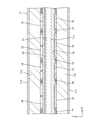
- FIG. 1 is an exploded perspective view showing a schematic configuration of a television receiver according to Embodiment 1 of the present invention.
- Exploded perspective view showing schematic configuration of liquid crystal display device Sectional drawing which shows the cross-sectional structure along the long side direction of a liquid crystal panel
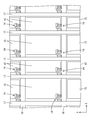
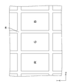
- the top view which shows arrangement
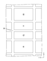
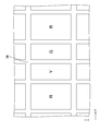
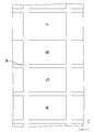
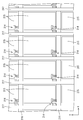
- Sectional drawing which shows the structure regarding the surface facing LED in the 1st light source clamping part which concerns on Embodiment 6 of this invention.
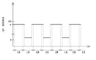
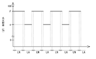
- the graph showing the change of the light reflectivity in the arrangement direction of LED of the surface facing LED in the 1st light source clamping part which concerns on Embodiment 7 of this invention.
- FIGS. 1 A first embodiment of the present invention will be described with reference to FIGS.
- the liquid crystal display device 10 is illustrated.
- a part of each drawing shows an X axis, a Y axis, and a Z axis, and each axis direction is drawn to be a direction shown in each drawing.
- the upper side shown in FIG. 7 be a front side, and let the lower side of the figure be a back side.
- the television receiver TV includes a liquid crystal display device 10 that is a display device, front and back cabinets Ca and Cb that are accommodated so as to sandwich the liquid crystal display device 10, and power supply.
- Power supply circuit board P a tuner (receiving unit) T capable of receiving a TV image signal, an image conversion circuit board VC for converting the TV image signal output from the tuner T into an image signal for the liquid crystal display device 10
- a stand S a stand S.
- the liquid crystal display device 10 has a horizontally long (longitudinal) rectangular shape (rectangular shape) as a whole, the long side direction is the horizontal direction (X-axis direction), and the short side direction is the vertical direction (Y-axis direction, vertical direction).
- the liquid crystal display device 10 includes a liquid crystal panel 11 that is a display panel and a backlight device (illumination device) 12 that is an external light source, which are integrated by a frame-like bezel 13 or the like. Is supposed to be retained.
- the configuration of the liquid crystal panel 11 in the liquid crystal display device 10 will be described.
- the liquid crystal panel 11 has a horizontally long (longitudinal) rectangular shape (rectangular shape) as a whole.
- a pair of transparent (translucent) glass substrates 11a and 11b And a liquid crystal layer 11c containing liquid crystal, which is a substance whose optical characteristics change with application of an electric field.
- the substrates 11a and 11b maintain a gap corresponding to the thickness of the liquid crystal layer. In the state, they are bonded together by a sealing agent (not shown).
- polarizing plates 11d and 11e are attached to the outer surface sides of both the substrates 11a and 11b, respectively. Note that the long side direction of the liquid crystal panel 11 coincides with the X-axis direction, and the short side direction coincides with the Y-axis direction.
- the front side is the CF substrate 11a
- the back side is the array substrate 11b.
- TFTs Thin Film Transistors
- pixel electrodes 15 which are switching elements are matrixed.
- a large number of gate wirings 16 and source wirings 17 are arranged around the TFTs 14 and the pixel electrodes 15 so as to surround the TFTs 14 and the pixel electrodes 15.
- the pixel electrode 15 has a vertically long (longitudinal) rectangular shape (rectangular shape) in which the long side direction coincides with the Y-axis direction and the short side direction coincides with the X-axis direction. It consists of a transparent electrode such as (Zinc Oxide).
- the gate wiring 16 and the source wiring 17 are connected to the gate electrode and the source electrode of the TFT 14, respectively, and the pixel electrode 15 is connected to the drain electrode of the TFT 14. Further, as shown in FIG. 3, an alignment film 18 for aligning liquid crystal molecules is provided on the TFT 14 and the pixel electrode 15 on the liquid crystal layer 11c side.
- a terminal portion led out from the gate wiring 16 and the source wiring 17 is formed at an end portion of the array substrate 11b, and a driver component for driving a liquid crystal (not shown) is connected to the anisotropic conductive film (not shown).
- ACF isotropic Conductive Film
- the driver component for driving the liquid crystal is electrically connected to a display control circuit board (not shown) via various wiring boards.
- This display control circuit board is connected to an image conversion circuit board VC (see FIG. 1) in the television receiver TV, and each wiring 16, 17 via a driver component based on an output signal from the image conversion circuit board VC. It is assumed that a drive signal is supplied to.
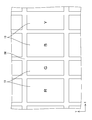
- a color filter 19 in which the portions R, G, B, and Y are arranged in a matrix (matrix) is provided.
- the color filter 19 according to the present embodiment includes a yellow colored portion Y in addition to a red colored portion R, a green colored portion G, and a blue colored portion B that are the three primary colors of light.
- the colored portions R, G, B, and Y selectively transmit light of each corresponding color (each wavelength).
- Each colored portion R, G, B, Y has a vertically long (longitudinal) rectangular shape (rectangular shape) in which the long side direction coincides with the Y-axis direction and the short side direction coincides with the X-axis direction, like the pixel electrode 15. I am doing.
- a lattice-shaped light shielding layer (black matrix) BM is provided to prevent color mixing.
- a counter electrode 20 and an alignment film 21 are sequentially stacked on the color filter 19 on the CF substrate 11 a on the liquid crystal layer 11 c side.
- the colored portions R, G, B, and Y constituting the color filter 19 will be described in detail.
- the colored portions R, G, B, and Y are arranged in a matrix with the X-axis direction as the row direction and the Y-axis direction as the column direction.
- Y have the same dimension in the column direction (Y-axis direction), but the dimension in the row direction (X-axis direction) is different for each colored portion R, G, B, Y.
- the colored portions R, G, B, and Y are arranged in the row direction in the order of the red colored portion R, the green colored portion G, the blue colored portion B, and the yellow colored portion Y from the left side shown in FIG.
- the red colored portion R and the blue colored portion B in the row direction are relatively larger than the yellow colored portion Y and the green colored portion G in the row direction. It is said. That is, the colored portions R and B having relatively large dimensions in the row direction and the colored portions G and Y having relatively small dimensions in the row direction are alternately and repeatedly arranged in the row direction. Thereby, the area of the red coloring part R and the blue coloring part B is made larger than the areas of the green coloring part G and the yellow coloring part Y. The areas of the blue colored portion B and the red colored portion R are equal to each other. Similarly, the areas of the green colored portion G and the yellow colored portion Y are equal to each other. 3 and 5 show a case where the areas of the red colored portion R and the blue colored portion B are about 1.6 times the areas of the yellow colored portion Y and the green colored portion G. Show.
- the dimension in the row direction (X-axis direction) of the pixel electrode 15 varies from column to column. . That is, among the pixel electrodes 15, the size and area in the row direction of the pixel electrode 15 that overlaps with the red color portion R and the blue color portion B are the same as those in the row direction of the pixel electrode 15 that overlaps with the yellow color portion Y and the green color portion G. It is relatively larger than the size and area.
- the gate wirings 16 are all arranged at an equal pitch, while the source wirings 17 are arranged at two different pitches depending on the dimensions of the pixel electrodes 15 in the row direction.
- the liquid crystal display device 10 uses the liquid crystal panel 11 including the color filter 19 including the four colored portions R, G, B, and Y, as shown in FIG.
- the television receiver TV is provided with a dedicated image conversion circuit board VC. That is, the image conversion circuit board VC converts the television image signal output from the tuner T into an image signal of each color of blue, green, red, and yellow, and outputs the generated image signal of each color to the display control circuit board. can do. Based on this image signal, the display control circuit board drives the TFTs 14 corresponding to the pixels of each color in the liquid crystal panel 11 via the wirings 16 and 17, and transmits the colored portions R, G, B, and Y of each color. The amount of light can be appropriately controlled.
- the backlight device 12 includes a chassis 22 having a substantially box shape having an opening (light emitting portion) that opens toward the front side (the liquid crystal panel 11 side), and an opening of the chassis 22. And a group of optical members 23 arranged in a covering manner. Further, in the chassis 22, an LED 24 that is a light source, an LED substrate 25 on which the LED 24 is mounted, a light guide plate 26 that guides light from the LED 24 and guides it to the optical member 23 (the liquid crystal panel 11), and a light guide. A frame (pressing member) 27 for pressing the optical plate 26 from the front side is provided.
- the backlight device 12 is a so-called edge light type (side light type) in which the LEDs 24 mounted on the LED substrate 25 are arranged at both ends of the light guide plate 26, respectively.
- the edge light type backlight device 12 is integrally assembled to the liquid crystal panel 11 by a bezel 13 having a frame shape, thereby constituting the liquid crystal display device 10.
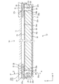
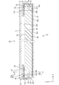
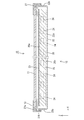
- the chassis 22 is made of metal, and includes a bottom plate 22a having a horizontally long rectangular shape as in the liquid crystal panel 11, and side plates 22b rising from the outer ends of the respective sides of the bottom plate 22a. As a whole, it has a shallow, generally box shape that opens toward the front side.
- the chassis 22 (bottom plate 22a) has a long side direction that matches the X-axis direction (horizontal direction), and a short side direction that matches the Y-axis direction (vertical direction). Further, the frame 27 and the bezel 13 can be screwed to the side plate 22b.
- the optical member 23 has a horizontally long rectangular shape in a plan view, like the liquid crystal panel 11 and the chassis 22.
- the optical member 23 is placed on the front side (light emitting side) of the light guide plate 26 and is interposed between the liquid crystal panel 11 and the light guide plate 26.
- the optical member 23 includes a diffusion plate 23a disposed on the back side and an optical sheet 23b disposed on the front side.
- the diffusing plate 23a has a structure in which a large number of diffusing particles are dispersed in a substrate made of a substantially transparent resin having a predetermined thickness and has a function of diffusing transmitted light.
- the optical sheet 23b has a sheet shape that is thinner than the diffusion plate 23a, and three optical sheets 23b are stacked. Specific types of the optical sheet 23b include, for example, a diffusion sheet, a lens sheet, a reflective polarizing sheet, and the like, which can be appropriately selected and used. 7 to 10, the illustration of the optical member 23 is simplified.
- the frame 27 is formed in a horizontally long frame shape (frame shape) extending along the outer peripheral edge portions of the optical member 23 and the light guide plate 26 as a whole.
- the outer peripheral edge of the light guide plate 26 can be pressed from the front side over the entire circumference.
- the frame 27 is made of a synthetic resin and has a light shielding property by having a surface with, for example, a black color.
- the frame 27 protrudes from the outer peripheral end of the pressing base 27a toward the back side and surrounds the side plate 22b of the chassis 22 from the outside (externally fitted). ) It is composed of a peripheral wall portion 27b that forms a short cylindrical shape.
- the holding base portion 27a has a pair of short side portions and long side portions, and a pair of long side portions of the holding base portion 27a and a pair of first light source sandwiching portions 27c sandwiching the LED 24 with the bottom plate 22a of the chassis 22; Is done.
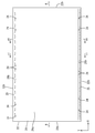
- the front side surfaces of the pair of first light source sandwiching portions 27c that is, the surfaces facing the LEDs 24 (the surfaces facing the LEDs 24, the surfaces receiving the light from the LEDs 24, and the surfaces exposed to the light from the LEDs 24) are shown in FIGS.
- a pair of first reflection sheets 28 that reflect light are respectively attached. In FIG. 11, the first reflection sheet 28 is shown in a shaded shape.
- the first reflection sheet 28 is made of a synthetic resin and has a white surface with excellent light reflectivity.
- the first reflection sheet 28 has a size that extends over almost the entire length of the long side portion (first light source sandwiching portion 27 c) of the frame 27, and is in direct contact with the end portion of the light guide plate 26 on the LED 24 side.
- the above-described end portion (the end portion having the light incident surface 26b) of the light guide plate 26 and the LED substrate 25 (including the LED 24) are collectively covered from the front side.
- the frame 27 can receive the outer peripheral end of the liquid crystal panel 11 from the back side. The detailed configuration of the first reflection sheet 28 will be described later.
- the LED 24 is mounted on the LED substrate 25 and is a so-called top type in which a surface opposite to the mounting surface with respect to the LED 25 is a light emitting surface.
- the LED 24 includes an LED chip that emits blue light as a light emission source, and includes a green phosphor and a red phosphor as phosphors that emit light when excited by blue light.
- the LED 24 has a configuration in which an LED chip made of, for example, an InGaN-based material is sealed with a resin material on a substrate portion fixed to the LED substrate 25.
- the LED chip mounted on the substrate part has a main emission wavelength in the range of 420 nm to 500 nm, that is, in the blue wavelength region, and can emit blue light (blue monochromatic light) with excellent color purity. Is done.
- a specific main emission wavelength of the LED chip for example, 451 nm is preferable.
- the resin material that seals the LED chip is excited by the blue phosphor emitted from the LED chip and the green phosphor that emits green light by being excited by the blue light emitted from the LED chip. And a red phosphor emitting red light is dispersed and blended at a predetermined ratio.
- the LED 24 is made up of blue light (blue component light) emitted from these LED chips, green light (green component light) emitted from the green phosphor, and red light (red component light) emitted from the red phosphor. Is capable of emitting light of a predetermined color as a whole, for example, white or blueish white. Since yellow light is obtained by synthesizing the green component light from the green phosphor and the red component light from the red phosphor, the LED 24 includes the blue component light and the yellow component from the LED chip. It can be said that it also has the light of.
- the chromaticity of the LED 24 varies depending on, for example, the absolute value or relative value of the content of the green phosphor and the red phosphor, and accordingly the content of the green phosphor and the red phosphor is adjusted as appropriate. Thus, the chromaticity of the LED 24 can be adjusted.
- the green phosphor has a main emission peak in the green wavelength region of 500 nm to 570 nm
- the red phosphor has a main emission peak in the red wavelength region of 600 nm to 780 nm. It is said.
- the green phosphor and the red phosphor provided in the LED 24 will be described in detail.
- ⁇ -SiAlON which is a kind of sialon phosphor
- the sialon-based phosphor is a substance in which a part of silicon atoms of silicon nitride is replaced with aluminum atoms and a part of nitrogen atoms with oxygen atoms, that is, a nitride.
- a sialon-based phosphor that is a nitride is superior in luminous efficiency and durability as compared with other phosphors made of, for example, sulfides or oxides.
- “excellent in durability” specifically means that, even when exposed to high-energy excitation light from an LED chip, the luminance does not easily decrease over time.
- rare earth elements eg, Tb, Yg, Ag, etc.
- ⁇ -SiAlON which is a kind of sialon-based phosphor, has a general formula Si6-zAlzOzN8-z: Eu (z indicates a solid solution amount) or (Si, Al) in which aluminum and oxygen are dissolved in ⁇ -type silicon nitride crystal. ) 6 (O, N) 8: A substance represented by Eu.
- the ⁇ -SiAlON for example, Eu (europium) is used as an activator, and thereby the color purity of green light, which is emitted light, is particularly high. It is extremely useful in adjusting On the other hand, as the red phosphor, it is preferable to use casoon, which is a kind of cascading phosphor.
- Cousin-based phosphors are nitrides containing calcium atoms (Ca), aluminum atoms (Al), silicon atoms (Si), and nitrogen atoms (N). For example, other phosphors made of sulfides, oxides, etc. In comparison, it is excellent in luminous efficiency and durability.
- the cascading phosphor uses rare earth elements (for example, Tb, Yg, Ag, etc.) as an activator.
- Casun which is a kind of cousin phosphor, uses Eu (europium) as an activator and is represented by the composition formula CaAlSiN3: Eu.
- the LED substrate 25 has an elongated plate shape extending along the long side direction of the chassis 22 (X-axis direction, the longitudinal direction of the light incident surface 26b of the light guide plate 26).
- the main plate surface is accommodated in the chassis 22 in a posture parallel to the X-axis direction and the Z-axis direction, that is, in a posture orthogonal to the plate surfaces of the liquid crystal panel 11 and the light guide plate 26 (optical member 23).
- the LED boards 25 are arranged in pairs corresponding to both ends on the long side in the chassis 22, and are attached to the inner surfaces of the side plates 22b on the long side.
- the LED 24 having the above-described configuration is surface-mounted on the main plate surface of the LED substrate 25 and on the inner side, that is, the surface facing the light guide plate 26 side (the surface facing the light guide plate 26).
- a plurality of LEDs 24 are arranged in a line (linearly) in parallel on the mounting surface of the LED substrate 25 along the length direction (X-axis direction) with a predetermined interval. That is, it can be said that a plurality of LEDs 24 are intermittently arranged in parallel along the long side direction at both ends on the long side of the backlight device 12.
- the arrangement direction of the LEDs 24 coincides with the length direction (X-axis direction) of the LED substrate 25.
- each LED 24 Since the pair of LED substrates 25 are housed in the chassis 22 in such a posture that the mounting surfaces of the LEDs 24 are opposed to each other, the light emitting surfaces of the LEDs 24 respectively mounted on the LED substrates 25 are opposed to each other, The optical axis of each LED 24 substantially coincides with the Y-axis direction.
- the base material of the LED substrate 25 is made of a metal such as an aluminum material same as that of the chassis 22, and a wiring pattern (not shown) made of a metal film such as a copper foil is formed on the surface thereof via an insulating layer.
- a wiring pattern (not shown) made of a metal film such as a copper foil is formed on the surface thereof via an insulating layer.
- the outermost surface is formed with a reflective layer (not shown) that exhibits white light with excellent light reflectivity.
- the LEDs 24 arranged in parallel on the LED substrate 25 are connected in series by this wiring pattern.
- insulating materials such as a ceramic.
- the light guide plate 26 is made of a synthetic resin material (for example, acrylic resin such as PMMA, polycarbonate, etc.) having a refractive index higher than air and substantially transparent (excellent translucency).
- the light guide plate 26 has a horizontally long rectangular shape as seen in a plan view like the liquid crystal panel 11 and the chassis 22, and the long side direction is the X axis direction and the short side direction. Respectively agree with the Y-axis direction.
- the light guide plate 26 is disposed in the chassis 22 immediately below the liquid crystal panel 11 and the optical member 23, and a pair of LED substrates 25 disposed at both ends of the long side of the chassis 22. The Y-axis direction is interposed between them.
- the alignment direction of the LED 24 (LED substrate 25) and the light guide plate 26 matches the Y-axis direction, while the alignment direction of the optical member 23 (liquid crystal panel 11) and the light guide plate 26 matches the Z-axis direction. It is assumed that both directions are orthogonal to each other.
- the light guide plate 26 introduces the light emitted from the LED 24 in the Y-axis direction, and rises and emits the light toward the optical member 23 side (Z-axis direction) while propagating the light inside.
- the light guide plate 26 has a substantially flat plate shape extending along the bottom plate 22 a of the chassis 22 and the plate surfaces of the optical member 23. It is assumed to be parallel to the Y-axis direction.
- the surface facing the front side is a light emitting surface 26 a that emits internal light toward the optical member 23 and the liquid crystal panel 11.
- both end surfaces on the long side that are long in the X-axis direction, that is, along the direction in which the LEDs 24 are arranged, are respectively connected to the LED 24 (LED substrate 25) and a predetermined length.
- Each light incident surface 26b is a surface parallel to the X-axis direction (alignment direction of the LEDs 24) and the Z-axis direction, that is, the main plate surface of the LED substrate 25, and is a surface substantially orthogonal to the light emitting surface 26a.
- the alignment direction of the LED 24 and the light incident surface 26b coincides with the Y-axis direction and is parallel to the light emitting surface 26a.
- a predetermined space is held between the light incident surface 26 b of the light guide plate 26 and the LED 24, and a portion of the bottom plate 22 a of the chassis 22 facing the space, that is, on the frame 27 side.
- the portion that sandwiches the LED 24 with the first light source sandwiching portion 27c is the second light source sandwiching portion 22c.
- a pair of the second light source sandwiching portions 22c is arranged according to the arrangement of the pair of first light source sandwiching portions 27c and the pair of LEDs 24 (LED substrate 25). Light is reflected on the surface on the front side of the pair of second light source sandwiching portions 22c, that is, the surface facing the LED 24 (the surface facing the LED 24, the surface receiving the light from the LED 24, the surface exposed to the light from the LED 24).
- a pair of second reflection sheets 29 are respectively attached. That is, the space held between the LED 24 and the LED 24 and the light incident surface 26b includes the first reflection sheet 28 arranged on the front side (light emission side of the light guide plate 26) and the back side (light emission of the light guide plate 26). Sandwiched between the second reflection sheet 29 disposed on the opposite side). As a result, the light emitted from the LED 24 is repeatedly reflected between the reflecting sheets 28 and 29, and thus efficiently enters the light incident surface 26b.
- the second reflection sheet 29 is made of a synthetic resin, like the first reflection sheet 28, and has a white surface with excellent light reflectivity. Further, the second reflection sheet 29 has a size capable of sandwiching the end portion having the light incident surface 26b of the LED substrate 25 and the light guide plate 26 in addition to the LED 24 with the first reflection sheet 28. Have.
- the surface of the light guide plate 26 opposite to the light output surface 26a (the surface facing the bottom plate 22a of the chassis 22 and the surface received by the bottom plate 22a of the chassis 22) 26c reflects the light in the light guide plate 26 to the front side.
- a light guide reflection sheet 30 that can be raised is provided so as to cover the entire area.
- the light guide reflection sheet 30 is disposed between the bottom plate 22 a of the chassis 22 and the light guide plate 26.
- the light guide reflection sheet 30 is made of a synthetic resin, like the first reflection sheet 28 and the second reflection sheet 29 described above, and has a white surface with excellent light reflectivity.
- At least one of the light exit surface 26a and the opposite surface 26c of the light guide plate 26 has a reflection part (not shown) for reflecting internal light or a scattering part (not shown) for scattering internal light.
- a reflection part for reflecting internal light
- a scattering part for scattering internal light.
- the color filter 19 of the liquid crystal panel 11 includes a yellow colored portion in addition to the colored portions R, G, and B, which are the three primary colors of light, as shown in FIGS. Since Y is included, the color gamut of the display image displayed by the transmitted light is expanded, so that it is possible to realize display with excellent color reproducibility. In addition, since the light transmitted through the yellow colored portion Y has a wavelength close to the peak of visibility, the human eye tends to perceive brightly even with a small amount of energy. Thereby, even if it suppresses the output of LED24 which the backlight apparatus 12 has, sufficient brightness
- the display image of the liquid crystal panel 11 tends to be yellowish as a whole.
- the chromaticity in the LED 24 is adjusted to a blue color that is a complementary color of yellow, thereby correcting the chromaticity in the display image.
- the LED 24 of the backlight device 12 has the main emission wavelength in the blue wavelength region and the highest light emission intensity in the blue wavelength region. ing.
- the area ratio of the blue colored portion B constituting the color filter 19 is set to be relatively larger than that of the green colored portion G and the yellow colored portion Y, whereby the color filter
- the 19 transmitted light can contain more blue light which is a complementary color of yellow.
- the brightness of the red light among the light emitted from the liquid crystal panel 11 is lowered. This is because, in the four primary color type liquid crystal panel 11, compared to the three primary color type, the number of subpixels constituting one pixel increases from three to four, so the area of each subpixel decreases. It is presumed that the brightness of the red light is particularly lowered due to this.
- the area ratio of the red colored portion R constituting the color filter 19 is set to be relatively larger than that of the green colored portion G and the yellow colored portion Y, whereby the color filter
- the transmitted light of 19 can contain a larger amount of red light, so that it is possible to suppress a decrease in lightness of the red light caused by the color filter 19 having four colors.
- the LED 24 faces the LED 24 in the first light source sandwiching portion 27c disposed on the front side (light emitting side of the light guide plate 26).
- the low light reflectance is relatively low on the surface (the surface facing the LED 24, the surface receiving the light from the LED 24, the surface exposed to the light from the LED 24).
- a portion 31 and a high light reflectance portion 32 having a relatively high light reflectance are arranged.
- the low light reflectance portion 31 is arranged on the surface facing the LED 24 in the first light source sandwiching portion 27c so as to follow the arrangement pattern of the LED 24, whereas the high light reflectance portion 32 is the first light source.
- the sandwiching portion 27c facing the LED 24 it is arranged so as to follow the non-arrangement pattern of the LED 24.
- the “LED 24 arrangement pattern” herein refers to a light source arrangement area that is an arrangement range of the LEDs 24 in the X-axis direction, that is, the arrangement direction of the LEDs 24 (light sources that overlap with the LEDs 24 in the arrangement direction of the LEDs 24 (the positional relationship is the same)).
- Superimposition area) LA is an arrangement range of the LEDs 24 in the X-axis direction
- the “non-arrangement pattern of LEDs 24” is a light source non-arrangement region that is a range in which the LEDs 24 are not arranged in the arrangement direction of the LEDs 24 (light sources that do not overlap with the LEDs 24 in the arrangement direction of the LEDs 24).
- Non-overlapping area) LN is arranged in the light source non-arrangement region LN described above.
- the region located between the LEDs 24 adjacent to each other in the arrangement direction of the LEDs 24 and the both ends in the arrangement direction of the LEDs 24 are arranged.
- a region that is shifted toward the ends of the pair of LEDs 24 (on the side opposite to the LED 24 adjacent to the center) is included.
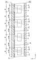
- an opening 28 a is partially formed in the first reflection sheet 28 disposed in the first light source sandwiching portion 27 c of the frame 27, and this opening A part of the first light source sandwiching portion 27c is exposed to the back side, that is, the LED 24 side through 28a. Since the light source reflectance of the first light source sandwiching portion 27c is relatively lower than that of the first reflection sheet 28, the LED 24 passes through the opening 28a in the surface facing the LED 24 in the first light source sandwiching portion 27c. The portion exposed to the side is the low light reflectance portion 31. That is, the formation range of the opening 28 a in the first reflection sheet 28 coincides with the formation range of the low light reflectance portion 31.
- the low light reflectivity portion 31 is constituted by a part of the frame 27, and the surface color is black, so that the light reflectivity is 0% as shown in FIG. It is a close value (for example, a range of 0% to 10%).
- the portion of the first reflective sheet 28 that remains without being formed with the opening 28a has a relatively higher light reflectance than the first light source sandwiching portion 27c exposed through the opening 28a.
- a high light reflectance portion 32 is configured. Since the high light reflectance portion 32 is configured by the first reflection sheet 28 having a white surface, the light reflectance is a value close to 100% (for example, a range of 90% to 100%), In FIG. 12, ⁇ % is set.
- a plurality of openings 28 a are intermittently arranged in parallel along the extending direction (X-axis direction) in the first reflecting sheet 28, and the arrangement interval is the LED 24. It is assumed that it is associated with the array interval. That is, the plurality of openings 28 a are formed in the first reflective sheet 28 so that the arrangement in the X-axis direction (the LED 24 arrangement direction) matches the arrangement in the X-axis direction of the plurality of LEDs 24. Accordingly, the opening 28a is in a positional relationship overlapping with a part of the light source arrangement area LA on the surface of the first light source sandwiching section 27c facing the LED 24 in the X-axis direction, whereby the low light reflectance part 31 is in the light source arrangement area.
- the non-formation portion of the opening 28a in the first reflection sheet 28 is in a positional relationship overlapping with the light source non-arrangement region LN on the surface facing the LED 24 of the first light source sandwiching portion 27c in the X-axis direction, thereby high light reflection.
- the rate part 32 is arranged in the light source non-arrangement region LN.
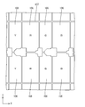
- the low light reflectance portion 31 and the high light reflectance portion 32 are arranged alternately in parallel along the X-axis direction on the surface of the first light source sandwiching portion 27c facing the LED 24, and when viewed in a plane, As shown in FIG.
- the black portions that are the low light reflectance portions 31 and the white portions that are the high light reflectance portions 32 are alternately and repeatedly arranged in the X-axis direction to form black and white stripes.
- the number of openings 28a in the first reflection sheet 28 matches the number of LEDs 24 in parallel, as shown in FIGS.
- the opening 28 a (low light reflectance portion 31) is concentric with the center position in the X-axis direction coinciding with the center position in the LED 24 (light source arrangement area LA).
- the dimension W1 in the X-axis direction in the opening 28a (low light reflectance part 31) is relatively smaller than the same dimension W2 in the LED 24 (light source arrangement area LA). That is, the low light reflectance portion 31 is formed narrower in the X-axis direction than the light source arrangement area LA, and is disposed in the center portion of the light source arrangement area LA in the X-axis direction. It can be said that it is not arranged at both ends.
- the high light reflectance portion 32 constituted by the first reflection sheet 28 is concentric with the central position in the X-axis direction being coincident with the central position in the light source non-arrangement region LN.
- the dimension (interval between adjacent openings 28a) W3 in the X-axis direction of the high light reflectance portion 32 is relatively larger than the same dimension W4 in the light source non-arrangement region LN. That is, the high light reflectance portion 32 is formed wider in the X-axis direction than the light source non-arrangement region LN, and in addition to the entire area of the light source non-arrangement region LN, in the X-axis direction in the adjacent light source arrangement region LA.
- the high light reflectance part 32 is further extended from the light source non-arrangement area LN to the light source arrangement area LA and is arranged over a part of the light source arrangement area LA.
- the low light reflectivity part 31 and the high light reflectivity part 32 are symmetrical with respect to the X-axis direction. Accordingly, the high light reflectance portion 32 positioned between the adjacent LEDs 24 (light source arrangement areas LA) is arranged in the light source arrangement in the pair of light source non-arrangement areas LN adjacent to both sides in the X-axis direction with respect to the light source arrangement area LA.
- the arrangement is such that the same dimension overlaps each end on the region LA side. Further, as shown in FIGS.
- the opening 28 a and the low light reflectivity portion 31 have dimensions in the Y-axis direction, that is, the alignment direction of the LED 24 and the light incident surface 26 b of the LED 24 on the LED substrate 25.
- the distance between the mounting surface and the light incident surface 26b of the light guide plate 26 is substantially equal.
- each LED 24 When each LED 24 is turned on, the light emitted from each LED 24 enters the light incident surface 26b of the light guide member 26 as shown in FIG. Although a predetermined space is held between the LED 24 and the light incident surface 26b, the space is sandwiched between the first reflective sheet 28 on the front side and the second reflective sheet 29 on the back side. Accordingly, the light from the LED 24 is repeatedly reflected between the reflecting sheets 28 and 29, and thus efficiently enters the light incident surface 26b.
- the light incident on the light incident surface 26 b is reflected by the light guide reflection sheet 30, propagates through the light guide member 26, is emitted from the light exit surface 26 a, and then passes through each optical member 23.
- the liquid crystal panel 11 is reached.
- the light amount incident on the light incident surface 26b of the light guide plate 26 may be uneven depending on the arrangement pattern and the non-arrangement pattern in the plurality of LEDs 24 arranged intermittently. That is, a relatively large amount of light emitted from the LED 24 is incident on a portion of the light incident surface 26b that directly faces the LED 24, in other words, the light source arrangement region LA that overlaps the LED 24 with respect to the arrangement direction of the LEDs 24. Is relatively lightly incident on a portion that does not directly face, in other words, in the light source non-arrangement region LN that does not overlap the LED 24 in the arrangement direction of the LEDs 24 (see FIG. 6).
- unevenness occurs in the amount of light incident on the light incident surface 26b, which may cause uneven brightness in the emitted light emitted from the light exit surface 26a.
- the interval between the LED 24 and the light incident surface 26b is narrowed in order to narrow the frame of the liquid crystal display device 10 and the backlight device 12, the light from the LED 24 directly enters the light incident surface 26b. Since the light is incident, the above-described unevenness tends to become more prominent.
- narrowing the frame means to narrow the width of the frame portion which is a non-light emitting portion in the liquid crystal display device 10 and the backlight device 12, and this frame portion includes the LED 24, the LED substrate 25, And since the edge part which has the light-incidence surface 26b in the light-guide plate 26 is distribute
- the light reflectance is relative to the surface facing the LED 24 in the first light source sandwiching portion 27 c among the pair of light source sandwiching portions 22 c and 27 c sandwiching the LED 24.
- the low light reflectance portion 31 that is low is arranged following the light source placement region LA that is the placement pattern of the LED 24, whereas the high light reflectance portion 32 that has a relatively high light reflectance is the non-placement pattern of the LED 24. It is arranged following a certain light source non-arrangement region LN.
- the first reflection sheet 28 attached to the surface of the first light source sandwiching portion 27c facing the LED 24 is formed with an opening 28a that overlaps a part of the light source arrangement area LA.
- the low light reflectance portion 31 is formed by the portion exposed to the LED 24 through the opening 28a in the one light source sandwiching portion 27c, whereas the high light reflectance portion 32 is formed by the first reflection sheet 28 in which the opening 28a is not formed. It is configured. In such a configuration, reflection of light, which tends to be excessive, is suppressed by the low light reflectance portion 31 arranged following the light source arrangement area LA until the light from the LED 24 enters the light incident surface 26b. In contrast, the high light reflectance portion 32 arranged following the light source non-arrangement region LN can improve the efficiency of light reflection that tends to be insufficient.
- the amount of light incident on the light incident surface 26b of the light guide plate 26 is made uniform regardless of the light source arrangement area LA and the light source non-arrangement area LN in the plurality of LEDs 24 that are intermittently arranged side by side. Become.
- the high light reflectance portion 32 is disposed on the surface facing the LED 24 in the first light source sandwiching portion 27c over the entire area of the light source non-arrangement region LN and further to the end of the adjacent light source arrangement region LA. Therefore, the reflection of light that tends to be insufficient in the entire area of the light source non-arrangement region LN can be further improved by the high light reflectance portion 32, and the light amount is relatively higher in the light source arrangement region LA than in the central portion side. Even at the end portion that tends to be insufficient, light can be efficiently reflected by the high light reflectance portion 32, so that the amount of incident light on the light incident surface 26b is less likely to be uneven.
- the formation range of the high light reflectance portion 32 is extended until it overlaps the end portion of the light source arrangement region LA, whereby the overall light utilization efficiency and the luminance of the emitted light can be further increased. Furthermore, since the low light reflectivity part 31 is arranged at the central part in the light source arrangement area LA on the surface facing the LED 24 in the first light source sandwiching part 27c, the light source arrangement area LA that tends to have an excessive amount of light. The reflection of light at the center of the light can be suppressed, and the luminance unevenness can be more effectively suppressed.
- the low light reflectance portion 31 and the high light reflectance portion 32 are disposed on the first light source sandwiching portion 27 c disposed on the front side of the LED 24, that is, on the light emitting surface 26 a side of the light guide plate 26.
- the light reflected by the low light reflectance portion 31 and the high light reflectance portion 32 is directed to the back side, that is, the side opposite to the light emitting surface 26a side, and then on the surface facing the LED 24 in the second light source sandwiching portion 22c. Or is incident on the light incident surface 26b and travels toward the surface 26c of the light guide plate 26 opposite to the light exit surface 26a side.
- the light reflected by the low light reflectance portion 31 and the high light reflectance portion 32 enters the light incident surface 26b and exits from the light exit surface 26a as it is.
- unevenness in luminance is less likely to occur in the outgoing light from the light outgoing surface 26a of the light guide plate 26.
- it is useful for narrowing the frame of the liquid crystal display device 10 and the backlight device 12.
- the backlight device (illumination device) 12 includes a plurality of LEDs (light sources) 24 arranged intermittently side by side, and a surface parallel to the direction in which the LEDs 24 are arranged, and the LED 24.
- a light guide plate 26 having a light incident surface 26b on which light from the LED 24 is incident and a light exit surface 26a for emitting the incident light, and the light of the light guide plate 26, which are arranged to face each other with an interval therebetween.
- the LED 24 is disposed on a surface facing the LED 24 in at least one of the pair of light source sandwiching portions 22c and 27c and the pair of light source sandwiching portions 22c and 27c that are disposed so as to sandwich the LED 24 from the emission side and the opposite side.
- the light emitted from the plurality of LEDs 24 is incident on the light incident surface 26b arranged in parallel with the LED 24 and facing the LEDs 24, and then propagates through the light guide plate 26. Is emitted from the light exit surface 26a.
- the amount of light incident on the light incident surface 26b of the light guide plate 26 may be uneven depending on the arrangement pattern and the non-arrangement pattern in the plurality of LEDs 24 that are intermittently arranged, and in particular, the backlight device.
- the distance between the LED 24 and the light incident surface 26b is narrowed in order to narrow the frame at 12, the occurrence of unevenness tends to become more prominent.
- the low light reflectance portion 31 having a relatively low light reflectance follows the arrangement pattern of the LEDs 24 on the surface facing the LED 24 in at least one of the pair of light source sandwiching portions 22c and 27c.
- the high light reflectance portion 32 having a relatively high light reflectance is arranged following the non-arrangement pattern of the LED 24, so that the light from the LED 24 is incident on the light incident surface 26b.
- reflection of light that tends to be excessive can be suppressed by the low light reflectance portion 31 that follows the arrangement pattern of the LED 24, whereas it is insufficient by the high light reflectance portion 32 that follows the non-arrangement pattern of the LED 24. It is possible to increase the efficiency of light reflection.
- the amount of light incident on the light incident surface 26b of the light guide plate 26 is made uniform regardless of the arrangement pattern and the non-arrangement pattern in the plurality of LEDs 24 that are intermittently arranged side by side, and unevenness hardly occurs. Thereby, luminance unevenness is less likely to occur in the outgoing light from the light outgoing surface 26a of the light guide plate 26.
- the backlight device 12 is useful for narrowing the frame.
- the high light reflectance portion 32 is arranged over the entire area of the non-arranged pattern of the LEDs 24 on the surface facing the LED 24 in at least one of the pair of light source sandwiching portions 22c and 27c. In this way, it is possible to further increase the efficiency of light reflection which tends to be insufficient by the high light reflectance portion 32 disposed over the entire area of the non-arrangement pattern of the LED 24. Thereby, luminance unevenness can be more effectively suppressed, and the overall light utilization efficiency and the luminance of the emitted light can be increased.
- the high light reflectance portion 32 is arranged in a range from the non-arrangement pattern of the LED 24 to the end portion of the arrangement pattern of the LED 24 on the surface facing the LED 24 in at least one of the pair of light source sandwiching portions 22c and 27c. Yes. If it does in this way, in the surface facing LED24 in at least any one of a pair of light source clamping parts 22c and 27c, the low light reflectance part 31 will be distribute
- the light amount from the LED 24 is relatively greater at the end portion of the arrangement pattern of the LED 24 than at the central portion of the arrangement pattern of the LED 24. Therefore, the light is efficiently reflected by the high light reflectance portion 32 at the end portion, which is suitable for further suppression of luminance unevenness.
- the low light reflectance portion 31 is disposed at least in the central portion of the arrangement pattern of the LEDs 24 on the surface facing the LEDs 24 in at least one of the pair of light source sandwiching portions 22c and 27c. If it does in this way, compared with the edge part of the arrangement pattern of LED24 in the center part of the arrangement pattern of LED24 in the surface facing LED24 in at least any one of a pair of light source clamping parts 22c and 27c, it is from LED24. Since the amount of light is relatively large, luminance unevenness can be more effectively suppressed by suppressing light reflection by the low light reflectance portion 31 at the central portion.
- the low light reflectivity part 31 and the high light reflectivity part 32 are alternately arranged in the arrangement direction of the LEDs 24 on the surface facing the LED 24 in one of the pair of light source sandwiching parts 22c and 27c. .
- the amount of light incident on the light incident surface 26b is uniform by the low light reflectance portion 31 and the high light reflectance portion 32 disposed on the surface facing the LED 24 in one of the pair of light source sandwiching portions 22c and 27c.
- the low light reflectivity part and the high light reflectivity part are arranged in both of the pair of light source sandwiching parts 22c and 27c, it is possible to cope with the low cost and the light by the low light reflectivity part 31. It is possible to prevent excessive reflection suppression.
- the low light reflectance portion 31 and the high light reflectance portion 32 are disposed on the light source sandwiching portions 22c and 27c that are disposed on the light emitting side with respect to the LED 24.
- the light reflected by the low light reflectance portion 31 and the high light reflectance portion 32 in the light source sandwiching portions 22c and 27c disposed on the light emitting side with respect to the LED 24 is opposite to the light emitting side.
- the light source sandwiching portions 22c and 27c disposed on the side opposite to the light emitting side the light is reflected by the surface facing the LED 24, or is incident on the light incident surface 26b and is emitted from the light guide plate 26. It will go to the opposite side of the side.
- the reflected light from the low light reflectance portion 31 and the high light reflectance portion 32 enters the light incident surface 26b and exits from the light exit surface 26a as it is, so that uneven brightness is less likely to occur in the emitted light. Become.
- one of the pair of light source sandwiching portions 22c and 27c is a frame (pressing member) 27 that presses the light guide plate 26 from the light emitting side.
- the frame 27 is assembled, the light guide plate 26 can be pressed from the light emitting side, and the light source sandwiching portions 22c and 27c of the frame 27 can be appropriately positioned with respect to the LED 24 and the light guide plate 26. Can be arranged. Thereby, it is excellent in assembly workability.
- one of the pair of light source sandwiching portions 22c and 27c is a chassis 22 that houses the LED 24 and the light guide plate 26.
- the LED 24 and the light guide plate 26 are arranged at appropriate positions with respect to the light source sandwiching portions 22 c and 27 c of the chassis 22. Thereby, it is excellent in assembly workability.
- the pair of light source sandwiching portions 22c and 27c are provided with reflection sheets (reflective members) 28 and 29 along the direction in which the LEDs 24 are arranged, and at least one of the pair of light source sandwiching portions 22c and 27c is a reflective member.
- a certain first reflection sheet 28 an opening 28 a that overlaps at least a part of the non-arranged pattern of the LED 24 is formed, and the low light reflectance portion 31 is configured by the light source sandwiching portions 22 c and 27 c exposed through the opening 28 a.
- the high light reflectance portion 32 is configured by the first reflection sheet 28.
- the low light reflectance portion 31 and the high light reflectance portion 32 are formed by forming the opening 28a in the first reflection sheet 28, so that the first reflection sheet is temporarily printed. Compared with the case where it corresponds by, it can respond at low cost.
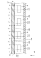
- a sheet 33 with a reflecting portion is attached to the surface of the first light source sandwiching portion 127 c of the frame 127 according to this embodiment that faces the LED 24.
- the reflection portion-attached sheet 33 is formed on the surface of a translucent base material (low-light-reflectance base material) 33a made of a substantially transparent synthetic resin material (for example, PET) and the translucent base material 33a, and light. It is comprised from the light reflection part (high light reflectance printing part) 33b which exhibits the white which was excellent in reflectivity. Since the translucent substrate 33a has a property of transmitting most of the irradiated light, its light reflectance is extremely low, which is a value close to 0%.
- the light reflecting portion 33b is formed by printing on the surface of the light transmissive substrate 33 a paste having a high light reflectance material, for example, a metal oxide, which has a higher light reflectance than the light transmissive substrate 33a.
- the light reflectance thereof is relatively higher than that of the translucent substrate 33a, for example, a value close to 100%, that is, the same as the light reflectance in each of the reflection sheets 28 to 30 described in the first embodiment. Value.
- the arrangement pattern of the light reflection part 33b in the translucent base material 33a overlaps with the non-arrangement pattern of the LED 24, that is, the light source non-arrangement region LN, on the surface facing the LED 24 in the first light source sandwiching part 127c. Yes.
- the light reflecting portion 33b constitutes a high light reflectance portion 132 having a relatively high light reflectance, whereas the light reflecting portion 33b of the translucent base material 33a is not printed. Constitutes a low light reflectance part 131 having a relatively low light reflectance.
- the light reflection part 33b since it is the same as that of the high light reflectivity part 32 (non-formation part of the opening part 28a in the 1st reflection sheet 28) described in Embodiment 1 mentioned above, it overlaps with description. Will be omitted.
- the pair of light source sandwiching portions 22c and 127c is provided with the reflection portion-attached sheet 33 and the second reflection sheet 29 (reflection member) along the direction in which the LEDs 24 are arranged.
- the light-source sandwiching portions 22c and 127c which are at least one of the reflecting members, has a reflection portion-attached sheet 33 having a translucent base material (low light reflectance base material) 33a having a relatively low light reflectance, A light reflecting portion (high light reflectance printing portion) 33b formed by printing a high light reflectance material having a relatively high light reflectance on a portion of the translucent base material 33a that overlaps at least a part of the arrangement pattern of the LEDs 24.
- the high light reflectance portion 132 is configured by the light reflecting portion 33b, whereas the non-printing portion 33a1 in which the light reflecting portion 33b is not printed out of the translucent base material 33a.
- Light reflectance portion 31 is formed.
- the low light reflectance part 31 and the high light reflectance part 32 are configured by printing the high light reflectance material on the translucent base material 33a to form the light reflecting part 33b.
- the mechanical strength of the reflection portion-attached sheet 33 can be maintained high.
- Embodiment 3 of the present invention will be described with reference to FIG.
- this Embodiment 3 what changed the structure of the 1st reflective sheet 128 from above-mentioned Embodiment 1 is shown.
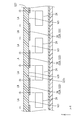
- the first reflective sheet 228 is formed on the surface of the reflective sheet base material 34 that has a light-reflecting white surface and is reflected on the surface of the reflective sheet base material 34. It comprises a light absorption part (low light reflectance printing part) 35 having a light reflectance that is relatively lower than that of the sheet substrate 34.
- the light absorbing portion 35 is formed by printing on the surface of the reflective sheet base material 34 a paste containing a low light reflectance material, for example, a black pigment, whose light reflectance is lower than that of the material forming the reflective sheet base material 34. Has been.
- the light absorbing portion 35 since the light absorbing portion 35 has a black surface and absorbs most of the irradiated light, its light reflectance is extremely low, for example, a value close to 0%. The value is sufficiently lower than that of the reflective sheet base material 34. And the arrangement pattern of the light absorption part 35 in the reflective sheet base material 34 overlaps with the arrangement pattern of the LED 24, that is, the light source arrangement area LA, on the surface of the first light source sandwiching part 227c facing the LED 24. Accordingly, the light absorbing portion 35 constitutes the low light reflectance portion 231 having a relatively low light reflectance, whereas the non-printing portion 34a in which the light absorbing portion 35 is not printed in the reflective sheet base material 34.
- each of the pair of light source sandwiching portions 22c and 227c is provided with the reflection sheets 29 and 228 along the alignment direction of the LEDs 24, and at least of the pair of light source sandwiching portions 22c and 227c.
- the first reflection sheet 228 that is either one of the reflection members has a reflection sheet base material (high light reflectance base material) 34 having a relatively high light reflectance, and the LED 24 is not disposed in the reflection sheet base material 34.
- the light absorbing portion (low light reflectance printing portion) 35 is formed by printing a low light reflectance material having a relatively low light reflectance on a portion that overlaps at least a part of the pattern.
- the low light reflectance portion 231 is configured by 35, whereas the high light reflectance portion 232 is configured by the non-printing portion 34a in which the light absorbing portion 35 is not printed in the reflective sheet base material 34. That.
- the low light reflectance portion 231 and the high light reflectance portion 232 are configured by printing the low light reflectance material on the reflective sheet base material 34 to form the light absorbing portion 35.
- the mechanical strength of the first reflection sheet 228 can be maintained high.
- Embodiment 4 A fourth embodiment of the present invention will be described with reference to FIG. In this Embodiment 4, what changed the formation range of the opening part 328a in the 1st reflective sheet 328 from above-mentioned Embodiment 1 is shown. In addition, the overlapping description about the same structure, an effect
- the first reflective sheet 328 As shown in FIG. 15, an opening 328a whose dimension in the X-axis direction is larger than that of the opening 28a described in the first embodiment is formed.
- the dimension W5 in the X-axis direction in the opening 328a and the low light reflectivity part 321, that is, the dimension in which the LEDs 24 are arranged is the same as the dimension W2 in the X-axis direction in the LED 24 and the light source arrangement area LA. .
- the dimension W6 in the X-axis direction in the high light reflectance portion 322 is the same as the dimension W4 in the X-axis direction in the light source non-arrangement region LN.
- the low light reflectance portion 321 is disposed over the entire light source arrangement region LA
- the high light reflectance portion 322 is disposed over the entire light source non-arrangement region LN.
- a fifth embodiment of the present invention will be described with reference to FIG.
- a configuration in which the formation range of the opening 428a in the first reflection sheet 428 is further changed from the above-described fourth embodiment is shown.
- the first reflective sheet 428 is formed with an opening 428 a whose dimension in the X-axis direction is further enlarged than the opening 328 a described in the fourth embodiment. .
- the dimension W7 in the X-axis direction in the opening 428a and the low light reflectivity part 421, that is, the alignment direction of the LEDs 24, is larger than the dimension W2 in the X-axis direction in the LED 24 and the light source arrangement area LA.
- the dimension W8 in the X-axis direction in the high light reflectance portion 422 is set to be smaller than the dimension W4 in the X-axis direction in the light source non-arrangement region LN.
- the low light reflectance portion 421 is arranged over the entire light source arrangement region LA, while the high light reflectance portion 422 is a part of the light source non-arrangement region LN (the alignment direction of the LEDs 24). It is arranged so as to overlap only with respect to the central part.
- Embodiment 6 of the present invention will be described with reference to FIG.
- the first reflective sheet 528 is changed from the first embodiment.
- the first reflection sheet 528 includes a plurality of divided reflection sheets 36 divided for each light source non-arrangement region LN.
- Each divided reflection sheet 36 is attached to a position overlapping with each light source non-arrangement region LN on the surface of the frame 527 facing the LED 24 in the first light source sandwiching portion 527c, and constitutes a high light reflectance portion 522. Therefore, the portion where the split reflection sheet 36 is not attached on the surface of the first light source sandwiching portion 527c of the frame 527 facing the LED 24 constitutes the low light reflectance portion 521.
- Embodiment 7 A seventh embodiment of the present invention will be described with reference to FIG. In this Embodiment 7, what changed the structure of the 1st reflective sheet from above-mentioned Embodiment 1 is shown. In addition, the overlapping description about the same structure, an effect
- the first reflective sheet according to the present embodiment has a configuration in which a high light reflectance part having a relatively higher light reflectance than the base material of the first reflective sheet is formed in a portion overlapping each light source arrangement region LA. . That is, when the light reflectance at the base material of the first reflective sheet is ⁇ % and the light reflectance at the high light reflectance portion is ⁇ %, the latter ( ⁇ %) is the former ( ⁇ %) as shown in FIG. ) Is a relatively high value, and is closer to 100%.
- a high light reflectance part can be formed by printing the high light reflectance material whose light reflectance is higher than a base material, for example on the surface of a 1st reflective sheet.
- a high light reflectivity portion is formed by attaching a high light reflectivity sheet made of a high light reflectivity material having a light reflectivity higher than that of the base material to the surface of the first reflection sheet. Is also possible.
- the present invention is not limited to the embodiments described with reference to the above description and drawings.
- the following embodiments are also included in the technical scope of the present invention.
- the arrangement order of the colored portions R, G, B, and Y in the color filter can be appropriately changed.
- the present invention includes an arrangement in which the colored portion B, the green colored portion G, the red colored portion R, and the yellow colored portion Y are arranged in this order along the X-axis direction.
- the colored portions R, G, B, and Y in the color filter are red colored portions R and green colored portions G from the left side of the drawing.
- the present invention also includes an arrangement in which the yellow colored portion Y and the blue colored portion B are arranged in this order along the X-axis direction.
- the colored portions R, G, B, and Y in the color filter are red colored portions R and yellow from the left side of the drawing.
- the present invention also includes an arrangement in which the colored portion Y, the green colored portion G, and the blue colored portion B are arranged in this order along the X-axis direction.
- the three primary colors of light, red (R), green (G), and blue (B) are added to yellow (Y) as the colored portion of the color filter.
- Y yellow
- a cyan colored portion C may be added instead of the yellow colored portion.
- the color filter has four colored portions.
- the transparent color does not color transmitted light at the yellow colored portion installation position.
- the portion T may be provided.
- the transparent portion T has substantially the same transmittance for all wavelengths at least in the visible light, so that the transmitted light is not colored into a specific color.
- the four colored portions R, G, B, and Y constituting the color filter are illustrated as being arranged in the row direction.
- the four colored portions R are arranged.
- G, B, and Y may be arranged in a matrix.
- the four colored portions R, G, B, and Y are arranged in a matrix with the X-axis direction as the row direction and the Y-axis direction as the column direction.
- the colored portions R, G, B, and Y arranged in adjacent rows are in the column direction (Y The dimensions in the axial direction are different from each other.
- the red colored portion R and the blue colored portion B are arranged adjacent to each other in the row direction, whereas the row having a relatively small size in the column direction.
- the green colored portion G and the yellow colored portion Y are arranged adjacent to each other in the row direction.
- the first colored row R and the blue colored portion B are alternately arranged in the row direction, the first row having a relatively large dimension in the column direction, the green colored portion G, and the yellow colored portion Y.
- the first row having a relatively large dimension in the column direction
- the green colored portion G and the yellow colored portion Y.
- the area of the red coloring part R and the blue coloring part B is made larger than the areas of the green coloring part G and the yellow coloring part Y.
- the green colored portion G is arranged adjacent to the red colored portion R in the column direction
- the yellow colored portion Y is arranged adjacent to the blue colored portion B in the column direction. Yes.
- the dimensions in the column direction of the pixel electrodes 115 arranged in adjacent rows are different as shown in FIG. That is, the area of each pixel electrode 115 that overlaps with the red colored portion R or the blue colored portion B is larger than the area of the pixel electrode 115 that overlaps with the yellow colored portion Y or the green colored portion G. .
- the film thicknesses of the colored portions R, G, B, and Y are all equal.
- the source wirings 117 are all arranged at an equal pitch, while the gate wirings 116 are arranged at two different pitches according to the dimensions of the pixel electrodes 115 in the column direction. 24 and 25 show a case where the areas of the red colored portion R and the blue colored portion B are about 1.6 times the areas of the yellow colored portion Y and the green colored portion G. Show.
- the yellow colored portion Y is arranged adjacent to the red colored portion R in the column direction with respect to the color filter. It is also possible to adopt a configuration in which the green colored portion G is arranged adjacent to the colored portion B in the column direction.
- the color portions R, G, B, and Y constituting the color filter are illustrated with different area ratios.
- the areas of the colored portions R, G, B, and Y are exemplified. It is also possible to adopt a configuration in which the ratio is made equal.
- the colored portions R, G, B, and Y are arranged in a matrix with the X-axis direction as the row direction and the Y-axis direction as the column direction.
- the dimensions in the row direction (X-axis direction) in R, G, B, and Y are all the same, and the dimensions in the column direction (Y-axis direction) are all the same.
- the areas of the colored portions R, G, B, and Y are all equal.
- the color filter is configured as described above, in the array substrate, as shown in FIG. 28, the dimension in the row direction of each pixel electrode 215 facing each colored portion R, G, B, Y is shown in FIG.
- the dimensions in the column direction are all equal, so that all the pixel electrodes 215 have the same shape and the same area.
- the gate wiring 216 and the source wiring 217 are all arranged at an equal pitch.
- the color filter has four colored portions. However, as shown in FIG. 29, the yellow colored portion is omitted, and red (R), which is the primary color of light. , Green (G), and blue (B) are also included in the present invention. In this case, it is preferable to make the area ratios of the colored portions R, G, and B equal.
- the structure related to the pixel has been described using the simplified drawings (FIGS. 4 and 5). However, in addition to the structure disclosed in these drawings, the specific structure related to the pixel is changed. Is possible.
- the present invention can also be applied to a structure in which one pixel is divided into a plurality of sub-pixels and the sub-pixels are driven so as to have different gradation values, so-called multi-pixel driving is performed.
- one pixel PX is composed of a pair of subpixels SPX
- the pair of subpixels SPX is composed of a pair of adjacent pixel electrodes with the gate wiring 102 interposed therebetween. 100.
- the TFT 101 includes a gate electrode 101a constituted by a part of the gate wiring 102, a source electrode 101b constituted by a pair of branch lines branched from the source wiring 103 and disposed on the gate electrode 101a, and the gate electrode 101a. And a drain electrode 101c arranged between the pair of source electrodes 101b, and arranged in the direction (Y-axis direction) of the pair of sub-pixels SPX forming one pixel PX on the gate wiring 102. A pair is lined up along.
- the drain electrode 101c of the TFT 101 is connected to the other end side of the drain wiring 104 having a contact portion 104a connected to the pixel electrode 100 on one end side.
- the contact portion 104a and the pixel electrode 100 are connected through a contact hole CH formed in an interlayer insulating film (not shown) interposed therebetween, and have the same potential.
- the auxiliary capacitance wiring 105 is arranged at the end opposite to the gate wiring 102 side so as to overlap each other in plan view, and the pixel on which the auxiliary capacitance wiring 105 overlaps. A capacitance is formed with the electrode 100.
- the pair of pixel electrodes 100 constituting one pixel PX forms a capacitance with different auxiliary capacitance lines 105.
- Each in-pixel auxiliary capacitance line 108 is connected to each auxiliary capacitance line 105 arranged on the side opposite to the gate line 101 side by a connection line 109, thereby having the same potential as each auxiliary capacitance line 105. ing.
- the in-pixel auxiliary capacitance line 108 having the same potential as that of the auxiliary capacitance line 105 is superimposed on the plane and forms a capacitance with each contact portion 104a having the same potential as each pixel electrode 100.
- the scanning signal and the data signal are supplied from the common gate wiring 102 and the source wiring 103 to the pair of TFTs 101, respectively, while the pair of pixel electrodes 100 and the pair of contact portions connected thereto.
- the voltage value charged to each sub-pixel SPX, that is, the gradation value is different from each other.
- so-called multi-pixel driving can be performed, and good viewing angle characteristics can be obtained.
- the coloring portions R, G, B, and Y of the color filter 106 that faces the pixel electrode 100 and the pixel electrode 100 are as follows. It is supposed to be configured. That is, as shown in FIG. 31, the color filter 106 is composed of four colored portions R, G, B, and Y. From the left side of the drawing, the yellow colored portion Y, the red colored portion R, and the green colored portion. G and blue colored portion B are repeatedly arranged in parallel along the X-axis direction in this order. Each of the colored portions R, G, B, and Y is partitioned by a light shielding layer (black matrix) 107.
- black matrix black matrix
- the light shielding layer 107 overlaps with the gate wiring 102, the source wiring 103, and the auxiliary capacitance wiring 105 in a plan view. Are arranged in a substantially lattice pattern.
- the yellow colored portion Y and the green colored portion G have substantially the same dimensions in the X-axis direction (the parallel direction of the colored portions R, G, B, and Y).
- the red colored portion R and the blue colored portion B are relatively larger in dimensions in the X-axis direction than the yellow colored portion Y and the green colored portion G (for example, 1.3 times to 1). About 4 times).
- the red colored portion R has a slightly larger dimension in the X-axis direction than the blue colored portion B.
- each pixel electrode 100 has substantially the same size in the Y-axis direction, but the size in the X-axis direction has the colored portions R, G, B of the color filter 106 facing each other. , Y corresponding to the size of Y.
- the low light reflectance portion and the high light reflectance portion are arranged in the first light source sandwiching portion on the light emitting surface side among the pair of light source sandwiching portions. You may make it arrange
- the low light reflectance portion and the high light reflectance portion are symmetrical with respect to the arrangement direction of the LEDs.
- the low light reflectance portion and the high light reflectance portion are the LEDs.
- the present invention also includes an asymmetric shape in the arrangement direction.
- the low light reflectance portion and the high light reflectance portion are shown to be associated with each of the light source arrangement regions and the light source non-arrangement regions.
- One or both of the light reflectance part and the high light reflectance part are arranged in association with only a part of each light source arrangement region and each light source non-arrangement region.
- a configuration in which the low light reflectance portion and the high light reflectance portion are arranged at unequal pitches in the LED arrangement direction can be employed.
- the low light reflectivity portions have the same dimension in the LED alignment direction, but the low light reflectivity portions have different dimensions in the LED alignment direction. are also included in the present invention. This configuration can be similarly applied to the high light reflectance portion.
- the low light reflectance portion and the high light reflectance portion are arranged in the first light source sandwiching portion on the light emitting surface side among the pair of light source sandwiching portions.
- Either one of the reflectance part and the high light reflectance part may be arranged separately in the first light source sandwiching part, and the other side may be separately disposed in the second light source sandwiching part opposite to the light emitting surface side. .
- Embodiment 2 the case where the light reflecting portion is formed by printing the high light reflectance material on the surface of the sheet with the reflecting portion is shown.
- the high light reflectance material is formed on the surface of the sheet with the reflecting portion. It is also possible to form a light reflection part (high light reflectance application part) by coating.
- the present invention includes other means using other forming means such as metal vapor deposition.
- the base material forming the sheet with the reflecting portion is a light-transmitting base material excellent in light transmittance is shown, but light absorption excellent in light absorption is shown. It is also possible to use a conductive substrate.
- a light absorptive base material the thing made from the synthetic resin whose surface exhibits black is preferable.
- Embodiment 3 described above the case where the light absorbing portion is formed by printing a low light reflectance material on the surface of the first reflective sheet has been shown. However, the low light reflectance on the surface of the first reflective sheet is shown. It is also possible to form a light absorption part (low light reflectance application part) by applying a material.
- the present invention includes other means using other forming means such as metal vapor deposition.
- the low light reflectance portion and the high light reflectance portion are configured by attaching the first reflection sheet or the sheet with the reflection portion to the first light source sandwiching portion.
- the printed or coated portion By directly printing or applying a high light reflectance material to the first light source sandwiching portion, it is also possible to make the printed or coated portion a high light reflectance portion and the non-printed portion or non-coated portion to be a low light reflectance portion. It is.
- the low light reflectance part and the high light reflectance are provided in the second light source sandwiching part (part of the chassis) on the side opposite to the light emitting surface side of the pair of light source sandwiching parts.
- the present invention can be similarly applied when forming the portion.
- the green phosphor that emits green light and the red phosphor that emits red light is used as the phosphor used in the LED is shown.
- yellow that emits yellow light is used.
- the fluorescent substance independently is also contained in this invention.
- the yellow phosphor for example, ⁇ -SiAlON, which is a kind of SiAlON phosphor, is preferably used.
- the specific substance names of the phosphors of the respective colors can be appropriately changed other than those already described.
- an LED chip that emits blue light in a single color and a type of LED that emits substantially white light using a phosphor is used.
- the present invention includes an LED chip that incorporates an LED chip that emits ultraviolet light and that emits substantially white light using a phosphor.
- the phosphor it is preferable to use three colors: a blue phosphor that emits blue light, a green phosphor that emits green light, and a red phosphor that emits red light. The color of the phosphor can be changed as appropriate.
- an LED chip that emits blue light in a single color and a LED that emits substantially white light using a phosphor is used.
- red light, green light, and blue light are used.
- the present invention also includes an LED using a type of LED that incorporates three types of LED chips each emitting light in a single color.
- the present invention includes an LED using a type of LED in which three types of LED chips each emitting C (cyan), M (magenta), and Y (yellow) are monochromatic. In this case, the chromaticity of the LED can be adjusted by appropriately controlling the amount of current to each LED chip during lighting.
- the LED is used as the light source, but other light sources such as an organic EL can be used.
- a TFT is used as a switching element of a liquid crystal display device.
- the present invention can also be applied to a liquid crystal display device using a switching element other than TFT (for example, a thin film diode (TFD)).
- a switching element other than TFT for example, a thin film diode (TFD)
- the present invention can also be applied to a liquid crystal display device for monochrome display.
- liquid crystal display device using the liquid crystal panel as the display panel has been exemplified, but the present invention can also be applied to a display device using another type of display panel.
- the television receiver provided with the tuner is exemplified, but the present invention is also applicable to a display device that does not include the tuner.
- the light guide plate has a flat plate shape, and the light output surface and the opposite surface (surface facing the chassis) are used in parallel.
- the light guide plate having a wedge shape in cross section and the light emitting surface and the opposite surface are not included in the present invention.
- the light exit surface of the light guide plate is parallel to the bottom plate of the chassis, whereas the surface opposite to the light exit surface of the light guide plate is inclined with respect to the bottom plate and the light exit surface. can do.
- the surface opposite to the light exit surface of the light guide plate is parallel to the bottom plate of the chassis, whereas the light exit surface of the light guide plate is opposite to the surface opposite to the bottom plate and the light exit surface. It is possible to adopt an inclined shape.
- a pair of LED substrates are arranged at the ends of both long sides of the light guide plate.
- the LED substrates are both short sides of the light guide plate. What is arranged in a pair at the end of the side is also included in the present invention.
- the present invention includes one in which only one end of one long side or one short side of the light guide plate is disposed.
- a light guide plate having a wedge-shaped cross section as described in (30) above is used. Is possible.
- SYMBOLS 10 Liquid crystal display device (display device), 11 ... Liquid crystal panel (display panel), 12 ... Backlight device (illumination device), 22 ... Chassis, 22c ... 1st light source clamping part (Light source sandwiching part), 24 ... LED (light source), 26 ... light guide plate, 26a ... light emitting surface, 26b ... light incident surface, 27, 127, 227, 527 ... frame ( Pressing member), 27c, 127c, 227c, 527c ... second light source sandwiching portion (light source sandwiching portion), 28, 228, 328, 428, 528 ... first reflecting sheet (reflecting member), 28a, 328a, 428a ...
Landscapes
- Physics & Mathematics (AREA)
- General Physics & Mathematics (AREA)
- Optics & Photonics (AREA)
- Planar Illumination Modules (AREA)
Abstract
Le dispositif de rétroéclairage (12) de l'invention est équipé : d'une pluralité de DEL (24) placées en rang discontinu; d'une plaque de guidage de lumière (26) qui constitue une face parallèle à la direction de rangement des DEL (24), qui est placée en opposition et de manière à maintenir un espace entre les DEL (24), et qui possède une face incidence de lumière (26b) sur laquelle une lumière provenant des DEL (24) est incidente, et une face émission de lumière (26a) qui émet une lumière incidente; d'une paire d'unités d'enserrement de source lumineuse (22c, 27c) qui est placée de manière à enserrer la DEL (24) depuis le côté face émission de lumière (26a) de la plaque de guidage de lumière (26) et depuis le côté opposé à ce côté face émission de lumière (26a); d'une unité à faible taux de réflexion de lumière (31) qui est placée suivant un motif d'arrangement des DEL (24) sur une face opposée aux DEL (24) au niveau d'au moins l'une des deux unités d'enserrement de source lumineuse (22c, 27c) de la paire, et qui présente un taux de réflexion de lumière relativement faible; et d'une unité à taux élevé de réflexion de lumière (32) qui est placée suivant un motif de non-arrangement des DEL (24) sur une face opposée aux DEL (24) au niveau d'au moins l'une des deux unités d'enserrement de source lumineuse (22c, 27c) de la paire, et qui présente un taux de réflexion de lumière relativement élevé.
Applications Claiming Priority (2)
| Application Number | Priority Date | Filing Date | Title |
|---|---|---|---|
| JP2011120872 | 2011-05-30 | ||
| JP2011-120872 | 2011-05-30 |
Publications (1)
| Publication Number | Publication Date |
|---|---|
| WO2012165251A1 true WO2012165251A1 (fr) | 2012-12-06 |
Family
ID=47259110
Family Applications (1)
| Application Number | Title | Priority Date | Filing Date |
|---|---|---|---|
| PCT/JP2012/063157 Ceased WO2012165251A1 (fr) | 2011-05-30 | 2012-05-23 | Dispositif d'éclairage, dispositif d'affichage, et dispositif de réception de télévision |
Country Status (1)
| Country | Link |
|---|---|
| WO (1) | WO2012165251A1 (fr) |
Citations (4)
| Publication number | Priority date | Publication date | Assignee | Title |
|---|---|---|---|---|
| JP2003331628A (ja) * | 2002-03-05 | 2003-11-21 | Seiko Epson Corp | 照明装置、液晶装置及び電子機器 |
| WO2007032116A1 (fr) * | 2005-09-14 | 2007-03-22 | Sharp Kabushiki Kaisha | Dispositif d'affichage à cristaux liquides |
| JP2007294372A (ja) * | 2006-03-28 | 2007-11-08 | Harison Toshiba Lighting Corp | 面光源装置及び表示装置 |
| JP2009170386A (ja) * | 2008-01-21 | 2009-07-30 | Fujikura Ltd | 面状発光装置 |
-
2012
- 2012-05-23 WO PCT/JP2012/063157 patent/WO2012165251A1/fr not_active Ceased
Patent Citations (4)
| Publication number | Priority date | Publication date | Assignee | Title |
|---|---|---|---|---|
| JP2003331628A (ja) * | 2002-03-05 | 2003-11-21 | Seiko Epson Corp | 照明装置、液晶装置及び電子機器 |
| WO2007032116A1 (fr) * | 2005-09-14 | 2007-03-22 | Sharp Kabushiki Kaisha | Dispositif d'affichage à cristaux liquides |
| JP2007294372A (ja) * | 2006-03-28 | 2007-11-08 | Harison Toshiba Lighting Corp | 面光源装置及び表示装置 |
| JP2009170386A (ja) * | 2008-01-21 | 2009-07-30 | Fujikura Ltd | 面状発光装置 |
Similar Documents
| Publication | Publication Date | Title |
|---|---|---|
| KR101280390B1 (ko) | 엘이디 백라이트 유닛 및 이를 이용한 액정표시장치모듈 | |
| JP5416270B2 (ja) | 表示装置及びテレビ受信装置 | |
| US8939597B2 (en) | Illumination device, display device, and television reception device | |
| US9016923B2 (en) | Lighting device, display device, and television receiver | |
| WO2014087875A1 (fr) | Dispositif d'affichage et dispositif de réception de télévision | |
| WO2014141879A1 (fr) | Dispositif d'affichage et dispositif de réception de télévision | |
| US9164226B2 (en) | Illumination device, display device, and television reception device | |
| US20150168774A1 (en) | Display device and television receiver | |
| CN103392092B (zh) | 照明装置、显示装置、电视接收装置 | |
| US20140009695A1 (en) | Illumination device, display device, and television reception device | |
| US8944623B2 (en) | Display device and television receiver | |
| US9476577B2 (en) | Lighting device, display device, and television reception device | |
| WO2011074352A1 (fr) | Dispositif d'affichage et récepteur de télévision | |
| WO2013024715A1 (fr) | Dispositif d'éclairage, dispositif d'affichage, dispositif de réception de télévision | |
| KR101946263B1 (ko) | 액정표시장치 | |
| WO2012128076A1 (fr) | Dispositif d'éclairage, écran et dispositif de récepteur de télévision | |
| WO2025065380A1 (fr) | Structure de rétroéclairage, module d'affichage, écran en mosaïque et appareil d'affichage | |
| WO2012128063A1 (fr) | Dispositif d'éclairage, écran et dispositif de récepteur de télévision | |
| WO2012133036A1 (fr) | Dispositif d'éclairage, dispositif d'affichage, et dispositif de réception de télévision | |
| WO2011074353A1 (fr) | Dispositif d'affichage et récepteur de télévision | |
| KR101684611B1 (ko) | 액정표시장치 | |
| WO2012165249A1 (fr) | Dispositif d'éclairage, dispositif d'affichage et dispositif de réception de télévision | |
| WO2012165247A1 (fr) | Dispositif d'éclairage, dispositif d'affichage, et dispositif de réception de télévision | |
| WO2012165251A1 (fr) | Dispositif d'éclairage, dispositif d'affichage, et dispositif de réception de télévision | |
| KR101744873B1 (ko) | 액정표시장치 |
Legal Events
| Date | Code | Title | Description |
|---|---|---|---|
| 121 | Ep: the epo has been informed by wipo that ep was designated in this application |
Ref document number: 12793778 Country of ref document: EP Kind code of ref document: A1 |
|
| NENP | Non-entry into the national phase |
Ref country code: DE |
|
| 122 | Ep: pct application non-entry in european phase |
Ref document number: 12793778 Country of ref document: EP Kind code of ref document: A1 |
|
| NENP | Non-entry into the national phase |
Ref country code: JP |