WO2012168973A1 - 有機el素子及び有機el素子の製造方法 - Google Patents
有機el素子及び有機el素子の製造方法 Download PDFInfo
- Publication number
- WO2012168973A1 WO2012168973A1 PCT/JP2011/003240 JP2011003240W WO2012168973A1 WO 2012168973 A1 WO2012168973 A1 WO 2012168973A1 JP 2011003240 W JP2011003240 W JP 2011003240W WO 2012168973 A1 WO2012168973 A1 WO 2012168973A1
- Authority
- WO
- WIPO (PCT)
- Prior art keywords
- irradiation
- laser
- organic
- light emitting
- emitting region
- Prior art date
- Legal status (The legal status is an assumption and is not a legal conclusion. Google has not performed a legal analysis and makes no representation as to the accuracy of the status listed.)
- Ceased
Links
Images




Classifications
-
- H—ELECTRICITY
- H10—SEMICONDUCTOR DEVICES; ELECTRIC SOLID-STATE DEVICES NOT OTHERWISE PROVIDED FOR
- H10K—ORGANIC ELECTRIC SOLID-STATE DEVICES
- H10K71/00—Manufacture or treatment specially adapted for the organic devices covered by this subclass
-
- H—ELECTRICITY
- H10—SEMICONDUCTOR DEVICES; ELECTRIC SOLID-STATE DEVICES NOT OTHERWISE PROVIDED FOR
- H10K—ORGANIC ELECTRIC SOLID-STATE DEVICES
- H10K50/00—Organic light-emitting devices
- H10K50/80—Constructional details
-
- H—ELECTRICITY
- H10—SEMICONDUCTOR DEVICES; ELECTRIC SOLID-STATE DEVICES NOT OTHERWISE PROVIDED FOR
- H10K—ORGANIC ELECTRIC SOLID-STATE DEVICES
- H10K71/00—Manufacture or treatment specially adapted for the organic devices covered by this subclass
- H10K71/861—Repairing
Definitions
- the present invention relates to an organic EL device and a method for manufacturing an organic electroluminescence device.
- organic EL organic electroluminescence
- an organic layer is interposed between an anode (anode) and a cathode (cathode)
- conductive foreign matters are attached or mixed in the manufacturing process, or patterning is performed.
- an undesired short circuit occurs due to a defect in the organic EL element, and the organic EL element becomes defective.
- Patent Document 1 the depth of the electrode forming film removed by the laser irradiation is measured in the middle of the laser irradiation process, and the measured depth and the previously known electrode forming film before correction are measured.
- a technique for grasping the progress of correction at that time from the relationship with the thickness and adjusting the laser irradiation after the measurement is disclosed.
- Patent Document 2 the size of a foreign substance existing between the cathode and the anode and contributing to the short circuit between the cathode and the anode is measured, and the wavelength of the laser and the number of times of irradiation are set based on the size of the foreign substance.
- a method of irradiating a foreign substance with a set laser to remove at least a part of the foreign substance is disclosed.
- Patent Document 3 detects a potential defective portion of the organic EL element by fluorescence inspection by irradiation of the first ultraviolet laser, and irradiates the detected defective portion with the second repair ultraviolet laser, A method for removing a defective portion is disclosed.
- the depth of the electrode-forming film (irradiation mark) removed by laser irradiation is scattered by, for example, a surface roughness measuring device using a stylus method, a displacement meter using a laser measurement method, and laser irradiation.
- a surface roughness measuring device using a stylus method e.g., a surface roughness measuring device using a stylus method
- a displacement meter using a laser measurement method e.g., a laser measurement method
- laser irradiation e.g., a laser irradiation trace.
- the main purpose is to appropriately reduce the range of the fluorescence inspection in order to minimize the deterioration of the light emitting function of the organic EL element due to the ultraviolet laser for inspection and to shorten the inspection time.
- it does not show how to control the irradiation condition of the ultraviolet laser for repair.
- the present invention provides a method for manufacturing an organic EL element capable of adaptively, quickly, and easily controlling a laser irradiation condition for repairing a defect caused by a short circuit of the organic EL element, and such a manufacturing method. It aims at providing the organic EL element manufactured by this.
- a method for manufacturing an organic EL element includes a first laser irradiation that irradiates a light emitting region having a defective portion of an organic EL element with laser light under a first irradiation condition.
- a state observing step of observing a state of an irradiation mark generated in the light emitting region by irradiation of laser light in the first laser irradiation step, the first irradiation condition and the state of the observed irradiation mark Based on the irradiation condition determining step for determining a second irradiation condition for eliminating the defect caused by the defective portion, and the light emitting region in the second irradiation condition determined in the irradiation condition determining step A second laser irradiation step of irradiating the laser beam.
- preliminary irradiation for determining conditions of laser irradiation (secondary laser irradiation) at the time of repair in the light emitting region of the defective pixel. Therefore, there is no concern that the properties of the laser irradiation object will be different, for example, when preliminary irradiation is performed outside the light emitting region, and the conditions of laser irradiation at the time of repair can be accurately determined. It can be performed reliably and stably.
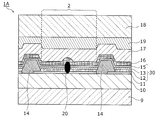
- FIG. 1 is a schematic cross-sectional view of an organic EL element according to an embodiment of the present invention.
- FIG. 2 is a top view of the organic EL element showing the state of the cathode having a high resistance.
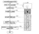
- FIG. 3 is a flowchart illustrating a method for manufacturing an organic EL element according to the present invention.
- FIG. 4 is a schematic cross-sectional view of the organic EL element prepared in the first step of the present invention.
- FIG. 5 is an operation flowchart for explaining step S20 according to the embodiment of the present invention.
- FIG. 6 is an operation flowchart for explaining step S30 according to the embodiment of the present invention.
- FIG. 7 is a system configuration diagram for carrying out laser repair according to the embodiment of the present invention.
- FIG. 1 is a schematic cross-sectional view of an organic EL element according to an embodiment of the present invention.
- FIG. 2 is a top view of the organic EL element showing the state of the cathode having a high resistance.
- FIG. 8 is a top view of an organic EL element showing a state of irradiation marks by laser irradiation.
- FIG. 9 is a diagram illustrating the light emission state of the pixel at the time of recovery lighting confirmation.
- FIG. 10 is an external view of a television system provided with the organic EL element of the present invention.
- the organic EL device manufacturing method includes a first laser irradiation step of irradiating a light emitting region having a defect portion of an organic EL device with laser light under a first irradiation condition, and the first laser.
- the irradiation condition determination step as the second irradiation condition, at least one of a focal depth, a pulse width, a frequency, and a power density of laser light may be determined.
- preliminary irradiation for determining the conditions of laser irradiation (secondary laser irradiation) at the time of repair is performed in the light emitting region of the defective pixel.
- primary laser irradiation for determining the conditions of laser irradiation (secondary laser irradiation) at the time of repair is performed in the light emitting region of the defective pixel.
- the defective portion may be a short-circuited portion between the anode and the cathode of the organic EL element.
- the laser beam is irradiated in a closed line shape surrounding the short-circuited portion of the light emitting region, whereby a resistance of a portion of the light emitting region located in the closed line shape is irradiated.
- the value may be higher than the resistance value before the laser light irradiation.
- the short-circuited portion is a light emitting region due to irradiation marks formed by laser irradiation at the time of repair.
- the light emitting function of the light emitting region can be recovered.
- the laser beam may be irradiated in a region that is to be surrounded by the closed line.
- the laser light irradiation in the first laser irradiation step and the laser light irradiation in the second laser irradiation step may be continuously performed using the same laser oscillator. .
- the organic EL device includes a light emitting region in which an anode, an organic light emitting layer, and a cathode are laminated in this order, a short-circuit portion between the anode and the cathode present in the light emitting region, and the light emission.
- the condition of the laser irradiation (second laser irradiation trace) at the time of repair is determined by performing preliminary irradiation (first laser irradiation trace) in the light emitting area of the defective pixel.
- preliminary irradiation first laser irradiation trace
- the conditions of laser irradiation at the time of repair can be determined accurately, so that repair is more reliable and stable.
- an organic EL device can be obtained.
- the first laser irradiation mark may be formed in a region surrounded by the second laser irradiation mark.
- the area of the light emitting region may be reduced due to laser irradiation marks at the time of preliminary irradiation. Absent.
- first laser irradiation trace and the second laser irradiation trace may be formed continuously.
- the resistance value of the portion of the light emitting region where the second laser irradiation trace is formed is such that neither the first laser irradiation trace nor the second laser irradiation trace of the light emitting region is formed. It is preferable that the resistance value is higher than that of the portion.
- the short-circuited portion is electrically separated from the light emitting region by the second laser irradiation trace, whereby an organic EL element in which the light emitting function of the light emitting region is restored can be obtained.
- FIG. 1 is a schematic cross-sectional view of an organic EL element 1 according to Embodiment 1 of the present invention.
- An organic EL device 1 shown in FIG. 1 is an organic functional device having an organic layer including an anode, a cathode, and a light emitting layer sandwiched between the two electrodes.
- the organic EL element 1 includes a planarizing film 10, an anode 11, a hole injection layer 12, a light emitting layer 13, a partition wall 14, and an electron injection layer 15 on a transparent glass 9. And a cathode 16, a thin film sealing layer 17, a sealing resin layer 19, and a transparent glass 18.
- the anode 11 and the cathode 16 correspond to the lower electrode layer and the upper electrode layer in the present invention, respectively.
- the hole injection layer 12, the light emitting layer 13, and the electron injection layer 15 correspond to the organic layers in the present invention.
- the transparent glasses 9 and 18 are substrates that protect the light emitting surface of the light emitting panel, and are, for example, transparent non-alkali glass having a thickness of 0.5 mm.
- the planarization film 10 is made of an insulating organic material, for example, and is formed on a substrate including, for example, a driving thin film transistor (TFT).
- TFT driving thin film transistor
- the anode 11 is an anode to which holes are supplied, that is, an electric current flows from an external circuit, and has a structure in which a reflective electrode made of, for example, Al or silver alloy APC is laminated on the planarizing film 10. Yes.
- the thickness of the reflective electrode is, for example, 10 to 40 nm.
- the anode 11 may have a two-layer structure made of, for example, ITO (Indium Tin Oxide) and silver alloy APC.
- the anode 11 is formed of a metal having a high reflectance such as APC, so that the irradiated laser light is reflected by the metal having a high reflectance. Therefore, the laser light is collected on a layer to be focused more efficiently. It becomes possible to shine.
- the hole injection layer 12 is a layer mainly composed of a hole injecting material.
- the hole injecting material is a material having a function of injecting holes injected from the anode 11 side into the light emitting layer 13 stably or by assisting the generation of holes.
- PEDOT polyethylene
- aniline aniline
- the light-emitting layer 13 is a layer that emits light when a voltage is applied between the anode 11 and the cathode 16, and includes, for example, a-NPD (Bis [N- (1-naphthyl) -N-phenyl] benzidine) as a lower layer, As an upper layer, Alq3 (tris- (8-hydroxyquinoline) aluminum) is laminated.
- a-NPD Bis [N- (1-naphthyl) -N-phenyl] benzidine
- Alq3 tris- (8-hydroxyquinoline) aluminum
- the electron injection layer 15 is a layer mainly composed of an electron injecting material.
- the electron injecting material is a material having a function of injecting electrons injected from the cathode 16 into the light emitting layer 13 in a stable manner or assisting the generation of electrons.
- PPV polyphenylene vinylene
- the cathode 16 is a cathode to which electrons are supplied, that is, a current flows out to an external circuit, and has a structure in which, for example, ITO is laminated as a transparent metal oxide. It can also be formed as a transparent electrode using a material such as Mg or Ag. The thickness of the electrode is 10 to 40 nm as an example.
- the partition wall 14 is a wall for separating the light emitting layer 13 for each light emitting region 2 that can be independently driven to emit light, and is made of, for example, a photosensitive resin.
- the thin film sealing layer 17 is made of, for example, silicon nitride, and has a function of blocking the light emitting layer 13 and the cathode 16 from water vapor and oxygen. This is to prevent the light emitting layer 13 itself or the cathode 16 from being deteriorated (oxidized) by being exposed to water vapor or oxygen.
- the sealing resin layer 19 is an acrylic or epoxy resin, and joins the transparent glass 18 and the integrally formed layer from the planarization film 10 to the thin film sealing layer 17 formed on the substrate. It has the function to do.
- the laminated structure of the anode 11, the light emitting layer 13, and the cathode 16 described above is a basic configuration of the organic EL element 1.
- Holes are injected into the light emitting layer 13 from the anode 11 side and electrons from the cathode 16 side, respectively.
- the energy generated by recombination of these injected holes and electrons in the light emitting layer 13 the light emitting material of the light emitting layer 13 is excited and emits light.
- the materials of the hole injection layer 12 and the electron injection layer 15 are not limited in the present invention, and a known organic material or inorganic material is used.
- the organic EL element 1 there may be a hole transport layer between the hole injection layer 12 and the light emitting layer 13, or an electron transport layer between the electron injection layer 15 and the light emitting layer 13. There may be.
- a hole transport layer may be disposed instead of the hole injection layer 12, and an electron transport layer may be disposed instead of the electron injection layer 15.
- the hole transport layer is a layer mainly composed of a material having a hole transport property.
- the hole transporting material has both the property of having an electron donor property and easily becoming a cation (hole) and the property of transferring the generated hole by intermolecular charge transfer reaction. It is a material having suitability for charge transport to the light emitting layer 13.
- the electron transport layer is a layer mainly composed of an electron transport material.
- the material having an electron transporting property has a property of having an electron acceptor property and easily becoming an anion, and a property of transmitting generated electrons by a charge transfer reaction between molecules, and from the cathode 16 to the light emitting layer 13.
- the organic EL element 1 further includes a color filter (light control layer) that performs red, green, and blue color adjustment on the lower surface of the transparent glass 18 so as to cover each light emitting region separated by the partition wall 14. It may be a configuration.
- a color filter light control layer
- the hole injection layer 12, the light emitting layer 13, and the electron injection layer 15 are collectively referred to as an organic layer 30.
- these layers are also included in the organic layer 30.
- the thickness of the organic layer 30 is 100 nm to 200 nm.
- planarization film 10, the anode 11, the organic layer 30, the cathode 16, the thin film sealing layer 17, and the sealing resin layer 19 that are arranged in one light emitting region 2 that is separated by the partition wall 14 and can independently control light emission.
- the transparent glass 18 constitutes one organic EL element 1.
- An organic EL panel (image display panel) can be configured by arranging a plurality of organic EL elements 1 in a matrix and providing a drive circuit for driving each of the plurality of organic EL elements 1 to emit light.
- a portion including one organic EL element 1 and a corresponding driving circuit in such an organic EL panel is referred to as a pixel.
- conductive foreign matter 20 is mixed between the anode 11 and the cathode 16, and the anode 11 and the cathode 16 are short-circuited via the foreign matter 20. Yes.
- a short-circuit portion due to the foreign matter 20 is an example of a defective portion of the light emitting region 2.
- FIG. 2 is a top view of the organic EL element 1, and shows a typical example of the planar position of the irradiation mark 16a formed by laser light irradiation in the light emitting region 2 having a short-circuited portion due to the foreign matter 20.
- FIG. 2 the AA ′ cross section shown in FIG. 2 corresponds to FIG. 1.
- Laser light is irradiated while tracing on a closed line surrounding a short-circuited portion by the foreign material 20 of the cathode 16.
- the laser beam may be applied to a 20 ⁇ m ⁇ 20 ⁇ m square outline defined around 10 ⁇ m away from the foreign material 20 of the cathode 16.
- an irradiation mark 16a in the state shown in FIG. The resistance value of the irradiation mark 16a is higher than the original resistance value of the cathode 16 that has not been irradiated with the laser beam.
- This manufacturing method includes a step of eliminating defects caused by defective portions of the organic EL element 1.
- FIG. 3 is a flowchart illustrating a method for manufacturing the organic EL element 1 according to the present invention.
- an organic EL panel is prepared (S10).
- the organic EL panel is configured by arranging pixels in which an organic EL element 1 and a drive circuit for driving the organic EL element 1 are formed in a matrix.
- This step includes a step of stacking and forming the organic EL elements 1 included in a plurality of pixels arranged in a matrix.
- step S10 the light emitting region for each pixel is inspected, and a short-circuit portion where the anode 11 and the cathode 16 are short-circuited in each light emitting region is detected as a defective portion (S20).
- step S30 the defect caused by the defective part detected in step S20 is repaired by laser irradiation (S30).
- the process in step S30 is a characteristic process of the present invention.
- FIG. 4 is a partial cross-sectional schematic view of the organic EL panel prepared in the first step of the present invention.
- FIG. 4 shows a cross-sectional structure of the organic EL element 1A in which the anode 11 and the cathode 16 are short-circuited by the foreign matter 20.
- a planarizing film 10 made of an insulating organic material is formed on a substrate including a TFT, and then an anode 11 is formed on the planarizing film 10.
- the anode 11 is formed by, for example, sputtering, depositing Al with a thickness of 30 nm on the planarizing film 10, and then performing a patterning process by photolithography and wet etching.
- the hole injection layer 12 is formed on the anode 11 by, for example, dissolving PEDOT in a solvent made of xylene and spin-coating this PEDOT solution.
- a-NPD and Alq3 are laminated on the hole injection layer 12 by, for example, a vacuum deposition method to form the light emitting layer 13.
- the electron injection layer 15 is formed on the light-emitting layer 13 by, for example, dissolving polyphenylene vinylene (PPV) in a solvent made of xylene or chloroform and spin-coating it.
- PSV polyphenylene vinylene
- the cathode 16 is formed without exposing the substrate on which the electron injection layer 15 is formed to the atmosphere. Specifically, the cathode 16 is formed by depositing 35 nm of ITO (Indium Tin Oxide) on the electron injection layer 15 by sputtering. At this time, the cathode 16 is in an amorphous state.
- ITO Indium Tin Oxide
- the organic EL element having a function as a light emitting element is formed by the above manufacturing process.
- the partition 14 which consists of surface photosensitive resin is formed in a predetermined position between the formation process of the anode 11, and the formation process of the positive hole injection layer 12.
- silicon nitride is laminated on the cathode 16 by, for example, plasma CVD (Chemical Vapor Deposition) to form the thin film sealing layer 17. Since the thin film sealing layer 17 is formed in contact with the surface of the cathode 16, it is particularly preferable that the necessary conditions as a protective film are tightened.
- Non-oxygen-based inorganic materials such as the above-described silicon nitride are preferably used. preferable.
- an oxygen-based inorganic material such as silicon oxide (Si X O Y ) or silicon oxynitride (Si X O Y N Z ), or a structure in which a plurality of these inorganic materials are formed may be used.
- the forming method is not limited to the plasma CVD method, and may be other methods such as a sputtering method using argon plasma.
- a sealing resin layer 19 is applied to the surface of the thin film sealing layer 17.
- the transparent glass 18 is disposed on the applied sealing resin layer 19.
- a color filter light control layer
- the transparent glass 18 is disposed on the applied sealing resin layer 19 with the surface on which the color filter is formed facing downward.
- the thin film sealing layer 17, the sealing resin layer 19, and the transparent glass 18 function as a protective layer.
- the organic EL element 1A shown in FIG. 4 is formed by such a forming method.
- the formation process of the anode 11, the hole injection layer 12, the light emitting layer 13, the electron injection layer 15, and the cathode 16 is not limited by this invention.
- the light emitting region 2 of the organic EL element 1A has a defective portion, that is, a short-circuit portion between the anode 11 and the cathode 16 due to the foreign matter 20 mixed in the manufacturing process described above, and the organic EL element 1A is caused by the short circuit. There is a failure to do.
- step (S20) of identifying a defective portion of the organic EL element will be described.
- the foreign material 20 includes, for example, Al, which is a material of the anode 11, and adheres to the anode 11 after the formation of the anode 11, followed by the hole injection layer 12, the light emitting layer 13, the electron injection layer 15, This is because the cathode 16 is laminated.
- the size of the foreign material 20 is about 200 nm in diameter and about 500 nm in height. If there is a short-circuited portion between the anode 11 and the cathode 16 due to the foreign matter 20, the current for driving the light emission will flow to the short-circuited portion, so that the light-emitting region 2 cannot emit light sufficiently or not.
- the pixel corresponding to the light emitting region 2 that has lost the normal light emitting function is referred to as a dark spot pixel.
- FIG. 5 is an operation flowchart for explaining step S20 according to the embodiment of the present invention.
- a lighting inspection of the organic EL panel formed in step S10 is performed (S21). Specifically, a forward bias voltage is applied simultaneously to all the pixels of the organic EL panel by a drive circuit provided in the organic EL panel or by an externally connected source meter. At this time, all pixels are imaged with a CCD camera or the like.
- the light emission luminance of each pixel is calculated from the captured image in the forward bias voltage application period, and a pixel having the light emission luminance equal to or lower than a predetermined threshold is detected as a dark spot pixel (S22).
- the detected dark spot pixel is enlarged and observed (S23). Specifically, for example, a dark spot pixel is observed using a camera microscope.
- the foreign object 20 is specified in the area of the dark spot pixel observed to be enlarged (S24).
- a light emitting point that emits leak light is specified by applying a reverse bias voltage to the dark spot pixel detected in step S22 (S25).
- a reverse bias voltage In a normal pixel, no current flows through the organic EL element due to the reverse bias voltage, but in a light emitting region having a short circuit portion, leak light emission due to a leak current is observed at the short circuit portion.
- a leak light emission point in the light emission region is specified by an image obtained by imaging the leak light emission state.
- a predetermined reverse bias voltage is applied to the pixel to be inspected by a drive circuit provided in the organic EL panel or by an externally connected source meter. Then, a light emitting point that emits leak light having a threshold intensity or higher during the period in which the reverse bias voltage is applied is specified. Since leak light emission due to reverse bias voltage application is weak, it is preferable that imaging by a CCD camera or the like is performed in a completely light-shielded environment. Then, the presence or absence of leak light emission is determined by comparing the light emission intensity at each imaging point with a predetermined threshold value. In this way, the leak emission point is specified.
- the CCD camera is preferably a cooled CCD camera.
- the position of the short circuit location is determined by matching the position of the foreign matter specified in step S24 with the position of the leak light emission point specified in step S25.
- the short-circuited portion may be determined using only the position of the foreign matter or the position of the leak light emission point.
- the detection of the light emitting region having the short-circuited portion is not limited to the above-described method.
- the current value flowing between the anode 11 and the cathode 16 of the organic EL element is measured and detected based on the magnitude of the current value. May be.
- a pixel having a current value equivalent to that of a normal pixel when a forward bias voltage is applied and a leak light emission observed when a reverse bias voltage is applied may be determined as a dark spot pixel.
- step (S30) of repairing a defect caused by a defective portion of the organic EL element, which is a main part of the present invention, by laser irradiation will be described.
- a laser beam is irradiated under the first irradiation condition to the light emitting region where the position of the short-circuited part is specified, and the result of the irradiation mark generated in the light emitting region as a result of the irradiation is observed.
- This irradiation mark is for verifying the validity of the first irradiation condition, and is formed at a location that does not directly contribute to the elimination of the light emission failure.
- a second irradiation condition is determined based on the first irradiation condition and the observed result of the irradiation mark, and the light emitting region is irradiated with laser light under the determined second irradiation condition, Eliminate defects caused by defective parts.
- FIG. 6 is an operation flowchart for explaining step S30 according to the embodiment of the present invention.
- FIG. 7 is a system configuration diagram for carrying out laser repair according to the embodiment of the present invention.
- the system described in FIG. 7 includes a laser oscillator 101, a CCD camera 103, an illumination 104, and a stage 105.
- an organic EL panel having an organic EL element, which is a work-in-process, is fixedly disposed on the stage 105.
- the laser oscillator 101 can oscillate an ultrashort pulse laser having a wavelength of 750 nm to 1600 nm, an output energy of 1 to 30 ⁇ J, and a pulse width on the order of several femtoseconds to several picoseconds, for example.
- ultrashort pulse lasers include, for example, femtosecond lasers, and a suitable pulse width range is 100 fs to 20 ps.
- the laser focus is set on the cathode 16 to increase the resistance of a part of the cathode 16.
- the range of output energy that can increase the resistance of a part of the cathode 16 depends on the wavelength of the laser to be irradiated. If the cathode 16 is irradiated with a laser having excessive output energy, the laser reaches the organic layer 30 provided below the cathode 16 and the organic layer 30 is damaged. Further, when the cathode 16 is irradiated with a laser having an excessive output energy, the cathode 16 is not increased in resistance. Further, when the laser having a pulse width of 20 psec or more is irradiated, the organic layer 30 is damaged.
- a part of the cathode 16 can be easily increased in resistance.
- the CCD camera 103 photographs the organic EL panel on the stage 105.
- the illumination 104 emits auxiliary light necessary for photographing the organic EL panel.
- the stage 105 mounts an organic EL panel and is movable in the height direction Z and the plane directions X and Y, and positions the laser irradiation spot of the organic EL element.
- the height of the laser irradiation spot (irradiated part) of the organic EL element is set (S31). Specifically, the Z position of the stage 105 is set to a position where the focal point of the laser light matches the cathode 16 of the organic EL element 1A, for example.
- the organic EL panel is irradiated with laser light having a pulse width, wavelength, and power equivalent to the pulse width, wavelength, and power of the laser light to be irradiated for repair later ( S32).
- Step S32 described above corresponds to a primary laser irradiation step of irradiating a light emitting region having a defective portion of the organic EL element 1A with laser light under a first irradiation condition.
- the Z position (that is, the focal depth of the laser beam) of the stage 105 and the pulse width, wavelength, and power of the laser beam when the laser beam is irradiated in step S32 are examples of the first irradiation condition. .
- the state of the irradiation mark formed in the light emitting region by the laser light irradiation is observed (S33).
- the CCD camera 105 may automatically recognize the state of the irradiation mark from an image obtained by photographing the irradiation mark through the thin film sealing layer 17, the transparent glass 18, and the sealing resin layer 19 of the organic EL element 1. . Since the thin film sealing layer 17, the transparent glass 18, and the sealing resin layer 19 all transmit visible light, the irradiation trace can be taken with visible light.
- Step S33 described above corresponds to a workmanship observation process for observing the workmanship of the irradiation mark generated in the light emitting region by the laser light irradiation in the first laser irradiation process.
- the first irradiation condition set at that time is determined as the second irradiation condition used for laser irradiation for repair (S35).
- whether or not the state of the irradiation mark is good depends on, for example, whether or not the diameter of the irradiation mark is equal to or larger than a desired size and whether the degree of color tone of the irradiation mark is equal to or greater than a predetermined value. You may judge.
- the degree of shading of the color tone of the irradiation mark can also be determined by capturing an image with an imaging device and digitizing it. This is because, when an irradiation mark having a desired size or color tone is obtained, the Z position of the stage 105 is appropriate, and it is considered that the laser light is well focused on the irradiated portion of the organic EL element.
- step S34 the process returns to step S31, the Z position of the stage 105 is reset, and the primary laser is set under the reset irradiation conditions. Irradiation (S32) and state observation of irradiation marks (S33) are performed again. By repeating such processing, the optimum Z position of the stage 105 is found.
- steps S31 to S34 can be repeated without stopping the emission of the laser beam.
- the Z position of the stage 105 is continuously changed from the initial Z position (S31), and the laser beam is continuously irradiated while changing the plane position (S32).
- the irradiation trace is sequentially observed (S33), and when the desired line width is reached, it is determined that the state of the irradiation trace is good ( Y in S34).
- the first irradiation condition set at that time is determined as the second irradiation condition used in the laser irradiation for repair (S35).
- Step S35 described above corresponds to an irradiation condition determination step of determining a second irradiation condition based on the first irradiation condition and the observed result of the irradiation mark.
- the criteria for determining that the state of the irradiation mark is good in step S34 is not limited to the above-described diameter and line width of the irradiation mark, and the shade of the tone of the irradiation mark, but the smoothness of the outline of the irradiation mark. You may consider it.
- the irradiation condition to be reset according to the result of the irradiation mark in the second and subsequent steps S31 is not limited to the Z position of the stage 105 (that is, the focal depth of the laser beam), but the laser beam pulse width, wavelength, Any one or more of the powers may be used.
- experience shows that if the output energy of the laser beam is too large, the outline of the irradiation mark will be rough (not smooth). If the outline of the irradiation mark is rough, reduce the power of the laser beam. The primary laser irradiation and the irradiation trace state observation may be performed again.
- the laser light irradiation line is set (S36). Specifically, as described with reference to FIG. 2, a square outline of 20 ⁇ m ⁇ 20 ⁇ m defined on a closed line surrounding the short-circuited portion of the cathode 16 due to the foreign matter 20 (for example, around 20 ⁇ m away from the foreign matter of the cathode 16). Set the irradiation line in the plane direction to be traced by laser light on the line).
- step S35 laser light is irradiated so as to trace the irradiation line set in step S36 (S37).
- Step S37 described above is a secondary laser irradiation step of irradiating the light emitting region with laser light under the second irradiation condition determined in the irradiation condition determination step to eliminate the defect caused by the defect portion. Equivalent to.
- FIGS. 8A to 8D are diagrams showing an example of irradiation marks formed on a part of the cathode 16 in the light emitting region through the above-described steps.
- the irradiation mark 16b is formed by the primary laser irradiation that is the laser irradiation in step S32
- the irradiation mark 16a is formed by the second laser irradiation that is the laser irradiation in step S37. It is formed.
- FIG. 8A and FIG. 8C are examples in which the primary laser irradiation is performed outside the region surrounded by the irradiation line of the secondary laser irradiation.
- FIG. 8B and FIG. 8 (d) is an example in which the primary laser irradiation is performed in the region surrounded by the irradiation line of the secondary laser irradiation.
- the primary laser irradiation and the secondary laser irradiation are performed on the irradiation object having the same property in the same light emitting region, the primary laser irradiation and the secondary laser irradiation are performed.
- the suitable irradiation condition of the laser beam is different due to the difference in the properties of the irradiation object. Therefore, by observing the state of the irradiation mark in the primary laser irradiation, a suitable irradiation condition to be applied to the secondary laser irradiation can be determined with sufficiently accurate and reliable accuracy. As a result, the repair process can be performed more reliably and stably.
- the irradiation trace 16b and the irradiation trace 16a are formed continuously, and such irradiation traces 16b and 16a are 1st laser irradiation and 2nd.
- the next laser irradiation is continuously performed using the same laser oscillator.
- the stability of the laser output can be maintained. As a result, the repair process can be performed more reliably and stably.
- FIG. 9 is a diagram showing the light emission state of the pixel when the recovery lighting is confirmed.
- the dark spot pixels do not emit light even when the forward bias voltage is applied until the irradiation line trace by the laser beam is completed and the irradiation trace is closed.
- the configuration in which the lower electrode is an anode and the upper electrode is a cathode is shown, but the lower electrode may be a cathode and the upper electrode may be an anode.
- the planarization film, anode, hole injection layer, light emitting layer, partition wall, electron injection layer, cathode, thin film sealing layer, sealing resin layer and transparent glass, which are the constitution of the organic EL element are as described above.
- a hole transport layer may be provided between the hole injection layer and the light emitting layer, or an electron transport layer may be provided between the electron injection layer and the light emitting layer.
- separated by the partition may be covered may be sufficient. Since the femtosecond laser described above can pass through the color filter, a short circuit can be eliminated through the color filter.
- the laser irradiation position is not limited to the above-described embodiment, and may be set to a predetermined range including a foreign object or a short-circuited part, or may be set only to a foreign object or a short-circuited part. Moreover, you may set so that the circumference
- the present invention is suitable for manufacturing a thin flat TV system including an organic EL element as shown in FIG.
- the organic EL element and the method for manufacturing the organic EL element according to the present invention are particularly useful in technical fields such as a flat-screen television and a personal computer display that require a large screen and high resolution.
Landscapes
- Engineering & Computer Science (AREA)
- Manufacturing & Machinery (AREA)
- Physics & Mathematics (AREA)
- Optics & Photonics (AREA)
- Electroluminescent Light Sources (AREA)
Abstract
Description
<素子構造>
図1は、本発明の実施の形態1に係る有機EL素子1の断面概略図である。図1に示した有機EL素子1は、陽極、陰極、および当該両極で挟まれた発光層を含む有機層を有する有機機能デバイスである。
次に、有機EL素子1の製造方法について説明する。この製造方法には、有機EL素子1の欠陥部に起因する不良を解消する工程が含まれる。
2 発光領域
9 透明ガラス
10 平坦化膜
11 陽極
12 正孔注入層
13 発光層
14 隔壁
15 電子注入層
16 陰極
16a、16b 照射痕
17 薄膜封止層
18 透明ガラス
19 封止用樹脂層
20 異物
30 有機層
101 レーザー発振器
103 CCDカメラ
104 照明
105 ステージ
Claims (10)
- 有機EL素子の欠陥部を有する発光領域に第1の照射条件でレーザー光を照射する第1次レーザー照射工程と、
前記第1次レーザー照射工程におけるレーザー光の照射によって前記発光領域に生じた照射痕の状態を観察する状態観察工程と、
前記第1の照射条件と前記観察された照射痕の状態とに基づいて、前記欠陥部に起因する不良を解消するための第2の照射条件を決定する照射条件決定工程と、
前記照射条件決定工程で決定された前記第2の照射条件で前記発光領域にレーザー光を照射する第2次レーザー照射工程と、
を含む有機EL素子の製造方法。 - 前記欠陥部は、前記有機EL素子の陽極及び陰極間の短絡箇所である、
請求項1に記載の有機EL素子の製造方法。 - 前記第2次レーザー照射工程では、前記レーザー光を前記発光領域の前記短絡箇所を包囲する閉じた線状に照射することにより、前記発光領域の当該閉じた線状に位置する部分の抵抗値を、前記レーザー光の照射前の抵抗値よりも高くする、
請求項2に記載の有機EL素子の製造方法 - 前記第1次レーザー照射工程では、前記閉じた線で囲まれる予定の領域内に前記レーザー光を照射する、
請求項3に記載の有機EL素子の製造方法。 - 前記第1次レーザー照射工程での前記レーザー光の照射と、前記第2次レーザー照射工程での前記レーザー光の照射とは、同一のレーザー発振器を用いて連続して行なわれる、
請求項1に記載の有機EL素子の製造方法。 - 前記照射条件決定工程では、前記第2の照射条件として、レーザー光の焦点深さ、パルス幅、波長、パワーのうちの少なくとも1つを決定する、
請求項1に記載の有機EL素子の製造方法。 - 陽極、有機発光層、及び陰極をこの順に積層してなる発光領域と、
前記発光領域に存在する前記陽極及び前記陰極間の短絡箇所と、
前記発光領域に形成された第1のレーザー照射痕と、
前記短絡箇所を包囲する閉じた線状に形成された第2のレーザー照射痕と、
を有する有機EL素子。 - 前記第1のレーザー照射痕は、前記第2のレーザー照射痕で包囲された領域内に形成されている、
請求項7に記載の有機EL素子。 - 前記第1のレーザー照射痕と前記第2のレーザー照射痕とは連続して形成されている、
請求項8に記載の有機EL素子。 - 前記発光領域の前記第2のレーザー照射痕が形成された部分の抵抗値は、前記発光領域の前記第1のレーザー照射痕及び前記第2のレーザー照射痕の何れもが形成されていない部分の抵抗値よりも高い、
請求項8または9に記載の有機EL素子。
Priority Applications (3)
| Application Number | Priority Date | Filing Date | Title |
|---|---|---|---|
| JP2013519231A JP5687339B2 (ja) | 2011-06-08 | 2011-06-08 | 有機el素子及び有機el素子の製造方法 |
| US14/005,866 US9112187B2 (en) | 2011-06-08 | 2011-06-08 | Organic el device and method of manufacturing organic EL device |
| PCT/JP2011/003240 WO2012168973A1 (ja) | 2011-06-08 | 2011-06-08 | 有機el素子及び有機el素子の製造方法 |
Applications Claiming Priority (1)
| Application Number | Priority Date | Filing Date | Title |
|---|---|---|---|
| PCT/JP2011/003240 WO2012168973A1 (ja) | 2011-06-08 | 2011-06-08 | 有機el素子及び有機el素子の製造方法 |
Publications (1)
| Publication Number | Publication Date |
|---|---|
| WO2012168973A1 true WO2012168973A1 (ja) | 2012-12-13 |
Family
ID=47295583
Family Applications (1)
| Application Number | Title | Priority Date | Filing Date |
|---|---|---|---|
| PCT/JP2011/003240 Ceased WO2012168973A1 (ja) | 2011-06-08 | 2011-06-08 | 有機el素子及び有機el素子の製造方法 |
Country Status (3)
| Country | Link |
|---|---|
| US (1) | US9112187B2 (ja) |
| JP (1) | JP5687339B2 (ja) |
| WO (1) | WO2012168973A1 (ja) |
Families Citing this family (5)
| Publication number | Priority date | Publication date | Assignee | Title |
|---|---|---|---|---|
| CN103733728B (zh) * | 2012-06-14 | 2017-03-08 | 株式会社日本有机雷特显示器 | 缺陷检测方法、有机el元件的修复方法以及有机el显示面板 |
| WO2013190841A1 (ja) | 2012-06-21 | 2013-12-27 | パナソニック株式会社 | 被覆方法および有機el素子の製造方法 |
| KR102618808B1 (ko) * | 2016-10-31 | 2023-12-28 | 엘지디스플레이 주식회사 | 유기발광표시장치 및 그 제조방법 |
| US10578937B2 (en) * | 2016-12-21 | 2020-03-03 | HKC Corporation Limited | Method and apparatus of repairing transistor |
| JP2022076273A (ja) * | 2020-11-09 | 2022-05-19 | 株式会社Joled | 自発光型表示パネル、及び自発光型表示パネルの製造方法 |
Citations (6)
| Publication number | Priority date | Publication date | Assignee | Title |
|---|---|---|---|---|
| JP2005276600A (ja) * | 2004-03-24 | 2005-10-06 | Hitachi Ltd | 有機エレクトロルミネセンス表示装置の製造方法 |
| JP2006502545A (ja) * | 2002-10-09 | 2006-01-19 | サン−ゴバン グラス フランス | 電気化学素子内に含まれる点欠陥を除去する方法 |
| JP2006221982A (ja) * | 2005-02-10 | 2006-08-24 | Toshiba Matsushita Display Technology Co Ltd | アレイ基板の製造方法及び有機el表示装置の製造方法 |
| JP2009016195A (ja) * | 2007-07-05 | 2009-01-22 | Canon Inc | 有機発光装置のリペア方法及びそれを用いた有機発光装置の製造方法 |
| JP2009140627A (ja) * | 2007-12-04 | 2009-06-25 | Seiko Epson Corp | 電気光学装置の製造方法、電気光学装置、電子機器 |
| JP2011077124A (ja) * | 2009-09-29 | 2011-04-14 | Toppan Printing Co Ltd | 有機el素子とその製造方法及び有機el素子のリペア方法 |
Family Cites Families (12)
| Publication number | Priority date | Publication date | Assignee | Title |
|---|---|---|---|---|
| JP3840010B2 (ja) * | 1999-10-19 | 2006-11-01 | 東北パイオニア株式会社 | 発光ディスプレイの製造方法 |
| JP2004281328A (ja) | 2003-03-18 | 2004-10-07 | Dainippon Printing Co Ltd | 有機elパネル用電極の欠陥修正方法および欠陥修正装置 |
| JP2006269108A (ja) * | 2005-03-22 | 2006-10-05 | Hitachi Displays Ltd | 有機発光表示装置及びその欠陥画素の修復方法 |
| EP1905108A2 (en) * | 2005-06-30 | 2008-04-02 | Koninklijke Philips Electronics N.V. | Method for reducing occurrence of short-circuit failure in an organic functional device |
| US20090189151A1 (en) * | 2006-05-22 | 2009-07-30 | Koninklijke Philips Electronics N.V. | Method for separating a non-emission region from a light emission region within an organic light emitting diode (oled) |
| JP5141368B2 (ja) | 2008-05-15 | 2013-02-13 | パナソニック株式会社 | 有機el素子検査リペア方法 |
| WO2010092749A1 (ja) * | 2009-02-10 | 2010-08-19 | パナソニック株式会社 | 有機elディスプレイおよびその製造方法 |
| JP5173985B2 (ja) * | 2009-11-05 | 2013-04-03 | パナソニック株式会社 | 有機elディスプレイの製造方法 |
| JP5760009B2 (ja) | 2010-12-01 | 2015-08-05 | 株式会社Joled | 有機エレクトロルミネッセンス素子の製造方法 |
| KR101775177B1 (ko) | 2011-04-12 | 2017-09-05 | 가부시키가이샤 제이올레드 | 유기 el 소자의 제조 방법 및 레이저 초점 위치 설정 방법 |
| JP6151888B2 (ja) * | 2011-05-27 | 2017-06-21 | 株式会社半導体エネルギー研究所 | 発光装置の作製方法 |
| WO2012172612A1 (ja) | 2011-06-16 | 2012-12-20 | パナソニック株式会社 | 有機エレクトロルミネッセンス素子の製造方法および有機エレクトロルミネッセンス素子 |
-
2011
- 2011-06-08 JP JP2013519231A patent/JP5687339B2/ja active Active
- 2011-06-08 WO PCT/JP2011/003240 patent/WO2012168973A1/ja not_active Ceased
- 2011-06-08 US US14/005,866 patent/US9112187B2/en active Active
Patent Citations (6)
| Publication number | Priority date | Publication date | Assignee | Title |
|---|---|---|---|---|
| JP2006502545A (ja) * | 2002-10-09 | 2006-01-19 | サン−ゴバン グラス フランス | 電気化学素子内に含まれる点欠陥を除去する方法 |
| JP2005276600A (ja) * | 2004-03-24 | 2005-10-06 | Hitachi Ltd | 有機エレクトロルミネセンス表示装置の製造方法 |
| JP2006221982A (ja) * | 2005-02-10 | 2006-08-24 | Toshiba Matsushita Display Technology Co Ltd | アレイ基板の製造方法及び有機el表示装置の製造方法 |
| JP2009016195A (ja) * | 2007-07-05 | 2009-01-22 | Canon Inc | 有機発光装置のリペア方法及びそれを用いた有機発光装置の製造方法 |
| JP2009140627A (ja) * | 2007-12-04 | 2009-06-25 | Seiko Epson Corp | 電気光学装置の製造方法、電気光学装置、電子機器 |
| JP2011077124A (ja) * | 2009-09-29 | 2011-04-14 | Toppan Printing Co Ltd | 有機el素子とその製造方法及び有機el素子のリペア方法 |
Also Published As
| Publication number | Publication date |
|---|---|
| US20140008627A1 (en) | 2014-01-09 |
| JP5687339B2 (ja) | 2015-03-18 |
| US9112187B2 (en) | 2015-08-18 |
| JPWO2012168973A1 (ja) | 2015-02-23 |
Similar Documents
| Publication | Publication Date | Title |
|---|---|---|
| CN102845132B (zh) | 有机el元件的制造方法和激光焦点位置设定方法 | |
| US9276231B2 (en) | Method for fabricating organic electroluminescence device and organic electroluminescence device | |
| JP5654037B2 (ja) | 有機el素子の製造方法及び評価方法 | |
| JP5760009B2 (ja) | 有機エレクトロルミネッセンス素子の製造方法 | |
| JP5805181B2 (ja) | 有機エレクトロルミネッセンス素子の製造方法 | |
| JP5687339B2 (ja) | 有機el素子及び有機el素子の製造方法 | |
| WO2015190092A1 (ja) | 表示パネルの製造方法 | |
| JP6388291B2 (ja) | 有機エレクトロルミネッセンス素子の製造方法および有機エレクトロルミネッセンス素子 | |
| JP5963343B2 (ja) | 有機el素子の製造方法 | |
| TWI583940B (zh) | A manufacturing method of a display panel, an inspection apparatus, and a inspection method thereof | |
| JP5963342B2 (ja) | 有機el素子の製造方法 | |
| JP6041087B2 (ja) | 表示パネルの製造方法、その検査装置及び検査方法 | |
| JP2011124152A (ja) | 有機エレクトロルミネッセンス表示装置の製造方法および有機エレクトロルミネッセンス表示装置 | |
| JP5938692B2 (ja) | 表示パネルの製造方法、その検査装置及び検査方法 |
Legal Events
| Date | Code | Title | Description |
|---|---|---|---|
| 121 | Ep: the epo has been informed by wipo that ep was designated in this application |
Ref document number: 11867116 Country of ref document: EP Kind code of ref document: A1 |
|
| ENP | Entry into the national phase |
Ref document number: 2013519231 Country of ref document: JP Kind code of ref document: A |
|
| WWE | Wipo information: entry into national phase |
Ref document number: 14005866 Country of ref document: US |
|
| NENP | Non-entry into the national phase |
Ref country code: DE |
|
| 122 | Ep: pct application non-entry in european phase |
Ref document number: 11867116 Country of ref document: EP Kind code of ref document: A1 |