WO2012169123A1 - 光電変換素子 - Google Patents
光電変換素子 Download PDFInfo
- Publication number
- WO2012169123A1 WO2012169123A1 PCT/JP2012/003285 JP2012003285W WO2012169123A1 WO 2012169123 A1 WO2012169123 A1 WO 2012169123A1 JP 2012003285 W JP2012003285 W JP 2012003285W WO 2012169123 A1 WO2012169123 A1 WO 2012169123A1
- Authority
- WO
- WIPO (PCT)
- Prior art keywords
- photoelectric conversion
- layer
- light
- conversion element
- mask
- Prior art date
- Legal status (The legal status is an assumption and is not a legal conclusion. Google has not performed a legal analysis and makes no representation as to the accuracy of the status listed.)
- Ceased
Links
Images


Classifications
-
- H—ELECTRICITY
- H10—SEMICONDUCTOR DEVICES; ELECTRIC SOLID-STATE DEVICES NOT OTHERWISE PROVIDED FOR
- H10F—INORGANIC SEMICONDUCTOR DEVICES SENSITIVE TO INFRARED RADIATION, LIGHT, ELECTROMAGNETIC RADIATION OF SHORTER WAVELENGTH OR CORPUSCULAR RADIATION
- H10F77/00—Constructional details of devices covered by this subclass
- H10F77/40—Optical elements or arrangements
- H10F77/42—Optical elements or arrangements directly associated or integrated with photovoltaic cells, e.g. light-reflecting means or light-concentrating means
- H10F77/48—Back surface reflectors [BSR]
-
- H—ELECTRICITY
- H10—SEMICONDUCTOR DEVICES; ELECTRIC SOLID-STATE DEVICES NOT OTHERWISE PROVIDED FOR
- H10F—INORGANIC SEMICONDUCTOR DEVICES SENSITIVE TO INFRARED RADIATION, LIGHT, ELECTROMAGNETIC RADIATION OF SHORTER WAVELENGTH OR CORPUSCULAR RADIATION
- H10F77/00—Constructional details of devices covered by this subclass
- H10F77/20—Electrodes
- H10F77/206—Electrodes for devices having potential barriers
- H10F77/211—Electrodes for devices having potential barriers for photovoltaic cells
-
- Y—GENERAL TAGGING OF NEW TECHNOLOGICAL DEVELOPMENTS; GENERAL TAGGING OF CROSS-SECTIONAL TECHNOLOGIES SPANNING OVER SEVERAL SECTIONS OF THE IPC; TECHNICAL SUBJECTS COVERED BY FORMER USPC CROSS-REFERENCE ART COLLECTIONS [XRACs] AND DIGESTS
- Y02—TECHNOLOGIES OR APPLICATIONS FOR MITIGATION OR ADAPTATION AGAINST CLIMATE CHANGE
- Y02E—REDUCTION OF GREENHOUSE GAS [GHG] EMISSIONS, RELATED TO ENERGY GENERATION, TRANSMISSION OR DISTRIBUTION
- Y02E10/00—Energy generation through renewable energy sources
- Y02E10/50—Photovoltaic [PV] energy
- Y02E10/52—PV systems with concentrators
Definitions
- the present invention relates to a photoelectric conversion element that converts light energy into electric energy by photoelectric conversion.
- a texture structure is produced on the front surface and / or back surface of the photoelectric conversion layer, and incident light and reflected light are scattered on the front surface and back surface of the photoelectric conversion layer, respectively, so that the optical path length in the photoelectric conversion layer is increased.
- incident light and reflected light are scattered on the front surface and back surface of the photoelectric conversion layer, respectively, so that the optical path length in the photoelectric conversion layer is increased.
- a technique for processing a periodic fine structure in a photoelectric conversion element is known. In this case, the light to be transmitted through the photoelectric conversion layer is diffracted by the periodic fine pattern, and the light is confined in the photoelectric conversion layer by setting the condition that the reflected light is totally reflected in the photoelectric conversion layer. The photoelectric conversion efficiency is improved.
- JP-A-61-288473 Japanese Patent Laid-Open No. 4-133360 JP 2000-294818 A Special table 2009-533875 gazette
- the present invention has been made in view of these problems, and an object of the present invention is to provide a technique capable of increasing the light absorption rate of the photoelectric conversion element and improving the photoelectric conversion efficiency while suppressing the manufacturing cost.
- An embodiment of the present invention is a photoelectric conversion element.
- the photoelectric conversion element includes a photoelectric conversion layer, and a light reflection layer including a metal film provided on one main surface side of the photoelectric conversion layer, and from one main surface of the film to a plurality of positions of the metal film.
- the other main surface is provided with a penetrating portion penetrating therethrough.
- the photoelectric conversion element of the above aspect since incident light that could not be absorbed by the photoelectric conversion layer is scattered and reflected by the light reflection layer, the optical path length of the incident light in the photoelectric conversion layer increases, and the incident light Can be efficiently absorbed.
- the distance between the center of gravity at the opening on the photoelectric conversion layer side of an arbitrary penetration portion and the center of gravity at the opening on the photoelectric conversion layer side of another penetration portion adjacent to the arbitrary penetration portion is 200 to 400 nm.
- the maximum distance between two points on the inner wall of the penetrating portion may be 10 to 250 nm.
- the shortest distance between adjacent through portions may be 200 to 400 nm.
- the light reflection layer may have an average reflectance of 40% or more in a range from 400 nm to the maximum wavelength that the photoelectric conversion layer can use for power generation.
- the light reflecting layer may be provided on the side opposite to the light receiving surface with respect to the photoelectric conversion layer.
- the metal film may be made of Au, Ag, Al, Cu, or an alloy containing these metals.
- the light reflecting layer may contain a mask for forming a metal film.
- the light reflecting layer may also serve as a back electrode for collecting current.
- the photoelectric conversion element includes a photoelectric conversion layer, an antireflection layer provided on one main surface side of the photoelectric conversion layer, and a light reflection layer including a metal film provided on the other main surface side of the photoelectric conversion layer; And a plurality of recesses are provided on the main surface of the metal film on the photoelectric conversion layer side.
- the photoelectric conversion element of the above aspect since incident light that could not be absorbed by the photoelectric conversion layer is scattered and reflected by the light reflection layer, the optical path length of the incident light in the photoelectric conversion layer increases, and the incident light Can be efficiently absorbed.
- the distance between the center of gravity at the opening of an arbitrary recess and the center of gravity at the opening of another recess adjacent to the arbitrary recess may be 250 to 400 nm.
- the metal film may be made of Au, Ag, Al, Cu or an alloy containing these metals.
- the photoelectric conversion layer may include single crystal or polycrystalline silicon having a pn junction.
- the light reflecting layer may contain a mask for forming a metal film.
- the light reflecting layer may also serve as a back electrode for collecting current.
- the photoelectric conversion element of the present invention it is possible to increase the light absorption rate and improve the photoelectric conversion efficiency while suppressing the manufacturing cost.
- FIG. 1 is a schematic cross-sectional view illustrating a configuration of a photoelectric conversion element according to Embodiment 1.
- FIG. FIG. 2 is a plan view showing a form of a metal film when the photoelectric conversion element according to Embodiment 1 is viewed in plan from the light receiving surface side.
- 3A to 3D are process cross-sectional views illustrating a manufacturing process of the photoelectric conversion element according to Embodiment 1.
- FIG. 4A to 4C are process cross-sectional views illustrating a manufacturing process of the photoelectric conversion element according to Embodiment 1.
- FIG. 6 is a schematic cross-sectional view showing a configuration of a photoelectric conversion element according to Embodiment 2.
- FIG. 1 is a schematic cross-sectional view showing the configuration of the photoelectric conversion element 10 according to the first embodiment.
- FIG. 2 is a plan view showing the form of the metal film 52 when the photoelectric conversion element 10 is viewed in plan from the light receiving surface side. 1 corresponds to a cross-sectional view taken along the line EE of FIG.
- the configuration of the photoelectric conversion layer 30 and the like other than the metal film 52 is omitted.
- the photoelectric conversion element is formed on the light receiving surface side of the antireflection layer 20, the photoelectric conversion layer 30, the transparent thin film layer 40, the light reflection layer 50, the dielectric layer 60, and the antireflection layer 20.
- a front surface electrode (not shown) for current collection and a back surface electrode (not shown) for current collection formed on the side opposite to the light receiving surface side of the dielectric layer 60 in some cases are provided.
- the photoelectric conversion element is a solar cell.
- the antireflection layer 20 is provided on the light receiving surface side of the photoelectric conversion layer 30.
- the antireflection layer 20 only needs to have both transparency in the wavelength region of light received by the photoelectric conversion layer 30 and a function of preventing reflection of light received by the photoelectric conversion layer 30, and SiO 2 , SiN x , TiO 2 , ITO and the like are preferable but not limited thereto.
- the thickness of the antireflection layer 20 is preferably 0 to 500 nm, more preferably 0 to 300 nm, and even more preferably 50 to 200 nm, but is not limited thereto.
- the surface electrode formed on the light receiving surface side of the antireflection layer 20 it is preferable to use Au, Ag, AlCu, or an alloy containing these metals, but this is not restrictive. In order to improve current collection, the surface electrode may penetrate the antireflection layer 20 and directly contact the photoelectric conversion layer 30.
- the photoelectric conversion layer 30 preferably has a pn junction in which a p-type semiconductor and an n-type semiconductor are joined, and can convert light energy from the sun into electrical energy by the photovoltaic effect of the pn junction.
- the photoelectric conversion layer 30 it is preferable to use single crystal silicon or polycrystalline silicon, a group IV semiconductor, or the like, but this is not restrictive.
- the front surface and / or the back surface of the photoelectric conversion layer 30 may have a texture structure for scattering incident light and reflected light to increase the optical path length in the light conversion layer.
- the transparent thin film layer 40 is provided on the side opposite to the light receiving surface side of the photoelectric conversion layer 30 and has transparency in the wavelength region of light received by the photoelectric conversion layer 30, that is, the band of the transparent thin film layer 40. It is desirable that the gap is larger than the band gap of the photoelectric conversion layer 30. Moreover, it is preferable that the transparent thin film layer 40 has electroconductivity from a viewpoint of a current collection improvement.
- the transparent thin film layer 40 As a material of the transparent thin film layer 40, calcium fluoride, magnesium fluoride, barium fluoride, lithium fluoride, sapphire, alumina, crystal, fluororesin, SnO 2 , FTO (fluorine-doped tin oxide), ITO, ZnO, SiO 2 , TiO 2 , ZrO 2 , Mn 3 O 4 , Y 2 O 3 , WO 3 , Nb 2 O 5 , La 2 O 3 , Ga 2 O 3 , Ag 2 O, CuO, a-Si: H, ⁇ c-Si : H, SiO x : H, SiC, SiN x , AlO x : H, polyethylene terephthalate, polycarbonate, polymethyl methacrylate, polyethylene, polypropylene, ethylene-vinyl acetate copolymer, polystyrene, polyimide, polyamide, polybutylene terephthalate, Polyethylene
- the light reflecting layer 50 includes a metal film 52 laminated on the transparent thin film layer 40. Through portions 54 penetrating from one main surface of the metal film 52 to the other main surface are provided at a plurality of locations of the metal film 52.
- the opening shape of the through portion 54 when the metal film 52 is viewed in plan is circular, but the opening shape of the through portion 54 is not limited to this, and may be an ellipse, a triangle, a quadrangle, or the like.
- the light reflection layer 50 has a function of scattering and reflecting light that has not been absorbed by the photoelectric conversion layer 30 and causing the photoelectric conversion layer 30 to absorb it again. Therefore, the average reflectance of the light reflecting layer 50 is preferably 40% or more, more preferably 45% or more, more preferably from 400 nm to the maximum wavelength that the photoelectric conversion layer 30 can use for power generation, which is included in the visible light region. Preferably it is 50% or more.
- the material of the metal film 52 constituting the light reflecting layer 50 is not particularly limited as long as it is a metal material. A material close to the wavelength of light for photoelectric conversion is desirable. Examples of materials that meet this condition include Au, Ag, Al, Cu, and alloys containing these metals.
- the thickness D of the light reflecting layer 50 is not particularly limited, but is preferably 5 to 1000 nm, more preferably 5 to 500 nm, and still more preferably 5 to 300 nm. Furthermore, the thickness D of the light reflecting layer 50 is preferably D ⁇ B with respect to the maximum distance B described later.
- the center of gravity of the opening on the photoelectric conversion layer side of an arbitrary penetrating part 54 and the center of gravity of the opening on the photoelectric conversion layer side of another penetrating part 54 adjacent to the arbitrary penetrating part 54 The distance P is preferably 200 to 400 nm, more preferably 250 to 400 nm, and still more preferably 250 to 350 nm.
- the ratio of the number within the range of 200 to 400 nm with respect to the distance P described above is preferably 30% to 100%, more preferably 50% to 100%, and further preferably 70% to 100%.
- the shortest distance between adjacent through portions 54 is preferably 200 to 400 nm.
- the maximum distance B between two points on the inner wall of the penetrating portion 54 in the opening on the photoelectric conversion layer side of the penetrating portion 54 is preferably 10 to 250 nm, more preferably 10 to 200 nm, More preferably, it is 50 to 200 nm.
- the maximum distance B is the length of the diameter when the cross-sectional shape in the direction orthogonal to the penetration direction of the penetrating portion 54 is a perfect circle, the length of the major axis when it is an ellipse, and the length of a diagonal line when it is a square.
- the ratio of the number in which the maximum distance B is in the range of 10 to 250 nm is preferably 30% to 100%, more preferably 50% to 100%, and even more preferably 70% to 100%. It is.
- the content of the penetrating portion 54 in the light reflecting layer 50 is defined by the following formula (A).
- the content of the penetrating portion 54 is preferably 30% to 80%, more preferably 50% to 80%, and still more preferably 60% to 80%.
- a nanosphere lithography method As a method for forming the metal film 52 in which the penetrating portion 54 is formed, a nanosphere lithography method, an electron beam lithography method, a nanoimprint lithography method, an integrated ion beam F method, and an integrated ion beam o method For example, processing of a metal film by Ion Beam).
- the mask when a mask is used to form the metal film 52 in which the penetrating portion 54 is formed, the mask is not removed and left in the photoelectric conversion element. Also good.
- the mask include a film formed of particles in the nanosphere lithography method, and a film made of a resist material in the electron beam lithography method and the nanoimprint lithography method.
- the dielectric layer 60 is provided on the side opposite to the light receiving surface side of the light reflecting layer 50, and has transparency in the wavelength region of light received by the photoelectric conversion layer 30, that is, the band of the dielectric layer 60. It is desirable that the gap is larger than the band gap of the photoelectric conversion layer 30. From the viewpoint of improving current collection, the dielectric layer 60 preferably has conductivity.
- Materials for the dielectric layer 60 include calcium fluoride, magnesium fluoride, barium fluoride, lithium fluoride, sapphire, alumina, crystal, fluororesin, SnO 2 , FTO (fluorine-doped tin oxide), ITO, ZnO, SiO 2 , TiO 2 , ZrO 2 , Mn 3 O 4 , Y 2 O 3 , WO 3 , Nb 2 O 5 , La 2 O 3 , Ga 2 O 3 , Ag 2 O, CuO, a-Si: H, ⁇ c— Si: H, SiO x : H, SiC, SiN x , AlO x : H, polyethylene terephthalate, polycarbonate, polymethyl methacrylate, polyethylene, polypropylene, ethylene-vinyl acetate copolymer, polystyrene, polyimide, polyamide, polybutylene terephthalate , Polyethylene naphthalate, polysulfone,
- the thickness of the dielectric layer 60 is not particularly limited, but is preferably 0 to 2000 nm, more preferably 0 to 1000 nm, and still more preferably 0 to 500 nm.
- the dielectric layer 60 has an arbitrary configuration, and a configuration in which the dielectric layer 60 is not provided may be employed.
- Covering the light reflecting layer 50 with the dielectric layer 60 suppresses the light reflecting layer 50 from being exposed to the atmosphere or water, and as a result, the stability of the light reflecting layer 50 can be enhanced.
- the back electrode formed on the side opposite to the light receiving surface side of the dielectric layer 60 it is preferable to use Au, Ag, Al, Cu, or an alloy containing these metals. May be superimposed on each other.
- the light reflection layer 50 may also serve as a back electrode for current collection.
- the dielectric layer 60 and the back electrode formed on the side opposite to the light receiving surface side of the dielectric layer 60 are not necessary, the manufacturing process of the photoelectric conversion element can be simplified, and the further photoelectric conversion element Reduction of manufacturing cost can be expected.
- incident light that could not be absorbed by the photoelectric conversion layer 30 is scattered and reflected by the light reflecting layer 50 provided on the side opposite to the light receiving side of the photoelectric conversion layer 30.
- the optical path length of the incident light in the layer 30 is increased, and the incident light can be efficiently absorbed.
- Method for manufacturing photoelectric conversion element 3 and 4 are process cross-sectional views illustrating the method for manufacturing the photoelectric conversion element according to Embodiment 1.
- FIG. Hereinafter, a method for manufacturing a photoelectric conversion element will be described with reference to FIGS.
- the photoelectric conversion layer 30 includes a p-type single crystal Si substrate, and a pn junction is formed in advance using a known thermal diffusion method, ion implantation method, vacuum film formation method, or the like.
- a known thermal diffusion method, ion implantation method, vacuum film formation method, or the like First, as shown in FIG. 3A, an antireflection layer 20 having a thickness of 50 to 200 nm is laminated on the light receiving surface side of the photoelectric conversion layer 30.
- the method for stacking the antireflection layer 20 is not particularly limited, and examples thereof include a method of forming a transparent material such as SiN x or ITO by a vacuum film forming method.
- a transparent thin film layer 40 having a thickness of 200 nm or less is stacked on the side opposite to the light receiving surface of the photoelectric conversion layer 30.
- the method of laminating the transparent thin film layer 40 is not particularly limited. For example, a method of forming a transparent material such as SiO 2 , a-Si: H, ⁇ c-Si: H, SiO x : H, or SiC by a vacuum film forming method. Is mentioned.
- a process of forming the light reflecting layer 50 (metal film 52) will be described. Specifically, a method of forming the metal film 52 using a nanosphere lithography method is shown as one embodiment. As shown in FIG. 3C, a single-layer film of particles 90 such as polystyrene (hereinafter referred to as PS) beads, silica beads, and acrylic beads is formed on the opposite side of the transparent thin film layer 40 from the light receiving surface. To do.
- PS polystyrene
- silica beads silica beads
- acrylic beads is formed on the opposite side of the transparent thin film layer 40 from the light receiving surface.
- the single-layer film of the particles 90 formed in FIG. 3 (C) is subjected to, for example, etching treatment or UV treatment with oxygen, hydrogen gas, or a containing gas containing these, Adjust the size of the desired size.
- the single layer film of the etched particles serves as a mask 100 when forming the metal film 52 described above.
- An opening 102 through which the transparent thin film layer 40 is exposed is formed between the adjacent masks 100.
- a metal such as Ag, Al, Au, or Cu or an alloy containing these metals is vacuumed on the side opposite to the light receiving surface of the transparent thin film layer 40 through the mask 100.
- the metal film 52 is formed by the metal passing through the opening 102 and being deposited on the opposite side of the transparent thin film layer 40 from the light receiving surface.
- FIG. 4B when the mask 100 is removed, a penetrating portion 54 is formed in the metal film 52.
- the distance A between the center of gravity of the penetrating part 54 and the center of gravity of the penetrating part 54 adjacent to the penetrating part 54 is the diameter of the particles forming the single layer film in FIG.
- the maximum distance B is defined by the diameter of the etched particle in FIG.
- a dielectric layer 60 is laminated so as to cover the surface of the light reflecting layer 50.
- the method for laminating the dielectric layer 60 is not particularly limited, a method of forming a dielectric material such as ZnO or ITO by a vacuum film forming method can be used, for example, as with the method for forming the antireflection layer 20.
- the photoelectric conversion element 10 for carrying out the present invention can be easily formed, and the manufacturing cost of the photoelectric conversion element can be reduced.
- Embodiment 1 of the present invention will be specifically described based on examples.
- Example 1-1 Preparation of photoelectric conversion layer
- a-Si: H On the light-receiving surface side of a 100 ⁇ m-thick p-type silicon wafer (resistivity 0.5 to 5 ⁇ cm), 5 nm thick a-Si: H is laminated as an i layer, and 7.5 nm thick on the i layer.
- N-type a-Si: H was laminated to produce a photoelectric conversion layer.
- a single-layer film made of PS beads having a diameter of 300 nm was formed on the side opposite to the light receiving surface of the transparent thin film layer 40, and the size of the PS beads was reduced to 250 nm by etching with O 2 gas, whereby the mask 7 was produced. Thereafter, 100 nm of Ag was deposited on the opposite side of the light-receiving surface of the transparent thin film layer through the mask 7, the mask 7 was removed, and a light reflecting layer was produced.
- a ZnO film having a thickness of 200 nm was formed as a dielectric layer on the side opposite to the light receiving surface side of the light reflecting layer 50.
- a thin wire electrode was formed on the light receiving surface side of the antireflection layer using Ag. Further, a full-surface electrode was formed using Ag on the opposite side of the dielectric layer 60 from the light-receiving surface side.
- Example 1-2 The solar cell of Example 1-2 was manufactured by the same procedure as that of Example 1-1 except for the method of manufacturing the light reflecting layer.
- a single layer film made of PS beads having a diameter of 300 nm was formed on the side opposite to the light receiving surface of the transparent thin film layer, and the size of the PS beads was changed to 200 nm by etching with O 2 gas to prepare a mask. Thereafter, Ag was deposited to a thickness of 100 nm on the side opposite to the light receiving surface of the transparent thin film layer 40 through the mask, the mask was removed, and the light reflecting layer 50 was produced.
- Example 1-3 The solar cell of Example 1-3 was manufactured by the same procedure as that of Example 1-1 except for the method of manufacturing the light reflecting layer.
- a single-layer film made of PS beads having a diameter of 300 nm was formed on the side opposite to the light-receiving surface of the transparent thin film layer, and the size of the PS beads was adjusted to 100 nm by etching with O 2 gas to produce a mask. Thereafter, 100 nm of Ag was deposited on the opposite side of the light-receiving surface of the transparent thin film layer through the mask, the mask was removed, and a light reflecting layer was produced.
- Example 1-4 The solar cell of Example 1-4 was manufactured by the same procedure as that of Example 1-1 except for the method of manufacturing the light reflecting layer.
- a single-layer film made of PS beads having a diameter of 300 nm was formed on the side opposite to the light-receiving surface of the transparent thin film layer, and the size of the PS beads was reduced to 10 nm by etching with O 2 gas to produce a mask. Thereafter, 100 nm of Ag was deposited on the opposite side of the light-receiving surface of the transparent thin film layer through the mask, the mask was removed, and a light reflecting layer was produced.
- Example 1-5 The solar cell of Example 1-5 was manufactured by the same procedure as that of Example 1-1 except for the method of manufacturing the light reflecting layer.
- a single-layer film made of PS beads having a diameter of 300 nm was formed on the side opposite to the light-receiving surface of the transparent thin film layer, and the size of the PS beads was reduced to 30 nm by etching with O 2 gas to produce a mask. Thereafter, 100 nm of Ag was deposited on the opposite side of the light-receiving surface of the transparent thin film layer through the mask, the mask was removed, and a light reflecting layer was produced.
- Example 1-6 The solar cell of Example 1-6 was produced by the same procedure as that of Example 1-1 except for the method of producing the light reflecting layer.
- a single-layer film made of PS beads having a diameter of 300 nm was formed on the side opposite to the light-receiving surface of the transparent thin film layer, the size of the PS beads was reduced to 50 nm by etching with O 2 gas, and a mask was produced. Thereafter, 100 nm of Ag was deposited on the opposite side of the light-receiving surface of the transparent thin film layer through the mask, the mask was removed, and a light reflecting layer was produced.
- Example 1--7 The solar cell of Example 1-7 was produced by the same procedure as that of Example 1-1 except for the production method of the light reflecting layer.
- a single-layer film made of PS beads having a diameter of 200 nm was formed on the side opposite to the light-receiving surface of the transparent thin film layer, and the size of the PS beads was adjusted to 100 nm by etching with O 2 gas to produce a mask. Thereafter, 100 nm of Ag was deposited on the opposite side of the light-receiving surface of the transparent thin film layer through the mask, the mask was removed, and a light reflecting layer was produced.
- Example 1-8 The solar cell of Example 1-8 was produced by the same procedure as that of Example 1-1 except for the production method of the light reflecting layer.
- a single layer film composed of PS beads having a diameter of 400 nm was formed on the side opposite to the light receiving surface of the transparent thin film layer, and the size of the PS beads was adjusted to 200 nm by etching with O 2 gas to prepare a mask. Thereafter, 100 nm of Ag was deposited on the opposite side of the light-receiving surface of the transparent thin film layer through the mask, the mask was removed, and a light reflecting layer was produced.
- Example 1-9 The solar cell of Example 1-9 was produced by the same procedure as that of Example 1-1 except for the production method of the light reflecting layer.
- a single layer film made of PS beads having a diameter of 300 nm was formed on the side opposite to the light receiving surface of the transparent thin film layer, and the size of the PS beads was changed to 200 nm by etching with O 2 gas to prepare a mask. Thereafter, 100 nm of Au was deposited on the opposite side of the light-receiving surface of the transparent thin film layer through the mask, the mask was removed, and a light reflecting layer was produced.
- Example 1-10 The solar cell of Example 1-10 was produced by the same procedure as that of Example 1-1 except for the method of producing the light reflecting layer.
- a single layer film made of PS beads having a diameter of 300 nm was formed on the side opposite to the light receiving surface of the transparent thin film layer, and the size of the PS beads was changed to 200 nm by etching with O 2 gas to prepare a mask. Thereafter, Al was deposited to a thickness of 100 nm on the opposite side of the light-receiving surface of the transparent thin film layer through the mask, the mask was removed, and a light reflecting layer was produced.
- Example 1-11 The solar cell of Example 1-11 was produced by the same procedure as that of Example 1-1 except for the production method of the light reflecting layer.
- a single layer film made of PS beads having a diameter of 300 nm was formed on the side opposite to the light receiving surface of the transparent thin film layer, and the size of the PS beads was changed to 200 nm by etching with O 2 gas to prepare a mask. Thereafter, Cu was deposited to a thickness of 100 nm on the opposite side of the light-receiving surface of the transparent thin film layer through the mask, the mask was removed, and a light reflecting layer was produced.
- Example 1-12 The solar cell of Example 1-12 has an element structure in which the light reflecting layer also serves as the back electrode, and has a structure in which the dielectric layer is omitted from the element structure of Example 1-1.
- the device manufacturing procedure is the same as that of Example 1-1 except that the dielectric layer is not formed.
- Comparative Example 1-1 The solar cell of Comparative Example 1-1 has an element structure in which an Ag film is used as a light reflecting layer, and the light reflecting layer also serves as a back electrode. The production procedure up to the transparent thin film layer is the same as in Example 1-1.
- Comparative Example 1-2 The solar cell of Comparative Example 1-2 was produced in the same procedure as in Example 1-1 except for the method for producing the light reflecting layer.
- a single-layer film made of PS beads having a diameter of 300 nm was formed on the opposite side of the transparent thin film layer from the light-receiving surface, thereby preparing a mask. Thereafter, 100 nm of Ag was deposited on the opposite side of the light-receiving surface of the transparent thin film layer through the mask, the mask was removed, and a light reflecting layer was produced.
- Comparative Example 1-3 The solar cell of Comparative Example 1-3 was manufactured in the same procedure as that of Example 1-1 except for the method of manufacturing the light reflecting layer.
- a single-layer film made of PS beads having a diameter of 150 nm was formed on the side opposite to the light-receiving surface of the transparent thin film layer 40, and the size of the PS beads was made 100 nm by etching with O 2 gas to produce a mask. Thereafter, 100 nm of Ag was deposited on the opposite side of the light-receiving surface of the transparent thin film layer through the mask, the mask was removed, and a light reflecting layer was produced.
- Comparative Example 1-4 The solar cell of Comparative Example 1-4 was manufactured by the same procedure as that of Example 1-1 except for the method of manufacturing the light reflecting layer.
- a single layer film made of PS beads having a diameter of 450 nm was formed on the side opposite to the light-receiving surface of the transparent thin film layer, and the size of the PS beads was set to 200 nm by etching with O 2 gas to prepare a mask. Thereafter, 100 nm of Ag was deposited on the opposite side of the light-receiving surface of the transparent thin film layer through the mask, the mask was removed, and a light reflecting layer was produced.
- the light reflecting layers used in Examples 1-1 to 1-12 and Comparative Examples 1-1 to 1-4 were formed on a single crystal silicon wafer.
- the reflectance of the light reflection layer was measured by irradiating light having a wavelength of 400 nm to 1200 nm which is an absorption terminal of single crystal silicon from the light reflection layer side of the silicon wafer.
- Table 1 shows the average reflectance at a wavelength of 400 to 1200 nm.
- a pn junction is formed in the photoelectric conversion layer 30, but the photoelectric conversion layer 30 may have any structure that can perform photoelectric conversion.
- An -n junction may be formed.
- FIG. 5 is a schematic cross-sectional view illustrating the configuration of the photoelectric conversion element 10 according to the second embodiment.
- FIG. 6 is a plan view showing the form of the metal film 52 when the photoelectric conversion element 10 according to Embodiment 2 is viewed in plan from the light receiving surface side.
- FIG. 5 corresponds to a cross-sectional view taken along line FF in FIG.
- the configuration of the photoelectric conversion layer 30 and the like other than the metal film 52 is omitted.
- the photoelectric conversion element 10 is for current collection formed on the light receiving surface side of the antireflection layer 20, the photoelectric conversion layer 30, the transparent thin film layer 40, the light reflection layer 50, and the antireflection layer 20.
- a back electrode (not shown) for current collection that is formed on the opposite side of the light reflecting layer 50 from the light receiving surface side in some cases.
- the photoelectric conversion element 10 is a solar cell.
- the antireflection layer 20 is provided on the light receiving surface side of the photoelectric conversion layer 30.
- the antireflection layer 20 only needs to have both transparency in the wavelength region of light received by the photoelectric conversion layer 30 and a function of preventing reflection of light received by the photoelectric conversion layer 30, and SiO 2 , SiN x , TiO 2 , ITO and the like are preferable but not limited thereto.
- the thickness of the antireflection layer 20 is preferably 0 to 500 nm, more preferably 0 to 300 nm, and even more preferably 50 to 200 nm, but is not limited thereto.
- the surface electrode formed on the light receiving surface side of the antireflection layer 20 it is preferable to use Au, Ag, AlCu, or an alloy containing these metals, but this is not restrictive. In order to improve current collection, the surface electrode may penetrate the antireflection layer 20 and directly contact the photoelectric conversion layer 30.
- the photoelectric conversion layer 30 preferably has at least a pn junction in which a p-type semiconductor and an n-type semiconductor are joined, and can convert light energy from the sun into electric energy by the photovoltaic effect of the pn junction.
- the photoelectric conversion layer 30 it is preferable to use single crystal silicon, polycrystalline silicon, amorphous silicon, microcrystalline silicon, a group IV semiconductor, or the like, but this is not restrictive.
- the front surface and / or the back surface of the photoelectric conversion layer 30 may have a texture structure for scattering incident light and reflected light to increase the optical path length in the light conversion layer.
- the transparent thin film layer 40 is provided on the side opposite to the light receiving surface side of the photoelectric conversion layer 30 and has transparency in the wavelength region of light received by the photoelectric conversion layer 30, that is, the band of the transparent thin film layer 40. It is desirable that the gap is larger than the band gap of the photoelectric conversion layer 30. Moreover, it is preferable that the transparent thin film layer 40 has electroconductivity from a viewpoint of a current collection improvement.
- the transparent thin film layer 40 As a material of the transparent thin film layer 40, calcium fluoride, magnesium fluoride, barium fluoride, lithium fluoride, sapphire, alumina, crystal, fluororesin, SnO 2 , FTO (fluorine-doped tin oxide), ITO, ZnO, SiO 2 , TiO 2 , ZrO 2 , Mn 3 O 4 , Y 2 O 3 , WO 3 , Nb 2 O 5 , La 2 O 3 , Ga 2 O 3 , Ag 2 O, CuO, a-Si: H, ⁇ c-Si : H, SiO x : H, SiC, SiN x , AlO x : H, polyethylene terephthalate, polycarbonate, polymethyl methacrylate, polyethylene, polypropylene, ethylene-vinyl acetate copolymer, polystyrene, polyimide, polyamide, polybutylene terephthalate, Polyethylene
- the light reflecting layer 50 includes a metal film 52 laminated on the transparent thin film layer 40.
- a plurality of recesses 1054 are provided on the main surface of the metal film 52 on the photoelectric conversion layer 30 side.
- the opening shape of the recess 1054 when the metal film 52 is viewed in plan is circular, but the opening shape of the recess 1054 is not limited to this, and may be an ellipse, a triangle, a quadrangle, or the like.
- the material of the metal film 52 constituting the light reflecting layer 50 is not particularly limited as long as it is a metal material. Is preferably a material close to the wavelength of the light that performs photoelectric conversion. Examples of materials that meet this condition include Au, Ag, Al, Cu, and alloys containing these metals.
- the thickness D of the light reflecting layer 50 is not particularly limited, but is thicker than the depth E of the recess 1054, that is, D> E.
- the thickness D is preferably 5 to 2000 nm, more preferably 5 to 1000 nm, and still more preferably 5 to 500 nm.
- the distance A between the center of gravity of the opening of an arbitrary recess 1054 and the center of gravity of the opening of another recess 1054 adjacent to the arbitrary recess 1054 is preferably 250 to 450 nm, more preferably The thickness is 250 to 400 nm, more preferably 250 to 350 nm.
- the ratio of the number within the range of 250 to 400 nm with respect to the distance A described above is preferably 30% to 100%, more preferably 50% to 100%, and further preferably 70% to 100%.
- the maximum distance B between two points on the inner wall of the concave portion in the opening of the concave portion 1054 is preferably 50 to 350 nm, more preferably 50 to 300 nm, and still more preferably 100 to 250 nm. .
- the maximum distance B is the length of the diameter when the shape of the opening of the recess 1054 when viewed in plan is a perfect circle, the length of the long diameter when it is an ellipse, and the length of a diagonal line when it is a square or rectangle.
- the bottom of the recess 1054 is curved, but the cross-sectional shape of the recess 1054 is not limited to this, and may be rectangular.
- the ratio of the number in which the maximum distance B is in the range of 50 to 350 nm is preferably 30% to 100%, more preferably 50% to 100%, and even more preferably 70% to 100%. is there.
- the content of the metal film 52 portion in the light reflecting layer 50 is defined by the following formula (A).
- the Content ratio of metal film 52 part (%) H / G ⁇ 100 (A)
- the content of the metal film 52 is preferably as high as possible. Specifically, it is preferably 30% to 80%, more preferably 50% to 80%, and still more preferably 60% to 80%.
- a nanosphere lithography method As a method of forming the metal film 52 in which the concave portion 1054 is formed, a nanosphere lithography method, an electron beam lithography method, a nanoimprint lithography method, an integrated ion beam F method, and an integrated ion beam F method. ) Processing of the metal film.
- the light reflecting layer 50 is preferably manufactured after the photoelectric conversion layer 30 is manufactured.
- the photoelectric conversion layer 30 is manufactured after the light reflection layer 50 is manufactured, the same unevenness as the light reflection layer 50 is formed in the photoelectric conversion layer 30, so that electrons are trapped in the photoelectric conversion layer 30. The probability of being increased increases, and there is a concern about deterioration in device performance.
- corrugation is not formed in the photoelectric converting layer 30 when the light reflection layer 50 is produced after producing the photoelectric converting layer 30, the concern mentioned above is eliminated.
- the mask when a mask is used to form the metal film 52 in which the recess 1054 is formed, the mask is not removed and left in the photoelectric conversion element. You may keep it.
- the mask include a film formed of particles in the nanosphere lithography method, and a film made of a resist material in the electron beam lithography method and the nanoimprint lithography method.
- the back electrode formed on the side opposite to the light receiving surface side of the light reflecting layer 50 it is preferable to use Au, Ag, Al, Cu, or an alloy containing these metals.
- An alloy containing a metal may be stacked in multiple layers.
- the light reflection layer 50 may also serve as a back electrode for current collection.
- the back electrode formed on the side opposite to the light receiving surface side of the light reflecting layer 50 is not necessary, the manufacturing process of the photoelectric conversion element can be simplified, and the manufacturing cost of the further photoelectric conversion element can be reduced. Reduction can be expected.
- incident light that could not be absorbed by the photoelectric conversion layer 30 is scattered and reflected by the light reflection layer 50 containing at least a metal hole provided on the side opposite to the light receiving side of the photoelectric conversion layer 30. Therefore, the optical path length of the incident light in the photoelectric conversion layer 30 is increased, and the incident light can be efficiently absorbed.
- FIG. 7 is a schematic cross-sectional view illustrating a configuration of a photoelectric conversion element 10 according to a modification.
- FIG. 8 is a plan view showing the form of the metal film 52 when the photoelectric conversion element 10 according to the modification is viewed from the light receiving surface side.
- FIG. 7 corresponds to a cross-sectional view taken along the line GG in FIG. In FIG. 8, the configuration of the photoelectric conversion layer 30 and the like other than the metal film 52 is omitted.
- the concave portion 1054 is spherical, and the area of the opening of the concave portion 1054 in contact with the light reflecting layer 50 is not the largest in the cross-sectional area of the concave portion 1054 in an arbitrary cross section parallel to the main surface of the metal film 52.
- the maximum distance B ′ between two points on the inner wall of the recess in the cross section where the cross-sectional area of the recess 1054 is maximum is preferably 50 to 350 nm, more preferably 50 to 300 nm, and still more preferably 100. ⁇ 250 nm.
- Method for manufacturing photoelectric conversion element 9 and 10 are process cross-sectional views illustrating the method for manufacturing the photoelectric conversion element according to Embodiment 2.
- a method for manufacturing a photoelectric conversion element will be described with reference to FIGS.
- the photoelectric conversion layer 30 includes a p-type single crystal Si substrate, and a pn junction is formed in advance using a known thermal diffusion method, ion implantation method, vacuum film formation method, or the like.
- a known thermal diffusion method, ion implantation method, vacuum film formation method, or the like First, as shown in FIG. 9A, an antireflection layer 20 having a thickness of 50 to 200 nm is laminated on the light receiving surface side of the photoelectric conversion layer 30.
- the method for stacking the antireflection layer 20 is not particularly limited, and examples thereof include a method of forming a transparent material such as SiN x or ITO by a vacuum film forming method.
- a transparent thin film layer 40 having a thickness of 200 nm or less is stacked on the side opposite to the light receiving surface of the photoelectric conversion layer 30.
- the method of laminating the transparent thin film layer 40 is not particularly limited. For example, a method of forming a transparent material such as SiO 2 , a-Si: H, ⁇ c-Si: H, SiO x : H, or SiC by a vacuum film forming method. Is mentioned.
- a process of forming the light reflecting layer 50 (metal film 52) will be described.
- a technique for forming a metal hole using a nanosphere lithography method is shown.
- a single-layer film of particles 90 such as polystyrene (hereinafter referred to as PS) beads, silica beads, and acrylic beads is formed on the opposite side of the transparent thin film layer 40 from the light receiving surface.
- PS polystyrene
- silica beads silica beads
- acrylic beads is formed on the opposite side of the transparent thin film layer 40 from the light receiving surface.
- the particle 90 has transparency in the wavelength region of light received by the photoelectric conversion layer 30, similarly to the transparent thin film layer 40.
- the single-layer film of the particles 90 formed in FIG. 9 (C) is subjected to, for example, etching treatment or UV treatment with oxygen, hydrogen gas, containing gas containing them, or the like. To the desired size.
- This etched single-layer film of particles serves as a mask 100 when forming metal holes.
- An opening 102 through which the transparent thin film layer 40 is exposed is formed between the adjacent masks 100.
- a metal such as Ag, Al, Au, or Cu or an alloy containing these metals is vacuumed on the side opposite to the light receiving surface of the transparent thin film layer 40 through the mask 100.
- the metal passes through the opening 102 and is deposited on the side opposite to the light receiving surface of the transparent thin film layer 40, whereby the metal film 52 having the recess 1054 formed, that is, the light reflecting layer 50 is formed.
- the mask 100 remains in the recess 1054, as described above, the particles 90 that are the material of the mask 100 have transparency in the wavelength region of the light received by the photoelectric conversion layer 30.
- the light reflectivity of the light reflecting layer 50 is equivalent to the case where the entire recess 1054 is a space not occupied by an object.
- the photoelectric conversion element 10 according to Embodiment 2 can be easily formed, and the manufacturing cost of the photoelectric conversion element 10 can be reduced.
- the metal film 52 when the metal film 52 is formed using paste-like metal, the metal goes around the mask 100 without a gap, and thus the photoelectric conversion element 10 according to the modification is manufactured. Can do.
- the mask 100 occupies the entire recess 1054, the particles 90 that are the material of the mask 100 are transparent in the wavelength region of the light received by the photoelectric conversion layer 30, and thus the light reflecting layer 50 The light reflectivity is equivalent to the case where the entire recess 1054 is a space not occupied by an object.
- Example 2-1 Preparation of photoelectric conversion layer
- a-Si: H On the light-receiving surface side of a 100 ⁇ m-thick p-type silicon wafer (resistivity 0.5 to 5 ⁇ cm), 5 nm thick a-Si: H is laminated as an i layer, and 7.5 nm thick on the i layer.
- N-type a-Si: H was laminated to produce a photoelectric conversion layer.
- An ITO film having a thickness of 75 nm was formed as an antireflection layer on the n-type a-Si: H of the photoelectric conversion layer.
- Example 2-2 The solar cell of Example 2-2 was manufactured by the same procedure as that of Example 2-1, except for the method of manufacturing the light reflecting layer.
- Example 2-3 The solar cell of Example 2-3 was manufactured in the same procedure as in Example 2-1, except for the method of manufacturing the light reflecting layer.
- a single-layer film in which PS beads having a diameter of 300 nm were closely packed was formed on the opposite side of the light-receiving surface of the transparent thin film layer, and the size of the PS beads was reduced to 150 nm by etching with O 2 gas to prepare a mask. Thereafter, Ag was deposited to a thickness of 500 nm on the opposite side of the light-receiving surface of the transparent thin film layer through the mask, the mask was removed, and a light reflecting layer was produced.
- Example 2-4 The solar cell of Example 2-4 was manufactured in the same procedure as in Example 2-1, except for the method of manufacturing the light reflecting layer.
- a single layer film in which PS beads having a diameter of 300 nm were closely packed was formed on the side opposite to the light receiving surface of the transparent thin film layer, and the size of the PS beads was changed to 200 nm by etching with O 2 gas to prepare a mask. Thereafter, Ag was deposited to a thickness of 500 nm on the opposite side of the light-receiving surface of the transparent thin film layer through the mask, the mask was removed, and a light reflecting layer was produced.
- Example 2-5 The solar cell of Example 2-5 was produced by the same procedure as that of Example 2-1, except for the method of producing the light reflecting layer.
- a single layer film in which PS beads having a diameter of 300 nm were closely packed was formed on the side opposite to the light-receiving surface of the transparent thin film layer, and the size of the PS beads was reduced to 250 nm by etching with O 2 gas to prepare a mask. Thereafter, Ag was deposited to a thickness of 500 nm on the opposite side of the light-receiving surface of the transparent thin film layer through the mask, the mask was removed, and a light reflecting layer was produced.
- Example 2-6 The solar cell of Example 2-6 was produced in the same procedure as in Example 2-1, except for the method of producing the light reflecting layer.
- a single-layer film in which PS beads having a diameter of 250 nm were closely packed was formed on the opposite side of the light-receiving surface of the transparent thin film layer, and the size of the PS beads was adjusted to 200 nm by etching with O 2 gas to prepare a mask. Thereafter, Ag was deposited to a thickness of 500 nm on the opposite side of the light-receiving surface of the transparent thin film layer through the mask, the mask was removed, and a light reflecting layer was produced.
- Example 2--7 The solar cell of Example 2-7 was produced in the same procedure as in Example 2-1, except for the production method of the light reflecting layer.
- Example 2-8 The solar cell of Example 2-8 was produced by the same procedure as that of Example 2-1, except for the production method of the light reflecting layer.
- Example 2-9 The solar cell of Example 2-9 was produced by the same procedure as that of Example 2-1, except for the method of producing the light reflecting layer.
- a single layer film in which PS beads having a diameter of 300 nm were closely packed was formed on the side opposite to the light receiving surface of the transparent thin film layer, and the size of the PS beads was changed to 200 nm by etching with O 2 gas to prepare a mask. Thereafter, Au was deposited to a thickness of 500 nm on the opposite side of the light receiving surface of the transparent thin film layer through the mask, the mask was removed, and a light reflecting layer was produced.
- Example 2-10 The solar cell of Example 2-10 was manufactured in the same procedure as in Example 2-1, except for the method of manufacturing the light reflecting layer.
- a single layer film in which PS beads having a diameter of 300 nm were closely packed was formed on the side opposite to the light receiving surface of the transparent thin film layer, and the size of the PS beads was changed to 200 nm by etching with O 2 gas to prepare a mask. Thereafter, Al was deposited to a thickness of 500 nm on the opposite side of the light-receiving surface of the transparent thin film layer through the mask, the mask was removed, and a light reflecting layer was produced.
- Example 2-11 The solar cell of Example 2-11 was produced by the same procedure as that of Example 2-1, except for the method of producing the light reflecting layer.
- a single layer film in which PS beads having a diameter of 300 nm were closely packed was formed on the side opposite to the light receiving surface of the transparent thin film layer, and the size of the PS beads was changed to 200 nm by etching with O 2 gas to prepare a mask. Thereafter, Cu was deposited to a thickness of 500 nm on the opposite side of the light-receiving surface of the transparent thin film layer through the mask, the mask was removed, and a light reflecting layer was produced.
- Example 2-12 The solar cell of Example 2-12 is similar to the device manufacturing procedure of Example 2-4 except that the mask is not removed.
- Comparative Example 2-1 The solar cell of Comparative Example 2-1 has an element structure in which an Ag film is used as a light reflecting layer, and the light reflecting layer also serves as a back electrode. The production procedure up to the transparent thin film layer is the same as in Example 2-1.
- Comparative Example 2-2 The solar cell of Comparative Example 2-2 was manufactured in the same procedure as in Example 2-1, except for the method of manufacturing the light reflecting layer.
- Comparative Example 2-3 The solar cell of Comparative Example 2-3 was manufactured in the same procedure as in Example 2-1, except for the method of manufacturing the light reflecting layer.
- a single layer film in which PS beads having a diameter of 450 nm were closely packed was formed on the opposite side of the light-receiving surface of the transparent thin film layer 40, and the size of the PS beads was adjusted to 400 nm by etching with O 2 gas to prepare a mask. Thereafter, Ag was deposited to a thickness of 500 nm on the opposite side of the light-receiving surface of the transparent thin film layer through the mask, the mask was removed, and a light reflecting layer was produced.
- Comparative Example 2-4 The solar cell of Comparative Example 2-4 was manufactured in the same procedure as in Example 2-1, except for the method of manufacturing the light reflecting layer.
- Comparative Example 2-5 The solar cell of Comparative Example 2-5 was produced in the same procedure as in Example 2-1, except for the method for producing the light reflecting layer.
- a pn junction is formed in the photoelectric conversion layer 30, but the photoelectric conversion layer 30 may have any structure that can perform photoelectric conversion.
- An -n junction may be formed.
- the present invention can be applied to a photoelectric conversion element that converts light energy into electric energy by photoelectric conversion.
Landscapes
- Photovoltaic Devices (AREA)
Abstract
光電変換素子10は、反射防止層20、光電変換層30、透明薄膜層40、光反射層50、および誘電体層60を含む。反射防止層20は、光電変換層30の受光面側に設けられている。透明薄膜層40は、光電変換層30の裏面側に設けられている。光反射層50は、透明薄膜層40に積層されており、一方の主表面から他方の主表面に貫通する貫通部54が設けられた金属膜52を含む。誘電体層60は、光反射層50を被覆するように積層されている。
Description
本発明は、光電変換により光エネルギーを電気エネルギーに変換する光電変換素子に関する。
太陽電池などの光電変換素子は、省資源化や低コスト化を図るために光電変換層のさらなる薄膜化が望まれている。しかしながら、単純に光電変換層を薄膜化しただけでは光電変換層における光吸収量が減少し、光電変換効率が低下してしまう。そのため、光電変換層における吸収量を増加させる技術の開発が不可欠である。
このような技術として、光電変換層の表面および/または裏面にテクスチャ構造を作製し、光電変換層の表面、裏面において、それぞれ入射光、反射光を散乱させて、光電変換層での光路長を増大させる方法がある。また、光電変換素子に周期的な微細構造を加工する技術が知られている。この場合には、光電変換層を透過しようとする光が周期的な微細パターンによって回折し、反射した光が光電変換層において全反射する条件を設定することで光が光電変換層内に閉じ込められ、光電変換効率の向上が図られる。
しかしながら、従来のように光電変換層の表面および/または裏面にテクスチャ構造を作製する構成では、比較的多くの光が光電変換層に向けて反射されずに光電変換素子の外部に漏れていた。この外部に漏れる光を低減する方法としては、テクスチャ構造を周期的に配列することが考えられるが、周期配列されたテクスチャ構造の作製はコスト高であり、光電変換素子の低コスト化を図ることが難しくなる。また、光電変換素子に周期的な微細構造を加工する場合も、同様にコスト高であり、光電変換素子の低コスト化を図ることが難しくなる。
本発明はこうした課題に鑑みてなされたものであり、その目的は、製造コストを抑えながら、光電変換素子の光吸収率を高め、光電変換効率を向上させることのできる技術の提供にある。
本発明のある態様は、光電変換素子である。当該光電変換素子は、光電変換層と、光電変換層の一方の主表面側に設けられた金属膜を含む光反射層と、を備え、金属膜の複数箇所に当該膜の一方の主表面から他方の主表面に貫通する貫通部が設けられていることを特徴とする。
上記態様の光電変換素子によれば、光電変換層で吸収しきれなかった入射光が、光反射層によって散乱反射されるため、光電変換層内での入射光の光路長が増大し、入射光を効率的に光吸収することができる。
上記態様の光電変換素子において、任意の貫通部の光電変換層側の開口における重心と任意の貫通部に隣接する他の貫通部の光電変換層側の開口における重心との距離が200~400nmであってもよい。貫通部の光電変換層側の開口において、貫通部の内壁の2点間の最大距離が10~250nmであってもよい。光電変換層側の金属膜の主表面において、隣接する貫通部間の最短距離が200~400nmであってもよい。光反射層は、400nmから光電変換層が発電に利用可能な最大波長の範囲における平均反射率が、40%以上であってもよい。
また、光反射層が、光電変換層に対して光受光面とは反対側に備えられていてもよい。金属膜が、Au、Ag、Al、Cuまたはこれらの金属を含む合金からなっていてもよい。光反射層が、金属膜の形成用のマスクを含有してもよい。光反射層が、集電のための裏面電極を兼ねてもよい。
本発明のさらに他の態様は、光電変換素子である。当該光電変換素子は、 光電変換層と、光電変換層の一方の主表面側に設けられた反射防止層と、光電変換層の他方の主表面側に設けられた金属膜を含む光反射層と、を備え、金属膜の光電変換層の側の主表面に複数の凹部が設けられていることを特徴とする。
上記態様の光電変換素子によれば、光電変換層で吸収しきれなかった入射光が、光反射層によって散乱反射されるため、光電変換層内での入射光の光路長が増大し、入射光を効率的に光吸収することができる。
任意の凹部の開口における重心と任意の凹部に隣接する他の凹部の開口における重心との距離が250~400nmであってもよい。
また、金属膜が、Au、Ag、Al、Cuまたはこれらの金属を含む合金からなっていてもよい。光電変換層がpn接合を有する単結晶もしくは多結晶シリコンを含んでもよい。光反射層が、金属膜の形成用のマスクを含有してもよい。光反射層が、集電のための裏面電極を兼ねてもよい。
なお、上述した各要素を適宜組み合わせたものも、本件特許出願によって特許による保護を求める発明の範囲に含まれうる。
本発明の光電変換素子によれば、製造コストを抑えながら、光吸収率を高め、光電変換効率を向上させることができる。
以下、本発明の実施の形態を図面を参照して説明する。なお、すべての図面において、同様な構成要素には同様の符号を付し、適宜説明を省略する。
(実施の形態1)
図1は、実施の形態1に係る光電変換素子10の構成を示す概略断面図である。図2は、光電変換素子10を受光面側から平面視したときの、金属膜52の形態を示す平面図である。図1は、図2のE-E線上の断面図に相当する。また、図2では、金属膜52以外の光電変換層30等の構成が省略されている。図1に示すように、光電変換素子は、反射防止層20、光電変換層30、透明薄膜層40、光反射層50、誘電体層60、反射防止層20の受光面側に形成されている集電のための表面電極(図示せず)および、場合によっては誘電体層60の受光面側とは反対側に形成されている集電のため裏面電極(図示せず)を備える。本実施の形態では、光電変換素子は太陽電池である。
図1は、実施の形態1に係る光電変換素子10の構成を示す概略断面図である。図2は、光電変換素子10を受光面側から平面視したときの、金属膜52の形態を示す平面図である。図1は、図2のE-E線上の断面図に相当する。また、図2では、金属膜52以外の光電変換層30等の構成が省略されている。図1に示すように、光電変換素子は、反射防止層20、光電変換層30、透明薄膜層40、光反射層50、誘電体層60、反射防止層20の受光面側に形成されている集電のための表面電極(図示せず)および、場合によっては誘電体層60の受光面側とは反対側に形成されている集電のため裏面電極(図示せず)を備える。本実施の形態では、光電変換素子は太陽電池である。
反射防止層20は、光電変換層30の受光面側に設けられている。反射防止層20は、光電変換層30が受光する光の波長領域での透明性と、光電変換層30が受光する光の反射を防止する機能を兼ね備えていればよく、SiO2、SiNx、TiO2、ITOなどが好ましいがこの限りではない。
反射防止層20の厚みは、好ましくは0~500nm、より好ましくは0~300nm、さらに好ましく50~200nmであるが、この限りではない。
また、反射防止層20の受光面側に形成されている表面電極としては、Au、Ag、AlCuまたはこれらの金属を含む合金を用いることが好ましいが、この限りではない。また集電性向上のため、前記表面電極は反射防止層20を貫通して、光電変換層30と直接接触していてもよい。
光電変換層30は、p型半導体とn型半導体が接合したpn接合を有していることが好ましく、pn接合の光起電力効果により太陽からの光エネルギーを電気エネルギーに変することができる。光電変換層30としては、単結晶シリコンもしくは多結晶シリコン、IV族半導体などを用いることが好ましいが、この限りではない。
また、光電変換層30の表面および/または裏面は、入射光、反射光を散乱させて、光変換層での光路長を増大させるためのテクスチャ構造を有していてもよい。
透明薄膜層40は、光電変換層30の受光面側と反対側に設けられており、光電変換層30が受光する光の波長領域で透明性を有している、すなわち透明薄膜層40のバンドギャップが光電変換層30のバンドギャップよりも大きいことが望まれる。また、集電性向上の観点から、透明薄膜層40は導電性を有することが好ましい。透明薄膜層40の材料として、フッ化カルシウム、フッ化マグネシウム、フッ化バリウム、フッ化リチウム、サファイア、アルミナ、水晶、フッ素樹脂、SnO2、FTO(フッ素ドープ酸化スズ)、ITO、ZnO、SiO2、TiO2、ZrO2、Mn3O4、Y2O3、WO3、Nb2O5、La2O3、Ga2O3、Ag2O、CuO、a-Si:H、μc-Si:H、SiOx:H、SiC、SiNx、AlOx:H、ポリエチレンテレフタレート、ポリカーボネート、ポリメタクリル酸メチル、ポリエチレン、ポリプロピレン、エチレン-酢酸ビニル共重合体、ポリスチレン、ポリイミド、ポリアミド、ポリブチレンテレフタレート、ポリエチレンナフタレート、ポリスルホン、ポリエーテルスルホン、ポリエーテルエーテルケトン、ポリビニルアルコール、ポリ塩化ビニル、ポリ塩化ビニリデン、トリアセチルセルロース、ポリウレタン、シクロオレフィンポリマーなどが挙げられるが、この限りではない。透明薄膜層40の厚さは200nm以下が好ましい。なお、透明薄膜層40は任意の構成であり、透明薄膜層40を設けない構成も採用されうる。
光反射層50は、透明薄膜層40に積層された金属膜52を含む。金属膜52の複数箇所に当該膜の一方の主表面から他方の主表面に貫通する貫通部54が設けられている。金属膜52を平面視した際の貫通部54の開口形状は円形であるが、貫通部54の開口形状はこれに限られず、楕円形、三角形、四角形などであってもよい。
また、光反射層50は、光電変換層30によって吸収されなかった光を散乱反射させ、光電変換層30に再度吸収させる機能を有する。そのため、光反射層50の平均反射率は、可視光領域に含まれる、400nmから光電変換層30が発電に利用可能な最大の波長において、好ましくは40%以上、より好ましくは45%以上、さらに好ましくは50%以上である。
光反射層50を構成する金属膜52の材料は、金属材料であれば特に限定されないが、Frohlichモード(Bohren and Huffman, Absorption and Scattering of Light by Small Particles, Wiley, 1983 を参照)の共鳴波長が光電変換を行う光の波長と近い材料が望ましい。この条件に合う材料として、例えば、Au、Ag、Al、Cu、やこれらの金属を含む合金が挙げられる。
光反射層50の厚みDは特に限定されないが、好ましくは、5~1000nm、より好ましくは5~500nm、さらに好ましくは5~300nmである。さらに、光反射層50の厚みDは、後述する最大距離Bに対して、D≦Bであることが好ましい。
また、実施の形態の一つにおいて、任意の貫通部54の光電変換層側の開口における重心と当該任意の貫通部54に隣接する他の貫通部54の光電変換層側の開口における重心との距離Pは、好ましくは200~400nm、より好ましくは250~400nm、さらに好ましくは250~350nmである。
上述した距離Pに関して、200~400nmの範囲に入っている数の割合は、好ましくは30%~100%、より好ましくは50%~100%、さらに好ましくは70%~100%である。
光電変換層側の金属膜52の主表面において、隣接する貫通部54間の最短距離は200~400nmであることが好ましい。
さらに、実施の形態の一つにおいて、貫通部54の光電変換層側の開口において、貫通部54の内壁の2点間の最大距離Bは、好ましくは10~250nm、より好ましくは10~200nm、さらに好ましくは50~200nmである。最大距離Bは、貫通部54の貫通方向と直交する方向の断面の形状が真円である場合は直径の長さ、楕円の場合は長径の長さ、正方形の場合は対角線の長さとなる。
複数の貫通部54に関し、最大距離Bが10~250nmの範囲に入っている数の割合は、好ましくは30%~100%、より好ましくは50%~100%、さらに好ましくは70%~100%である。
光反射層50の全面積をF、貫通部54部分の面積をGとすると、光反射層50中の貫通部54部分の含有率は、以下の式(ア)で定義される。
貫通部54部分の含有率(%)=G/F×100…………(ア)
貫通部54部分の含有率は、好ましくは30%~80%、より好ましくは50%~80%、さらに好ましくは60%~80%である。
貫通部54部分の含有率(%)=G/F×100…………(ア)
貫通部54部分の含有率は、好ましくは30%~80%、より好ましくは50%~80%、さらに好ましくは60%~80%である。
貫通部54が形成された金属膜52を形成手法する手法としては、ナノスフィアリソグラフィー(Nanosphere Lithography)法、電子ビームリソグラフィー(Electron Beam Lithography)法、ナノインプリントリソグラフィー(Nanoimprint Lithography)法、集積イオンビーム(Focused Ion Beam)による金属膜の加工などが挙げられる。
さらに、実施の形態の一つにおいて、貫通部54が形成された金属膜52を形成するためにマスクを用いた場合、そのマスクを取り除かず、光電変換素子の中に残したままにしておいてもよい。このマスクとは、例えば、ナノスフィアリソグラフィー法においては粒子から形成されている膜、電子ビームリソグラフィー法、ナノインプリントリソグラフィー法においてはレジスト材からなる膜が挙げられる。マスクを取り除かないことで、光電変換素子の製造工程を簡素化することができ、さらなる光電変換素子の製造コストの削減が期待できる。
誘電体層60は、光反射層50の受光面側と反対側に設けられており、光電変換層30が受光する光の波長領域で透明性を有している、すなわち誘電体層60のバンドギャップが、光電変換層30のバンドギャップよりも大きいことが望まれる。集電性向上の観点から、誘電体層60は導電性を有することが好ましい。誘電体層60の材料としては、フッ化カルシウム、フッ化マグネシウム、フッ化バリウム、フッ化リチウム、サファイア、アルミナ、水晶、フッ素樹脂、SnO2、FTO(フッ素ドープ酸化スズ)、ITO、ZnO、SiO2、TiO2、ZrO2、Mn3O4、Y2O3、WO3、Nb2O5、La2O3、Ga2O3、Ag2O、CuO、a-Si:H、μc-Si:H、SiOx:H、SiC、SiNx、AlOx:H、ポリエチレンテレフタレート、ポリカーボネート、ポリメタクリル酸メチル、ポリエチレン、ポリプロピレン、エチレン-酢酸ビニル共重合体、ポリスチレン、ポリイミド、ポリアミド、ポリブチレンテレフタレート、ポリエチレンナフタレート、ポリスルホン、ポリエーテルスルホン、ポリエーテルエーテルケトン、ポリビニルアルコール、ポリ塩化ビニル、ポリ塩化ビニリデン、トリアセチルセルロース、ポリウレタン、シクロオレフィンポリマーなどが挙げられるが、この限りではない。誘電体層60の厚さは特に限定されないが、好ましくは0~2000nm、より好ましくは0~1000nm、さらに好ましくは0~500nmである。なお、誘電体層60は任意の構成であり、誘電体層60を設けない構成も採用されうる。
誘電体層60で光反射層50を被覆することにより、光反射層50が大気や水に曝されることが抑制されるため、結果として光反射層50の安定性を高めることができる。
誘電体層60の受光面側とは反対側に形成されている裏面電極としては、Au、Ag、Al、Cuまたはこれらの金属を含む合金を用いることが好ましく、またこれら前記金属もしくは合金が多層に重ね合わせられていてもよい。
また、実施の形態の一つにおいて、光反射層50が集電のための裏面電極を兼ねてもよい。この場合、誘電体層60および誘電体層60の受光面側とは反対側に形成される裏面電極が不要となるため、光電変換素子の製造工程を簡素化することができ、さらなる光電変換素子の製造コストの削減が期待できる。
上記説明した光電変換素子10では、光電変換層30で吸収しきれなかった入射光が、光電変換層30の受光側と反対側に設けられた光反射層50によって散乱反射されるため、光電変換層30内での入射光の光路長が増大し、入射光を効率的に光吸収することができる。
(光電変換素子の作製方法)
図3および図4は、実施の形態1に係る光電変換素子の作製方法を示す工程断面図である。以下、図3および図4を参照にして光電変換素子の作製方法を説明する。
図3および図4は、実施の形態1に係る光電変換素子の作製方法を示す工程断面図である。以下、図3および図4を参照にして光電変換素子の作製方法を説明する。
光電変換層30は、p型単結晶Si基板を含み、周知の熱拡散法、イオン注入法、真空成膜法などを用いて予めp-n接合が形成されている。まず、図3(A)に示すように、光電変換層30の受光面側に膜厚50~200nmの反射防止層20を積層する。反射防止層20の積層方法は特に限定されないが、例えば、真空成膜法によりSiNxやITOなどの透明材料を成膜する方法が挙げられる。
次に、図3(B)に示すように、光電変換層30の受光面とは反対側に膜厚200nm以下の透明薄膜層40を積層する。透明薄膜層40の積層方法は特に限定されないが、例えば、真空成膜法によってSiO2、a-Si:H、μc-Si:H、SiOx:H、SiCなどの透明材料を成膜する方法が挙げられる。
以下、光反射層50(金属膜52)の形成工程を示す。具体的には、実施形態の一つとしてナノスフィアリソグラフィー法を用いて金属膜52を形成する手法を示す。図3(C)に示すように、透明薄膜層40の受光面とは反対側に、例えばポリスチレン(以下、PSと表記する)ビーズやシリカビーズ、アクリルビーズなどの粒子90の単層膜を形成する。
次に、図3(D)に示すように、図3(C)において形成した粒子90の単層膜を、例えば酸素や水素ガスやこれらを含む含有ガスなどによるエッチング処理やUV処理によって、粒子の大きさを所望する大きさに整える。このエッチングされた粒子の単層膜が、上述した金属膜52を形成する際のマスク100となる。隣接するマスク100間に、透明薄膜層40が露出する開口部102が形成される。
次に、図4(A)に示すように、マスク100を介して透明薄膜層40の受光面とは反対側に、Ag、Al、Au、Cuなどの金属またはこれらの金属を含む合金を真空蒸着法により堆積させる。金属が開口部102を通過し、透明薄膜層40の受光面とは反対側に堆積することで、金属膜52が形成される。その後、図4(B)に示すように、マスク100を除去すると、金属膜52に貫通部54が形成される。透明薄膜層40を平面視したときの、貫通部54の重心と隣接する貫通部54の重心の距離Aは、図3(C)において単層膜を形成する粒子の直径で、貫通部54の最大距離Bは、図3(D)においてエッチングされた粒子の直径でそれぞれ規定される。
次に、図4(C)に示すように、光反射層50の表面を被覆するように、誘電体層60を積層する。誘電体層60の積層方法は特に限定されないが、反射防止層20の作製方法と同様に、例えば、真空成膜法よりZnO、ITOなどの誘電材料を成膜する方法が挙げられる。
以上説明した工程により、本発明を実施するための光電変換素子10を簡便に形成することができ、さらには光電変換素子の製造コストを低減することができる。
以下、本発明の実施の形態1を実施例に基づいて具体的に説明する。
(実施例1-1)
(光電変換層の作製)
厚さ100μmのp型シリコンウェハー(抵抗率0.5~5Ωcm)の受光面側に、i層として厚さ5nmのa-Si:Hを積層し、さらにi層の上に厚さ7.5nmのn型のa-Si:Hを積層し、光電変換層を作製した。
(光電変換層の作製)
厚さ100μmのp型シリコンウェハー(抵抗率0.5~5Ωcm)の受光面側に、i層として厚さ5nmのa-Si:Hを積層し、さらにi層の上に厚さ7.5nmのn型のa-Si:Hを積層し、光電変換層を作製した。
(反射防止層の作製)
光電変換層30のn型のa-Si:H上に、反射防止層として厚さ75nmのITOを成膜した。
光電変換層30のn型のa-Si:H上に、反射防止層として厚さ75nmのITOを成膜した。
(透明薄膜層の作製)
光電変換層30のn型のa-Si:H層と反対側に、透明薄膜層としてp型の微結晶SiOx:Hを30nm成膜した。
光電変換層30のn型のa-Si:H層と反対側に、透明薄膜層としてp型の微結晶SiOx:Hを30nm成膜した。
(光反射層の作製)
透明薄膜層40の受光面とは反対側に、直径300nmのPSビーズからなる単層膜を形成し、O2ガスによるエッチングによってPSビーズの大きさを250nmにし、マスク7を作製した。その後、マスク7を介して透明薄膜層の受光面とは反対側に、Agを100nm堆積させ、マスク7を除去し、光反射層を作製した。
透明薄膜層40の受光面とは反対側に、直径300nmのPSビーズからなる単層膜を形成し、O2ガスによるエッチングによってPSビーズの大きさを250nmにし、マスク7を作製した。その後、マスク7を介して透明薄膜層の受光面とは反対側に、Agを100nm堆積させ、マスク7を除去し、光反射層を作製した。
(誘電体層の作製)
光反射層50の受光面側とは反対側に誘電体層として、厚さ200nmのZnOを成膜した。
光反射層50の受光面側とは反対側に誘電体層として、厚さ200nmのZnOを成膜した。
(電極の作製)
反射防止層の受光面側にAgを用いて細線電極を形成した。また、誘電体層60の受光面側とは反対側にAgを用いて全面電極を形成した。
反射防止層の受光面側にAgを用いて細線電極を形成した。また、誘電体層60の受光面側とは反対側にAgを用いて全面電極を形成した。
以上の工程により、実施例1-1の光電変換素子(太陽電池)を作製した。
(実施例1-2)
実施例1-2の太陽電池は、光反射層の作製方法を除き、実施例1-1と同様な手順にて作製された。
実施例1-2の太陽電池は、光反射層の作製方法を除き、実施例1-1と同様な手順にて作製された。
(光反射層の作製)
透明薄膜層の受光面とは反対側に、直径300nmのPSビーズからなる単層膜を形成し、O2ガスによるエッチングによってPSビーズの大きさを200nmにし、マスクを作製した。その後、マスクを介して透明薄膜層40の受光面とは反対側に、Agを100nm堆積させ、マスクを除去し、光反射層50を作製した。
透明薄膜層の受光面とは反対側に、直径300nmのPSビーズからなる単層膜を形成し、O2ガスによるエッチングによってPSビーズの大きさを200nmにし、マスクを作製した。その後、マスクを介して透明薄膜層40の受光面とは反対側に、Agを100nm堆積させ、マスクを除去し、光反射層50を作製した。
(実施例1-3)
実施例1-3の太陽電池は、光反射層の作製方法を除き、実施例1-1と同様な手順にて作製された。
実施例1-3の太陽電池は、光反射層の作製方法を除き、実施例1-1と同様な手順にて作製された。
(光反射層の作製)
透明薄膜層の受光面とは反対側に、直径300nmのPSビーズからなる単層膜を形成し、O2ガスによるエッチングによってPSビーズの大きさを100nmにし、マスクを作製した。その後、マスクを介して透明薄膜層の受光面とは反対側に、Agを100nm堆積させ、マスクを除去し、光反射層を作製した。
透明薄膜層の受光面とは反対側に、直径300nmのPSビーズからなる単層膜を形成し、O2ガスによるエッチングによってPSビーズの大きさを100nmにし、マスクを作製した。その後、マスクを介して透明薄膜層の受光面とは反対側に、Agを100nm堆積させ、マスクを除去し、光反射層を作製した。
(実施例1-4)
実施例1-4の太陽電池は、光反射層の作製方法を除き、実施例1-1と同様な手順にて作製された。
実施例1-4の太陽電池は、光反射層の作製方法を除き、実施例1-1と同様な手順にて作製された。
(光反射層の作製)
透明薄膜層の受光面とは反対側に、直径300nmのPSビーズからなる単層膜を形成し、O2ガスによるエッチングによってPSビーズの大きさを10nmにし、マスクを作製した。その後、マスクを介して透明薄膜層の受光面とは反対側に、Agを100nm堆積させ、マスクを除去し、光反射層を作製した。
透明薄膜層の受光面とは反対側に、直径300nmのPSビーズからなる単層膜を形成し、O2ガスによるエッチングによってPSビーズの大きさを10nmにし、マスクを作製した。その後、マスクを介して透明薄膜層の受光面とは反対側に、Agを100nm堆積させ、マスクを除去し、光反射層を作製した。
(実施例1-5)
実施例1-5の太陽電池は、光反射層の作製方法を除き、実施例1-1と同様な手順にて作製された。
実施例1-5の太陽電池は、光反射層の作製方法を除き、実施例1-1と同様な手順にて作製された。
(光反射層の作製)
透明薄膜層の受光面とは反対側に、直径300nmのPSビーズからなる単層膜を形成し、O2ガスによるエッチングによってPSビーズの大きさを30nmにし、マスクを作製した。その後、マスクを介して透明薄膜層の受光面とは反対側に、Agを100nm堆積させ、マスクを除去し、光反射層を作製した。
透明薄膜層の受光面とは反対側に、直径300nmのPSビーズからなる単層膜を形成し、O2ガスによるエッチングによってPSビーズの大きさを30nmにし、マスクを作製した。その後、マスクを介して透明薄膜層の受光面とは反対側に、Agを100nm堆積させ、マスクを除去し、光反射層を作製した。
(実施例1-6)
実施例1-6の太陽電池は、光反射層の作製方法を除き、実施例1-1と同様な手順にて作製された。
実施例1-6の太陽電池は、光反射層の作製方法を除き、実施例1-1と同様な手順にて作製された。
(光反射層の作製)
透明薄膜層の受光面とは反対側に、直径300nmのPSビーズからなる単層膜を形成し、O2ガスによるエッチングによってPSビーズの大きさを50nmにし、マスクを作製した。その後、マスクを介して透明薄膜層の受光面とは反対側に、Agを100nm堆積させ、マスクを除去し、光反射層を作製した。
透明薄膜層の受光面とは反対側に、直径300nmのPSビーズからなる単層膜を形成し、O2ガスによるエッチングによってPSビーズの大きさを50nmにし、マスクを作製した。その後、マスクを介して透明薄膜層の受光面とは反対側に、Agを100nm堆積させ、マスクを除去し、光反射層を作製した。
(実施例1-7)
実施例1-7の太陽電池は、光反射層の作製方法を除き、実施例1-1と同様な手順にて作製された。
実施例1-7の太陽電池は、光反射層の作製方法を除き、実施例1-1と同様な手順にて作製された。
(光反射層の作製)
透明薄膜層の受光面とは反対側に、直径200nmのPSビーズからなる単層膜を形成し、O2ガスによるエッチングによってPSビーズの大きさを100nmにし、マスクを作製した。その後、マスクを介して透明薄膜層の受光面とは反対側に、Agを100nm堆積させ、マスクを除去し、光反射層を作製した。
透明薄膜層の受光面とは反対側に、直径200nmのPSビーズからなる単層膜を形成し、O2ガスによるエッチングによってPSビーズの大きさを100nmにし、マスクを作製した。その後、マスクを介して透明薄膜層の受光面とは反対側に、Agを100nm堆積させ、マスクを除去し、光反射層を作製した。
(実施例1-8)
実施例1-8の太陽電池は、光反射層の作製方法を除き、実施例1-1と同様な手順にて作製された。
実施例1-8の太陽電池は、光反射層の作製方法を除き、実施例1-1と同様な手順にて作製された。
(光反射層の作製)
透明薄膜層の受光面とは反対側に、直径400nmのPSビーズからなる単層膜を形成し、O2ガスによるエッチングによってPSビーズの大きさを200nmにし、マスクを作製した。その後、マスクを介して透明薄膜層の受光面とは反対側に、Agを100nm堆積させ、マスクを除去し、光反射層を作製した。
透明薄膜層の受光面とは反対側に、直径400nmのPSビーズからなる単層膜を形成し、O2ガスによるエッチングによってPSビーズの大きさを200nmにし、マスクを作製した。その後、マスクを介して透明薄膜層の受光面とは反対側に、Agを100nm堆積させ、マスクを除去し、光反射層を作製した。
(実施例1-9)
実施例1-9の太陽電池は、光反射層の作製方法を除き、実施例1-1と同様な手順にて作製された。
実施例1-9の太陽電池は、光反射層の作製方法を除き、実施例1-1と同様な手順にて作製された。
(光反射層の作製)
透明薄膜層の受光面とは反対側に、直径300nmのPSビーズからなる単層膜を形成し、O2ガスによるエッチングによってPSビーズの大きさを200nmにし、マスクを作製した。その後、マスクを介して透明薄膜層の受光面とは反対側に、Auを100nm堆積させ、マスクを除去し、光反射層を作製した。
透明薄膜層の受光面とは反対側に、直径300nmのPSビーズからなる単層膜を形成し、O2ガスによるエッチングによってPSビーズの大きさを200nmにし、マスクを作製した。その後、マスクを介して透明薄膜層の受光面とは反対側に、Auを100nm堆積させ、マスクを除去し、光反射層を作製した。
(実施例1-10)
実施例1-10の太陽電池は、光反射層の作製方法を除き、実施例1-1と同様な手順にて作製された。
実施例1-10の太陽電池は、光反射層の作製方法を除き、実施例1-1と同様な手順にて作製された。
(光反射層の作製)
透明薄膜層の受光面とは反対側に、直径300nmのPSビーズからなる単層膜を形成し、O2ガスによるエッチングによってPSビーズの大きさを200nmにし、マスクを作製した。その後、マスクを介して透明薄膜層の受光面とは反対側に、Alを100nm堆積させ、マスクを除去し、光反射層を作製した。
透明薄膜層の受光面とは反対側に、直径300nmのPSビーズからなる単層膜を形成し、O2ガスによるエッチングによってPSビーズの大きさを200nmにし、マスクを作製した。その後、マスクを介して透明薄膜層の受光面とは反対側に、Alを100nm堆積させ、マスクを除去し、光反射層を作製した。
(実施例1-11)
実施例1-11の太陽電池は、光反射層の作製方法を除き、実施例1-1と同様な手順にて作製された。
実施例1-11の太陽電池は、光反射層の作製方法を除き、実施例1-1と同様な手順にて作製された。
(光反射層の作製)
透明薄膜層の受光面とは反対側に、直径300nmのPSビーズからなる単層膜を形成し、O2ガスによるエッチングによってPSビーズの大きさを200nmにし、マスクを作製した。その後、マスクを介して透明薄膜層の受光面とは反対側に、Cuを100nm堆積させ、マスクを除去し、光反射層を作製した。
透明薄膜層の受光面とは反対側に、直径300nmのPSビーズからなる単層膜を形成し、O2ガスによるエッチングによってPSビーズの大きさを200nmにし、マスクを作製した。その後、マスクを介して透明薄膜層の受光面とは反対側に、Cuを100nm堆積させ、マスクを除去し、光反射層を作製した。
(実施例1-12)
実施例1-12の太陽電池は、光反射層が裏面電極を兼ねる素子構造であり、実施例1-1の素子構造から誘電体層を削除した構造を有する。素子作製手順は、誘電体層を形成しない以外は、実施例1-1と同様である。
実施例1-12の太陽電池は、光反射層が裏面電極を兼ねる素子構造であり、実施例1-1の素子構造から誘電体層を削除した構造を有する。素子作製手順は、誘電体層を形成しない以外は、実施例1-1と同様である。
(比較例1-1)
比較例1-1の太陽電池は、光反射層としてAg膜を用い、かつ光反射層が裏面電極を兼ねる素子構造である。透明薄膜層までの作製手順は、実施例1-1と同様である。
比較例1-1の太陽電池は、光反射層としてAg膜を用い、かつ光反射層が裏面電極を兼ねる素子構造である。透明薄膜層までの作製手順は、実施例1-1と同様である。
(光反射層の作製)
透明薄膜層の受光面とは反対側に、マスクを作製することなくAgを100nm堆積させ、光反射層を作製した。
透明薄膜層の受光面とは反対側に、マスクを作製することなくAgを100nm堆積させ、光反射層を作製した。
(比較例1-2)
比較例1-2の太陽電池は、光反射層の作製方法を除き、実施例1-1と同様な手順にて作製された。
比較例1-2の太陽電池は、光反射層の作製方法を除き、実施例1-1と同様な手順にて作製された。
(光反射層の作製)
透明薄膜層の受光面とは反対側に、直径300nmのPSビーズからなる単層膜を形成し、マスクを作製した。その後、マスクを介して透明薄膜層の受光面とは反対側に、Agを100nm堆積させ、マスクを除去し、光反射層を作製した。
透明薄膜層の受光面とは反対側に、直径300nmのPSビーズからなる単層膜を形成し、マスクを作製した。その後、マスクを介して透明薄膜層の受光面とは反対側に、Agを100nm堆積させ、マスクを除去し、光反射層を作製した。
(比較例1-3)
比較例1-3の太陽電池は、光反射層の作製方法を除き、実施例1-1と同様な手順にて作製された。
比較例1-3の太陽電池は、光反射層の作製方法を除き、実施例1-1と同様な手順にて作製された。
(光反射層の作製)
透明薄膜層40の受光面とは反対側に、直径150nmのPSビーズからなる単層膜を形成し、O2ガスによるエッチングによってPSビーズの大きさを100nmにし、マスクを作製した。その後、マスクを介して透明薄膜層の受光面とは反対側に、Agを100nm堆積させ、マスクを除去し、光反射層を作製した。
透明薄膜層40の受光面とは反対側に、直径150nmのPSビーズからなる単層膜を形成し、O2ガスによるエッチングによってPSビーズの大きさを100nmにし、マスクを作製した。その後、マスクを介して透明薄膜層の受光面とは反対側に、Agを100nm堆積させ、マスクを除去し、光反射層を作製した。
(比較例1-4)
比較例1-4の太陽電池は、光反射層の作製方法を除き、実施例1-1と同様な手順にて作製された。
比較例1-4の太陽電池は、光反射層の作製方法を除き、実施例1-1と同様な手順にて作製された。
(光反射層の作製)
透明薄膜層の受光面とは反対側に、直径450nmのPSビーズからなる単層膜を形成し、O2ガスによるエッチングによってPSビーズの大きさを200nmにし、マスクを作製した。その後、マスクを介して透明薄膜層の受光面とは反対側に、Agを100nm堆積させ、マスクを除去し、光反射層を作製した。
透明薄膜層の受光面とは反対側に、直径450nmのPSビーズからなる単層膜を形成し、O2ガスによるエッチングによってPSビーズの大きさを200nmにし、マスクを作製した。その後、マスクを介して透明薄膜層の受光面とは反対側に、Agを100nm堆積させ、マスクを除去し、光反射層を作製した。
(反射率の測定)
光反射層の反射率を測定するために、単結晶シリコンウエハー上に実施例1-1~1-12および比較例1-1~1-4に用いた光反射層を形成した。光反射層の反射率は、400nmから単結晶シリコンの吸収末端である1200nmの波長を有する光をシリコンウエハーの光反射層側から照射することで測定した。表1に、400~1200nmの波長における平均反射率を示した。
光反射層の反射率を測定するために、単結晶シリコンウエハー上に実施例1-1~1-12および比較例1-1~1-4に用いた光反射層を形成した。光反射層の反射率は、400nmから単結晶シリコンの吸収末端である1200nmの波長を有する光をシリコンウエハーの光反射層側から照射することで測定した。表1に、400~1200nmの波長における平均反射率を示した。
(太陽電池性能の評価)
実施例1-1~1-12および比較例1-1~1-4の太陽電池について、擬似太陽光(100mW/cm2)を照射しながら、電流-電位特性を評価した。比較例1-1を基準となる試料とし、実施例1-1~1-12および比較例1-1~1-4の太陽電池について、基準となる試料に対する相対的な短絡電流密度を算出した結果を表1に示す。表1に示すように、実施例1-1~1-12の太陽電池では、比較例1-1~1-4の太陽電池に対して短絡電流密度が顕著に増大しており、実施例1-1~1-12の太陽電池では、光吸収が増大する効果が確認された。

実施例1-1~1-12および比較例1-1~1-4の太陽電池について、擬似太陽光(100mW/cm2)を照射しながら、電流-電位特性を評価した。比較例1-1を基準となる試料とし、実施例1-1~1-12および比較例1-1~1-4の太陽電池について、基準となる試料に対する相対的な短絡電流密度を算出した結果を表1に示す。表1に示すように、実施例1-1~1-12の太陽電池では、比較例1-1~1-4の太陽電池に対して短絡電流密度が顕著に増大しており、実施例1-1~1-12の太陽電池では、光吸収が増大する効果が確認された。
本発明は、上述の実施の形態に限定されるものではなく、当業者の知識に基づいて各種の設計変更等の変形を加えることも可能であり、そのような変形が加えられた実施の形態も本発明の範囲に含まれうるものである。
たとえば、上述した実施の形態では、光電変換層30にp-n接合が形成されているが、光電変換層30は、光電変換が可能な構造であればよく、光電変換層30にp-i-n接合が形成されていてもよい。
(実施の形態2)
図5は、実施の形態2に係る光電変換素子10の構成を示す概略断面図である。図6は、実施の形態2に係る光電変換素子10を受光面側から平面視したときの、金属膜52の形態を示す平面図である。図5は、図6のF-F線上の断面図に相当する。また、図6では、金属膜52以外の光電変換層30等の構成が省略されている。図5に示すように、光電変換素子10は、反射防止層20、光電変換層30、透明薄膜層40、光反射層50、反射防止層20の受光面側に形成されている集電のための表面電極(図示せず)、および、場合によっては光反射層50の受光面側とは対側に形成されている集電のための裏面電極(図示せず)を備える。本実施の形態では光電変換素子10は太陽電池である。
図5は、実施の形態2に係る光電変換素子10の構成を示す概略断面図である。図6は、実施の形態2に係る光電変換素子10を受光面側から平面視したときの、金属膜52の形態を示す平面図である。図5は、図6のF-F線上の断面図に相当する。また、図6では、金属膜52以外の光電変換層30等の構成が省略されている。図5に示すように、光電変換素子10は、反射防止層20、光電変換層30、透明薄膜層40、光反射層50、反射防止層20の受光面側に形成されている集電のための表面電極(図示せず)、および、場合によっては光反射層50の受光面側とは対側に形成されている集電のための裏面電極(図示せず)を備える。本実施の形態では光電変換素子10は太陽電池である。
反射防止層20は、光電変換層30の受光面側に設けられている。反射防止層20は、光電変換層30が受光する光の波長領域での透明性と、光電変換層30が受光する光の反射を防止する機能を兼ね備えていればよく、SiO2、SiNx、TiO2、ITOなどが好ましいがこの限りではない。
反射防止層20の厚みは、好ましくは0~500nm、より好ましくは0~300nm、さらに好ましく50~200nmであるが、この限りではない。
また、反射防止層20の受光面側に形成されている表面電極としては、Au、Ag、AlCuまたはこれらの金属を含む合金を用いることが好ましいが、この限りではない。また集電性向上のため、前記表面電極は反射防止層20を貫通して、光電変換層30と直接接触していてもよい。
光電変換層30は、少なくともp型半導体とn型半導体が接合したpn接合を有してることが好ましく、pn接合の光起電力効果により太陽からの光エネルギーを電気エネギーに変換することができる。光電変換層30としては、単結晶シリコン、多結晶シリコン、アモルファスシリコン、微結晶シリコン、IV族半導体などを用いることが好ましいがこの限りではない。
また、光電変換層30の表面および/または裏面は、入射光、反射光を散乱させて、光変換層での光路長を増大させるためのテクスチャ構造を有していてもよい。
透明薄膜層40は、光電変換層30の受光面側と反対側に設けられており、光電変換層30が受光する光の波長領域で透明性を有している、すなわち透明薄膜層40のバンドギャップが光電変換層30のバンドギャップよりも大きいことが望まれる。また、集電性向上の観点から、透明薄膜層40は導電性を有することが好ましい。透明薄膜層40の材料として、フッ化カルシウム、フッ化マグネシウム、フッ化バリウム、フッ化リチウム、サファイア、アルミナ、水晶、フッ素樹脂、SnO2、FTO(フッ素ドープ酸化スズ)、ITO、ZnO、SiO2、TiO2、ZrO2、Mn3O4、Y2O3、WO3、Nb2O5、La2O3、Ga2O3、Ag2O、CuO、a-Si:H、μc-Si:H、SiOx:H、SiC、SiNx、AlOx:H、ポリエチレンテレフタレート、ポリカーボネート、ポリメタクリル酸メチル、ポリエチレン、ポリプロピレン、エチレン-酢酸ビニル共重合体、ポリスチレン、ポリイミド、ポリアミド、ポリブチレンテレフタレート、ポリエチレンナフタレート、ポリスルホン、ポリエーテルスルホン、ポリエーテルエーテルケトン、ポリビニルアルコール、ポリ塩化ビニル、ポリ塩化ビニリデン、トリアセチルセルロース、ポリウレタン、シクロオレフィンポリマーなどが挙げられるが、この限りではない。なお、透明薄膜層40は任意の構成であり、透明薄膜層40を設けない構成も採用されうる。
光反射層50は、透明薄膜層40に積層された金属膜52を含む。金属膜52の光電変換層30の側の主表面に複数の凹部1054が設けられている。金属膜52を平面視した際の凹部1054の開口形状は円形であるが、凹部1054の開口形状はこれに限られず、楕円形、三角形、四角形などであってもよい。
光反射層50を構成する金属膜52の材料としては、金属材料であれば特に限定されないが、Frohlichモード(Bohren and Huffman, Absorption and Scattering of Light by Small Particles, Wiley, 1983 を参照)の共鳴波長が光電変換を行う光の波長と近い材料が望ましい。この条件に合う材料として、例えば、Au、Ag、Al、Cu、やこれらの金属を含む合金が挙げられる。
光反射層50の厚みDは特に限定されないが、凹部1054の深さEよりも厚い、すなわちD>Eである。厚みDは、好ましくは5~2000nm、より好ましくは5~1000nm、さらに好ましくは5~500nmである。
また、実施の形態の一つにおいて、任意の凹部1054の開口における重心と当該任意の凹部1054に隣接する他の凹部1054の開口における重心との距離Aは、好ましくは250~450nm、より好ましくは250~400nm、さらに好ましくは250~350nmである。
上述した距離Aに関して、250~400nmの範囲に入っている数の割合は、好ましくは30%~100%、より好ましくは50%~100%、さらに好ましくは70%~100%である。
さらに、実施の形態の一つにおいて、凹部1054の開口において、凹部の内壁の2点間の最大距離Bは、好ましくは50~350nm、より好ましくは50~300nm、さらに好ましくは100~250nmである。最大距離Bは、凹部1054の開口を平面視した場合の形状が真円である場合は直径の長さ、楕円の場合は長径の長さ、正方形や長方形の場合は対角線の長さとなる。なお、図5に示す光電変換素子10では、凹部1054の底部が湾曲しているが、凹部1054の断面形状はこれに限られず、矩形状であってもよい。
複数の凹部1054に関し、最大距離Bが50~350nmの範囲に入っている数の割合は、好ましくは30%~100%、より好ましくは50%~100%、さらに好ましくは70%~100%である。
光反射層50の全面積をG、凹部1054が形成された金属膜52の面積をHとすると、光反射層50中の金属膜52部分の含有率は、以下の式(ア)で定義される。
金属膜52部分の含有率(%)=H/G×100…………(ア)
金属膜52部分の含有率は大きければ大きいほど好ましく、具体的には、好ましくは30%~80%、より好ましくは50%~80%、さらに好ましくは60%~80%である。
金属膜52部分の含有率(%)=H/G×100…………(ア)
金属膜52部分の含有率は大きければ大きいほど好ましく、具体的には、好ましくは30%~80%、より好ましくは50%~80%、さらに好ましくは60%~80%である。
凹部1054が形成された金属膜52を形成する手法としては、ナノスフィアリソグラフィー(Nanosphere Lithography)法、電子ビームリソグラフィー(Electron Beam Lithography)法、ナノインプリントリソグラフィー(Nanoimprint Lithography)法、集積イオンビーム(Focused Ion Beam)による金属膜の加工などが挙げられる。
本発明の実施の形態の一つにおいて、光反射層50は、光電変換層30を作製した後に作製することが望ましい。光反射層50を作製した後に光電変換層30を作製した場合には、光電変換層30にも光反射層50が有する凹凸と同じ凹凸が形成されてしまうため、光電変換層30において電子がトラップされる確率が増加し、素子性能の低下が懸念される。一方で、光電変換層30を作製した後に、光反射層50を作製した場合には、光電変換層30に凹凸が形成されることがないため、上述した懸念点が解消される。
さらに、本発明の実施の形態の一つにおいて、凹部1054が形成された金属膜52を形成するために、マスクを用いた場合、そのマスクを取り除かず、光電変換素子の中に残したままにしておいてもよい。当該マスクとは、例えば、ナノスフィアリソグラフィー法においては粒子から形成されている膜、電子ビームリソグラフィー法、ナノインプリントリソグラフィー法においてはレジスト材からなる膜が挙げられる。マスクを取り除かないことで、光電変換素子の製造工程を簡素化することができ、さらなる光電変換素子の製造コストの削減が期待できる。
また、光反射層50の受光面側とは反対側に形成されている裏面電極としては、Au、Ag、Al、Cuまたはこれらの金属を含む合金を用いることが好ましく、またこれら前記金属もしくは前記金属を含む合金が多層に重ね合わせられていてもよい。
また、実施の形態の一つにおいて、光反射層50が集電のための裏面電極を兼ねてもよい。この場合、前記光反射層50の受光面側とは反対側に形成されている裏面電極は不要となるため、光電変換素子の製造工程を簡素化することができ、さらなる光電変換素子の製造コストの削減が期待できる。
上記説明した光電変換素子10では、光電変換層30で吸収しきれなかった入射光が、光電変換層30の受光側と反対側に設けられた少なくとも金属ホールを含有する光反射層50によって散乱反射されるため、光電変換層30内での入射光の光路長が増大し、入射光を効率的に光吸収することができる。
(変形例)
図7は、変形例に係る光電変換素子10の構成を示す概略断面図である。図8は、変形例に係る光電変換素子10を受光面側から平面視したときの、金属膜52の形態を示す平面図である。図7は、図8のG-G線上の断面図に相当する。また、図8では、金属膜52以外の光電変換層30等の構成が省略されている。凹部1054は球状であり、光反射層50と接する凹部1054の開口の面積は、金属膜52の主表面と平行な任意の断面における凹部1054の断面積の中で最大ではない。このような場合には、凹部1054の断面積が最大となる断面における、凹部の内壁の2点間の最大距離B’は、好ましくは50~350nm、より好ましくは50~300nm、さらに好ましくは100~250nmである。
図7は、変形例に係る光電変換素子10の構成を示す概略断面図である。図8は、変形例に係る光電変換素子10を受光面側から平面視したときの、金属膜52の形態を示す平面図である。図7は、図8のG-G線上の断面図に相当する。また、図8では、金属膜52以外の光電変換層30等の構成が省略されている。凹部1054は球状であり、光反射層50と接する凹部1054の開口の面積は、金属膜52の主表面と平行な任意の断面における凹部1054の断面積の中で最大ではない。このような場合には、凹部1054の断面積が最大となる断面における、凹部の内壁の2点間の最大距離B’は、好ましくは50~350nm、より好ましくは50~300nm、さらに好ましくは100~250nmである。
(光電変換素子の作製方法)
図9および図10は、実施の形態2に係る光電変換素子の作製方法を示す工程断面図である。以下、図9および図10を参照にして光電変換素子の作製方法を説明する。
図9および図10は、実施の形態2に係る光電変換素子の作製方法を示す工程断面図である。以下、図9および図10を参照にして光電変換素子の作製方法を説明する。
光電変換層30は、p型単結晶Si基板を含み、周知の熱拡散法、イオン注入法、真空成膜法などを用いて予めp-n接合が形成されている。まず、図9(A)に示すように、光電変換層30の受光面側に膜厚50~200nmの反射防止層20を積層する。反射防止層20の積層方法は特に限定されないが、例えば、真空成膜法によりSiNxやITOなどの透明材料を成膜する方法が挙げられる。
次に、図9(B)に示すように、光電変換層30の受光面とは反対側に膜厚200nm以下の透明薄膜層40を積層する。透明薄膜層40の積層方法は特に限定されないが、例えば、真空成膜法によってSiO2、a-Si:H、μc-Si:H、SiOx:H、SiCなどの透明材料を成膜する方法が挙げられる。
以下、光反射層50(金属膜52)の形成工程を示す。具体的には、実施の形態の一つとしてナノスフィアリソグラフィー法を用いて金属ホールを形成する手法を示す。図9(C)に示すように、透明薄膜層40の受光面とは反対側に、例えばポリスチレン(以下、PSと表記する)ビーズやシリカビーズ、アクリルビーズなどの粒子90の単層膜を形成する。なお、粒子90は、透明薄膜層40と同様に、光電変換層30が受光する光の波長領域で透明性を有している。
次に、図10(A)に示すように、図9(C)において形成した粒子90の単層膜を、例えば酸素や水素ガスやこれらを含む含有ガスなどによるエッチング処理やUV処理によって、粒子の大きさを所望する大きさにする。このエッチングされた粒子の単層膜が、金属ホールを作製する際のマスク100となる。隣接するマスク100間に、透明薄膜層40が露出する開口部102が形成される。
次に、図10(B)に示すように、マスク100を介して透明薄膜層40の受光面とは反対側に、Ag、Al、Au、Cuなどの金属またはこれらの金属を含む合金を真空蒸着法などにより堆積させる。金属が開口部102を通過し、透明薄膜層40の受光面とは反対側に堆積することで凹部1054が形成された金属膜52すなわち光反射層50が形成される。なお、マスク100は凹部1054内に残存しているが、上述したように、マスク100の材料となる粒子90は光電変換層30が受光する光の波長領域で透明性を有しているため、光反射層50の光反射性は凹部1054全体が物体で占められていない空間である場合と同等である。
以上説明した工程により、実施の形態2に係る光電変換素子10を簡便に形成することができ、さらには光電変換素子10の製造コストを低減することができる。なお、図10(B)に示す工程において、ペースト状の金属を用いて金属膜52を形成すると、マスク100の周囲に金属が隙間なく周り込むため、変形例の光電変換素子10を作製することができる。この場合には、凹部1054全体をマスク100が占めるが、マスク100の材料となる粒子90は光電変換層30が受光する光の波長領域で透明性を有しているため、光反射層50の光反射性は凹部1054全体が物体で占められていない空間である場合と同等である。
以下、本発明の実施の形態2を実施例に基づいて具体的に説明する。
(実施例2-1)
(光電変換層の作製)
厚さ100μmのp型シリコンウェハー(抵抗率0.5~5Ωcm)の受光面側に、i層として厚さ5nmのa-Si:Hを積層し、さらにi層の上に厚さ7.5nmのn型のa-Si:Hを積層し、光電変換層を作製した。
(光電変換層の作製)
厚さ100μmのp型シリコンウェハー(抵抗率0.5~5Ωcm)の受光面側に、i層として厚さ5nmのa-Si:Hを積層し、さらにi層の上に厚さ7.5nmのn型のa-Si:Hを積層し、光電変換層を作製した。
(反射防止層の作製)
光電変換層のn型のa-Si:H上に、反射防止層として厚さ75nmのITOを成膜した。
光電変換層のn型のa-Si:H上に、反射防止層として厚さ75nmのITOを成膜した。
(透明薄膜層の作製)
光電変換層のn型のa-Si:H層と反対側に、透明薄膜層としてp型の微結晶Si:Hを30nm成膜した。
光電変換層のn型のa-Si:H層と反対側に、透明薄膜層としてp型の微結晶Si:Hを30nm成膜した。
(光反射層の作製)
透明薄膜層の受光面とは反対側に、直径300nmのPSビーズを最密充填した単層膜を形成し、O2ガスによるエッチングによってPSビーズの大きさを50nmにし、マスクを作製した。その後、マスクを介して透明薄膜層の受光面とは反対側に、Agを5000nm堆積させ、マスクを除去し、光反射層を作製した。なお、光反射層は集電のための裏面電極を兼ねる。以上の工程により、実施例2-1の光電変換素子(太陽電池)を作製した。
透明薄膜層の受光面とは反対側に、直径300nmのPSビーズを最密充填した単層膜を形成し、O2ガスによるエッチングによってPSビーズの大きさを50nmにし、マスクを作製した。その後、マスクを介して透明薄膜層の受光面とは反対側に、Agを5000nm堆積させ、マスクを除去し、光反射層を作製した。なお、光反射層は集電のための裏面電極を兼ねる。以上の工程により、実施例2-1の光電変換素子(太陽電池)を作製した。
(実施例2-2)
実施例2-2の太陽電池は、光反射層の作製方法を除き、実施例2-1と同様な手順にて作製された。
実施例2-2の太陽電池は、光反射層の作製方法を除き、実施例2-1と同様な手順にて作製された。
(光反射層の作製)
透明薄膜層の受光面とは反対側に、直径300nmのPSビーズを最密充填した単層膜を形成し、O2ガスによるエッチングによってPSビーズの大きさを100nmにし、マスクを作製した。その後、マスクを介して透明薄膜層の受光面とは反対側に、Agを500nm堆積させ、マスク8を除去し、光反射層を作製した。
透明薄膜層の受光面とは反対側に、直径300nmのPSビーズを最密充填した単層膜を形成し、O2ガスによるエッチングによってPSビーズの大きさを100nmにし、マスクを作製した。その後、マスクを介して透明薄膜層の受光面とは反対側に、Agを500nm堆積させ、マスク8を除去し、光反射層を作製した。
(実施例2-3)
実施例2-3の太陽電池は、光反射層の作製方法を除き、実施例2-1と同様な手順にて作製された。
実施例2-3の太陽電池は、光反射層の作製方法を除き、実施例2-1と同様な手順にて作製された。
(光反射層の作製)
透明薄膜層の受光面とは反対側に、直径300nmのPSビーズを最密充填した単層膜を形成し、O2ガスによるエッチングによってPSビーズの大きさを150nmにし、マスクを作製した。その後、マスクを介して透明薄膜層の受光面とは反対側に、Agを500nm堆積させ、マスクを除去し、光反射層を作製した。
透明薄膜層の受光面とは反対側に、直径300nmのPSビーズを最密充填した単層膜を形成し、O2ガスによるエッチングによってPSビーズの大きさを150nmにし、マスクを作製した。その後、マスクを介して透明薄膜層の受光面とは反対側に、Agを500nm堆積させ、マスクを除去し、光反射層を作製した。
(実施例2-4)
実施例2-4の太陽電池は、光反射層の作製方法を除き、実施例2-1と同様な手順にて作製された。
実施例2-4の太陽電池は、光反射層の作製方法を除き、実施例2-1と同様な手順にて作製された。
(光反射層の作製)
透明薄膜層の受光面とは反対側に、直径300nmのPSビーズを最密充填した単層膜を形成し、O2ガスによるエッチングによってPSビーズの大きさを200nmにし、マスクを作製した。その後、マスクを介して透明薄膜層の受光面とは反対側に、Agを500nm堆積させ、マスクを除去し、光反射層を作製した。
透明薄膜層の受光面とは反対側に、直径300nmのPSビーズを最密充填した単層膜を形成し、O2ガスによるエッチングによってPSビーズの大きさを200nmにし、マスクを作製した。その後、マスクを介して透明薄膜層の受光面とは反対側に、Agを500nm堆積させ、マスクを除去し、光反射層を作製した。
(実施例2-5)
実施例2-5の太陽電池は、光反射層の作製方法を除き、実施例2-1と同様な手順にて作製された。
実施例2-5の太陽電池は、光反射層の作製方法を除き、実施例2-1と同様な手順にて作製された。
(光反射層の作製)
透明薄膜層の受光面とは反対側に、直径300nmのPSビーズを最密充填した単層膜を形成し、O2ガスによるエッチングによってPSビーズの大きさを250nmにし、マスクを作製した。その後、マスクを介して透明薄膜層の受光面とは反対側に、Agを500nm堆積させ、マスクを除去し、光反射層を作製した。
透明薄膜層の受光面とは反対側に、直径300nmのPSビーズを最密充填した単層膜を形成し、O2ガスによるエッチングによってPSビーズの大きさを250nmにし、マスクを作製した。その後、マスクを介して透明薄膜層の受光面とは反対側に、Agを500nm堆積させ、マスクを除去し、光反射層を作製した。
(実施例2-6)
実施例2-6の太陽電池は、光反射層の作製方法を除き、実施例2-1と同様な手順にて作製された。
実施例2-6の太陽電池は、光反射層の作製方法を除き、実施例2-1と同様な手順にて作製された。
(光反射層の作製)
透明薄膜層の受光面とは反対側に、直径250nmのPSビーズを最密充填した単層膜を形成し、O2ガスによるエッチングによってPSビーズの大きさを200nmにし、マスクを作製した。その後、マスクを介して透明薄膜層の受光面とは反対側に、Agを500nm堆積させ、マスクを除去し、光反射層を作製した。
透明薄膜層の受光面とは反対側に、直径250nmのPSビーズを最密充填した単層膜を形成し、O2ガスによるエッチングによってPSビーズの大きさを200nmにし、マスクを作製した。その後、マスクを介して透明薄膜層の受光面とは反対側に、Agを500nm堆積させ、マスクを除去し、光反射層を作製した。
(実施例2-7)
実施例2-7の太陽電池は、光反射層の作製方法を除き、実施例2-1と同様な手順にて作製された。
実施例2-7の太陽電池は、光反射層の作製方法を除き、実施例2-1と同様な手順にて作製された。
(光反射層の作製)
透明薄膜層の受光面とは反対側に、直径400nmのPSビーズを最密充填した単層膜を形成し、O2ガスによるエッチングによってPSビーズの大きさを200nmにし、マスクを作製した。その後、マスクを介して透明薄膜層の受光面とは反対側に、Agを500nm堆積させ、マスクを除去し、光反射層を作製した。
透明薄膜層の受光面とは反対側に、直径400nmのPSビーズを最密充填した単層膜を形成し、O2ガスによるエッチングによってPSビーズの大きさを200nmにし、マスクを作製した。その後、マスクを介して透明薄膜層の受光面とは反対側に、Agを500nm堆積させ、マスクを除去し、光反射層を作製した。
(実施例2-8)
実施例2-8の太陽電池は、光反射層の作製方法を除き、実施例2-1と同様な手順にて作製された。
実施例2-8の太陽電池は、光反射層の作製方法を除き、実施例2-1と同様な手順にて作製された。
(光反射層の作製)
透明薄膜層の受光面とは反対側に、直径450nmのPSビーズを最密充填した単層膜を形成し、O2ガスによるエッチングによってPSビーズの大きさを200nmにし、マスクを作製した。その後、マスクを介して透明薄膜層の受光面とは反対側に、Agを500nm堆積させ、マスクを除去し、光反射層を作製した。
透明薄膜層の受光面とは反対側に、直径450nmのPSビーズを最密充填した単層膜を形成し、O2ガスによるエッチングによってPSビーズの大きさを200nmにし、マスクを作製した。その後、マスクを介して透明薄膜層の受光面とは反対側に、Agを500nm堆積させ、マスクを除去し、光反射層を作製した。
(実施例2-9)
実施例2-9の太陽電池は、光反射層の作製方法を除き、実施例2-1と同様な手順にて作製された。
実施例2-9の太陽電池は、光反射層の作製方法を除き、実施例2-1と同様な手順にて作製された。
(光反射層の作製)
透明薄膜層の受光面とは反対側に、直径300nmのPSビーズを最密充填した単層膜を形成し、O2ガスによるエッチングによってPSビーズの大きさを200nmにし、マスクを作製した。その後、マスクを介して透明薄膜層の受光面とは反対側に、Auを500nm堆積させ、マスクを除去し、光反射層を作製した。
透明薄膜層の受光面とは反対側に、直径300nmのPSビーズを最密充填した単層膜を形成し、O2ガスによるエッチングによってPSビーズの大きさを200nmにし、マスクを作製した。その後、マスクを介して透明薄膜層の受光面とは反対側に、Auを500nm堆積させ、マスクを除去し、光反射層を作製した。
(実施例2-10)
実施例2-10の太陽電池は、光反射層の作製方法を除き、実施例2-1と同様な手順にて作製された。
実施例2-10の太陽電池は、光反射層の作製方法を除き、実施例2-1と同様な手順にて作製された。
(光反射層の作製)
透明薄膜層の受光面とは反対側に、直径300nmのPSビーズを最密充填した単層膜を形成し、O2ガスによるエッチングによってPSビーズの大きさを200nmにし、マスクを作製した。その後、マスクを介して透明薄膜層の受光面とは反対側に、Alを500nm堆積させ、マスクを除去し、光反射層を作製した。
透明薄膜層の受光面とは反対側に、直径300nmのPSビーズを最密充填した単層膜を形成し、O2ガスによるエッチングによってPSビーズの大きさを200nmにし、マスクを作製した。その後、マスクを介して透明薄膜層の受光面とは反対側に、Alを500nm堆積させ、マスクを除去し、光反射層を作製した。
(実施例2-11)
実施例2-11の太陽電池は、光反射層の作製方法を除き、実施例2-1と同様な手順にて作製された。
実施例2-11の太陽電池は、光反射層の作製方法を除き、実施例2-1と同様な手順にて作製された。
(光反射層の作製)
透明薄膜層の受光面とは反対側に、直径300nmのPSビーズを最密充填した単層膜を形成し、O2ガスによるエッチングによってPSビーズの大きさを200nmにし、マスクを作製した。その後、マスクを介して透明薄膜層の受光面とは反対側に、Cuを500nm堆積させ、マスクを除去し、光反射層を作製した。
透明薄膜層の受光面とは反対側に、直径300nmのPSビーズを最密充填した単層膜を形成し、O2ガスによるエッチングによってPSビーズの大きさを200nmにし、マスクを作製した。その後、マスクを介して透明薄膜層の受光面とは反対側に、Cuを500nm堆積させ、マスクを除去し、光反射層を作製した。
(実施例2-12)
実施例2-12の太陽電池は、マスクを除去しない以外は、実施例2-4の素子作製手順と同様である。
実施例2-12の太陽電池は、マスクを除去しない以外は、実施例2-4の素子作製手順と同様である。
(比較例2-1)
比較例2-1の太陽電池は、光反射層としてAg膜を用い、かつ光反射層が裏面電極を兼ねる素子構造である。透明薄膜層までの作製手順は、実施例2-1と同様である。
比較例2-1の太陽電池は、光反射層としてAg膜を用い、かつ光反射層が裏面電極を兼ねる素子構造である。透明薄膜層までの作製手順は、実施例2-1と同様である。
(光反射層の作製)
透明薄膜層の受光面とは反対側に、マスクを作製することなくAgを500nm堆積させ、光反射層を作製した。
透明薄膜層の受光面とは反対側に、マスクを作製することなくAgを500nm堆積させ、光反射層を作製した。
(比較例2-2)
比較例2-2の太陽電池は、光反射層の作製方法を除き、実施例2-1と同様な手順にて作製された。
比較例2-2の太陽電池は、光反射層の作製方法を除き、実施例2-1と同様な手順にて作製された。
(光反射層の作製)
透明薄膜層の受光面とは反対側に、直径150nmのPSビーズを最密充填した単層膜を形成し、O2ガスによるエッチングによってPSビーズの大きさを30nmにし、マスクを作製した。その後、マスクを介して透明薄膜層の受光面とは反対側に、Agを500nm堆積させ、マスクを除去し、光反射層を作製した。
透明薄膜層の受光面とは反対側に、直径150nmのPSビーズを最密充填した単層膜を形成し、O2ガスによるエッチングによってPSビーズの大きさを30nmにし、マスクを作製した。その後、マスクを介して透明薄膜層の受光面とは反対側に、Agを500nm堆積させ、マスクを除去し、光反射層を作製した。
(比較例2-3)
比較例2-3の太陽電池は、光反射層の作製方法を除き、実施例2-1と同様な手順にて作製された。
比較例2-3の太陽電池は、光反射層の作製方法を除き、実施例2-1と同様な手順にて作製された。
(光反射層の作製)
透明薄膜層40の受光面とは反対側に、直径450nmのPSビーズを最密充填した単層膜を形成し、O2ガスによるエッチングによってPSビーズの大きさを400nmにし、マスクを作製した。その後、マスクを介して透明薄膜層の受光面とは反対側に、Agを500nm堆積させ、マスクを除去し、光反射層を作製した。
透明薄膜層40の受光面とは反対側に、直径450nmのPSビーズを最密充填した単層膜を形成し、O2ガスによるエッチングによってPSビーズの大きさを400nmにし、マスクを作製した。その後、マスクを介して透明薄膜層の受光面とは反対側に、Agを500nm堆積させ、マスクを除去し、光反射層を作製した。
(比較例2-4)
比較例2-4の太陽電池は、光反射層の作製方法を除き、実施例2-1と同様な手順にて作製された。
比較例2-4の太陽電池は、光反射層の作製方法を除き、実施例2-1と同様な手順にて作製された。
(光反射層の作製)
透明薄膜層の受光面とは反対側に、直径500nmのPSビーズを最密充填した単層膜を形成し、O2ガスによるエッチングによってPSビーズの大きさを200nmにし、マスクを作製した。その後、マスクを介して透明薄膜層の受光面とは反対側に、Agを500nm堆積させ、マスクを除去し、光反射層を作製した。
透明薄膜層の受光面とは反対側に、直径500nmのPSビーズを最密充填した単層膜を形成し、O2ガスによるエッチングによってPSビーズの大きさを200nmにし、マスクを作製した。その後、マスクを介して透明薄膜層の受光面とは反対側に、Agを500nm堆積させ、マスクを除去し、光反射層を作製した。
(比較例2-5)
比較例2-5の太陽電池は、光反射層の作製方法を除き、実施例2-1と同様な手順にて作製された。
比較例2-5の太陽電池は、光反射層の作製方法を除き、実施例2-1と同様な手順にて作製された。
(光反射層の作製)
透明薄膜層の受光面とは反対側に、直径200nmのPSビーズを最密充填した単層膜を形成し、O2ガスによるエッチングによってPSビーズの大きさを150nmにし、マスクを作製した。その後、マスクを介して透明薄膜層の受光面とは反対側に、Agを500nm堆積させ、マスクを除去し、光反射層を作製した。
透明薄膜層の受光面とは反対側に、直径200nmのPSビーズを最密充填した単層膜を形成し、O2ガスによるエッチングによってPSビーズの大きさを150nmにし、マスクを作製した。その後、マスクを介して透明薄膜層の受光面とは反対側に、Agを500nm堆積させ、マスクを除去し、光反射層を作製した。
(太陽電池性能の評価)
実施例2-1~2-12および比較例2-1~2-5の太陽電池について、擬似太陽光(100mW/cm2)を照射しながら、電流-電位特性を評価した。比較例2-1を基準となる試料とし、実施例2-1~2-12および比較例2-1~2-5の太陽電池について、基準となる試料に対する相対的な短絡電流密度を算出した結果を表2に示す。表2に示すように、実施例2-1~2-12の太陽電池では、比較例2-1~2-5の太陽電池に対して短絡電流密度が顕著に増大しており、実施例2-1~2-12の太陽電池では、光吸収が増大する効果が確認された。
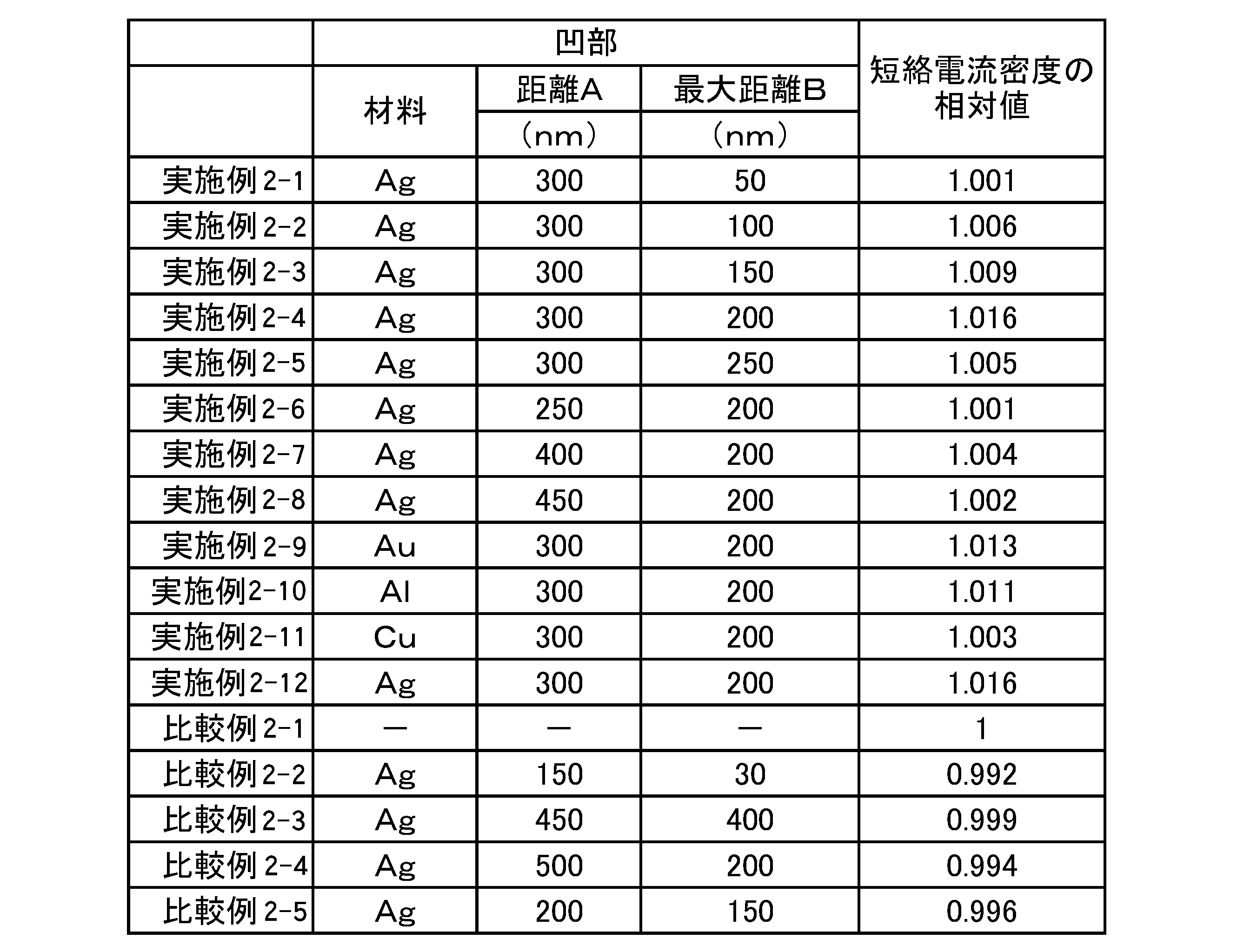
実施例2-1~2-12および比較例2-1~2-5の太陽電池について、擬似太陽光(100mW/cm2)を照射しながら、電流-電位特性を評価した。比較例2-1を基準となる試料とし、実施例2-1~2-12および比較例2-1~2-5の太陽電池について、基準となる試料に対する相対的な短絡電流密度を算出した結果を表2に示す。表2に示すように、実施例2-1~2-12の太陽電池では、比較例2-1~2-5の太陽電池に対して短絡電流密度が顕著に増大しており、実施例2-1~2-12の太陽電池では、光吸収が増大する効果が確認された。
本発明は、上述の実施の形態に限定されるものではなく、当業者の知識に基づいて各種の設計変更等の変形を加えることも可能であり、そのような変形が加えられた実施の形態も本発明の範囲に含まれうるものである。
たとえば、上述した実施の形態では、光電変換層30にp-n接合が形成されているが、光電変換層30は、光電変換が可能な構造であればよく、光電変換層30にp-i-n接合が形成されていてもよい。
10 光電変換素子、20 反射防止層、30 光電変換層、40 透明薄膜層、50 光反射層、52 金属膜、54 貫通部、60 誘電体層、100 マスク、102 開口部、1054 凹部
本発明は、光電変換により光エネルギーを電気エネルギーに変換する光電変換素子に適用することができる。
Claims (15)
- 光電変換層と、
前記光電変換層の一方の主表面側に設けられた金属膜を含む光反射層と、
を備え、
前記金属膜の複数箇所に当該膜の一方の主表面から他方の主表面に貫通する貫通部が設けられていることを特徴とする光電変換素子。 - 任意の前記貫通部の前記光電変換層側の開口における重心と前記任意の前記貫通部に隣接する他の前記貫通部の前記光電変換層側の開口における重心との距離が200~400nmであることを特徴とする請求項1に記載の光電変換素子。
- 前記貫通部の前記光電変換層側の開口において、前記貫通部の内壁の2点間の最大距離が10~250nmであることを特徴とする請求項1または2に記載の光電変換素子。
- 前記光電変換層側の前記金属膜の主表面において、隣接する貫通部間の最短距離が200~400nmであることを特徴とする請求項1乃至3のいずれか1項に記載の光電変換素子。
- 前記光反射層は、400nmから前記光電変換層が発電に利用可能な最大波長の範囲における平均反射率が、40%以上であることを特徴とする請求項1乃至4のいずれか1項に記載の光電変換素子。
- 前記光反射層が、前記光電変換層に対して光受光面とは反対側に備えられていることを特徴とする請求項1乃至5のいずれか1項に記載の光電変換素子。
- 前記金属膜が、Au、Ag、Al、Cuまたはこれらの金属を含む合金からなる請求項1乃至6のいずれか1項に記載の光電変換素子。
- 前記光反射層が、前記金属膜の形成用のマスクを含有する請求項1乃至7のいずれか1項に記載の光電変換素子。
- 前記光反射層が、集電のための裏面電極を兼ねることを特徴とする請求項1乃至8のいずれか1項に記載の光電変換素子。
- 光電変換層と、
前記光電変換層の一方の主表面側に設けられた反射防止層と、
前記光電変換層の他方の主表面側に設けられた金属膜を含む光反射層と、
を備え、
前記金属膜の前記光電変換層の側の主表面に複数の凹部が設けられていることを特徴とする光電変換素子。 - 任意の前記凹部の開口における重心と前記任意の前記凹部に隣接する他の前記凹部の開口における重心との距離が250~400nmであることを特徴とする請求項10に記載の光電変換素子。
- 前記金属膜が、Au、Ag、Al、Cuまたはこれらの金属を含む合金からなる請求項10または11に記載の光電変換素子。
- 前記光電変換層がpn接合を有する単結晶もしくは多結晶シリコンを含むことを特徴とする請求項10乃至12のいずれか1項に記載の光電変換素子。
- 前記光反射層が、前記金属膜の形成用のマスクを含有する請求項10乃至13のいずれか1項に記載の光電変換素子。
- 前記光反射層が、集電のための裏面電極を兼ねることを特徴とする請求項10乃至14のいずれか1項に記載の光電変換素子。
Priority Applications (3)
| Application Number | Priority Date | Filing Date | Title |
|---|---|---|---|
| EP12796471.6A EP2720280A4 (en) | 2011-06-10 | 2012-05-18 | PHOTOELECTRIC CONVERSION ELEMENT |
| CN201280028599.9A CN103597603A (zh) | 2011-06-10 | 2012-05-18 | 光电转换元件 |
| US14/101,455 US20140090705A1 (en) | 2011-06-10 | 2013-12-10 | Photoelectric conversion element |
Applications Claiming Priority (4)
| Application Number | Priority Date | Filing Date | Title |
|---|---|---|---|
| JP2011130574A JP2013004535A (ja) | 2011-06-10 | 2011-06-10 | 光電変換素子 |
| JP2011-130574 | 2011-06-10 | ||
| JP2011-135564 | 2011-06-17 | ||
| JP2011135564A JP2013004805A (ja) | 2011-06-17 | 2011-06-17 | 光電変換素子 |
Related Child Applications (1)
| Application Number | Title | Priority Date | Filing Date |
|---|---|---|---|
| US14/101,455 Continuation US20140090705A1 (en) | 2011-06-10 | 2013-12-10 | Photoelectric conversion element |
Publications (1)
| Publication Number | Publication Date |
|---|---|
| WO2012169123A1 true WO2012169123A1 (ja) | 2012-12-13 |
Family
ID=47295716
Family Applications (1)
| Application Number | Title | Priority Date | Filing Date |
|---|---|---|---|
| PCT/JP2012/003285 Ceased WO2012169123A1 (ja) | 2011-06-10 | 2012-05-18 | 光電変換素子 |
Country Status (5)
| Country | Link |
|---|---|
| US (1) | US20140090705A1 (ja) |
| EP (1) | EP2720280A4 (ja) |
| CN (1) | CN103597603A (ja) |
| TW (1) | TW201304172A (ja) |
| WO (1) | WO2012169123A1 (ja) |
Cited By (1)
| Publication number | Priority date | Publication date | Assignee | Title |
|---|---|---|---|---|
| WO2014199573A1 (ja) * | 2013-06-13 | 2014-12-18 | Jx日鉱日石エネルギー株式会社 | 光電変換素子および光電変換素子の作製方法 |
Families Citing this family (4)
| Publication number | Priority date | Publication date | Assignee | Title |
|---|---|---|---|---|
| TWI573162B (zh) * | 2013-08-22 | 2017-03-01 | 欣興電子股份有限公司 | 光學觸控結構 |
| KR102276913B1 (ko) | 2014-08-12 | 2021-07-13 | 삼성전자주식회사 | 광 다이오드를 가지는 광전 변환 소자 및 광 신호 수신 유닛 |
| GR20150100472A (el) * | 2015-10-30 | 2017-07-03 | Πανεπιστημιο Πατρων | Δισκια πολυκρυσταλλικου πυριτιου με διαμορφωμενες μικροδομες στις επιφανειες τους για την βελτιωση της ηλιακης απορροφησης |
| CN118016745B (zh) * | 2024-04-07 | 2024-10-01 | 浙江晶科能源有限公司 | 太阳能电池及其制备方法、叠层电池及光伏组件 |
Citations (8)
| Publication number | Priority date | Publication date | Assignee | Title |
|---|---|---|---|---|
| JPS59205771A (ja) * | 1983-04-25 | 1984-11-21 | エクソン・リサ−チ・アンド・エンジニアリング・カンパニ− | 太陽電池セル |
| JPS62209872A (ja) * | 1986-03-11 | 1987-09-16 | Fuji Electric Corp Res & Dev Ltd | 光電変換素子 |
| JPH0332445U (ja) * | 1989-08-08 | 1991-03-29 | ||
| JPH05308148A (ja) * | 1992-03-05 | 1993-11-19 | Tdk Corp | 太陽電池 |
| JPH06204537A (ja) * | 1992-12-28 | 1994-07-22 | Canon Inc | 薄膜半導体太陽電池 |
| JP2011109069A (ja) * | 2009-10-23 | 2011-06-02 | Mitsubishi Materials Corp | 導電性反射膜及びその製造方法 |
| JP2011114153A (ja) * | 2009-11-26 | 2011-06-09 | Mitsubishi Electric Corp | 光電変換装置およびその製造方法 |
| WO2011138739A2 (fr) * | 2010-05-05 | 2011-11-10 | Commissariat A L'energie Atomique Et Aux Energies Alternatives | Cellule photovoltaïque à face arrière structurée et procédé de fabrication associé |
Family Cites Families (7)
| Publication number | Priority date | Publication date | Assignee | Title |
|---|---|---|---|---|
| JP2992464B2 (ja) * | 1994-11-04 | 1999-12-20 | キヤノン株式会社 | 集電電極用被覆ワイヤ、該集電電極用被覆ワイヤを用いた光起電力素子及びその製造方法 |
| JP2001036103A (ja) * | 1999-07-15 | 2001-02-09 | Kanegafuchi Chem Ind Co Ltd | アモルファスシリコン系薄膜光電変換装置 |
| US6441298B1 (en) * | 2000-08-15 | 2002-08-27 | Nec Research Institute, Inc | Surface-plasmon enhanced photovoltaic device |
| JP5170110B2 (ja) * | 2008-01-10 | 2013-03-27 | 日本電気株式会社 | 半導体受光素子及び光通信デバイス |
| US20100129949A1 (en) * | 2008-11-25 | 2010-05-27 | Chang Chen | Increasing solar cell efficiency with silver nanowires |
| WO2010150358A1 (ja) * | 2009-06-23 | 2010-12-29 | 三菱電機株式会社 | 光起電力装置およびその製造方法 |
| US8039292B2 (en) * | 2009-11-18 | 2011-10-18 | International Business Machines Corporation | Holey electrode grids for photovoltaic cells with subwavelength and superwavelength feature sizes |
-
2012
- 2012-05-18 WO PCT/JP2012/003285 patent/WO2012169123A1/ja not_active Ceased
- 2012-05-18 EP EP12796471.6A patent/EP2720280A4/en not_active Withdrawn
- 2012-05-18 CN CN201280028599.9A patent/CN103597603A/zh active Pending
- 2012-06-08 TW TW101120635A patent/TW201304172A/zh unknown
-
2013
- 2013-12-10 US US14/101,455 patent/US20140090705A1/en not_active Abandoned
Patent Citations (8)
| Publication number | Priority date | Publication date | Assignee | Title |
|---|---|---|---|---|
| JPS59205771A (ja) * | 1983-04-25 | 1984-11-21 | エクソン・リサ−チ・アンド・エンジニアリング・カンパニ− | 太陽電池セル |
| JPS62209872A (ja) * | 1986-03-11 | 1987-09-16 | Fuji Electric Corp Res & Dev Ltd | 光電変換素子 |
| JPH0332445U (ja) * | 1989-08-08 | 1991-03-29 | ||
| JPH05308148A (ja) * | 1992-03-05 | 1993-11-19 | Tdk Corp | 太陽電池 |
| JPH06204537A (ja) * | 1992-12-28 | 1994-07-22 | Canon Inc | 薄膜半導体太陽電池 |
| JP2011109069A (ja) * | 2009-10-23 | 2011-06-02 | Mitsubishi Materials Corp | 導電性反射膜及びその製造方法 |
| JP2011114153A (ja) * | 2009-11-26 | 2011-06-09 | Mitsubishi Electric Corp | 光電変換装置およびその製造方法 |
| WO2011138739A2 (fr) * | 2010-05-05 | 2011-11-10 | Commissariat A L'energie Atomique Et Aux Energies Alternatives | Cellule photovoltaïque à face arrière structurée et procédé de fabrication associé |
Non-Patent Citations (1)
| Title |
|---|
| See also references of EP2720280A4 * |
Cited By (1)
| Publication number | Priority date | Publication date | Assignee | Title |
|---|---|---|---|---|
| WO2014199573A1 (ja) * | 2013-06-13 | 2014-12-18 | Jx日鉱日石エネルギー株式会社 | 光電変換素子および光電変換素子の作製方法 |
Also Published As
| Publication number | Publication date |
|---|---|
| EP2720280A1 (en) | 2014-04-16 |
| US20140090705A1 (en) | 2014-04-03 |
| TW201304172A (zh) | 2013-01-16 |
| EP2720280A4 (en) | 2015-03-04 |
| CN103597603A (zh) | 2014-02-19 |
Similar Documents
| Publication | Publication Date | Title |
|---|---|---|
| JP7453283B2 (ja) | 半導体基板、太陽電池及び太陽光発電モジュール | |
| JP5147818B2 (ja) | 光電変換装置用基板 | |
| WO2011161961A1 (ja) | 光電変換素子 | |
| JP7498368B2 (ja) | タンデム型太陽光発電デバイス | |
| WO2012169123A1 (ja) | 光電変換素子 | |
| WO2014098146A1 (ja) | 薄膜太陽電池用透光性絶縁基板、および薄膜太陽電池 | |
| KR101729745B1 (ko) | 태양전지 및 이의 제조 방법 | |
| Aurang et al. | Nanowire decorated, ultra-thin, single crystalline silicon for photovoltaic devices | |
| CN119907368A (zh) | 光伏电池及其制造方法、光伏组件 | |
| WO2012160764A1 (ja) | 光電変換素子 | |
| WO2015146333A1 (ja) | 光電変換素子 | |
| KR20150090606A (ko) | 태양 전지 및 이의 제조 방법 | |
| TW201327870A (zh) | 太陽能電池的製備方法 | |
| JP5517775B2 (ja) | 光電変換素子 | |
| TWI470814B (zh) | 太陽能電池 | |
| WO2015015694A1 (ja) | 光起電力装置 | |
| JP6143520B2 (ja) | 結晶シリコン系太陽電池およびその製造方法 | |
| JP5667511B2 (ja) | 光電変換素子 | |
| JP2013004805A (ja) | 光電変換素子 | |
| JP2013004535A (ja) | 光電変換素子 | |
| JP2013219073A (ja) | 光電変換素子 | |
| JP5667510B2 (ja) | 光電変換素子 | |
| CN204375768U (zh) | 基于硅纳米线三维结构的太阳能电池 | |
| KR101373250B1 (ko) | 박막 태양전지 및 그 제조 방법 | |
| TW201327881A (zh) | 太陽能電池 |
Legal Events
| Date | Code | Title | Description |
|---|---|---|---|
| 121 | Ep: the epo has been informed by wipo that ep was designated in this application |
Ref document number: 12796471 Country of ref document: EP Kind code of ref document: A1 |
|
| NENP | Non-entry into the national phase |
Ref country code: DE |
|
| WWE | Wipo information: entry into national phase |
Ref document number: 2012796471 Country of ref document: EP |