WO2012169230A1 - Capteur de fluorescence - Google Patents
Capteur de fluorescence Download PDFInfo
- Publication number
- WO2012169230A1 WO2012169230A1 PCT/JP2012/053692 JP2012053692W WO2012169230A1 WO 2012169230 A1 WO2012169230 A1 WO 2012169230A1 JP 2012053692 W JP2012053692 W JP 2012053692W WO 2012169230 A1 WO2012169230 A1 WO 2012169230A1
- Authority
- WO
- WIPO (PCT)
- Prior art keywords
- fluorescence
- sensor according
- fluorescent sensor
- reflective layer
- sensor
- Prior art date
- Legal status (The legal status is an assumption and is not a legal conclusion. Google has not performed a legal analysis and makes no representation as to the accuracy of the status listed.)
- Ceased
Links
Images




Classifications
-
- G—PHYSICS
- G01—MEASURING; TESTING
- G01N—INVESTIGATING OR ANALYSING MATERIALS BY DETERMINING THEIR CHEMICAL OR PHYSICAL PROPERTIES
- G01N21/00—Investigating or analysing materials by the use of optical means, i.e. using sub-millimetre waves, infrared, visible or ultraviolet light
- G01N21/62—Systems in which the material investigated is excited whereby it emits light or causes a change in wavelength of the incident light
- G01N21/63—Systems in which the material investigated is excited whereby it emits light or causes a change in wavelength of the incident light optically excited
- G01N21/64—Fluorescence; Phosphorescence
- G01N21/6428—Measuring fluorescence of fluorescent products of reactions or of fluorochrome labelled reactive substances, e.g. measuring quenching effects, using measuring "optrodes"
-
- G—PHYSICS
- G01—MEASURING; TESTING
- G01N—INVESTIGATING OR ANALYSING MATERIALS BY DETERMINING THEIR CHEMICAL OR PHYSICAL PROPERTIES
- G01N21/00—Investigating or analysing materials by the use of optical means, i.e. using sub-millimetre waves, infrared, visible or ultraviolet light
- G01N21/62—Systems in which the material investigated is excited whereby it emits light or causes a change in wavelength of the incident light
- G01N21/63—Systems in which the material investigated is excited whereby it emits light or causes a change in wavelength of the incident light optically excited
- G01N21/64—Fluorescence; Phosphorescence
- G01N21/645—Specially adapted constructive features of fluorimeters
- G01N21/6452—Individual samples arranged in a regular 2D-array, e.g. multiwell plates
- G01N21/6454—Individual samples arranged in a regular 2D-array, e.g. multiwell plates using an integrated detector array
Definitions
- the present invention relates to a fluorescence sensor that measures the concentration of an analyte in an aqueous solution, and more particularly, to a fluorescence sensor that includes an indicator that generates fluorescence by an analyte and excitation light.
- Fluorescent sensors that measure the concentration of analytes in liquids, that is, substances to be measured have been developed.
- the fluorescence sensor has an indicator that generates fluorescence with a light amount corresponding to the amount of analyte, and a photoelectric conversion element that detects fluorescence from the indicator.
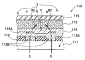
- the fluorescent sensor 110 disclosed in US Pat. No. 5,039,490 can be manufactured using MEMS technology and can be miniaturized.
- the fluorescence sensor 110 includes a transparent substrate 111 that can transmit the excitation light E, a photoelectric conversion element 112 that converts the fluorescence F into an electrical signal, and a condensing light that collects the excitation light E. It is composed of a transparent intermediate layer 115 having a functional part 115A, an indicator 119 that emits a fluorescence F having a light amount corresponding to the amount of analyte by the action of the analyte 2 and the excitation light E, and a light shielding layer 118.
- An object of the present invention is to provide a highly sensitive fluorescent sensor.
- the fluorescence sensor of one embodiment of the present invention includes a photoelectric conversion element that converts fluorescence into an electrical signal, an indicator that generates the fluorescence by an analyte and excitation light, and the analyte disposed on the indicator.
- the fluorescence sensor 40 detects glucose in the body fluid of the subject.
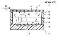
- the fluorescence sensor 40 includes a substrate 11, a filter 13, a light emitting element 14, a transparent intermediate layer 15, an indicator 19, a sensor frame 17, a reflective layer 41, and a light shielding layer.
- the substrate 11 has a structure in which 18 and 18 are sequentially stacked.
- the substrate 11 includes a photodiode element (hereinafter referred to as “PD element”) 12 that is a photoelectric conversion element that converts the fluorescence F into an electric signal.
- the filter 13 disposed so as to cover the PD element 12 transmits the fluorescence F and blocks the excitation light E.
- the light emitting element 14 disposed on the filter 13 generates excitation light E.
- the indicator 19 is made of a hydrogel having a fluorescent dye that generates fluorescence F by the excitation light E and the analyte 2 that has entered after passing through the light shielding layer 18 and the reflection layer 41.
- glucose is the analyte 2.
- the excitation light E generated by the light emitting element 14 is efficiently irradiated to the indicator 19. Further, as shown in FIG. 4, in the fluorescence sensor 40, not only the fluorescence F 1 that directly enters the PD element 12, but also the fluorescence F 2 that has passed through the light emitting element 14 enters the PD element 12. That is, the light emitting element 14 transmits fluorescence. For this reason, the fluorescence sensor 40 is more sensitive than the conventional fluorescence sensor 110 already described.
- the reflective layer 41 disposed in the path of the analyte 2 to the indicator 19 through which the body fluid containing the analyte 2 can pass through the hole is generated by the indicator 19 and emitted in the direction of the reflective layer 41.
- the reflected fluorescence F is reflected in the direction of the PD element 12. That is, the indicator 19 emits fluorescence not only in the direction (downward) of the PD element 12 but also in the upward and sideward directions.
- the fluorescence sensor 40 detects the fluorescence F emitted upward from the indicator 19, that is, in the direction of the reflective layer 41 by the PD element 12.
- the fluorescent sensor 40 can measure the analyte concentration continuously for a predetermined period, for example, one week after being inserted into the body. However, the collected bodily fluid or the bodily fluid circulating through the body via the flow path outside the body may be brought into contact with the fluorescence sensor 40 outside the body without inserting the fluorescence sensor 40 into the body.
- the substrate 11 has a PD element 12.
- a semiconductor substrate of silicon or the like is suitable when the PD element 12 is formed on the substrate by a semiconductor manufacturing technique, but a glass substrate or the like may be used depending on the manufacturing method or arrangement position of the PD element 12.
- a photoconductor, a phototransistor, or the like may be used as the photoelectric conversion element.
- the filter 13 is disposed so as to cover the PD element 12 which is a light receiving unit.
- the filter 13 blocks, for example, the excitation light E having a wavelength of 375 nm generated by the light emitting element 14 disposed on the filter 13, but transmits the fluorescence F having a wavelength of 460 nm generated by the indicator 19.
- the filter 13 may be a multiple interference filter, but is preferably a light absorption filter, for example, a single layer made of silicon, silicon carbide, silicon oxide, silicon nitride, or an organic material, or the single layer It is a multilayer layer formed by laminating.
- the filter 13 may be disposed on the PD element 12 via a transparent protective layer made of, for example, silicon oxide or silicon nitride.
- the filter 13 is preferably disposed as close as possible to the PD element 12 in order to prevent light from entering from the side surface of the protective layer. Further, if there is a space between the PD element 12 and the filter 13, an optical loss occurs and the transmittance decreases. For this reason, it is particularly preferable that the filter 13 is disposed in close contact with the PD element 12.
- an element that transmits fluorescence F is selected from light emitting elements that emit desired excitation light E such as an LED element, an organic EL element, an inorganic EL element, or a laser diode element.
- the light emitting element 14 is an LED element from the viewpoints of fluorescence transmittance, light generation efficiency, wide wavelength selectivity of the excitation light E, and generation of only light other than the wavelength having the excitation action. preferable. Further, among LED elements, an ultraviolet LED element made of a gallium nitride-based compound semiconductor formed on a sapphire substrate having high fluorescence F transmittance is particularly preferable.
- the transparent intermediate layer 15 disposed on the light emitting element 14 is required to have good electrical insulation, moisture barrier properties, light transmittance with respect to excitation light E and fluorescence F, and the like. Further, as a characteristic of the transparent intermediate layer 15, it is important that the generation of the fluorescence F is small even when the excitation light E is irradiated, that is, it is difficult to emit autofluorescence.
- quartz, glass, silicone resin, or transparent amorphous fluororesin is preferably used, and among them, silicone resin or transparent amorphous fluororesin is particularly preferable.
- the indicator 19 is made of a hydrogel having a fluorescent dye that generates fluorescence F having a wavelength longer than that of the excitation light E by the analyte 2 and the excitation light E.
- the indicator 19 is composed of a hydrogel that contains the fluorescent dye that generates the fluorescence F with a light amount corresponding to the analyte concentration in the sample and that allows the excitation light E and the fluorescence F to pass therethrough satisfactorily.
- the indicator 19 may be the analyte 2 itself in which the fluorescent dye that does not contain the fluorescent dye and generates the fluorescent F exists in the solution.
- Hydrogel is water such as acrylic hydrogel prepared by polymerizing monomers such as polysaccharides such as methylcellulose or dextran, acrylamide, methylol acrylamide, hydroxyethyl acrylate, or urethane hydrogel prepared from polyethylene glycol and diisocyanate. It is formed by encapsulating a fluorescent dye in a material that is easy to contain.
- the hydrogel has a size that does not leave the sensor via the light shielding layer 18 / reflective layer 41.
- the hydrogel has a molecular weight of 4 million or more, or is in the form of particles having a diameter of 50 nm or more, for example, greater than or equal to the outer diameter D of the through-hole of the reflective layer 41, or in a form that is crosslinked and does not flow.
- phenylboronic acid derivatives having a fluorescent residue are suitable as fluorescent dyes.
- the fluorescent dye is prevented from detaching from the sensor by using a high molecular weight material or chemically fixing to a hydrogel.
- the indicator 19 is produced by polymerizing a phosphoric acid buffer containing a fluorescent dye, a gel skeleton-forming material, and a polymerization initiator in a nitrogen atmosphere for 1 hour.
- a fluorescent dye 9,40-bis [N- [2- (5,5-dimethylborinan-2-yl) benzyl] -N- [6 ′-[(acryloylpolyethyleneglycol-3400) carbonylamino ] -N-hexylamino] methyl] -2-acetylanthracene (F-PEG-AAm), acrylamide as the gel skeleton-forming material, sodium peroxodisulfate and N, N, N ′ as the polymerization initiator N'-tetramethylethylenediamine is used.
- the indicator 19 it is also possible to use a gel-like or liquid-like hydrogel containing a fluorescent dye, which is accommodated in an indicator space composed of the transparent intermediate layer 15, the reflective layer 41, and the sensor frame 17. .
- the reflective layer 41 has a function of reflecting the fluorescence F and further protecting the indicator 19.
- the reflection layer 41 uses a metal, an inorganic compound, or an organic compound that has a high reflectance with respect to fluorescence, but a metal or an alloy such as Al, Au, Ag, Pt, Cr, or Ti is particularly preferable.
- the reflective layer 41 has a through hole through which the body fluid containing the analyte 2 can pass.
- the through-holes may be formed uniformly in the reflective layer 41, may be formed locally in a partial region, or may be formed randomly.
- the internal shape of the through hole may be a columnar shape, a prismatic shape, or a polygonal shape.
- the outer dimension (diameter) D of the through hole is such that leakage of the excitation light E and the fluorescence F to the outside of the fluorescence sensor 40 is minimized in addition to being able to pass the body fluid containing the analyte 2.
- the diameter is preferably equal to or less than the wavelength of ultraviolet to blue excitation light. That is, the outer dimension (outer diameter) D of the through hole is preferably 10 nm to 350 nm.
- the outer dimension is the maximum length of the opening of the hole, and is the diameter when the opening is circular.
- the light shielding layer 18 prevents light leakage and at the same time prevents outside light from entering the inside of the fluorescence sensor.
- the light shielding layer 18 has biocompatibility and does not prevent passage of body fluid containing the analyte 2.
- the light shielding layer 18 is made of, for example, a porous metal or ceramic, or a composite material in which a hydrogel used for the indicator 19 is mixed with fine particles that do not transmit light such as carbon black or carbon nanotubes.
- the reflective layer 41 and the indicator 19 are preferably disposed in close contact with each other, but may be disposed through an intermediate layer (not shown) through which a body fluid containing an analyte can pass.
- the intermediate layer is preferably a solid layer made of quartz, glass, fluorine or silicone resin, but may be a liquid layer or space such as an aqueous solution through which the analyte can pass.
- the sensor frame 17 has a function of protecting the sensor main body and a light shielding function, that is, a function of preventing external light from entering and preventing light from leaking from the inside of the sensor to the outside of the sensor.
- the sensor frame 17 is preferably made of a highly rigid material in order to protect the sensor body.
- the sensor frame 17 is made of a resin material such as silicon, glass or metal having a Young's modulus of several tens to several hundreds of GPa, or polypropylene or polystyrene having a Young's modulus of about 1 GPa to 5 GPa.
- the sensor frame 17 is blackened by mixing carbon black or the like in order to improve the light shielding function.
- the sensor frame 17 may be manufactured from a part of the substrate by processing the substrate 11.
- the fluorescence F3 and F4 reflected by the reflection layer 41 out of the fluorescence generated by the fluorescent dye of the indicator 19 in various directions also enter the PD element 12. Since more fluorescence is incident on the PD element 12, the fluorescence sensor 40 is highly sensitive.
- the fluorescence sensor 40A of the second embodiment is similar to the fluorescence sensor 40, the same components are denoted by the same reference numerals and description thereof is omitted.
- the reflection layer 41A is formed of a multilayer film in which a plurality of layers are laminated and that selectively reflects the fluorescence wavelength.
- the reflective layer 41A has a plurality of holes formed by an etching method through which an analyte can pass.
- high refractive index layers and low refractive index layers are alternately stacked, and selectively reflects fluorescence due to light interference effects.
- silicon nitride 2.0
- silicon oxide 1.41 to 1.45
- the high refractive index and the low refractive index are not high or low in the absolute value of the refractive index of the two layers, but indicate a relative relationship. That is, when the refractive index of the high refractive index layer (first transparent layer) is n1 and the refractive index of the low refractive index layer (second transparent layer) is n2, n1> n2, preferably n1-n2> 0. .5 is sufficient.
- a three-layer reflective layer 41A composed of two silicon nitride layers with a thickness of 250 nm as high refractive index layers and one silicon oxide layer with a thickness of 170 nm as low refractive index layers has a wavelength of 460 nm.
- the reflectance for the fluorescent light of 60% is 60%
- the reflectance for the excitation light having a wavelength of 375 nm is 25%. That is, the reflective layer 41A selectively reflects fluorescence.
- the fluorescent sensor 40A including the reflective layer 41A has the same effect as the fluorescent sensor 40, and the reflective layer 41A selectively reflects fluorescence, and thus has higher sensitivity.
- the reflective layer 41B has a structure in which high reflectance particles 43 are embedded in a porous base material through which the analyte can pass.
- the reflective layer 41 ⁇ / b> B is made of a porous material containing a plurality of high reflectivity particles 43.
- the porous material means a material having voids and pores connected to the outside in the structure.
- the size, distribution, and shape of the voids / pores need not be regular as long as the body fluid containing the analyte can pass therethrough, and can be appropriately selected.
- the open porosity of the base material is preferably 5 to 75% by volume, particularly preferably 20 to 50% by volume. If it is more than the said range, a bodily fluid will pass easily, and if it is less than the said range, desired mechanical strength will be obtained.
- the open porosity is a value measured by Archimedes method.
- the base material of the reflective layer 41B for example, cellulose or polyacrylamide is used.
- the high reflectivity particles 43 are high reflectivity metals, ceramics, organic material spheres coated with white on the surface, and the like.
- the high reflectance particle 43 is a particle that reflects incident light when the reflectance with respect to fluorescence is 50% or more, preferably 70% or more.
- the particle diameter d of the high reflectance particles 43 is preferably about 1 ⁇ 2 of the fluorescence wavelength ⁇ .
- the particle size is a median value measured by a laser diffraction method, that is, a peak value of the particle size distribution.
- the high reflectance particle 43 when the particle size d is 1 ⁇ 2 of the wavelength ⁇ , the high reflectance particle 43 has the maximum light scattering efficiency and the light hiding power and the maximum reflection efficiency.
- the high-reflectivity particles 43 having a particle diameter of 1 ⁇ 2 of the fluorescence wavelength strongly reflect fluorescence, but do not reflect excitation light E having a wavelength lower than that of fluorescence. That is, since the high reflectance particles 43 having a particle diameter of 1 ⁇ 2 of the fluorescence wavelength selectively reflect fluorescence, the S / N ratio of light incident on the PD element is improved.
- the particle diameter of the high reflectivity particles 43 is preferably exactly 1/2 ( ⁇ / 2) of the fluorescence wavelength, but the above effect can be obtained when ( ⁇ / 2) ⁇ 10%.
- the particle diameter d may be 230 nm ⁇ 10%, that is, 207 to 253 nm ⁇ Table 1>
- the manufacturing method is preferable because the hydrochloric acid method has a more uniform particle size than the sulfuric acid method.
- the reflective layer 41B introduces the high reflectance particles 43 simultaneously when manufacturing the base material.
- the fluorescent sensor 40B has the effect of the fluorescent sensor 40, and the reflective layer 41B does not require through-hole formation or multilayer film production, so the manufacturing cost is low.
- the fluorescence sensor 40C includes a reflective layer (second reflective layer) 42 on the side surface of the indicator 19. Similar to the reflective layer 41, the second reflective layer 42 reflects the fluorescence generated by the indicator 19 and makes it incident on the PD element. However, unlike the reflective layer 41, it is not necessary that body fluid can pass through.
- the second reflective layer 42 is disposed on the inner surface of the sensor frame 17 using the same material as that of the reflective layer 41, but need not be the same material.
- the second reflective layer 42 may be bonded to the sensor frame 17 via an adhesive, or may be directly formed.
- a transparent protective layer may be formed on the second reflective layer 42.
- the fluorescence F5 reflected by the second reflective layer 42 among the fluorescence generated by the indicator 19 also enters the PD element 12.
- the fluorescence sensor 40C has the same effect as the fluorescence sensor 40, and is more sensitive because more fluorescence is incident on the PD element 12.
- the sensor frame 17 may be provided with the function of the second reflective layer 42 by mirror-finishing the inner surface of the sensor frame 17 so as to reflect fluorescence.
- the fluorescence sensors 40, 40A, and 40B it is possible to achieve higher sensitivity by providing the reflective layer (second reflective layer) 42 on the side surface of the indicator 19 like the fluorescent sensor 40C.
- the fluorescence sensor 40D has a structure similar to that of the conventional fluorescence sensor 110.
- the fluorescence sensor 40F includes a transparent substrate 11D, and excitation light E that has passed through the gap 12B of the PD element substrate 12A enters the indicator 19 from the lower surface of the transparent substrate 11D.
- the excitation light E passes through the transparent substrate 11 ⁇ / b> D / gap 12 ⁇ / b> B, enters the transparent intermediate layer 15, is condensed by the condensing function unit 15 ⁇ / b> D disposed in the transparent intermediate layer 15, and enters the indicator 19.
- the fluorescence of the intensity corresponding to the amount of the analyte present in the indicator 19 is directed in various directions by the interaction between the excitation light and the analyte 2 that has entered through the light shielding layer 18 and the reflective layer 41. Radiates radially. Among these, the fluorescence F2 emitted in the direction of the PD element 12D directly enters the PD element 12D.
- the fluorescence F4 emitted from the indicator 19 in the direction opposite to the PD element 12D is reflected by the reflective layer 41 toward the PD element 12D and enters the PD element 12D. Since the PD element 12D outputs an electrical signal corresponding to the amount of incident fluorescence, the output of the fluorescence sensor 40D is increased by the amount of fluorescence F3 and F4 compared to a fluorescence sensor without a reflective layer.
- Fluorescent sensor 40D has the same effect as fluorescent sensor 40. That is, the amount of fluorescent light received by the PD element 12D increases and the sensor output increases. Therefore, the sensitivity is higher than that of a conventional fluorescent sensor, and it is possible to accurately detect an analyte and to detect even a small amount of analyte with high accuracy.
- a metal having a through hole, a laminated film of a high refractive index layer and a low refractive index layer, and a porous material containing high reflectance particles are used as the reflective layer.
- a second reflective layer that reflects fluorescence may be disposed on the side surface of the indicator 19.
- the fluorescence sensor 40E of the sixth embodiment is similar to the fluorescence sensor 40, the same components are denoted by the same reference numerals and description thereof is omitted.
- the PD element 12 is disposed on the side surface side of the indicator 19.
- the PD element 12E is formed on the side surface of the recess formed in the substrate 11E made of a semiconductor such as silicon, and the light emitting element 14 is disposed on the bottom surface of the recess.
- the opening surface of the recess is wider than the bottom surface, and the side surface is not perpendicular to the bottom surface but is inclined at a predetermined angle ⁇ .
- substrate 11E which has a recessed part may be produced by joining the frame-shaped sensor frame used as a recessed part, and a planar substrate.
- an indicator 19 is disposed in a concave portion of the transparent intermediate layer 15 covering the PD element 12E and the filter 13E, and the concave portion is sealed by the reflective layer 41 and the light shielding layer 18.
- the fluorescence sensor 40E will be briefly described. In addition, although it may manufacture for every one fluorescence sensor 40E, it is preferable to manufacture many sensors collectively as a wafer process.
- a mask layer having a plurality of mask portions on the first main surface of a silicon wafer having an area where a plurality of elements can be manufactured is manufactured. And the some recessed part with a bottom face parallel to a main surface is formed by the etching method.
- etching method a wet etching method using a tetramethylammonium hydroxide (TMAH) aqueous solution, a potassium hydroxide (KOH) aqueous solution, or the like is preferable, but dry etching such as reactive ion etching (RIE) or chemical dry etching (CDE) is used.
- TMAH tetramethylammonium hydroxide
- KOH potassium hydroxide
- CDE chemical dry etching
- the PD element 12E is formed on the side surface of each recess by a known semiconductor process.
- the side surface may be vertical, but the inclined concave portion not only has a larger area for forming the PD element 12 than the concave portion with the vertical side surface, but also facilitates the formation of the PD element 12 on the side surface. If the inclination angle of the side surface is 30 to 70 degrees, the above effect is remarkable.
- the filter 13E is disposed on the side PD element 12E.
- a transparent protective layer such as a silicon oxide layer may be formed on the filter 13E.
- the light emitting elements 14 are respectively disposed on the bottom surfaces of the plurality of recesses.
- the indicator 19 is disposed in the recess.
- the reflective layer 41 and the light shielding layer 18 are disposed so as to close the opening of the recess.
- the silicon wafer on which the plurality of sensors are formed is separated into pieces, and the fluorescence sensor 40E is completed.
- the fluorescent sensor 40E has the same effects as the fluorescent sensor 40 and the like, and the substrate 11E also serves as a sensor frame, and the side surface of the concave portion that is the PD element forming surface is inclined, so that the manufacturing is easy.
- the shape of the whole fluorescence sensor demonstrated in the said several embodiment was a right-angled column shape, it is a trapezoid shape, the shape where the side surface curved, or the needle-type fluorescence sensor etc. which extended one direction of the sensor side surface etc. There may be.
- the fluorescence sensor can respond
Landscapes
- Health & Medical Sciences (AREA)
- Immunology (AREA)
- Chemical & Material Sciences (AREA)
- Physics & Mathematics (AREA)
- Biochemistry (AREA)
- Nuclear Medicine, Radiotherapy & Molecular Imaging (AREA)
- Life Sciences & Earth Sciences (AREA)
- Analytical Chemistry (AREA)
- General Health & Medical Sciences (AREA)
- General Physics & Mathematics (AREA)
- Pathology (AREA)
- Optics & Photonics (AREA)
- Chemical Kinetics & Catalysis (AREA)
- Investigating, Analyzing Materials By Fluorescence Or Luminescence (AREA)
Abstract
L'invention concerne un capteur de fluorescence (10) qui comprend : un élément PD (12) destiné à convertir une fluorescence (F) en un signal électrique ; un indicateur (19) destiné à générer la fluorescence (F) à l'aide d'un analyte (2) et d'une lumière d'excitation (E0) ; et une surface réfléchissante (41) disposée sur l'indicateur (19) et agencée pour réfléchir la fluorescence (F) dans la direction de l'élément PD (12), permettant à un fluide corporel contenant l'analyte (2) de passer à travers la couche réfléchissante.
Applications Claiming Priority (2)
| Application Number | Priority Date | Filing Date | Title |
|---|---|---|---|
| JP2011-128627 | 2011-06-08 | ||
| JP2011128627 | 2011-06-08 |
Publications (1)
| Publication Number | Publication Date |
|---|---|
| WO2012169230A1 true WO2012169230A1 (fr) | 2012-12-13 |
Family
ID=47295804
Family Applications (1)
| Application Number | Title | Priority Date | Filing Date |
|---|---|---|---|
| PCT/JP2012/053692 Ceased WO2012169230A1 (fr) | 2011-06-08 | 2012-02-16 | Capteur de fluorescence |
Country Status (1)
| Country | Link |
|---|---|
| WO (1) | WO2012169230A1 (fr) |
Cited By (1)
| Publication number | Priority date | Publication date | Assignee | Title |
|---|---|---|---|---|
| WO2021208978A1 (fr) * | 2020-04-15 | 2021-10-21 | Highfly Therapeutics (Hk) Limited | Système et procédé de détection de fluorescence |
Citations (6)
| Publication number | Priority date | Publication date | Assignee | Title |
|---|---|---|---|---|
| JPH0526876A (ja) * | 1991-07-24 | 1993-02-02 | Fuji Photo Film Co Ltd | 全血試料分析用乾式分析要素 |
| JPH11500825A (ja) * | 1995-02-21 | 1999-01-19 | アーサー・イー・コルヴィン・ジュニアー | 光学式螢光センサ |
| JP2001525930A (ja) * | 1997-05-13 | 2001-12-11 | コルビン,アーサー・イー・ジュニア | 改良された蛍光検出デバイス |
| JP2002523774A (ja) * | 1998-08-26 | 2002-07-30 | センサーズ・フォー・メデセン・アンド・サイエンス・インコーポレーテッド | 光学式検知装置 |
| WO2004071291A2 (fr) * | 2003-02-13 | 2004-08-26 | Medtronic, Inc. | Detecteur chimique implantable |
| WO2010119916A1 (fr) * | 2009-04-13 | 2010-10-21 | Olympus Corporation | Capteur de fluorescence, capteur de fluorescence de type aiguille et procédé pour mesurer un analyte |
-
2012
- 2012-02-16 WO PCT/JP2012/053692 patent/WO2012169230A1/fr not_active Ceased
Patent Citations (6)
| Publication number | Priority date | Publication date | Assignee | Title |
|---|---|---|---|---|
| JPH0526876A (ja) * | 1991-07-24 | 1993-02-02 | Fuji Photo Film Co Ltd | 全血試料分析用乾式分析要素 |
| JPH11500825A (ja) * | 1995-02-21 | 1999-01-19 | アーサー・イー・コルヴィン・ジュニアー | 光学式螢光センサ |
| JP2001525930A (ja) * | 1997-05-13 | 2001-12-11 | コルビン,アーサー・イー・ジュニア | 改良された蛍光検出デバイス |
| JP2002523774A (ja) * | 1998-08-26 | 2002-07-30 | センサーズ・フォー・メデセン・アンド・サイエンス・インコーポレーテッド | 光学式検知装置 |
| WO2004071291A2 (fr) * | 2003-02-13 | 2004-08-26 | Medtronic, Inc. | Detecteur chimique implantable |
| WO2010119916A1 (fr) * | 2009-04-13 | 2010-10-21 | Olympus Corporation | Capteur de fluorescence, capteur de fluorescence de type aiguille et procédé pour mesurer un analyte |
Cited By (2)
| Publication number | Priority date | Publication date | Assignee | Title |
|---|---|---|---|---|
| WO2021208978A1 (fr) * | 2020-04-15 | 2021-10-21 | Highfly Therapeutics (Hk) Limited | Système et procédé de détection de fluorescence |
| US20230143114A1 (en) * | 2020-04-15 | 2023-05-11 | Hifibio (Hk) Limited | A system and a method for fluorescence detection |
Similar Documents
| Publication | Publication Date | Title |
|---|---|---|
| CN103884696A (zh) | 分光计组件及方法 | |
| TW201840999A (zh) | 垂直腔表面發射雷射低發散角近接感測器 | |
| JP2006126715A (ja) | 光導波路およびこの光導波路を用いた蛍光センサ | |
| US20130037727A1 (en) | Fluorescence sensor | |
| JP2002527771A (ja) | 誘電体積層膜を備えた光センサ | |
| TW201003059A (en) | Sensor chip for biological and chemical sensing | |
| WO2012056989A1 (fr) | Capteur de fluorescence | |
| JP6087337B2 (ja) | 蛍光センサおよびセンサシステム | |
| CN108885176A (zh) | 具有纳米多孔表面层的波导传感器 | |
| US9046484B2 (en) | Plasmon sensor | |
| JP2015114219A (ja) | 電場増強素子、分析装置、及び電子機器 | |
| JP4673714B2 (ja) | 光導波路型バイオケミカルセンサチップおよびその製造方法 | |
| JP2015064205A (ja) | 局在プラズモン共鳴チップ及びこれを用いた局在プラズモン共鳴バイオセンサ | |
| CN215985737U (zh) | 柔性共振型光学芯片及应用该芯片的传感器 | |
| JP4823330B2 (ja) | 光導波路型バイオケミカルセンサチップ及びその測定対象物の測定方法 | |
| JP2014525051A (ja) | 目標要素への光の集光 | |
| KR101109148B1 (ko) | 표면 플라즈몬 공진 센서 및 표면 플라즈몬 공진을 이용한 센싱 방법 | |
| JP6127278B2 (ja) | 光学的センサと、光学的センサを用いた検出方法と、捕捉体の固定方法と、検査ユニット | |
| JP2015010825A (ja) | 局在プラズモン共鳴チップ | |
| KR101240294B1 (ko) | 실리콘 나노와이어 바이오센서 모듈 | |
| JP2012058218A5 (fr) | ||
| CH708389A2 (fr) | Cartouche de mesure par fluorescence pour diagnostic biomédical. | |
| TW200837345A (en) | Planar surface plasma resonance sensor | |
| JP4560105B2 (ja) | 小型化表面プラズモン共振感知チップ | |
| JP5728419B2 (ja) | センサチップ、測定装置、および測定方法 |
Legal Events
| Date | Code | Title | Description |
|---|---|---|---|
| 121 | Ep: the epo has been informed by wipo that ep was designated in this application |
Ref document number: 12796693 Country of ref document: EP Kind code of ref document: A1 |
|
| NENP | Non-entry into the national phase |
Ref country code: DE |
|
| 122 | Ep: pct application non-entry in european phase |
Ref document number: 12796693 Country of ref document: EP Kind code of ref document: A1 |
|
| NENP | Non-entry into the national phase |
Ref country code: JP |