WO2012169401A1 - Dispositif à relais à semi-conducteurs pour l'isolement du courant continu - Google Patents
Dispositif à relais à semi-conducteurs pour l'isolement du courant continu Download PDFInfo
- Publication number
- WO2012169401A1 WO2012169401A1 PCT/JP2012/063902 JP2012063902W WO2012169401A1 WO 2012169401 A1 WO2012169401 A1 WO 2012169401A1 JP 2012063902 W JP2012063902 W JP 2012063902W WO 2012169401 A1 WO2012169401 A1 WO 2012169401A1
- Authority
- WO
- WIPO (PCT)
- Prior art keywords
- signal
- voltage
- relay
- mosfets
- semiconductor relay
- Prior art date
- Legal status (The legal status is an assumption and is not a legal conclusion. Google has not performed a legal analysis and makes no representation as to the accuracy of the status listed.)
- Ceased
Links
Images



Classifications
-
- H—ELECTRICITY
- H03—ELECTRONIC CIRCUITRY
- H03K—PULSE TECHNIQUE
- H03K17/00—Electronic switching or gating, i.e. not by contact-making and –breaking
- H03K17/94—Electronic switching or gating, i.e. not by contact-making and –breaking characterised by the way in which the control signals are generated
- H03K17/941—Electronic switching or gating, i.e. not by contact-making and –breaking characterised by the way in which the control signals are generated using an optical detector
-
- G—PHYSICS
- G01—MEASURING; TESTING
- G01J—MEASUREMENT OF INTENSITY, VELOCITY, SPECTRAL CONTENT, POLARISATION, PHASE OR PULSE CHARACTERISTICS OF INFRARED, VISIBLE OR ULTRAVIOLET LIGHT; COLORIMETRY; RADIATION PYROMETRY
- G01J1/00—Photometry, e.g. photographic exposure meter
- G01J1/42—Photometry, e.g. photographic exposure meter using electric radiation detectors
- G01J1/44—Electric circuits
- G01J1/46—Electric circuits using a capacitor
-
- G—PHYSICS
- G01—MEASURING; TESTING
- G01J—MEASUREMENT OF INTENSITY, VELOCITY, SPECTRAL CONTENT, POLARISATION, PHASE OR PULSE CHARACTERISTICS OF INFRARED, VISIBLE OR ULTRAVIOLET LIGHT; COLORIMETRY; RADIATION PYROMETRY
- G01J5/00—Radiation pyrometry, e.g. infrared or optical thermometry
- G01J5/10—Radiation pyrometry, e.g. infrared or optical thermometry using electric radiation detectors
- G01J5/34—Radiation pyrometry, e.g. infrared or optical thermometry using electric radiation detectors using capacitors, e.g. pyroelectric capacitors
-
- H—ELECTRICITY
- H03—ELECTRONIC CIRCUITRY
- H03K—PULSE TECHNIQUE
- H03K17/00—Electronic switching or gating, i.e. not by contact-making and –breaking
- H03K17/51—Electronic switching or gating, i.e. not by contact-making and –breaking characterised by the components used
- H03K17/56—Electronic switching or gating, i.e. not by contact-making and –breaking characterised by the components used by the use, as active elements, of semiconductor devices
- H03K17/687—Electronic switching or gating, i.e. not by contact-making and –breaking characterised by the components used by the use, as active elements, of semiconductor devices the devices being field-effect transistors
- H03K17/6871—Electronic switching or gating, i.e. not by contact-making and –breaking characterised by the components used by the use, as active elements, of semiconductor devices the devices being field-effect transistors the output circuit comprising more than one controlled field-effect transistor
- H03K17/6874—Electronic switching or gating, i.e. not by contact-making and –breaking characterised by the components used by the use, as active elements, of semiconductor devices the devices being field-effect transistors the output circuit comprising more than one controlled field-effect transistor in a symmetrical configuration
-
- H—ELECTRICITY
- H03—ELECTRONIC CIRCUITRY
- H03K—PULSE TECHNIQUE
- H03K17/00—Electronic switching or gating, i.e. not by contact-making and –breaking
- H03K17/51—Electronic switching or gating, i.e. not by contact-making and –breaking characterised by the components used
- H03K17/56—Electronic switching or gating, i.e. not by contact-making and –breaking characterised by the components used by the use, as active elements, of semiconductor devices
- H03K17/687—Electronic switching or gating, i.e. not by contact-making and –breaking characterised by the components used by the use, as active elements, of semiconductor devices the devices being field-effect transistors
- H03K17/689—Electronic switching or gating, i.e. not by contact-making and –breaking characterised by the components used by the use, as active elements, of semiconductor devices the devices being field-effect transistors with galvanic isolation between the control circuit and the output circuit
-
- G—PHYSICS
- G08—SIGNALLING
- G08B—SIGNALLING SYSTEMS, e.g. PERSONAL CALLING SYSTEMS; ORDER TELEGRAPHS; ALARM SYSTEMS
- G08B13/00—Burglar, theft or intruder alarms
- G08B13/18—Actuation by interference with heat, light, or radiation of shorter wavelength; Actuation by intruding sources of heat, light, or radiation of shorter wavelength
- G08B13/189—Actuation by interference with heat, light, or radiation of shorter wavelength; Actuation by intruding sources of heat, light, or radiation of shorter wavelength using passive radiation detection systems
- G08B13/19—Actuation by interference with heat, light, or radiation of shorter wavelength; Actuation by intruding sources of heat, light, or radiation of shorter wavelength using passive radiation detection systems using infrared-radiation detection systems
Definitions
- the present invention relates to a direct current insulation type semiconductor relay device having two MOSFETs connected in series.
- a photo MOS relay that performs an on / off operation by applying light from a light emitting diode (LED) to a photodiode array and conducting a gate of a MOSFET (for example, Patent Document 1).
- a signal input circuit and a relay circuit are optically coupled, and the input and output are electrically insulated.
- Patent Document 2 Also known are two MOSFETs in which a signal input circuit and a relay circuit are insulated and separated by a transformer or DC-isolated by a capacitor (for example, Patent Document 2).
- a semiconductor relay device is used in a configuration of a switch device incorporating the same and a control panel (CP) that is a relay output side device that receives a relay output and also supplies power to the switch device. If at least direct current (DC) insulation is possible from the viewpoint of (CP), circuit dependency with the switch device is eliminated, and protection from electrical influences is achieved.
- DC direct current
- the above-described semiconductor relay device is incorporated in a switch device that needs to be silent during relay operation, for example, in an object detection sensor that detects an object, and is used for relay driving based on object detection under the control of a microcomputer (MC). Based on the AC signal, the MOSFET is turned on / off, and a detection on / off signal is output to the control panel (CP).
- MC microcomputer
- JP 2009-004522 A Japanese Patent Publication No. 2-30206
- the above-described photo MOS relay needs to be molded with a light-shielding resin in order to prevent the input of unnecessary external light after the optical system is formed of a transparent resin, which increases the cost.
- the control panel (CP) has a common type such as a GND common type and a common power source type. Depending on the type, the switch device including the conventional semiconductor relay device may not be properly connected. There was a problem that it was difficult.
- the present invention solves the above-mentioned problems, enables reliable operation and cost reduction, can be connected regardless of the type of the relay output side device, and can be used for general purposes.
- the purpose is to provide.
- a DC insulation type semiconductor relay device includes a signal input unit that inputs an AC signal for driving a relay, a DC insulation member that blocks a DC current among the AC signals, A voltage doubler circuit that doubles the signal voltage after interruption of the DC current to an integral multiple; and a relay circuit that includes two MOSFETs that are connected in reverse series with their sources connected, and with their gates connected, By making the gates of the two MOSFETs conductive by a signal whose voltage is doubled by the voltage doubler circuit, the two MOSFETs are bidirectionally turned on and off.
- the circuit dependency of the relay output side device is reduced by realizing the DC insulation between the signal input unit and the relay circuit. Since the voltage doubler circuit doubles the signal voltage after DC current interruption to an integral multiple, the voltage doubled signal is made to conduct to each gate so that the signal voltage can be reduced. Can be operated stably. Therefore, reliable operation and cost reduction of the device are possible, and connection is possible regardless of the type of the relay output side device and it can be used for general purposes.
- the DC insulating member is a capacitor or a transformer. Therefore, DC insulation can be performed at low cost.
- the voltage doubler circuit is a double or triple voltage doubler circuit. Therefore, more reliable operation is possible.
- the MOSFET is turned on / off by driving with the alternating current signal based on the object detection, and a detection on / off signal is sent to a relay output device. Is output.
- the device can be matched with a low voltage microcomputer.
- the object detection sensor is a security sensor.
- FIG. 1 is a side view showing an object detection sensor 10 which is a switch device incorporating a DC insulation type semiconductor relay device 1 according to an embodiment of the present invention.
- the control panel (CP) 8 is a relay output side device that receives a relay output from the object detection sensor 10 and supplies power to the object detection sensor 10.
- CP8 is a GND common type in which GND (ground) is common in a connection state in which power is supplied to the semiconductor relay device 1.
- the object detection sensor 10 is, for example, a PIR (passive infrared ray) sensor attached to a ceiling, and a corresponding sensor unit in which infrared energy radiated from a human body H or the like entering in a detection area is condensed by an optical system.
- the detection signal incident on the (pyroelectric element) 12 and detected by the pyroelectric element 12 is subjected to signal detection processing under the control of the microcomputer (MC) 15 to detect the intruder H.
- MC microcomputer
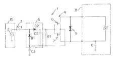
- FIG. 2 is a circuit diagram showing an example of a configuration including a DC insulation type semiconductor relay device 1 according to an embodiment of the present invention.
- the device 1 doubles the signal input unit 2 for inputting an AC signal for driving the relay, the DC insulating member 3 for blocking the DC current among the AC signals, and the signal voltage after the DC current is interrupted.
- the voltage doubler circuit 5 and the relay circuit 4 including two n-type MOSFETs 6 and 7, which are connected in reverse series with the sources S connected to each other and the gates G are protected, and the MOSFETs 6 and 7 are protected.
- a protection circuit 9. In place of the n-type MOSFET, a p-type MOSFET may be used.
- the signal input unit 2 relays based on the detection of the intruder H under the control of the microcomputer (MC) 15.
- a driving AC signal (rectangular wave output) is input to the DC insulating member 3.
- the MC 15 has a low drive voltage to reduce power consumption.
- the drive voltage is set to 2 V by a regulator (not shown) with respect to the voltage 12 v from the power supply Vcc of the CP 8 to detect the intruder H, for example. 2V AC signal is input to the voltage doubler circuit 5 through the DC insulating member 3.
- the DC insulating member 3 is, for example, a capacitor C1, and performs direct current (DC) insulation between the signal input unit 2 and the relay circuit 4 to supply power by AC coupling.
- DC direct current
- a transformer can be used as the DC insulating member 3 instead of the capacitor C1.
- cost reduction can be achieved compared with the transformer of winding structure.
- the inductance of the transformer can be kept small.
- the voltage doubler circuit 5 includes, for example, a second diode D2 connected in series with a capacitor C1 that is a DC insulating member 3, a first diode D1 connected in parallel to both ends of the second diode D2, and a voltage doubler capacitor C2. And a capacitor C3 connected between the first diode D1 and the voltage doubler capacitor C2 and grounded.
- the cathode of the first diode D1 and the anode of the second diode D2 are connected, and the cathode of the first diode D1 and the capacitor C3 are connected.
- the first diode D1 conducts and charges the capacitor C3 when the negative voltage of the AC signal is DC-insulated, and the second diode D2 conducts and discharges the capacitor C3 when the positive voltage is applied, and charges the voltage doubler capacitor C2.
- the signal voltage having the same voltage level and the same voltage level as the generated voltage is generated, and a double signal voltage is generated.
- One end 21 of the output terminal of the voltage doubler circuit 5 and a connection point 23 of the gates G of the two MOSFETs 6 and 7 are connected, and the other end 22 of the output terminal and a connection point 24 of the source S of the two MOSFETs 6 and 7 are connected.
- each gate G is turned on by a signal whose voltage is doubled by the voltage doubler circuit 5, thereby turning on and off the two MOSFETs 6 and 7 in both directions.
- the on / off operation of the MOSFETs 6 and 7 outputs a detection on / off signal to the CP 8.
- each gate G When each gate G is in a non-conducting state, the two MOSFETs 6 and 7 are both turned off because the potential of the gate G terminal and the potential of the source S terminal are substantially equal.
- the potential at the gate G terminal When each gate G is in a conductive state, the potential at the gate G terminal is higher than the potential at the source S terminal, so both are turned on.
- the circuit dependency with the control panel (CP) 8 is realized by realizing the DC insulation between the signal input unit 2 and the relay circuit 4. Is solved.
- the voltage doubler circuit 5 doubles the voltage of the signal after the DC current is cut off, so that each gate G is turned on by the doubled voltage signal and the low voltage microcomputer 15 is connected.
- the MOSFETs 6 and 7 can be stably operated by matching.
- the device 1 does not use a photo MOSFET as compared with a photo MOS relay, the cost can be reduced, and the ON resistance of the photo MOSFET is reduced to the same level as that of a mechanical relay, compared to a generally high ON resistance of the photo MOSFET. You can also
- This device 1 not only realizes DC insulation at a low cost, but also silences a switch as much as a photo MOS relay, by using a low ON resistance and a MOSFET equivalent to a mechanical relay.
- the intruder H may know that the intrusion has been detected by listening to the switch sound of the security sensor, and the intruder H can be prevented from noticing the intrusion detection by making the switch silent.
- FIG. 3 is a circuit diagram showing another example of the configuration including the DC insulation type semiconductor relay device 1.
- the control panel (CP) 8 is a common power supply type in which the power supply is shared in a connection state in which power is supplied to the semiconductor relay device 1.
- Other configurations are the same as those in FIG. Since this device 1 realizes DC insulation between the signal input unit 2 and the relay circuit 4 in the same manner as in FIG. 2, a common power supply type control is possible regardless of the polarity on the relay output side of the control panel (CP) 8. Even a panel (CP) can be connected.
- FIG. 4 is a circuit diagram showing still another example of the configuration including the DC insulation type semiconductor relay device 1. Since the object detection sensor 10 includes a battery (battery), the control panel (CP) 8 does not supply power to the semiconductor relay device 1 and is a power source insulation type. A capacitor C in the control panel (CP) 8 indicates a stray capacitance. Other configurations are the same as those in FIG. Since the apparatus 1 realizes DC insulation between the signal input unit 2 and the relay circuit 4 in the same manner as in FIG. 2, regardless of the polarity on the relay output side of the control panel (CP) 8, the power supply insulation type control Even a panel (CP) can be connected.
- the apparatus 1 realizes DC insulation between the signal input unit 2 and the relay circuit 4 in the same manner as in FIG. 2, regardless of the polarity on the relay output side of the control panel (CP) 8, the power supply insulation type control Even a panel (CP) can be connected.
- FIG. 5 is a circuit diagram showing another example of the voltage doubler circuit 5A constituting the DC insulation type semiconductor relay device 1A according to the present invention.
- the voltage doubler circuit 5A doubles the voltage of the signal after the AC signal is DC-insulated by the DC insulation member 3 by a factor of three.
- Diodes D5 and D6 connected in series with the capacitor C1 which is the DC insulating member 3, a capacitor C4 arranged in parallel at both ends of the diodes D5 and D6, a diode D7 connected in series with the diode D6, and these diodes
- Capacitor C5 arranged in parallel across D6 and D7
- capacitor C3 connected in parallel between diode D5 and diode D6, and double connected in parallel to the connection point of diode D7 and capacitor C5 And a voltage capacitor C2.
- the diode D5 conducts and charges the capacitor C3 when the AC signal is positively isolated from the AC signal.
- the diode D6 conducts to discharge the capacitor C3, and a doubled signal voltage is generated in the capacitor C4.
- the diode D5 conducts and charges the capacitor C3, and a signal voltage twice as large as that of the capacitor C4 moves to the capacitor C5.
- the signal voltage twice that of the capacitor C5 is added to generate a signal voltage three times that of the capacitor C5.
- the gates G of the MOSFETs 6 and 7 are turned on by a signal whose voltage is tripled, so that more reliable operation and cost reduction of the device 1A can be achieved.
- the DC insulation member 3 blocks the direct current of the relay driving AC signal, so that by realizing the DC insulation between the signal input unit 2 and the relay circuit 4, the relay output side device ( Since the circuit dependency with the control panel) 8 is eliminated, and the voltage doubler circuit 5 doubles the signal voltage after the DC current interruption to an integral multiple, the gate G is made conductive by the voltage doubled signal.
- the MOSFETs 6 and 7 can be stably operated in response to the lowering of the signal voltage. As a result, reliable operation and cost reduction of the present apparatus 1 are possible, connection is possible regardless of the type of relay output side device such as the control panel (CP) 8, and it can be used universally.
- the device 1 is built in the object detection sensor 10 as a switch device.
- the present invention is not limited to this, and is built in another switch device controlled by a microcomputer. Also good.
- power is supplied to the apparatus 1 from the control panel (CP) 8, but the present invention is not limited to this, and power may be supplied from another apparatus such as a lighting apparatus.
Landscapes
- Engineering & Computer Science (AREA)
- Power Engineering (AREA)
- Physics & Mathematics (AREA)
- General Physics & Mathematics (AREA)
- Spectroscopy & Molecular Physics (AREA)
- Electronic Switches (AREA)
- Burglar Alarm Systems (AREA)
Abstract
Ce dispositif (1) comporte: une unité d'entrée de signal (2) qui introduit un signal en courant alternatif pour exciter le relais; un élément d'isolation CC (3) qui bloque le courant continu dans le signal de courant alternatif; un circuit multiplicateur de tension (5) qui multiplie la tension du signal après le blocage du courant continu par son multiple; avec un circuit de relais (4) comportant deux transistors MOSFET (6, 7) dont les grilles (G) sont reliées les unes aux autres, et sont connectées en anti-série avec les sources (S) de celui-ci connectées l'une à l'autre. Au moyen d'électrisation les grilles (G) des deux transistors MOSFET (6, 7) par l'intermédiaire du signal ayant une tension multipliée par le circuit multiplicateur de tension (5), les deux transistors MOSFET (6, 7) sont exploités de façon bidirectionnelle sur marche/arrêt.
Priority Applications (3)
| Application Number | Priority Date | Filing Date | Title |
|---|---|---|---|
| EP12797491.3A EP2720375A4 (fr) | 2011-06-06 | 2012-05-30 | Dispositif à relais à semi-conducteurs pour l'isolement du courant continu |
| JP2013519452A JP5659376B2 (ja) | 2011-06-06 | 2012-05-30 | 直流絶縁型の半導体リレー装置 |
| US14/118,786 US9537481B2 (en) | 2011-06-06 | 2012-05-30 | DC insulation semiconductor relay device |
Applications Claiming Priority (2)
| Application Number | Priority Date | Filing Date | Title |
|---|---|---|---|
| JP2011-126228 | 2011-06-06 | ||
| JP2011126228 | 2011-06-06 |
Publications (1)
| Publication Number | Publication Date |
|---|---|
| WO2012169401A1 true WO2012169401A1 (fr) | 2012-12-13 |
Family
ID=47295967
Family Applications (1)
| Application Number | Title | Priority Date | Filing Date |
|---|---|---|---|
| PCT/JP2012/063902 Ceased WO2012169401A1 (fr) | 2011-06-06 | 2012-05-30 | Dispositif à relais à semi-conducteurs pour l'isolement du courant continu |
Country Status (4)
| Country | Link |
|---|---|
| US (1) | US9537481B2 (fr) |
| EP (1) | EP2720375A4 (fr) |
| JP (1) | JP5659376B2 (fr) |
| WO (1) | WO2012169401A1 (fr) |
Cited By (1)
| Publication number | Priority date | Publication date | Assignee | Title |
|---|---|---|---|---|
| JP2021093420A (ja) * | 2019-12-09 | 2021-06-17 | 三菱パワー株式会社 | 信号伝送回路 |
Families Citing this family (5)
| Publication number | Priority date | Publication date | Assignee | Title |
|---|---|---|---|---|
| US9515651B2 (en) | 2014-06-19 | 2016-12-06 | Triune Ip Llc | Galvanically isolated switch system |
| US9467140B2 (en) | 2014-07-22 | 2016-10-11 | Honeywell International Inc. | Field-effect transistor driver |
| EP3425766B1 (fr) * | 2017-07-03 | 2022-08-24 | Ningbo Geely Automobile Research & Development Co., Ltd. | Module de capaciteur |
| JP7038511B2 (ja) * | 2017-09-25 | 2022-03-18 | 三菱電機株式会社 | 半導体集積回路 |
| CN112706615B (zh) * | 2020-12-28 | 2024-07-26 | 江苏银河电子股份有限公司 | 一种绝缘安全防护装置及具有其的电动车 |
Citations (6)
| Publication number | Priority date | Publication date | Assignee | Title |
|---|---|---|---|---|
| JPS55136720A (en) * | 1979-04-11 | 1980-10-24 | Nec Corp | Solidstate alternating current switch |
| JPS62250718A (ja) * | 1986-04-23 | 1987-10-31 | Matsushita Electric Works Ltd | ラツチング機能を有する無接点リレ− |
| JPH0230206A (ja) | 1988-07-20 | 1990-01-31 | Sanyo Electric Co Ltd | 対数増幅回路 |
| JPH05114847A (ja) * | 1991-03-26 | 1993-05-07 | American Teleph & Telegr Co <Att> | 半導体リレー |
| JPH11195972A (ja) * | 1997-12-26 | 1999-07-21 | Matsushita Electric Works Ltd | 半導体スイッチ |
| JP2009004522A (ja) | 2007-06-21 | 2009-01-08 | Hioki Ee Corp | 半導体リレー装置 |
Family Cites Families (15)
| Publication number | Priority date | Publication date | Assignee | Title |
|---|---|---|---|---|
| MX152678A (es) | 1982-04-07 | 1985-10-07 | Int Standard Electric Corp | Mejoras en circuito para un relevador electronico integrable de estado solido |
| JPS58164338U (ja) * | 1982-04-27 | 1983-11-01 | フアナツク株式会社 | 無接点リレ− |
| DE3813536C2 (de) | 1988-04-22 | 1997-02-20 | Sel Alcatel Ag | Schaltungsanordnung zur Strombegrenzung beim Stecken einer Baugruppe |
| US4950918A (en) | 1988-12-07 | 1990-08-21 | Emerson Electric Co. | Isolated control circuit for alternating current switches |
| US5006737A (en) * | 1989-04-24 | 1991-04-09 | Motorola Inc. | Transformerless semiconductor AC switch having internal biasing means |
| US5100821A (en) | 1989-04-24 | 1992-03-31 | Motorola, Inc. | Semiconductor AC switch |
| FR2688363A1 (fr) * | 1992-03-05 | 1993-09-10 | Met | Interrupteur analogique rapide. |
| JP3157973B2 (ja) | 1993-12-17 | 2001-04-23 | シャープ株式会社 | 防犯装置 |
| EP0763842B1 (fr) | 1995-03-31 | 2003-10-01 | The Nippon Signal Co., Ltd. | Circuit d'excitation d'un relais a aimant plongeur |
| JP3378411B2 (ja) | 1995-06-29 | 2003-02-17 | 日本信号株式会社 | 負荷駆動回路 |
| JP2007141604A (ja) | 2005-11-17 | 2007-06-07 | Toshiba Lighting & Technology Corp | 人感スイッチ及び照明装置 |
| JP2008244972A (ja) * | 2007-03-28 | 2008-10-09 | Advantest Corp | 半導体リレー |
| JP5013089B2 (ja) | 2007-09-07 | 2012-08-29 | 株式会社富士通ゼネラル | 液面検知装置 |
| JP2009076252A (ja) | 2007-09-19 | 2009-04-09 | Dx Antenna Co Ltd | センサライト |
| CN201142766Y (zh) * | 2007-10-30 | 2008-10-29 | 南开大学 | 智能照明控制系统 |
-
2012
- 2012-05-30 WO PCT/JP2012/063902 patent/WO2012169401A1/fr not_active Ceased
- 2012-05-30 JP JP2013519452A patent/JP5659376B2/ja active Active
- 2012-05-30 US US14/118,786 patent/US9537481B2/en active Active
- 2012-05-30 EP EP12797491.3A patent/EP2720375A4/fr not_active Withdrawn
Patent Citations (6)
| Publication number | Priority date | Publication date | Assignee | Title |
|---|---|---|---|---|
| JPS55136720A (en) * | 1979-04-11 | 1980-10-24 | Nec Corp | Solidstate alternating current switch |
| JPS62250718A (ja) * | 1986-04-23 | 1987-10-31 | Matsushita Electric Works Ltd | ラツチング機能を有する無接点リレ− |
| JPH0230206A (ja) | 1988-07-20 | 1990-01-31 | Sanyo Electric Co Ltd | 対数増幅回路 |
| JPH05114847A (ja) * | 1991-03-26 | 1993-05-07 | American Teleph & Telegr Co <Att> | 半導体リレー |
| JPH11195972A (ja) * | 1997-12-26 | 1999-07-21 | Matsushita Electric Works Ltd | 半導体スイッチ |
| JP2009004522A (ja) | 2007-06-21 | 2009-01-08 | Hioki Ee Corp | 半導体リレー装置 |
Non-Patent Citations (1)
| Title |
|---|
| See also references of EP2720375A4 |
Cited By (1)
| Publication number | Priority date | Publication date | Assignee | Title |
|---|---|---|---|---|
| JP2021093420A (ja) * | 2019-12-09 | 2021-06-17 | 三菱パワー株式会社 | 信号伝送回路 |
Also Published As
| Publication number | Publication date |
|---|---|
| US9537481B2 (en) | 2017-01-03 |
| EP2720375A4 (fr) | 2015-01-28 |
| EP2720375A1 (fr) | 2014-04-16 |
| JP5659376B2 (ja) | 2015-01-28 |
| JPWO2012169401A1 (ja) | 2015-02-23 |
| US20140091854A1 (en) | 2014-04-03 |
Similar Documents
| Publication | Publication Date | Title |
|---|---|---|
| JP5659376B2 (ja) | 直流絶縁型の半導体リレー装置 | |
| US6674657B2 (en) | Overvoltage-protective device for power system, AC/DC converter and DC/DC converter constituting the power system | |
| TW201126880A (en) | Load control device | |
| US9178385B2 (en) | Backup power control system | |
| EP2410817B1 (fr) | Circuit de commande de dispositif électroluminescent | |
| US9148008B2 (en) | Over current protection apparatus | |
| JP7004139B2 (ja) | 車両用ドアハンドル装置 | |
| TW201720233A (zh) | 調光裝置 | |
| CN102609151B (zh) | 一种电子书阅读器及其翻页方法 | |
| US20130083560A1 (en) | Power supply device | |
| ITMI20121436A1 (it) | Apparato di alimentazione per un apparecchio elettrico. | |
| TWI627831B (zh) | Electronic switch device and electronic switch system | |
| US20140354163A1 (en) | Led driving device | |
| US20140320106A1 (en) | Power supply circuit | |
| US11515781B2 (en) | Inverter with a current source provided with a protection circuit | |
| US20140265630A1 (en) | Phase detection circuit | |
| US8847244B2 (en) | Photocoupler | |
| KR20170104390A (ko) | 스위칭 레귤레이터 | |
| US9531205B2 (en) | Alarm system for power supply | |
| JP2007088550A (ja) | 半導体リレー装置 | |
| US12340729B2 (en) | Switch devices and display apparatuses | |
| RU2143181C1 (ru) | Устройство дистанционного включения и выключения электрического аппарата | |
| JP3567735B2 (ja) | 半導体回路 | |
| JP7279879B2 (ja) | 信号変換装置、及びモータ駆動システム | |
| US10151787B1 (en) | Audible ground fault buzzer circuit |
Legal Events
| Date | Code | Title | Description |
|---|---|---|---|
| 121 | Ep: the epo has been informed by wipo that ep was designated in this application |
Ref document number: 12797491 Country of ref document: EP Kind code of ref document: A1 |
|
| ENP | Entry into the national phase |
Ref document number: 2013519452 Country of ref document: JP Kind code of ref document: A |
|
| WWE | Wipo information: entry into national phase |
Ref document number: 14118786 Country of ref document: US |
|
| NENP | Non-entry into the national phase |
Ref country code: DE |