WO2012169497A1 - Procédé de connexion, et corps de connexion ainsi que procédé de fabrication de celui-ci - Google Patents
Procédé de connexion, et corps de connexion ainsi que procédé de fabrication de celui-ci Download PDFInfo
- Publication number
- WO2012169497A1 WO2012169497A1 PCT/JP2012/064481 JP2012064481W WO2012169497A1 WO 2012169497 A1 WO2012169497 A1 WO 2012169497A1 JP 2012064481 W JP2012064481 W JP 2012064481W WO 2012169497 A1 WO2012169497 A1 WO 2012169497A1
- Authority
- WO
- WIPO (PCT)
- Prior art keywords
- connection
- adhesive
- light
- heating
- irradiation
- Prior art date
- Legal status (The legal status is an assumption and is not a legal conclusion. Google has not performed a legal analysis and makes no representation as to the accuracy of the status listed.)
- Ceased
Links
Images
Classifications
-
- H—ELECTRICITY
- H05—ELECTRIC TECHNIQUES NOT OTHERWISE PROVIDED FOR
- H05K—PRINTED CIRCUITS; CASINGS OR CONSTRUCTIONAL DETAILS OF ELECTRIC APPARATUS; MANUFACTURE OF ASSEMBLAGES OF ELECTRICAL COMPONENTS
- H05K3/00—Apparatus or processes for manufacturing printed circuits
- H05K3/30—Assembling printed circuits with electric components, e.g. with resistors
- H05K3/32—Assembling printed circuits with electric components, e.g. with resistors electrically connecting electric components or wires to printed circuits
-
- H—ELECTRICITY
- H05—ELECTRIC TECHNIQUES NOT OTHERWISE PROVIDED FOR
- H05K—PRINTED CIRCUITS; CASINGS OR CONSTRUCTIONAL DETAILS OF ELECTRIC APPARATUS; MANUFACTURE OF ASSEMBLAGES OF ELECTRICAL COMPONENTS
- H05K3/00—Apparatus or processes for manufacturing printed circuits
- H05K3/30—Assembling printed circuits with electric components, e.g. with resistors
- H05K3/32—Assembling printed circuits with electric components, e.g. with resistors electrically connecting electric components or wires to printed circuits
- H05K3/321—Assembling printed circuits with electric components, e.g. with resistors electrically connecting electric components or wires to printed circuits by conductive adhesives
- H05K3/323—Assembling printed circuits with electric components, e.g. with resistors electrically connecting electric components or wires to printed circuits by conductive adhesives by applying an anisotropic conductive adhesive layer over an array of pads
-
- H—ELECTRICITY
- H10—SEMICONDUCTOR DEVICES; ELECTRIC SOLID-STATE DEVICES NOT OTHERWISE PROVIDED FOR
- H10W—GENERIC PACKAGES, INTERCONNECTIONS, CONNECTORS OR OTHER CONSTRUCTIONAL DETAILS OF DEVICES COVERED BY CLASS H10
- H10W72/00—Interconnections or connectors in packages
- H10W72/071—Connecting or disconnecting
- H10W72/0711—Apparatus therefor
-
- H—ELECTRICITY
- H05—ELECTRIC TECHNIQUES NOT OTHERWISE PROVIDED FOR
- H05K—PRINTED CIRCUITS; CASINGS OR CONSTRUCTIONAL DETAILS OF ELECTRIC APPARATUS; MANUFACTURE OF ASSEMBLAGES OF ELECTRICAL COMPONENTS
- H05K1/00—Printed circuits
- H05K1/18—Printed circuits structurally associated with non-printed electric components
- H05K1/189—Printed circuits structurally associated with non-printed electric components characterised by the use of flexible or folded printed circuits
-
- H—ELECTRICITY
- H10—SEMICONDUCTOR DEVICES; ELECTRIC SOLID-STATE DEVICES NOT OTHERWISE PROVIDED FOR
- H10W—GENERIC PACKAGES, INTERCONNECTIONS, CONNECTORS OR OTHER CONSTRUCTIONAL DETAILS OF DEVICES COVERED BY CLASS H10
- H10W72/00—Interconnections or connectors in packages
- H10W72/01—Manufacture or treatment
- H10W72/013—Manufacture or treatment of die-attach connectors
- H10W72/01304—Manufacture or treatment of die-attach connectors using temporary auxiliary members, e.g. using sacrificial coatings or handle substrates
-
- H—ELECTRICITY
- H10—SEMICONDUCTOR DEVICES; ELECTRIC SOLID-STATE DEVICES NOT OTHERWISE PROVIDED FOR
- H10W—GENERIC PACKAGES, INTERCONNECTIONS, CONNECTORS OR OTHER CONSTRUCTIONAL DETAILS OF DEVICES COVERED BY CLASS H10
- H10W72/00—Interconnections or connectors in packages
- H10W72/071—Connecting or disconnecting
- H10W72/073—Connecting or disconnecting of die-attach connectors
-
- H—ELECTRICITY
- H10—SEMICONDUCTOR DEVICES; ELECTRIC SOLID-STATE DEVICES NOT OTHERWISE PROVIDED FOR
- H10W—GENERIC PACKAGES, INTERCONNECTIONS, CONNECTORS OR OTHER CONSTRUCTIONAL DETAILS OF DEVICES COVERED BY CLASS H10
- H10W72/00—Interconnections or connectors in packages
- H10W72/071—Connecting or disconnecting
- H10W72/073—Connecting or disconnecting of die-attach connectors
- H10W72/07331—Connecting techniques
- H10W72/07337—Connecting techniques using a polymer adhesive, e.g. an adhesive based on silicone or epoxy
- H10W72/07338—Connecting techniques using a polymer adhesive, e.g. an adhesive based on silicone or epoxy hardening the adhesive by curing, e.g. thermosetting
-
- H—ELECTRICITY
- H10—SEMICONDUCTOR DEVICES; ELECTRIC SOLID-STATE DEVICES NOT OTHERWISE PROVIDED FOR
- H10W—GENERIC PACKAGES, INTERCONNECTIONS, CONNECTORS OR OTHER CONSTRUCTIONAL DETAILS OF DEVICES COVERED BY CLASS H10
- H10W72/00—Interconnections or connectors in packages
- H10W72/30—Die-attach connectors
- H10W72/321—Structures or relative sizes of die-attach connectors
- H10W72/325—Die-attach connectors having a filler embedded in a matrix
-
- H—ELECTRICITY
- H10—SEMICONDUCTOR DEVICES; ELECTRIC SOLID-STATE DEVICES NOT OTHERWISE PROVIDED FOR
- H10W—GENERIC PACKAGES, INTERCONNECTIONS, CONNECTORS OR OTHER CONSTRUCTIONAL DETAILS OF DEVICES COVERED BY CLASS H10
- H10W72/00—Interconnections or connectors in packages
- H10W72/30—Die-attach connectors
- H10W72/351—Materials of die-attach connectors
- H10W72/353—Materials of die-attach connectors not comprising solid metals or solid metalloids, e.g. ceramics
- H10W72/354—Materials of die-attach connectors not comprising solid metals or solid metalloids, e.g. ceramics comprising polymers
-
- H—ELECTRICITY
- H10—SEMICONDUCTOR DEVICES; ELECTRIC SOLID-STATE DEVICES NOT OTHERWISE PROVIDED FOR
- H10W—GENERIC PACKAGES, INTERCONNECTIONS, CONNECTORS OR OTHER CONSTRUCTIONAL DETAILS OF DEVICES COVERED BY CLASS H10
- H10W90/00—Package configurations
- H10W90/701—Package configurations characterised by the relative positions of pads or connectors relative to package parts
- H10W90/731—Package configurations characterised by the relative positions of pads or connectors relative to package parts of die-attach connectors
- H10W90/734—Package configurations characterised by the relative positions of pads or connectors relative to package parts of die-attach connectors between a chip and a stacked insulating package substrate, interposer or RDL
Definitions
- the present invention relates to a connection method using a photocurable adhesive, a method for manufacturing a connection body connected with a photocurable adhesive, and a connection body manufactured with a photocurable adhesive.
- an ultraviolet curable adhesive is used as an adhesive for connecting a substrate and an electronic component such as an IC chip or a flexible flat cable.
- the ultraviolet curable adhesive is applied between the substrate and the electronic component, and is cured by being irradiated with ultraviolet rays, thereby connecting the substrate and the electronic component.
- this UV curable adhesive does not have the process of heating and pressing the substrate and electronic components, so there is no warping caused by heating the substrate, and the connection to the thinner substrate in recent years. Suitable for Further, the ultraviolet curable adhesive does not damage the substrate or the electronic component due to heat.
- connection body connected using an ultraviolet curable adhesive may have poor connection reliability.
- the connection resistance between the substrate and the electronic component increases when exposed to a high temperature and high humidity environment for a long period of time.
- this invention aims at providing the connection method which can ensure connection reliability using a photocurable adhesive, the manufacturing method of a connection body, and the connection body manufactured by this connection method. To do.
- connection method includes bonding a connection target and a connection target via a photocurable adhesive, and irradiating the adhesive with light.
- the step of curing the adhesive and connecting the object to be connected and the object to be connected increases the illuminance of the light continuously or stepwise.
- connection target object and the connection target object are bonded to each other via a photo-curing adhesive, and the adhesive is irradiated with light, whereby the adhesion is performed.
- the step of curing the agent and connecting the connection object and the connection target object increases the illuminance of the light continuously or stepwise.
- connection body cures the adhesive by bonding the connection target and the connection target through a photocurable adhesive and irradiating the adhesive with light. And connecting the object to be connected and the object to be connected, and increasing the illuminance of the light continuously or stepwise.
- the progress of the curing reaction of the binder resin is delayed at the initial stage of the light irradiation, and the curing reaction of the binder resin is rapidly advanced at the latter stage of the light irradiation.
- the reaction starting point of the binder resin is excessive, resulting in a cured product having a short molecular chain and inferior heat resistance.
- irradiation is performed with a relatively weak illuminance at the initial stage of light irradiation, and the illuminance is increased at a later stage. Therefore, a cured product having excellent heat resistance can be obtained, and connection reliability can be improved.
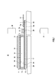
- FIG. 1 is a cross-sectional view showing a process of mounting an IC chip and a flexible substrate on a glass substrate by a mounting apparatus to which the connection method according to the present invention is applied.
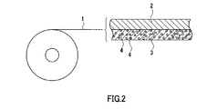
- FIG. 2 is a cross-sectional view showing an anisotropic conductive film.
- connection method a connection body manufacturing method, and a connection body to which the present invention is applied will be described in detail with reference to the drawings. It should be noted that the present invention is not limited to the following embodiments, and various modifications can be made without departing from the scope of the present invention.
- the liquid crystal display panel 10 includes two transparent substrates 11 and 12 made of a glass substrate and the like, and the transparent substrates 11 and 12 are bonded to each other by a frame-shaped seal 13. .
- the liquid crystal 14 is sealed in a space surrounded by the transparent substrates 11 and 12 to form a panel display unit 15.
- the transparent substrates 11 and 12 have a pair of striped transparent electrodes 16 and 17 made of ITO (indium tin oxide) or the like on both inner surfaces facing each other so as to intersect each other.
- the transparent electrodes 16 and 17 are configured such that a pixel as a minimum unit of liquid crystal display is configured by the intersection of the transparent electrodes 16 and 17.
- one transparent substrate 12 is formed to have a larger planar dimension than the other transparent substrate 11, and a liquid crystal driving edge is formed on the edge 12a of the formed transparent substrate 12.
- a COG mounting unit 20 on which an electronic component 18 such as an IC is mounted is provided, and an FOG mounting unit 22 on which a flexible substrate 21 on which a liquid crystal driving circuit is formed is mounted near the outside of the COG mounting unit 20. ing.
- liquid crystal driving IC and the liquid crystal driving circuit can perform predetermined liquid crystal display by selectively changing the alignment of the liquid crystal by selectively applying the liquid crystal driving voltage to the pixels. ing.
- the terminal portions 17a of the transparent electrodes 17 are formed on the mounting portions 20 and 22, respectively.
- an electronic component 18 such as a liquid crystal driving IC and a flexible substrate 21 are connected using the anisotropic conductive film 1 as a conductive adhesive.
- the anisotropic conductive film 1 contains the conductive particles 4, and conducts the electrode of the electronic component 18 or the flexible substrate 21 and the terminal portion 17 a of the transparent electrode 17 formed on the edge portion 12 a of the transparent substrate 12. Electrically connected through the conductive particles 4.
- This anisotropic conductive film 1 is an ultraviolet curable adhesive and a thermosetting adhesive, and is thermally bonded by a heating and pressing head 30 to be described later and irradiated with ultraviolet rays by an ultraviolet irradiator 31, thereby forming conductive particles. 4 is cured in a state where it is crushed between the terminal portion 17a and each electrode of the electronic component or the flexible substrate 21, and the transparent substrate 12, the electronic component 18 and the flexible substrate 21 are connected.
- an alignment film 24 subjected to a predetermined rubbing process is formed on both the transparent electrodes 16 and 17, and the initial alignment of liquid crystal molecules is regulated by the alignment film 24.
- a pair of polarizing plates 25 and 26 are disposed outside the transparent substrates 11 and 12, and these polarizing plates 25 and 26 allow transmitted light from a light source (not shown) such as a backlight to be transmitted. The vibration direction is regulated.
- the anisotropic conductive film 1 is usually one in which a conductive particle-containing layer 3 is formed on a release film 2 serving as a base material. As shown in FIG. 1, the anisotropic conductive film 1 has a conductive particle-containing layer 3 interposed between a transparent electrode 17 formed on a transparent substrate 12 of the liquid crystal display panel 10 and an electronic component 18 or a flexible substrate 21. By doing so, the liquid crystal display panel 10 and the electronic component 18 or the flexible substrate 21 are connected and used for electrical connection.
- a substrate such as a polyethylene terephthalate film generally used in anisotropic conductive films (ACF) can be used.
- the conductive particle-containing layer 3 is formed by dispersing conductive particles 4 in a binder.
- the binder contains a film-forming resin, a curable resin, a curing agent, a silane coupling agent, and the like, and is the same as the binder used for a normal anisotropic conductive film.
- the film forming resin is preferably a resin having an average molecular weight of about 10,000 to 80,000.
- the film forming resin include various resins such as a phenoxy resin, an epoxy resin, a modified epoxy resin, and a urethane resin.
- phenoxy resin is particularly preferable from the viewpoint of film formation state, connection reliability, and the like.
- the curable resin is not particularly limited, and examples thereof include an epoxy resin and an acrylic resin.
- an epoxy resin there is no restriction
- naphthalene type epoxy resin, biphenyl type epoxy resin, phenol novolac type epoxy resin, bisphenol type epoxy resin, stilbene type epoxy resin, triphenolmethane type epoxy resin, phenol aralkyl type epoxy resin, naphthol type epoxy resin, A dicyclopentadiene type epoxy resin, a triphenylmethane type epoxy resin, etc. are mentioned. These may be used alone or in combination of two or more.
- an acrylic resin there is no restriction
- the curing agent is not particularly limited and may be appropriately selected depending on the purpose. However, when the curable resin is an epoxy resin, a cationic curing agent is preferable, and when the curable resin is an acrylic resin, radical curing is performed. Agents are preferred.
- curing agent there is no restriction
- curing agent For example, a sulfonium salt, onium salt, etc. can be mentioned, Among these, an aromatic sulfonium salt is preferable.
- curing agent According to the objective, it can select suitably, For example, an organic peroxide can be mentioned.
- silane coupling agents include epoxy, amino, mercapto sulfide, ureido and the like. By adding the silane coupling agent, the adhesion at the interface between the organic material and the inorganic material is improved.
- Examples of the conductive particles 4 include any known conductive particles used in anisotropic conductive films.
- Examples of the conductive particles 4 include particles of various metals and metal alloys such as nickel, iron, copper, aluminum, tin, lead, chromium, cobalt, silver, gold, metal oxide, carbon, graphite, glass, ceramic, Examples thereof include those in which the surface of particles such as plastic is coated with metal, or those in which the surface of these particles is further coated with an insulating thin film.
- examples of the resin particle include an epoxy resin, a phenol resin, an acrylic resin, an acrylonitrile / styrene (AS) resin, a benzoguanamine resin, a divinylbenzene resin, a styrene resin, and the like. Can be mentioned.
- the anisotropic conductive film 1 is temporarily pressure-bonded onto the transparent electrode 17.
- the method of temporarily press-bonding the anisotropic conductive film 1 is performed such that the conductive particle-containing layer 3 is on the transparent electrode 17 side on the transparent electrode 17 of the transparent substrate 12 of the liquid crystal display panel 10. Place.
- the electroconductive particle content layer 3 is heated and pressurized by the heating press head 30, for example from the peeling film 2 side, and the heating press head 30 is peeled from the peeling film 2.
- the heating press head 30 is peeled from the peeling film 2.
- Temporary pressure bonding by the heating and pressing head 30 heats the upper surface of the release film 2 while pressing it against the transparent electrode 17 side with a slight pressure (for example, about 0.1 MPa to 2 MPa).
- the heating temperature is set to such a temperature that the thermosetting resin such as epoxy resin or acrylic resin in the anisotropic conductive film 1 is not cured (for example, about 70 to 100 ° C.).
- the electronic component 18 is arranged so that the transparent electrode 17 of the transparent substrate 12 and the electrode terminal of the electronic component 18 face each other with the conductive particle-containing layer 3 interposed therebetween.
- the heat pressing temperature by the heating and pressing head 30 is a temperature of ⁇ 10 to 20 ° C. (for example, 120 ° C.) with respect to a predetermined temperature indicating a viscosity (minimum melt viscosity) when the conductive particle-containing layer 3 is melted before the start of curing. Around °C). Thereby, the warp of the transparent substrate 12 is minimized, and the electronic component 18 is not damaged by heat.
- the anisotropic conductive film 1 is irradiated with ultraviolet rays by the ultraviolet irradiator 31 provided on the back side of the transparent substrate 12.
- the ultraviolet light emitted from the ultraviolet irradiator 31 passes through a transparent support base such as glass that supports the transparent substrate 12 and the transparent substrate 12 supported by the support base, and is irradiated to the conductive particle-containing layer 3.
- a transparent support base such as glass that supports the transparent substrate 12 and the transparent substrate 12 supported by the support base, and is irradiated to the conductive particle-containing layer 3.
- a mercury lamp, a metal halide lamp, an LED lamp, or the like can be used.
- the anisotropic conductive film 1 undergoes a curing reaction due to heat generated by the heating and pressing head 30 and ultraviolet rays from the ultraviolet irradiator 31, whereby the electronic component 18 is placed on the terminal portion 17 a via the anisotropic conductive film 1. Crimped. The thermal pressurization by the heating and pressing head 30 and the ultraviolet irradiation by the ultraviolet irradiator 31 are completed simultaneously or before and after.
- the electronic component 18 is pressed by the heating and pressing head 30, and the ultraviolet irradiator 31 irradiates ultraviolet rays. At this time, the ultraviolet irradiator 31 increases the irradiation amount in stages. Further, in the present technology, it is preferable to irradiate ultraviolet rays after a predetermined time has passed after the electronic component 18 is pressed by the heating and pressing head 30.
- the progress of the curing reaction of the binder resin is delayed at the initial stage of the ultraviolet irradiation, and the curing reaction of the binder resin is rapidly advanced at the later stage of the ultraviolet irradiation. This is because if the illuminance is high from the beginning of the ultraviolet irradiation, the reaction start point of the binder resin becomes too large, resulting in a cured product having a short molecular chain and inferior heat resistance.
- This technology irradiates with a relatively weak illuminance at the beginning of ultraviolet irradiation and increases the illuminance at a later stage, so that it can be made into a cured product with excellent heat resistance, and the connection reliability is improved while lowering the mounting temperature. Can be increased.
- the illuminance of ultraviolet rays is increased in a plurality of stages, and the number of stages can be appropriately set according to the total irradiation amount of ultraviolet rays, the irradiation time, etc., and is preferably set to 2 to 10 stages. .
- the conductive particle-containing layer 3 of the anisotropic conductive film 1 is fluidized, and the transparent electrode 17 of the transparent substrate 12 and the electrode terminal of the electronic component 18
- the binder resin can be caused to flow out from between the conductive particles 4 so as to be sandwiched therebetween.
- further heat pressurization and irradiation with ultraviolet rays are performed so that the conductive particle-containing layer 3 becomes the transparent electrode 17 of the transparent substrate 12 and the electrode terminal of the electronic component 18.
- ultraviolet rays are irradiated after a predetermined time, preferably about 1 to 10 seconds. Moreover, you may press the heating press head 30 continuously or intermittently, while irradiating an ultraviolet-ray.
- the irradiation time by the ultraviolet irradiator 31, the irradiation stage and the irradiation amount, and the total irradiation amount are determined by the binder resin composition and the heat-pressing temperature, pressure and time by the heating and pressing head 30, so that the curing reaction of the binder proceeds most efficiently. Set the conditions.
- a preferable range of the irradiation amount is 500 to 3000 mJ / sec, and a preferable range of the irradiation stage is set to 2 to 10 stages.
- [Final dose] / [First dose] is preferably 4-10.
- the ultraviolet irradiator 31 presses the flexible substrate 21 by the heating and pressing head 30, and irradiates the ultraviolet rays after a predetermined time (for example, about 1 to 10 seconds) has elapsed. Moreover, you may press the heating press head 30 continuously or intermittently, while irradiating an ultraviolet-ray. Further, the ultraviolet irradiator 31 increases the irradiation amount in stages.
- connection body in which the transparent substrate 12 and the electronic component 18 or the flexible substrate 21 are connected via the anisotropic conductive film 1.
- these COG mounting and FOG mounting may be performed collectively by a single thermal pressurization and ultraviolet irradiation.
- the COG mounting in which the liquid crystal driving IC is directly mounted on the glass substrate of the liquid crystal display panel and the FOG mounting in which the flexible substrate is directly mounted on the substrate of the liquid crystal display panel have been described as examples. It can be used for other various connections other than the FOG mounting.
- the glass substrate is likely to warp due to thermal pressurization due to the narrowing of the mounting area on the outer periphery of the glass substrate and the thinning of the glass substrate.
- the liquid crystal screen around the COG mounting area becomes uneven in color. Since the warpage of the glass substrate is caused by the difference in thermal expansion coefficient between the IC chip and the glass substrate, it is required to lower the mounting temperature, but it is also necessary to prevent the connection reliability from being lowered.
- the mounting temperature is lowered only by the minimum heating necessary for melting the anisotropic conductive film without requiring the high-temperature heating required for thermosetting, thereby reducing the warpage of the substrate. Connection reliability can be ensured while preventing.
- the present technology can also use a photocurable conductive adhesive that is cured by light of other wavelengths such as infrared light.
- the anisotropic conductive film 1 having a film shape as a conductive adhesive has been described, but there is no problem even if it is in a paste form.
- a film-like conductive adhesive film such as the anisotropic conductive film 1 containing the conductive particles 4 or a paste-like conductive adhesive paste is defined as “adhesive”.
- a conductive adhesive that is solid at normal temperature and melts when heated is used.
- a conductive adhesive having fluidity at normal temperature may be used.
- heating is not a requirement, and a conductive adhesive is applied to the COG mounting part 20 and the FOG mounting part, and after the electronic component 18 and the flexible substrate 21 are arranged, ultraviolet rays are irradiated while appropriately pressurizing with a predetermined pressure. To establish a connection.
- the ultraviolet irradiation amount is increased by changing the ultraviolet irradiation amount in multiple stages, but the ultraviolet irradiation amount by the ultraviolet irradiator 31 may be increased linearly. Also in this case, the illuminance per irradiation time is set in consideration of the total irradiation amount, and is increased linearly. By using an LED lamp as the ultraviolet irradiator 31, the irradiation time and illuminance can be easily increased in multiple steps or linearly.
- the conductive particle-containing layer is Phenoxy resin (YP-50: manufactured by Nippon Steel Chemical Co., Ltd.); 45 parts by mass epoxy resin (EP-828: manufactured by Mitsubishi Chemical Corporation); 50 parts by mass silane coupling agent (KBM-403: Shin-Etsu Chemical Co., Ltd.) 1 part by weight curing agent (SI-60L: manufactured by Sanshin Chemical Industry Co., Ltd.); 4 parts by weight conductive particles; (AUL 704: manufactured by Sekisui Chemical Co., Ltd.): 50,000 particles / mm2 were mixed with dispersion.
- the resin composition was adjusted to prepare a cationic curing electrode bonding sheet having a thickness of 20 ⁇ m.
- An ITO coating lath having a glass thickness of 0.5 mm was used as an evaluation base material to which an evaluation IC was connected.
- a connected body sample in which the IC for evaluation was connected to the ITO coating lath through a conductive particle-containing layer by heat and pressure and appropriately irradiated with ultraviolet rays was formed.
- the ultraviolet irradiator a UV irradiator ZUV-C30H (manufactured by OMRON Corporation) was used. Further, in each connected body sample subjected to ultraviolet irradiation, the total irradiation amount is 900 mJ, and in a connected body sample having an irradiation time of 3 seconds, the ultraviolet light is irradiated after 1 second from the start of thermal pressurization to the evaluation IC by the heating press head 30.
- the heating temperature of the heating and pressing head is ⁇ ⁇ 40 ° C. with respect to the temperature (120 ° C.) indicating the viscosity (minimum melt viscosity) when the conductive particle-containing layer is melted before the start of curing. Set to the range.
- Example 1 the heating temperature by the heating and pressing head was 120 ° C., the pressure was 60 MPa, and the thermal pressing time was 4 seconds.
- ultraviolet irradiation was performed in two stages for 3 seconds. In the first stage, the UV illumination was 100 mJ for 2 seconds, and in the second stage, the UV illumination was 700 mJ for 1 second.
- Example 2 the heating conditions by the heating press head were the same as in Example 1.
- ultraviolet irradiation was performed in two stages for 3 seconds. In the first stage, the UV illumination was 50 mJ for 2 seconds, and in the second stage, the UV illumination was 800 mJ for 1 second.
- Example 3 the heating conditions by the heating and pressing head were the same as those in Example 1.
- ultraviolet irradiation was performed in two stages for 3 seconds. In the first stage, the UV illumination was 100 mJ for 1 second, and in the second stage, the UV illumination was 400 mJ for 2 seconds.
- Example 4 the heating conditions by the heating and pressing head were the same as in Example 1.
- the ultraviolet irradiation was performed in 3 steps for 3 seconds. In the first stage, the UV illuminance was 100 mJ for 1 second, in the second stage, the UV illuminance was 300 mJ for 1 second, and in the third stage, the UV illuminance was 500 mJ for 1 second.
- Example 5 the heating conditions by the heating and pressing head were the same as those in Example 1.
- the ultraviolet irradiation was performed in two stages for 3 seconds. In the first stage, the UV illumination was 50 mJ for 1 second, and in the second stage, the UV illumination was 425 mJ for 2 seconds.
- Example 6 the heating conditions by the heating and pressing head were the same as in Example 1.
- the ultraviolet irradiation was performed in 3 steps for 3 seconds.
- the UV illumination was 50 mJ for 1 second
- the UV illumination was 300 mJ for 1 second
- the UV illumination was 550 mJ for 1 second.
- Example 7 the heating conditions by the heating and pressing head were the same as those in Example 1. Further, ultraviolet irradiation was performed in 3 stages for 4 seconds, with the first stage being 1 second at a UV illuminance of 50 mJ, the second stage being 2 seconds at a UV illuminance of 200 mJ, and the third stage being 1 second at a UV illuminance of 450 mJ.
- Example 8 the heating conditions by the heating and pressing head were the same as in Example 1.
- ultraviolet irradiation was performed in three stages for 3 seconds, with the first stage being 1 second with a UV illuminance of 100 mJ, the second stage being 1 second with a UV illuminance of 200 mJ, and the third stage being 1 second with a UV illuminance of 600 mJ.
- Example 9 the heating condition by the heating and pressing head was set to 80 ° C., which is ⁇ 40 ° C. from the temperature (120 ° C.) showing the lowest melt viscosity of the binder resin, and the other conditions were the same as in Example 8.
- Example 10 the heating condition by the heating and pressing head was set to 90 ° C., which is ⁇ 30 ° C. from the temperature (120 ° C.) indicating the lowest melt viscosity of the binder resin, and the other conditions were the same as in Example 8.
- Example 11 the heating condition by the heating and pressing head was set to 140 ° C., which is + 20 ° C. from the temperature (120 ° C.) indicating the lowest melt viscosity of the binder resin, and the other conditions were the same as in Example 8.
- Example 12 the heating condition by the heating and pressing head was set to 150 ° C., which is + 30 ° C. from the temperature (120 ° C.) showing the minimum melt viscosity of the binder resin, and the other conditions were the same as in Example 8.
- the heating temperature by the heating and pressing head was 170 ° C.
- the pressure was 60 MPa
- the thermal pressing time was 4 seconds.
- ultraviolet irradiation was not performed.
- Example 2 the heating conditions by the heating and pressing head were the same as those in Example 1. Moreover, ultraviolet irradiation was not performed.
- Example 3 the heating conditions by the heating and pressing head were the same as those in Example 1. Moreover, as UV irradiation conditions, it was set as 3 second by UV illumination intensity 300mJ.
- Example 4 the heating conditions by the heating and pressing head were the same as those in Example 1.
- ultraviolet irradiation was performed in two stages for 3 seconds. In the first stage, UV illumination was 200 mJ for 2 seconds, and in the second stage, UV illumination was 500 mJ for 1 second.
- Example 5 the heating conditions by the heating and pressing head were the same as those in Example 1.
- ultraviolet irradiation was performed in two stages for 3 seconds. In the first stage, the UV illumination was 150 mJ for 2 seconds, and in the second stage, the UV illumination was 600 mJ for 1 second.
- Example 6 the heating conditions by the heating and pressing head were the same as those in Example 1.
- ultraviolet irradiation was performed in two stages for 3 seconds. In the first stage, UV illumination was 200 mJ for 1 second, and in the second stage, UV illumination was 350 mJ for 2 seconds.
- Example 7 the heating conditions by the heating and pressing head were the same as those in Example 1.
- the ultraviolet irradiation was performed in two stages for 3 seconds. In the first stage, the UV illumination was 150 mJ for 1 second, and in the second stage, the UV illumination was 375 mJ for 2 seconds.
- connection body sample of the above Example and the comparative example the reaction rate (%) of the electroconductive particle content layer was measured by measuring the reduction
- connection resistance at the time of flowing 2 mA of electric currents with the 4-terminal method was measured using the digital multimeter.
- each connected body sample was scanned from the bottom surface of the ITO coating lath of the evaluation substrate using a stylus type surface roughness meter (SE-3H: manufactured by Kosaka Laboratory Ltd.), and the ITO after connection of the evaluation IC was connected The amount of warp ( ⁇ m) of the glass surface of the coating lath was measured. The measurement results are shown in Tables 1 and 2.
- the reaction rate was 95% or more in all connected body samples except Comparative Example 2. This is because in Examples 1 to 12 and Comparative Examples 3 to 7, the heat pressure conditions (80 ° C. to 150 ° C., 60 MPa, 4 seconds) and the ultraviolet irradiation conditions (900 mJ, 3 seconds or 4 seconds), and in Comparative Example 1, the heat and pressure conditions (170 ° C., 60 MPa, 4 seconds) were set so that the reaction rate was 90% or more only by heat and pressure. It depends on the setting.
- Comparative Example 2 the reaction rate was as low as 41% because ultraviolet irradiation was not performed under the same heat and pressure conditions as in Examples 1 to 8 set on the premise of combined use of ultraviolet irradiation. For this reason, in Comparative Example 2, the initial conduction resistance value was as high as 1.8 ( ⁇ ), and the conduction resistance value after the high temperature and high humidity test exceeded 100 ( ⁇ ).
- the conductive particle-containing layer showed a reaction rate of 91% or more, the initial conduction resistance value was 0.2 ( ⁇ ), and the conduction after the high-temperature and high-humidity test. The resistance value was as low as 9.6 ( ⁇ ) or less.
- the heat pressing temperature by the heating press head can be kept low at 80 ° C. to 150 ° C. by using ultraviolet irradiation together, and the warp of the glass substrate is 12.4 ( ⁇ m) or less. I was able to suppress it.
- the warp of the glass substrate was 16 .2 ( ⁇ m).
- the UV illuminance in the first stage of UV irradiation is less than about 17% (about 150 mJ / sec) of the total irradiation amount (900 mJ) under predetermined ultraviolet irradiation conditions (900 mJ, 3 seconds, or 4 seconds in this embodiment). It can be seen that irradiation with an illuminance of less than
- the irradiation time by UV illuminance in the first stage of UV irradiation is about 20 to about 20 to the total irradiation time (3 seconds or 4 seconds) under predetermined ultraviolet irradiation conditions (900 mJ, 3 seconds or 4 seconds in this embodiment). It can be seen that about 40% (about 1 second to 2 seconds) is preferable.
- Example 9 Comparing Example 8 to Example 12 with respect to the heating conditions with the heating and pressing head, in Example 9, the heating temperature was as low as ⁇ 40 ° C. with respect to the temperature at which the binder resin exhibits the lowest melt viscosity (120 ° C.). Therefore, the fluidity of the resin was poor compared to other examples, and the binder resin could not be sufficiently removed from between the terminals. Therefore, the conduction resistance value after the high temperature and high humidity test was relatively 9.6 ( ⁇ ). It became high.
- Example 11 when the heating temperature is increased with respect to the temperature (120 ° C.) at which the binder resin exhibits the lowest melt viscosity, the warpage of the substrate becomes larger than in other examples.
- the heating conditions by the heating and pressing head can be used in the range of ⁇ 40 ° C. to + 30 ° C. (80 ° C. to 150 ° C.) with respect to the temperature at which the binder resin exhibits the minimum melt viscosity (120 ° C.). It can be seen that the binder resin is preferably used in a range up to about ⁇ 30 ° C. (around 90 ° C. to 120 ° C.) with respect to the temperature (120 ° C.) at which the minimum melt viscosity is exhibited.
Landscapes
- Engineering & Computer Science (AREA)
- Manufacturing & Machinery (AREA)
- Microelectronics & Electronic Packaging (AREA)
- Wire Bonding (AREA)
- Adhesives Or Adhesive Processes (AREA)
- Combinations Of Printed Boards (AREA)
- Electric Connection Of Electric Components To Printed Circuits (AREA)
Abstract
Selon l'invention, une fiabilité de connexion est garantie, tandis que la température de montage est abaissée. Le procédé de connexion de l'invention comporte une étape au cours de laquelle un objet de connexion et un objet à connecter sont collés par l'intermédiaire d'un adhésif de type photodurcissable, l'adhésif est durci par exposition de ce dernier à une lumière, et l'objet de connexion et l'objet à connecter sont ainsi connectés. L'intensité de la lumière est élevée de manière continue ou graduelle.
Priority Applications (3)
| Application Number | Priority Date | Filing Date | Title |
|---|---|---|---|
| HK14106971.4A HK1193693B (en) | 2011-06-06 | 2012-06-05 | Connection method, connected-body production method and connected body |
| CN201280027638.3A CN103563497B (zh) | 2011-06-06 | 2012-06-05 | 连接方法、连接体的制造方法以及连接体 |
| KR1020137034948A KR101517323B1 (ko) | 2011-06-06 | 2012-06-05 | 접속 방법, 접속체의 제조 방법, 접속체 |
Applications Claiming Priority (2)
| Application Number | Priority Date | Filing Date | Title |
|---|---|---|---|
| JP2011-126642 | 2011-06-06 | ||
| JP2011126642A JP5745944B2 (ja) | 2011-06-06 | 2011-06-06 | 接続方法、接続体の製造方法、接続体 |
Publications (1)
| Publication Number | Publication Date |
|---|---|
| WO2012169497A1 true WO2012169497A1 (fr) | 2012-12-13 |
Family
ID=47296060
Family Applications (1)
| Application Number | Title | Priority Date | Filing Date |
|---|---|---|---|
| PCT/JP2012/064481 Ceased WO2012169497A1 (fr) | 2011-06-06 | 2012-06-05 | Procédé de connexion, et corps de connexion ainsi que procédé de fabrication de celui-ci |
Country Status (5)
| Country | Link |
|---|---|
| JP (1) | JP5745944B2 (fr) |
| KR (1) | KR101517323B1 (fr) |
| CN (1) | CN103563497B (fr) |
| TW (1) | TWI540591B (fr) |
| WO (1) | WO2012169497A1 (fr) |
Cited By (2)
| Publication number | Priority date | Publication date | Assignee | Title |
|---|---|---|---|---|
| WO2016060098A1 (fr) * | 2014-10-16 | 2016-04-21 | デクセリアルズ株式会社 | Procédé de fabrication de connecteur, procédé de connexion de composant électronique, et connecteur |
| US9887222B2 (en) | 2013-08-21 | 2018-02-06 | Canon Kabushiki Kaisha | Method of manufacturing optical apparatus |
Families Citing this family (6)
| Publication number | Priority date | Publication date | Assignee | Title |
|---|---|---|---|---|
| WO2014111745A2 (fr) * | 2013-01-18 | 2014-07-24 | Daimler Ag | Ensembles pile à combustible et procédés pour les préparer |
| JP6291165B2 (ja) * | 2013-03-15 | 2018-03-14 | デクセリアルズ株式会社 | 接続体の製造方法、及び電子部品の接続方法 |
| JP6221285B2 (ja) * | 2013-03-21 | 2017-11-01 | 日立化成株式会社 | 回路部材の接続方法 |
| US20170229417A1 (en) * | 2014-08-22 | 2017-08-10 | Sharp Kabushiki Kaisha | Mounting substrate manufacturing apparatus and method of manufacturing mounting substrate |
| JP2016064378A (ja) * | 2014-09-25 | 2016-04-28 | 東芝ライテック株式会社 | 光照射装置及び光照射方法 |
| JP6679320B2 (ja) | 2015-01-20 | 2020-04-15 | デクセリアルズ株式会社 | 接続体の製造方法、電子部品の接続方法 |
Citations (4)
| Publication number | Priority date | Publication date | Assignee | Title |
|---|---|---|---|---|
| JP2000349427A (ja) * | 1999-06-07 | 2000-12-15 | Ibiden Co Ltd | プリント配線板、表面実装用プリント配線板及び表面実装配線板 |
| JP2007298608A (ja) * | 2006-04-28 | 2007-11-15 | Victor Co Of Japan Ltd | 光学部品の製造方法 |
| JP2010016388A (ja) * | 2009-07-13 | 2010-01-21 | Hitachi Chem Co Ltd | 回路接続方法 |
| JP2010050238A (ja) * | 2008-08-20 | 2010-03-04 | Seiko Epson Corp | 接合方法および接合体 |
Family Cites Families (2)
| Publication number | Priority date | Publication date | Assignee | Title |
|---|---|---|---|---|
| JP4609350B2 (ja) * | 2006-03-14 | 2011-01-12 | パナソニック株式会社 | 電子部品実装構造体の製造方法 |
| JP2009290231A (ja) * | 2009-09-01 | 2009-12-10 | Hitachi Chem Co Ltd | 回路板装置の製造法 |
-
2011
- 2011-06-06 JP JP2011126642A patent/JP5745944B2/ja active Active
-
2012
- 2012-06-05 WO PCT/JP2012/064481 patent/WO2012169497A1/fr not_active Ceased
- 2012-06-05 KR KR1020137034948A patent/KR101517323B1/ko active Active
- 2012-06-05 CN CN201280027638.3A patent/CN103563497B/zh active Active
- 2012-06-06 TW TW101120197A patent/TWI540591B/zh active
Patent Citations (4)
| Publication number | Priority date | Publication date | Assignee | Title |
|---|---|---|---|---|
| JP2000349427A (ja) * | 1999-06-07 | 2000-12-15 | Ibiden Co Ltd | プリント配線板、表面実装用プリント配線板及び表面実装配線板 |
| JP2007298608A (ja) * | 2006-04-28 | 2007-11-15 | Victor Co Of Japan Ltd | 光学部品の製造方法 |
| JP2010050238A (ja) * | 2008-08-20 | 2010-03-04 | Seiko Epson Corp | 接合方法および接合体 |
| JP2010016388A (ja) * | 2009-07-13 | 2010-01-21 | Hitachi Chem Co Ltd | 回路接続方法 |
Cited By (7)
| Publication number | Priority date | Publication date | Assignee | Title |
|---|---|---|---|---|
| US9887222B2 (en) | 2013-08-21 | 2018-02-06 | Canon Kabushiki Kaisha | Method of manufacturing optical apparatus |
| WO2016060098A1 (fr) * | 2014-10-16 | 2016-04-21 | デクセリアルズ株式会社 | Procédé de fabrication de connecteur, procédé de connexion de composant électronique, et connecteur |
| JP2016082070A (ja) * | 2014-10-16 | 2016-05-16 | デクセリアルズ株式会社 | 接続体の製造方法、電子部品の接続方法、接続体 |
| KR20170069962A (ko) * | 2014-10-16 | 2017-06-21 | 데쿠세리아루즈 가부시키가이샤 | 접속체의 제조 방법, 전자 부품의 접속 방법, 접속체 |
| CN107079589A (zh) * | 2014-10-16 | 2017-08-18 | 迪睿合株式会社 | 连接体的制造方法、电子部件的连接方法、连接体 |
| CN107079589B (zh) * | 2014-10-16 | 2020-06-09 | 迪睿合株式会社 | 连接体的制造方法、电子部件的连接方法、连接体 |
| KR102476432B1 (ko) * | 2014-10-16 | 2022-12-09 | 데쿠세리아루즈 가부시키가이샤 | 접속체의 제조 방법, 전자 부품의 접속 방법, 접속체 |
Also Published As
| Publication number | Publication date |
|---|---|
| CN103563497B (zh) | 2016-08-17 |
| JP2012253282A (ja) | 2012-12-20 |
| KR101517323B1 (ko) | 2015-05-04 |
| TWI540591B (zh) | 2016-07-01 |
| HK1193693A1 (zh) | 2014-09-26 |
| KR20140024935A (ko) | 2014-03-03 |
| CN103563497A (zh) | 2014-02-05 |
| TW201301301A (zh) | 2013-01-01 |
| JP5745944B2 (ja) | 2015-07-08 |
Similar Documents
| Publication | Publication Date | Title |
|---|---|---|
| JP5745944B2 (ja) | 接続方法、接続体の製造方法、接続体 | |
| JP5972844B2 (ja) | 異方性導電フィルム、異方性導電フィルムの製造方法、接続体の製造方法、及び接続方法 | |
| JP6679320B2 (ja) | 接続体の製造方法、電子部品の接続方法 | |
| JP5836830B2 (ja) | 接続体の製造方法、及び接続方法 | |
| JP5926590B2 (ja) | 接続体の製造方法、及び電子部品の接続方法 | |
| JP6317508B2 (ja) | 異方性導電フィルム、異方性導電フィルムの製造方法、接続体の製造方法、及び接続方法 | |
| JP2015142120A (ja) | 接続体の製造方法、電子部品の接続方法及び接続装置 | |
| HK1245501A1 (zh) | 连接体的制造方法 | |
| JP6291165B2 (ja) | 接続体の製造方法、及び電子部品の接続方法 | |
| WO2015111599A1 (fr) | Procédé de production de corps de connexion et procédé de connexion de composant électronique | |
| HK1193693B (en) | Connection method, connected-body production method and connected body | |
| WO2016117613A1 (fr) | Procédé de fabrication de corps connecté, procédé de connexion de composant électronique et corps connecté | |
| JP2015170647A (ja) | 接続体の製造方法、電子部品の接続方法及び接続体 |
Legal Events
| Date | Code | Title | Description |
|---|---|---|---|
| 121 | Ep: the epo has been informed by wipo that ep was designated in this application |
Ref document number: 12796249 Country of ref document: EP Kind code of ref document: A1 |
|
| NENP | Non-entry into the national phase |
Ref country code: DE |
|
| ENP | Entry into the national phase |
Ref document number: 20137034948 Country of ref document: KR Kind code of ref document: A |
|
| 122 | Ep: pct application non-entry in european phase |
Ref document number: 12796249 Country of ref document: EP Kind code of ref document: A1 |