WO2012169511A1 - 電子式内視鏡 - Google Patents
電子式内視鏡 Download PDFInfo
- Publication number
- WO2012169511A1 WO2012169511A1 PCT/JP2012/064522 JP2012064522W WO2012169511A1 WO 2012169511 A1 WO2012169511 A1 WO 2012169511A1 JP 2012064522 W JP2012064522 W JP 2012064522W WO 2012169511 A1 WO2012169511 A1 WO 2012169511A1
- Authority
- WO
- WIPO (PCT)
- Prior art keywords
- electronic endoscope
- substrate
- interface board
- unit
- connector
- Prior art date
- Legal status (The legal status is an assumption and is not a legal conclusion. Google has not performed a legal analysis and makes no representation as to the accuracy of the status listed.)
- Ceased
Links
Images





Classifications
-
- A—HUMAN NECESSITIES
- A61—MEDICAL OR VETERINARY SCIENCE; HYGIENE
- A61B—DIAGNOSIS; SURGERY; IDENTIFICATION
- A61B1/00—Instruments for performing medical examinations of the interior of cavities or tubes of the body by visual or photographical inspection, e.g. endoscopes; Illuminating arrangements therefor
- A61B1/00002—Operational features of endoscopes
- A61B1/00011—Operational features of endoscopes characterised by signal transmission
- A61B1/00018—Operational features of endoscopes characterised by signal transmission using electrical cables
-
- A—HUMAN NECESSITIES
- A61—MEDICAL OR VETERINARY SCIENCE; HYGIENE
- A61B—DIAGNOSIS; SURGERY; IDENTIFICATION
- A61B1/00—Instruments for performing medical examinations of the interior of cavities or tubes of the body by visual or photographical inspection, e.g. endoscopes; Illuminating arrangements therefor
- A61B1/00064—Constructional details of the endoscope body
- A61B1/00105—Constructional details of the endoscope body characterised by modular construction
-
- A—HUMAN NECESSITIES
- A61—MEDICAL OR VETERINARY SCIENCE; HYGIENE
- A61B—DIAGNOSIS; SURGERY; IDENTIFICATION
- A61B1/00—Instruments for performing medical examinations of the interior of cavities or tubes of the body by visual or photographical inspection, e.g. endoscopes; Illuminating arrangements therefor
- A61B1/00112—Connection or coupling means
- A61B1/00121—Connectors, fasteners and adapters, e.g. on the endoscope handle
- A61B1/00124—Connectors, fasteners and adapters, e.g. on the endoscope handle electrical, e.g. electrical plug-and-socket connection
-
- A—HUMAN NECESSITIES
- A61—MEDICAL OR VETERINARY SCIENCE; HYGIENE
- A61B—DIAGNOSIS; SURGERY; IDENTIFICATION
- A61B1/00—Instruments for performing medical examinations of the interior of cavities or tubes of the body by visual or photographical inspection, e.g. endoscopes; Illuminating arrangements therefor
- A61B1/005—Flexible endoscopes
- A61B1/0051—Flexible endoscopes with controlled bending of insertion part
-
- A—HUMAN NECESSITIES
- A61—MEDICAL OR VETERINARY SCIENCE; HYGIENE
- A61B—DIAGNOSIS; SURGERY; IDENTIFICATION
- A61B1/00—Instruments for performing medical examinations of the interior of cavities or tubes of the body by visual or photographical inspection, e.g. endoscopes; Illuminating arrangements therefor
- A61B1/04—Instruments for performing medical examinations of the interior of cavities or tubes of the body by visual or photographical inspection, e.g. endoscopes; Illuminating arrangements therefor combined with photographic or television appliances
- A61B1/05—Instruments for performing medical examinations of the interior of cavities or tubes of the body by visual or photographical inspection, e.g. endoscopes; Illuminating arrangements therefor combined with photographic or television appliances characterised by the image sensor, e.g. camera, being in the distal end portion
Definitions
- the present invention relates to an electronic endoscope using a solid-state imaging device, and more particularly to an electronic endoscope in which an insertion portion and an operation portion that are inserted into a subject are detachable.
- Endoscopes are widely used to observe the inside of a living body such as a human body or an animal, or the inside of various machines or facilities.
- Endoscopes are of the type (fiber scope) that inserts an image fiber inside an observation target such as a living body and optically guides the image of the observation target part to the outside of the observation target (fiber scope).
- An electronic device that inserts a small solid-state imaging device inside the object, converts the image of the observation site into an electrical signal, leads the electrical signal to the outside of the observation object, and observes the image on an external monitor. The thing is mainly used.
- an insertion portion inserted into an observation object is contaminated by blood of a patient or the like. Contaminated inserts are usually reused after cleaning and disinfection.
- electronic endoscopes that can be made removable and disposable can be proposed. (For example, refer to Patent Document 1).
- the present invention has been made in the background as described above, and provides an electronic endoscope capable of reducing the burden on a patient by reducing the diameter of the distal end portion of the insertion portion while making the insertion portion detachable. This is a problem.
- the electronic endoscope of the present invention includes a solid-state imaging device at the tip, a long insertion portion that is inserted into the subject, and an operation portion that is detachably connected to the other end of the insertion portion.
- the operation unit at least a part of a circuit board that generates and outputs an image signal from the RAW data obtained by the solid-state image sensor is arranged, and the RAW data obtained by the solid-state image sensor
- the first electric cable for transmitting the cable is connected to the circuit board by a connector or in the middle of the circuit board.
- the tip of the insertion unit can be reduced in diameter. it can.
- an insertion part can be manufactured more cheaply and it can be set as a preferable form as a disposable insertion part.
- the electrical cable is electrically connected at the same time that the insertion portion is attached to the operation portion, the insertion portion and the operation portion can be more easily attached. Further, since the electric cable can be divided, the degree of freedom in the arrangement of the circuit board can be increased.
- an optical fiber that transmits light from a light source provided on the other end side of the insertion portion and emits the light from the distal end of the insertion portion is incorporated in the insertion portion. Is preferred.
- observation can be performed while irradiating light in front of the distal end of the insertion portion.
- a light emitting element is provided inside a distal end of the insertion portion, and power is supplied to the light emitting element from the circuit board by a second electric cable, and the second electric cable is provided.
- the connector is connected to the circuit board or in the middle of the circuit board, and when the insertion part is attached to and detached from the operation part, it is preferably attached and detached at the connector part.
- the configuration can be simplified, and the electric cable can be divided, so that the circuit board can be freely arranged. The degree can be increased.
- the circuit board includes a first board portion on which an analog / digital conversion circuit for converting RAW data obtained by the solid-state imaging device into a digital data signal is mounted; It can be divided into a second substrate portion on which an image signal generation circuit portion for processing a digital data signal to generate an image signal is mounted.
- the first substrate portion is disposed in the insertion portion and the second substrate portion is disposed in the operation portion.
- the length of the electric cable (transmission path length) can be set relatively long.
- both the first board part and the second board part are arranged in the operation part. You may do it. In that case, it is desirable that the first substrate portion and the second substrate portion are overlapped with an interval so that their plate surfaces are parallel to each other and are connected to each other. Further, the first board part is arranged in the insertion part, the second board part is arranged in the operation part, and the first board part and the second board part are connected by a connector. Preferably it is.
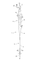
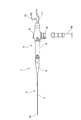
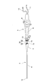
- FIG. 1 is a side view of an electronic endoscope according to an embodiment of the present invention. It is a bottom view of the electronic endoscope of the embodiment of the present invention. 1 is an exploded side view of an electronic endoscope according to an embodiment of the present invention.
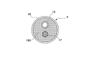
- FIG. 2 is an enlarged cross-sectional view taken along line AA in FIG. It is a B arrow line view of FIG. It is a figure which shows an imaging module. It is a figure which shows a light guide. It is a figure which shows the combination of an imaging module and a light guide. It is an enlarged side view of a tip unit. It is an enlarged view of the connection part of an insertion part and an operation part. It is a schematic diagram which shows an example of the electrical connection structure of an electronic endoscope.
- substrate It is a block diagram which shows an example of a circuit structure at the time of dividing an interface board into two. It is a schematic diagram which shows an example of the electrical connection structure of the electronic endoscope at the time of dividing an interface board into two. It is an enlarged view of an example of the connection part of an insertion part and an operation part at the time of dividing an interface board into two. It is a block diagram which shows another example of a circuit structure at the time of dividing an interface board into two. It is an enlarged view of the other example of the connection part of an insertion part at the time of dividing an interface board into two, and an operation part.
- FIG. 14 is an enlarged view of still another example of the connection portion between the insertion portion and the operation portion when the interface board is divided into two. It is sectional drawing of the insertion part main body of another embodiment. It is sectional drawing of the insertion part main body of another embodiment.
- FIG. 1 is a side view showing the overall configuration of the electronic endoscope 1 of this embodiment
- FIG. 2 is a bottom view.
- an electronic endoscope 1 is provided with a long insertion portion 2 to be inserted into an observation site of a subject and the other end side of the insertion portion.
- the insertion portion 2 includes an insertion portion main body 4 and a bend stopper 5.
- the operation unit 3 includes an operation unit main body 6, an operation lever 8 for bending the vicinity of the distal end of the insertion unit 2, a light guide connection unit 9, and an analog image cable for outputting a captured image to the outside. 10 and a digital image cable 11.
- a light guide 17 (FIGS.
- the insertion portion 2 disposed inside the insertion portion 2 is configured to be connectable to the external light guide 60 via the light guide connection portion 9, and transmits the external light guide 60.
- the transmitted light is introduced into the electronic endoscope 1 when the external light guide 60 is connected to the light guide 17. Further, as described later, by operating the handle 8 to drive the angle wire 44, the vicinity of the distal end of the insertion portion 2 can be bent.
- the electronic endoscope 1 observes an image of a subject imaged by the solid-state imaging device 25 (see FIG. 6) via an objective lens system 26 (see FIG. 6) provided at the distal end portion 16 of the insertion portion 2. Is.
- an objective lens system 26 provided at the distal end portion 16 of the insertion portion 2.
- the insertion portion 2 and the operation portion 3 are detachable. Specifically, it can be detachably connected by the male connection part 14 provided in the bend stopper 5 of the insertion part 2 and the female connection part 15 provided in the operation part main body 6.
- An interface board 13 is built in and fixed inside the operation unit main body 6.
- the insertion part 2 and the operation part 3 are electrically connected by a connector 34. That is, the connector 34 includes a male connector unit 35 provided in the male connection portion 14 and a female connector unit 36 provided in the female connection portion 15, and these connector units 35 and 36 are electrically connected and inserted.
- RAW data obtained by the solid-state imaging device 25 provided at the front end portion 16 of the unit 2 can be transmitted to the interface board 13.
- the RAW data transmitted from the solid-state image sensor 25 is processed by a circuit on the interface board 13.
- the transmission distance of the analog RAW data transmitted from the solid-state imaging device 25 is relatively short (for example, 2 m to 3 m), but is digitized by the interface board 13 in the operation unit body 6 and then retransmitted as an image signal. Can be stretched.
- FIG. 4A is an enlarged cross-sectional view of the insertion portion main body 4.
- a tube in which a first hollow path (lumen) 37A, a second hollow path 37B, and a pair of wire holes 43 are formed in the bowl-shaped insertion portion main body 4 along the longitudinal direction. 18A is provided.
- the insertion section main body 4 is provided with the imaging module 12 inserted through the first hollow path 37A and the light guide 17 inserted through the second hollow path 37B.
- the insertion portion main body 4 is provided with a pair of angle wires 44 inserted through the pair of wire holes 43 and an exterior 45 covering the outermost circumference of the tube 18A over the entire length.
- the angle wire 44 is a wire used for a bending operation in the vicinity of the distal end of the insertion portion 2.
- the operation lever 8 is swung in either direction from the neutral state shown in FIG. 1, and one of the two angle wires 44 is drawn and the other is drawn.
- the tube 18A is preferably a flexible resin.
- a polyacetal resin or a polyimide resin can be used.
- the exterior 45 has a layer structure made of, for example, a SUS spiral, a braid, and a sheath (polyurethane resin or the like).
- FIG. 4B is a view showing the distal end of the insertion portion 2. As shown in FIG. 4B, the objective lens system 26 and the light guide 17 are exposed at the distal end of the insertion portion 2.
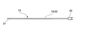
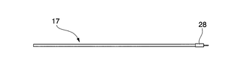
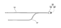
- FIG. 5A to 5C are views showing the imaging module 12 and the light guide 17 housed in the insertion portion main body 4.
- the imaging module 12 includes a tip unit 21 including an objective lens system 26 (see FIG. 6), a solid-state imaging device 25 (see FIG. 6), and a four-core coaxial cable 22 (electric cable).
- the collective coaxial cable 19 is constituted by, for example, a four-core collective coaxial cable formed by collecting four coaxial cables 22.
- the entire assembly of the four coaxial cables 22 is surrounded by a ground conductor layer (shield layer), and the ground conductor layer is further surrounded by a protective coating layer (jacket).
- Each coaxial cable 22 includes, for example, a center conductor, an insulator surrounding the center conductor, an outer conductor surrounding the insulator, and a protective coating layer surrounding the outer conductor.
- the light guide 17 is open at the front end side and irradiated with light, and a male optical connector 28 is provided at the other end side.
- the light guide 17 is formed, for example, by bundling a plurality of plastic optical fibers in a bundle.
- the male connector 23 and the male optical connector 28 can be integrated into a male connector unit 35.
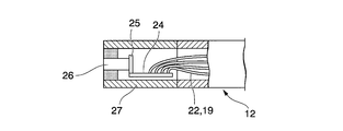
- FIG. 6 is an enlarged side view of the tip unit 21 provided at the tip of the imaging module 12.
- the tip unit 21 includes a cylindrical tip sleeve 27 that forms the outer shape of the tip unit 21, a circuit board 24 provided therein, and a solid attached near the tip of the circuit board 24.
- the imaging device 25 and the objective lens system 26 are provided, and the solid-state imaging device 25 is configured to receive light emitted from the objective lens system 26 and photoelectrically convert an image of the observation target.
- the tip sleeve 27 is made of a hard resin or a metal such as stainless steel.
- the outer diameter of the tip sleeve 27 is, for example, 1.5 mm or less, and more preferably 1.0 mm or less.
- the tip sleeve 27 protects the solid-state imaging device 25 and the like, and the circuit board 24 and the objective lens system 26 are fixed by filling the inside of the tip sleeve 27 with an adhesive resin.
- a coaxial cable 22 for transmitting RAW data output from the solid-state image sensor 25 is connected to the circuit board 24.
- a CMOS image sensor is employed for the solid-state imaging device 25.
- a positive output (AOP) and a negative output (AON) of RAW data of the solid-state imaging device 25 are output from the coaxial cable 22. Further, a clock signal (CLK) and a synchronization signal (HSYNC) are transmitted / received to / from the interface board 13 from the coaxial cable 22. Further, power is supplied from the coaxial cable 22.
- CLK clock signal
- HSELNC synchronization signal
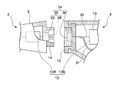
- FIG. 7 is an enlarged view of a connection portion between the insertion portion 2 and the operation portion 3.
- a cylindrical male connection portion 14 is provided at the rear end of the folding stopper 5.
- a male screw is formed on the outer periphery of the male connecting portion 14 and is configured to be connected to a female screw of the female connecting portion 15 described later.
- a male connector unit 35 including a male connector 23 of the imaging module 12 and a male optical connector 28 of the light guide 17 is fixed inside the bend stopper 5.
- the mechanism for connecting the insertion portion 2 and the operation portion 3 is not limited to a mechanism using screws, but it is preferable that the connection can be made without using a special tool or the like.
- the male and female of the connection part and the connector may be reversed.
- a female connection portion 15 is rotatably provided at the front end of the operation portion 3.
- a female screw is formed on the inner periphery of the female connection portion 15 and is configured to be connected to the male connection portion 14 of the insertion portion 2.
- a female connector unit 36 connected to the male connector unit 35 is fitted into the female connection portion 15.
- the female connector unit 36 includes an electrical connection portion connected to the male connector 23 and an optical connection portion connected to the male optical connector 28.
- the female connector unit 36 is electrically connected to the interface board 13 via the collective coaxial cable 30 (first electric cable) and is optically connected to the light guide 31. Similar to the collective coaxial cable 19, the collective coaxial cable 30 is configured by, for example, a four-core collective coaxial cable formed by collecting four coaxial cables 22.
- the male connection portion 14 is provided at the rear end of the insertion portion 2 and the female connection portion 15 is provided at the front end of the operation portion 3. It is detachable. Further, the male connector unit 35 fixed to the male connection portion 14 and the female connector unit 36 fixed to the female connection portion 15 constituting the connector 34 connect the male connection portion 14 and the female connection portion 15 to each other. It is configured to be connected by electricity or light.
- the first electric cable (the collective coaxial cable 19 and the collective coaxial cable 30) is connected to the connector by the connector 34 on the way to the interface board 13, and when the insertion portion 2 is attached to and detached from the operation portion 3.
- the male connector unit 35 and the female connector unit 36 are attached and detached.
- the first electric cable (the collective coaxial cable 19 and the collective coaxial cable 30) is connected to the connector on the way to the interface board 13, but the present invention is not limited to this. That is, for example, the first electric cable (the collective coaxial cable 19 and the collective coaxial cable 30) may be connected to the interface board 13 by a connector. In such an example, for example, the female connector unit 36 is directly attached to the interface board 13.
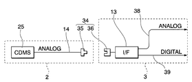
- FIG. 8 is a diagram showing an electrical connection configuration of the electronic endoscope 1 of the present embodiment.
- RAW data is output from the solid-state imaging device 25 of the insertion portion 2, and the interface board 13 is connected via the collective coaxial cable 19 and the male connector unit 35 and the female connector unit 36 that constitute the connector 34. Is input.
- the interface board 13 is for processing the RAW data obtained by the solid-state image sensor 25, generating an image signal, and outputting it. That is, RAW data input to the interface board 13 is converted into an analog image signal 38 and a digital image signal 39.
- the analog image signal 38 is directly connected to a monitor, for example.
- the digital image signal 39 is connected to, for example, a personal computer.
- the image signal generated by the interface board 13 is not limited to both the analog image signal 38 and the digital image signal 39, and may be either the analog image signal 38 or the digital image signal 39.
- FIG. 9 is a configuration diagram of the interface board 13.
- the interface board 13 includes a clock synchronization circuit including a clock generation circuit 51 and a crystal oscillator 52, an analog / digital conversion circuit 53, a signal processing device 54, an image format converter 55, and an NTSC encoding.
- a circuit 56, an NTSC driver circuit 57, a USB driver circuit 58, and a power supply circuit 59 are included.
- the differential signal obtained from the positive output AOP and the negative output AON of the RAW data output from the solid-state imaging device 25 is digitized by the analog / digital conversion circuit 53.
- the digitized differential signal is processed by the signal processing device 54, and as a result, a digital image signal is generated.
- This digital image signal is converted into a digital image signal such as YUV by an image format converter 55.
- the digital image signal from the image format converter 55 is converted into an NTSC-compliant composite image signal by the NTSC encoding circuit 56, and output to a monitor (video image display device) (not shown) by the NTSC driver circuit 57.
- the digital image signal from the image format converter 55 is output from the USB driver circuit 58 to, for example, a personal computer (not shown).
- the interface circuit that digitizes the RAW data and generates the image signal is arranged in the operation unit 3 without being arranged in the insertion unit 2, and the insertion unit 2 has a compact configuration. As a result, the burden on the patient can be reduced. Further, since it is not necessary to arrange an interface circuit for digitizing RAW data and generating an image signal in the insertion portion 2, the insertion portion 2 can be manufactured at a lower cost and is preferable as a disposable insertion portion.
- tip part 16 is built in the insertion part 2, it observes, irradiating light in front of the front-end
- the interface board 13 is configured as a single board and is arranged in the operation unit 3. However, depending on the function of the circuit, the interface board 13 may be divided into two board parts (described later). As described above, the first substrate portion 13A and the second substrate portion 13B may be divided into two parts. Specifically, the interface board 13 includes a first board portion 13A on which an analog / digital conversion circuit 53 for converting RAW data obtained by the solid-state imaging device 25 into a digital data signal is mounted; It can be divided into a second substrate part 13A on which an image signal generation circuit part 61 for processing a data signal and generating an image signal is mounted.
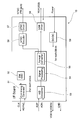
- FIG. 10 shows an example of a specific circuit configuration when the interface board 13 is divided into the first board portion 13A and the second board portion 13B as described above.
- the overall circuit configuration itself composed of the first substrate portion 13A and the second substrate portion 13B is substantially the same as the interface substrate 13 shown in FIG. Is divided into two parts, and one part (a part including the analog / digital conversion circuit 53) is provided on the first substrate part 13A, and the other part (a part including the image signal generation circuit part 61) is provided on the second substrate part. It is mounted on 13B.
- the first substrate unit 13A includes an analog / digital conversion circuit 53 for converting RAW data (analog signal) output from the solid-state imaging device 25 into a digital data signal, a clock generation circuit 51, and A clock synchronization circuit including a crystal oscillator 52 and a first power supply circuit (DC / DC converter; DC voltage conversion circuit) 59A for supplying a power supply voltage to the solid-state imaging device 25 are mounted.
- analog / digital conversion circuit 53 for converting RAW data (analog signal) output from the solid-state imaging device 25 into a digital data signal
- a clock generation circuit 51 for converting A clock synchronization circuit including a crystal oscillator 52 and a first power supply circuit (DC / DC converter; DC voltage conversion circuit) 59A for supplying a power supply voltage to the solid-state imaging device 25 are mounted.
- a digital data signal from the analog / digital conversion circuit 53 of the first substrate unit 13A is processed to generate an image signal (for example, an NTSC signal or a PC digital image signal).
- an image signal generation circuit unit 61 a signal processing device 54, an image format converter 55, an NTSC encoding circuit 56, an NTSC driver circuit 57, and a USB driver circuit 58 are mounted.
- a second power supply circuit (DC / DC converter; DC voltage conversion circuit) 59B for supplying a power supply voltage to each circuit in the circuit portion 61 and the first substrate portion 13A is mounted.
- the first substrate portion 13A is inserted into the insertion portion 2 as shown in FIGS.
- Two substrate parts 13 ⁇ / b> B can be arranged in the operation part 3.
- the first substrate portion 13 ⁇ / b> A is usually disposed in the anti-bending portion 5 in the insertion portion 2.
- the first substrate unit 13A and the second substrate unit 13B are connected by a connector 34. That is, the output side of the first board portion 13A is connected to the male connector unit 35, and the input side of the second board portion 13B is connected to the female connector unit 36.
- the signal passing through the connection portion (male connector unit 35 and female connector unit 36) by the connector 34 has already been A / D converted by the analog / digital conversion circuit 53 of the first board portion 13A. Digital data signal. Therefore, it is possible to avoid an adverse effect due to the collapse or attenuation of the analog waveform at the connector connection portion, such as when an analog signal is passed through the connector connection portion.
- the RAW image data obtained by the solid-state imaging device 25 is an analog signal, not only is the analog waveform distorted or attenuated during transmission through an electric cable, but a connector connection portion is interposed during the transmission. In this case, the analog waveform is likely to be largely corrupted or attenuated at the connector connection portion. This means that the image cannot be correctly reproduced from the image data obtained by the solid-state imaging device 25.
- the connector connection The length of the electric cable (transmission path length) must be determined in consideration of waveform collapse and attenuation at the portion, and therefore the length of the electric cable (transmission path length) is restricted to be relatively short.
- the interface board 13 is divided and the first board part 13A including the analog / digital conversion circuit 53 is arranged in the insertion part 2, the signal passing through the connection part by the connector 34 is already present. Since it is digitized, it is possible to minimize the adverse effects caused by the collapse and attenuation of the signal waveform at the connector connection portion. As a result, the length of the electric cable (transmission path length) can be set relatively long.
- the clock synchronization circuit including the clock generation circuit 51 and the crystal oscillator 52 is mounted on the first substrate portion 13A. It can also be mounted on the part 13B. However, when it is desired to increase the clock speed, it is preferable to mount the clock synchronization circuit on the first substrate portion 13A closer to the solid-state imaging device 25 than the connection portion by the connector 34.
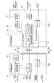
- FIG. 13 shows another example of the circuit configuration when the interface substrate 13 is divided into the first substrate portion 13A and the second substrate portion 13B as described above.
- a defective cell a cell that does not operate or cannot obtain a normal data signal even if it operates
- Defective cell signal cancel circuit 65 for canceling a signal for a defective cell stored in the defective cell memory 63 out of the defective cell memory 63 and the image data signal from the analog / digital conversion circuit 53.
- a signal (digital data signal) at the stage where the signal from the defective cell is canceled is transmitted to the second substrate portion 13A through the defective cell signal cancel circuit 65.
- Other circuit configurations are the same as those shown in FIG.
- the defective cell memory 63 and the defective cell signal cancel circuit 65 are allowed to be mounted on the second substrate unit 13B.
- the defective cell to be stored in the defective cell memory 63 is a specific solid. Since it is associated with the image pickup device 25, as shown in FIG. 13, if the defective cell memory 63 and the defective cell signal cancel circuit 65 are mounted on the first substrate portion 13A disposed in the insertion portion 2, they are mounted. This is convenient when the insertion portion 2 including the solid-state imaging device 25 is replaced.
- the solid-state imaging element 25 is also replaced accordingly. Therefore, if cell defect information about the solid-state imaging device 25 in the insertion portion 2 is stored in advance in the defective cell memory 63 of the first substrate portion 13A in the insertion portion 2 to be newly attached, the insertion portion.
- the cell defect information about the solid-state image sensor 25 of the new insertion portion 2 can be utilized immediately after the replacement.
- the first board part 13A is inserted into the insertion part. 2 and the second substrate unit 13B is arranged in the operation unit 3, but in some cases, as shown in FIG. 14, the first substrate unit 13A and the second substrate unit It is also allowed to place both of them in the operation unit 3 together with 13B.
- the cable between the first substrate unit 13A and the second substrate unit 13B can be appropriately extended according to the shape, size, internal structure, and the like of the operation unit 3.
- the interface board 13 is divided into two board parts (the first board part 13A and the second board part 13B), and both the first board part 13A and the second board part 13B are separated.
- the plate surfaces are stacked so as to be parallel to each other and are connected with each other by a connector 67. It is desirable to do.
- positioning and support pins 69 are interposed between the first substrate portion 13A and the second substrate portion 13B.
- the structure of the interface board 13 as shown in FIG. 15 or FIG. 16 can be called a “two-story structure”. In such a two-story structure, the entire interface board 13 can be made compact as compared with the case where the interface board 13 is not divided. Therefore, the operation unit 3 that accommodates the interface board 13 can be reduced in size.
- the female connector unit 36 constituting the portion of the connector 34 on the operation unit 3 side is electrically connected to the first board portion 13 ⁇ / b> A via the collective coaxial cable 30 (first electric cable). It is connected.
- the cable 30 drawn from the female connector unit 36 is shown in a state of being directly connected to the first board portion 13A, but the cable 30 is electrically connected to the first board portion 13A by a connector (not shown). You may connect.
- the female connector unit 36 constituting the portion of the connector 34 on the operation unit 3 side is directly attached to the first board portion 13A.
- the male connector unit 35 constituting the portion on the insertion portion 2 side of the connector 34 is directly electrically connected to the female connector unit 36 attached to the first board portion 13A.
- the first substrate portion 13A and the second substrate portion 13B are detachably connected by the connector 67.
- the first substrate portion 13A and the second substrate portion 13B are detachably connected to each other. It is also permissible to fix the substrate portion 13B to each other.
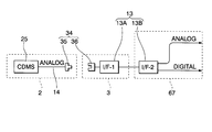
- the interface board 13 is divided into two board parts (first board part 13A and second board part 13B), as shown in FIG. 17, the first board part 13A is operated.
- the second substrate portion 13B is allowed to be disposed in the control box 67 outside the operation portion 3 while being disposed in the portion 3.
- the control box 67 that accommodates the second board portion 13B can be disposed in the vicinity of a monitor (video image display device) or a personal computer (not shown).
- FIG. 18A and FIG. 18B show a cross section of an insertion portion main body according to another embodiment.
- a hollow path 37E is added, and this hollow path 37E is used as a channel. It is a form to use as.
- the channel can be used for a supply path of nutrient solution or medicine. Although not shown, it is assumed that this channel has a mechanism that is attached and detached by attaching and detaching an insertion portion 2 and an operation portion 3 described later.
- the form shown in FIG. 18B is a form in which the wire for the bending operation is eliminated, and is preferably used not for the endoscope but for the catheter tube or the like.
- the means for irradiating light in front of the tip portion 16 is not limited to an optical fiber, and a semiconductor element (LED, light emitting element) that emits light is provided inside the tip portion 16 to replace the optical fiber.
- the power supplied to the LEDs is configured to be supplied from the interface board 13 by the collective coaxial cable 19 (second electric cable).
- the collective coaxial cable 19 is connected to the interface board 13 or in the middle of the interface board 13 by a connector.
- the electric power is configured to be supplied by connecting the male connection unit 14 and the female connection unit 15 and connecting the male connector unit 35 and the female connector unit 36.
- the present invention relates to an electronic endoscope using a solid-state imaging device, and can be applied particularly to an electronic endoscope in which an insertion portion inserted into a subject and an operation portion are detachable.
Landscapes
- Health & Medical Sciences (AREA)
- Life Sciences & Earth Sciences (AREA)
- Surgery (AREA)
- Biomedical Technology (AREA)
- Medical Informatics (AREA)
- Optics & Photonics (AREA)
- Pathology (AREA)
- Radiology & Medical Imaging (AREA)
- Biophysics (AREA)
- Engineering & Computer Science (AREA)
- Physics & Mathematics (AREA)
- Heart & Thoracic Surgery (AREA)
- Nuclear Medicine, Radiotherapy & Molecular Imaging (AREA)
- Molecular Biology (AREA)
- Animal Behavior & Ethology (AREA)
- General Health & Medical Sciences (AREA)
- Public Health (AREA)
- Veterinary Medicine (AREA)
- Endoscopes (AREA)
- Instruments For Viewing The Inside Of Hollow Bodies (AREA)
Abstract
挿入部と操作部とを着脱自在としながら、患者への負担を軽減させることができる電子内視鏡を提供する。そのために、本発明の電子内視鏡は、先端に固体撮像素子を備え、被検体に挿入される長尺状の挿入部と、挿入部の他端に着脱自在に接続される操作部とを備え、操作部の内部には、固体撮像素子によって得られたRAWデータから画像信号を生成して出力するインターフェース基板の少なくとも一部が配置されており、固体撮像素子によって得られたRAWデータを伝送する第1の電気ケーブルは、インターフェース基板に、またはインターフェース基板までの途中でコネクタ接続されており、挿入部を操作部に着脱する際には、コネクタ部分で着脱される構成とした。
Description
本発明は、固体撮像素子を用いた電子式の内視鏡に関し、特に被検体に挿入される挿入部と操作部とが着脱自在とされた電子内視鏡に関する。
本願は、2011年6月6日に、米国に出願された仮出願番号61/493,712に基づき優先権を主張し、その内容をここに援用する。
本願は、2011年6月6日に、米国に出願された仮出願番号61/493,712に基づき優先権を主張し、その内容をここに援用する。
人体や動物などの生体の内部、あるいは各種機械や設備などの内部の状況を観察するために、内視鏡が広く使用されている。内視鏡は、生体などの観察対象物の内部にイメージファイバを挿入して、観察対象部位の画像を観察対象物の外部に光学的に導き出して観察するタイプのもの(ファイバスコープ)と、観察対象物の内部に小型固体撮像素子を挿入し、観察対象部位の画像を電気信号に変換して、その電気信号を観察対象物の外部に導き出し、外部のモニタにより画像を観察する、電子式のものとが主として使用されている。
この種の固体撮像素子からなるイメージセンサを使用した内視鏡における、観察対象物の内部に挿入される挿入部は、使用することによって患者の血液などによって汚染される。汚染された挿入部は、通常は洗浄消毒を経て再利用されるが、近年、洗浄消毒の手間を軽減させるために、挿入部を着脱自在とし、使い捨てとすることができる電子内視鏡が提案されている(例えば、特許文献1参照)。
しかしながら、このような電子内視鏡においては、固体撮像素子を搭載する基板の外形を小さくするのが困難なため、挿入部の先端部の小径化が難しかった。このため、挿入部の先端部が大径化してしまい、患者への負担が少なくなかった。
しかしながら、このような電子内視鏡においては、固体撮像素子を搭載する基板の外形を小さくするのが困難なため、挿入部の先端部の小径化が難しかった。このため、挿入部の先端部が大径化してしまい、患者への負担が少なくなかった。
本発明は、以上のような事情を背景としてなされたもので、挿入部を着脱自在としつつ挿入部の先端部を小径化して患者への負担を軽減させることができる電子内視鏡を提供することを課題とするものである。
したがって本発明の電子内視鏡は、先端に固体撮像素子を備え、被検体に挿入される長尺状の挿入部と、前記挿入部の他端に着脱自在に接続される操作部とを備え、前記操作部の内部には、前記固体撮像素子によって得られたRAWデータから画像信号を生成して出力する回路基板の少なくとも一部が配置されており、前記固体撮像素子によって得られたRAWデータを伝送する第1の電気ケーブルは、前記回路基板にまたは前記回路基板までの途中でコネクタ接続されており、前記挿入部を前記操作部に着脱する際には、コネクタ部分で着脱されることを特徴とする。
上記構成によれば、RAWデータの変換を操作部に配置された回路基板で実行することによって、固体撮像素子に搭載する電気回路を最小限にできるため、挿入部の先端を小径化することができる。また、挿入部に回路基板を配置する必要がないため、挿入部をより安価に製造することができ、使い捨てできる挿入部として好ましい形態とすることができる。
また、挿入部を操作部に装着すると同時に、電気ケーブルの電気的な接続が行われるため、挿入部と操作部との装着をより容易とすることができる。また、電気ケーブルを分割可能としたことにより、回路基板の配置の自由度を高めることができる。
また、挿入部を操作部に装着すると同時に、電気ケーブルの電気的な接続が行われるため、挿入部と操作部との装着をより容易とすることができる。また、電気ケーブルを分割可能としたことにより、回路基板の配置の自由度を高めることができる。
また、前記電子内視鏡において、前記挿入部の内部には、前記挿入部の他端側に設けた光源からの光を伝えて前記挿入部の先端から出射する光ファイバが内蔵されていることが好ましい。
上記構成によれば、観察の際、挿入部の先端前方に光を照射しながら観察することができる。
また、前記電子内視鏡において、前記挿入部の先端の内部には発光素子が設けられ、前記発光素子には第2の電気ケーブルによって前記回路基板から電力が供給され、前記第2の電気ケーブルは、前記回路基板に、または前記回路基板までの途中でコネクタ接続されており、前記挿入部を前記操作部に着脱する際には、コネクタ部分で着脱されることが好ましい。
上記構成によれば、発光素子を発光させるために新たな光源を必要としないため、構成を簡素化することができるとともに、また、電気ケーブルを分割可能としたことにより、回路基板の配置の自由度を高めることができる。
また、前記電子内視鏡において、前記回路基板を、前記固体撮像素子によって得られたRAWデータをデジタルデータ信号に変換するためのアナログ/デジタル変換回路が搭載された第1の基板部と、前記デジタルデータ信号を処理して画像信号を生成するための画像信号生成回路部が搭載された第2の基板部とに分割した構成とすることができる。そしてその場合、前記第1の基板部を前記挿入部内に配置し、前記第2の基板部を前記操作部に配置することが好ましい。
上記構成によれば、コネクタ接続部分を通過する信号は既にデジタル化されているため、コネクタ接続部分における信号波形の崩れや減衰による悪影響を最小限に抑えることができる。またその結果、電気ケーブルの長さ(伝送路長さ)を比較的長く定めることが可能となる。
さらに、上述のように前記回路基板を、第1の基板部と第2の基板部とに分割した構成とした場合、第1の基板部と第2の基板部の両者を前記操作部に配置しても良い。その場合、第1の基板部および第2の基板部が、それらの板面が互いに平行となるように間隔を置いて重ねられるとともに、それらの相互間が連結された構成とすることが望ましい。
さらに、第1の基板部は挿入部内に配置され、第2の基板部は操作部に配置され、第1の基板部と第2の基板部との間がコネクタ接続されるように構成されていることが好ましい。
さらに、第1の基板部は挿入部内に配置され、第2の基板部は操作部に配置され、第1の基板部と第2の基板部との間がコネクタ接続されるように構成されていることが好ましい。
上記構成によれば、第1の基板部と第2の基板部とからなる回路基板の全体をコンパクト化して、それを収容する操作部を小型化することが可能となる。
以下、本発明の実施形態について、図面を参照して詳細に説明する。
図1は、この実施形態の電子内視鏡1の全体構成を示した側面図であり、図2は下面図である。
図1及び図2に示すように、電子内視鏡1は、被検体の観察部位に挿入される長尺状の挿入部2と、この挿入部の他端側に設けられ、電子内視鏡1を把持、操作する為の操作部3とから構成されている。
挿入部2は、挿入部本体4と、折れ止め5とからなる。操作部3は、操作部本体6と、挿入部2の先端付近を屈曲操作するための操作レバー8と、ライトガイド接続部9と、撮像された画像を外部に出力する為の、アナログ画像ケーブル10、デジタル画像ケーブル11とを有する。挿入部2の内部に配置される後述のライトガイド17(図4A、図4B)は、ライトガイド接続部9を介して外部ライトガイド60と接続可能に構成されており、外部ライトガイド60を伝送してきた光は、外部ライトガイド60がライトガイド17に接続されることによって、電子内視鏡1に導入される。また、後述するように、ハンドル8を操作してアングルワイヤ44を駆動させることにより、挿入部2の先端付近は屈曲操作することができる。
図1及び図2に示すように、電子内視鏡1は、被検体の観察部位に挿入される長尺状の挿入部2と、この挿入部の他端側に設けられ、電子内視鏡1を把持、操作する為の操作部3とから構成されている。
挿入部2は、挿入部本体4と、折れ止め5とからなる。操作部3は、操作部本体6と、挿入部2の先端付近を屈曲操作するための操作レバー8と、ライトガイド接続部9と、撮像された画像を外部に出力する為の、アナログ画像ケーブル10、デジタル画像ケーブル11とを有する。挿入部2の内部に配置される後述のライトガイド17(図4A、図4B)は、ライトガイド接続部9を介して外部ライトガイド60と接続可能に構成されており、外部ライトガイド60を伝送してきた光は、外部ライトガイド60がライトガイド17に接続されることによって、電子内視鏡1に導入される。また、後述するように、ハンドル8を操作してアングルワイヤ44を駆動させることにより、挿入部2の先端付近は屈曲操作することができる。
電子内視鏡1は、挿入部2の先端部16に設けられた対物レンズ系26(図6参照)を介して固体撮像素子25(図6参照)によって撮影された被検体の画像を観察するものである。
以下、本実施形態の電子内視鏡1の構造の詳細について述べる。
以下、本実施形態の電子内視鏡1の構造の詳細について述べる。
図3に示すように、本実施形態の電子内視鏡1においては、挿入部2と操作部3とは着脱自在とされている。具体的には、挿入部2の折れ止め5に設けられた雄接続部14と、操作部本体6に設けられた雌接続部15とによって、着脱自在に接続することができる。また、操作部本体6の内部には、インターフェース基板13が内蔵固定されている。
挿入部2と操作部3とはコネクタ34によって電気的に接続されている。すなわちコネクタ34は、雄接続部14に設けられた雄コネクタユニット35と、雌接続部15に設けられた雌コネクタユニット36とからなり、これらのコネクタユニット35、36が電気的に接続され、挿入部2の先端部16に設けられた固体撮像素子25によって得られたRAWデータがインターフェース基板13に送信可能となる。固体撮像素子25から送信されたRAWデータは、インターフェース基板13上の回路によって処理される。
挿入部2と操作部3とはコネクタ34によって電気的に接続されている。すなわちコネクタ34は、雄接続部14に設けられた雄コネクタユニット35と、雌接続部15に設けられた雌コネクタユニット36とからなり、これらのコネクタユニット35、36が電気的に接続され、挿入部2の先端部16に設けられた固体撮像素子25によって得られたRAWデータがインターフェース基板13に送信可能となる。固体撮像素子25から送信されたRAWデータは、インターフェース基板13上の回路によって処理される。
固体撮像素子25から送信されるアナログRAWデータの伝送距離は比較的短いが(例えば2m~3m)、操作部本体6内のインターフェース基板13でデジタル化してから画像信号として再送することで、伝送距離を伸ばすことができる。
図4Aは、挿入部本体4の拡大断面図である。
図4Aに示すように、竿状の挿入部本体4には、長手方向に沿って第一中空路(ルーメン)37A、第二中空路37B、および一対のワイヤ用穴43が形成されているチューブ18Aが設けられている。挿入部本体4には、第一中空路37Aに挿通された撮像モジュール12と、第二中空路37Bに挿通されたライトガイド17が設けられている。挿入部本体4には、一対のワイヤ用穴43に挿通された一対のアングルワイヤ44と、チューブ18A最外周を全長に亘って覆っている外装45とが設けられている。
図4Aに示すように、竿状の挿入部本体4には、長手方向に沿って第一中空路(ルーメン)37A、第二中空路37B、および一対のワイヤ用穴43が形成されているチューブ18Aが設けられている。挿入部本体4には、第一中空路37Aに挿通された撮像モジュール12と、第二中空路37Bに挿通されたライトガイド17が設けられている。挿入部本体4には、一対のワイヤ用穴43に挿通された一対のアングルワイヤ44と、チューブ18A最外周を全長に亘って覆っている外装45とが設けられている。
アングルワイヤ44は、挿入部2の先端近傍の屈曲操作に用いるワイヤである。挿入部2の先端近傍を屈曲させるには、操作レバー8を図1に示す中立状態からいずれかの方向に揺動させ、2本のアングルワイヤ44の一方を繰り寄せると共に、他方を繰り出す。
チューブ18Aは、可撓性を有する樹脂が好ましく、例えばポリアセタール樹脂やポリイミド樹脂を採用することができる。外装45は、例えば、SUSスパイラル、編組、及びシース(ポリウレタン樹脂等)からなる層構造をなしている。
チューブ18Aは、可撓性を有する樹脂が好ましく、例えばポリアセタール樹脂やポリイミド樹脂を採用することができる。外装45は、例えば、SUSスパイラル、編組、及びシース(ポリウレタン樹脂等)からなる層構造をなしている。
図4Bは、挿入部2の先端を示す図である。
図4Bに示すように、挿入部2の先端には、対物レンズ系26と、ライトガイド17が露出されている。
図4Bに示すように、挿入部2の先端には、対物レンズ系26と、ライトガイド17が露出されている。
図5A~図5Cは、挿入部本体4の内部に収納される撮像モジュール12、及びライトガイド17を示す図である。
図5Aに示すように、撮像モジュール12は、対物レンズ系26(図6参照)、固体撮像素子25(図6参照)等を備えた先端ユニット21と、4芯の同軸ケーブル22(電気ケーブル)からなる集合同軸ケーブル19(第1の電気ケーブル)と、雄コネクタ23とを有している。集合同軸ケーブル19は、例えば、4本の同軸ケーブル22を集合してなる4芯集合同軸ケーブルによって構成される。4本の同軸ケーブル22の集合体の全体は、接地導体層(シールド層)によって取り囲まれ、さらにその接地導体層は、保護被覆層(ジャケット)によって取り囲まれている。各同軸ケーブル22は、例えば、中心導体、中心導体を取り囲む絶縁体、絶縁体を取り囲む外部導体、外部導体を取り囲む保護被覆層とからなる。
図5Bに示すように、ライトガイド17は、先端側が開放され光が照射されるようになっているとともに、他端側に雄光コネクタ28が設けられている。ライトガイド17は、例えば複数のプラスチック光ファイバを束状に束ねることによって形成されている。
図5Cに示すように、雄コネクタ23と、雄光コネクタ28とは一体化することによって、雄コネクタユニット35とすることができる。
図5Aに示すように、撮像モジュール12は、対物レンズ系26(図6参照)、固体撮像素子25(図6参照)等を備えた先端ユニット21と、4芯の同軸ケーブル22(電気ケーブル)からなる集合同軸ケーブル19(第1の電気ケーブル)と、雄コネクタ23とを有している。集合同軸ケーブル19は、例えば、4本の同軸ケーブル22を集合してなる4芯集合同軸ケーブルによって構成される。4本の同軸ケーブル22の集合体の全体は、接地導体層(シールド層)によって取り囲まれ、さらにその接地導体層は、保護被覆層(ジャケット)によって取り囲まれている。各同軸ケーブル22は、例えば、中心導体、中心導体を取り囲む絶縁体、絶縁体を取り囲む外部導体、外部導体を取り囲む保護被覆層とからなる。
図5Bに示すように、ライトガイド17は、先端側が開放され光が照射されるようになっているとともに、他端側に雄光コネクタ28が設けられている。ライトガイド17は、例えば複数のプラスチック光ファイバを束状に束ねることによって形成されている。
図5Cに示すように、雄コネクタ23と、雄光コネクタ28とは一体化することによって、雄コネクタユニット35とすることができる。
図6は、撮像モジュール12の先端に設けられた先端ユニット21の拡大側面図である。図6に示すように、先端ユニット21は、先端ユニット21の外形をなす円筒形状の先端スリーブ27と、その内部に設けられた回路基板24と、回路基板24の先端部近傍に取り付けられた固体撮像素子25と、対物レンズ系26とを有し、固体撮像素子25が対物レンズ系26からの出射光を受けて観察対象物の画像を光電変換するよう構成されている。
先端スリーブ27は、硬質の樹脂又はステンレス鋼などの金属からなる。先端スリーブ27の外径は、例えば、1.5mm以下であり、1.0mm以下であることがより好ましい。先端スリーブ27は固体撮像素子25等を保護するものであり、先端スリーブ27の内側に接着樹脂が充填されることによって、回路基板24、対物レンズ系26等を固定している。
回路基板24には、固体撮像素子25から出力されるRAWデータを伝送するための同軸ケーブル22が接続されている。
また、固体撮像素子25にはCMOSイメージセンサが採用されている。回路基板24からは、固体撮像素子25のRAWデータの正出力(AOP)、負出力(AON)が同軸ケーブル22より出力される。また、インターフェース基板13との間でクロック信号(CLK)、同期信号(HSYNC)が同軸ケーブル22より送受信される。また、同軸ケーブル22より電源が供給される。
回路基板24には、固体撮像素子25から出力されるRAWデータを伝送するための同軸ケーブル22が接続されている。
また、固体撮像素子25にはCMOSイメージセンサが採用されている。回路基板24からは、固体撮像素子25のRAWデータの正出力(AOP)、負出力(AON)が同軸ケーブル22より出力される。また、インターフェース基板13との間でクロック信号(CLK)、同期信号(HSYNC)が同軸ケーブル22より送受信される。また、同軸ケーブル22より電源が供給される。
図7は挿入部2と操作部3との接続部の拡大図である。図7に示すように、折れ止め5の後端には、円筒形状の雄接続部14が設けられている。雄接続部14の外周には、雄ねじが形成されており、後述する雌接続部15の雌ねじと接続されるように構成されている。また、折れ止め5の内部には、撮像モジュール12の雄コネクタ23及びライトガイド17の雄光コネクタ28とからなる雄コネクタユニット35が固定されている。
なお、挿入部2と操作部3とを接続するための機構は、ネジによる機構に限ることはないが、特別な工具等を用いることなく接続できることが好ましい。また、接続部やコネクタの雄雌は逆であってもよい。
なお、挿入部2と操作部3とを接続するための機構は、ネジによる機構に限ることはないが、特別な工具等を用いることなく接続できることが好ましい。また、接続部やコネクタの雄雌は逆であってもよい。
操作部3の前端には、雌接続部15が回転自在に設けられている。雌接続部15の内周には雌ねじが形成されており、挿入部2の雄接続部14と接続されるように構成されている。また、雌接続部15には、雄コネクタユニット35と接続される雌コネクタユニット36が嵌め込まれている。雌コネクタユニット36は、雄コネクタ23と接続される電気接続部、及び雄光コネクタ28と接続される光接続部とを備えている。雌コネクタユニット36は集合同軸ケーブル30(第1の電気ケーブル)を介してインターフェース基板13と電気接続されているとともに、ライトガイド31に光接続されている。集合同軸ケーブル30は、集合同軸ケーブル19と同様に、例えば、4本の同軸ケーブル22を集合してなる4芯集合同軸ケーブルによって構成される。
上述したように、挿入部2の後端に雄接続部14が設けられているとともに、操作部3の前端に雌接続部15が設けられていることによって、挿入部2と操作部3とは着脱自在である。また、コネクタ34を構成する、雄接続部14に固定された雄コネクタユニット35および雌接続部15に固定された雌コネクタユニット36は、雄接続部14と雌接続部15とを接続することによって、電気又は光で接続されるように構成されている。
これを言い換えると、第1の電気ケーブル(集合同軸ケーブル19と集合同軸ケーブル30)は、インターフェース基板13までの途中でコネクタ34によりコネクタ接続されており、挿入部2を操作部3に着脱する際には、雄コネクタユニット35および雌コネクタユニット36の部分で着脱される。
なお、この例では、第1の電気ケーブル(集合同軸ケーブル19と集合同軸ケーブル30)は、インターフェース基板13までの途中でコネクタ接続されているが、これに限定される訳ではない。即ち、例えば、第1の電気ケーブル(集合同軸ケーブル19および集合同軸ケーブル30)が、インターフェース基板13にコネクタ接続されていてもよい。このような例では、例えば、雌コネクタユニット36が、インターフェース基板13に直接取り付けられる。
これを言い換えると、第1の電気ケーブル(集合同軸ケーブル19と集合同軸ケーブル30)は、インターフェース基板13までの途中でコネクタ34によりコネクタ接続されており、挿入部2を操作部3に着脱する際には、雄コネクタユニット35および雌コネクタユニット36の部分で着脱される。
なお、この例では、第1の電気ケーブル(集合同軸ケーブル19と集合同軸ケーブル30)は、インターフェース基板13までの途中でコネクタ接続されているが、これに限定される訳ではない。即ち、例えば、第1の電気ケーブル(集合同軸ケーブル19および集合同軸ケーブル30)が、インターフェース基板13にコネクタ接続されていてもよい。このような例では、例えば、雌コネクタユニット36が、インターフェース基板13に直接取り付けられる。
図8は、本実施形態の電子内視鏡1の電気接続構成を示す図である。図8に示すように、挿入部2の固体撮像素子25からはRAWデータが出力され、集合同軸ケーブル19と、コネクタ34を構成する雄コネクタユニット35及び雌コネクタユニット36とを介してインターフェース基板13に入力される。このインターフェース基板13は、前記固体撮像素子25によって得られたRAWデータを処理し、画像信号を生成して出力するためのものである。すなわち、インターフェース基板13に入力されたRAWデータは、アナログ画像信号38と、デジタル画像信号39とに変換される。アナログ画像信号38は、例えば、モニタに直接接続される。デジタル画像信号39は、例えば、パーソナルコンピュータに接続される。なお、インターフェース基板13によって生成される画像信号は、アナログ画像信号38及びデジタル画像信号39の両方に限らず、アナログ画像信号38又はデジタル画像信号39のどちらか一方としてもよい。
図9は、インターフェース基板13の構成図である。図9に示すように、インターフェース基板13は、クロック発生回路51及び水晶発振器52からなるクロック同期回路と、アナログ/デジタル変換回路53と、信号処理装置54と、画像フォーマット変換器55と、NTSCエンコード回路56と、NTSCドライバー回路57と、USBドライバー回路58と、電源回路59とを有する。
以下、画像処理のプロセスについて説明する。
固体撮像素子25から出力されたRAWデータの正出力AOPと負出力AONから得られる差動信号はアナログ/デジタル変換回路53によってデジタル化される。デジタル化された差動信号は、信号処理装置54によって処理され、その結果としてデジタル画像信号が生成される。このデジタル画像信号は、画像フォーマット変換器55によって、例えばYUVといったデジタル画像信号に変換される。
画像フォーマット変換器55からのデジタル画像信号は、NTSCエンコード回路56によってNTSCに準拠したコンポジット画像信号に変換され、NTSCドライバー回路57によって、図示しないモニタ(ビデオ画像表示装置)に向けて出力される。また、画像フォーマット変換器55からのデジタル画像信号は、USBドライバー回路58より、例えば図示しないパーソナルコンピュータに向けて出力される。
固体撮像素子25から出力されたRAWデータの正出力AOPと負出力AONから得られる差動信号はアナログ/デジタル変換回路53によってデジタル化される。デジタル化された差動信号は、信号処理装置54によって処理され、その結果としてデジタル画像信号が生成される。このデジタル画像信号は、画像フォーマット変換器55によって、例えばYUVといったデジタル画像信号に変換される。
画像フォーマット変換器55からのデジタル画像信号は、NTSCエンコード回路56によってNTSCに準拠したコンポジット画像信号に変換され、NTSCドライバー回路57によって、図示しないモニタ(ビデオ画像表示装置)に向けて出力される。また、画像フォーマット変換器55からのデジタル画像信号は、USBドライバー回路58より、例えば図示しないパーソナルコンピュータに向けて出力される。
上記実施形態の電子内視鏡1によれば、RAWデータをデジタル化して画像信号を生成するインターフェース回路を挿入部2に配置せずに操作部3に配置し、挿入部2をコンパクトな構成としたことによって、患者への負担を軽減することができる。また、挿入部2にRAWデータをデジタル化して画像信号を生成するインターフェース回路を配置しなくて済むため、挿入部2をより安価に製造することができ、使い捨てできる挿入部として好ましい。
また、挿入部2は、先端部16の前方に光を照射するためのライトガイド17が内蔵されているため、観察の際、挿入部2の先端部16前方に光を照射しながら観察することができる。
以上の実施形態では、インターフェース基板13を単一の基板としてこれを操作部3内に配置した構成としているが、場合によってはインターフェース基板13を、その回路の機能に応じて二つの基板部(後述するように第1の基板部13Aと第2の基板部13B)に2分割した構成としても良い。
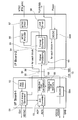
具体的には、インターフェース基板13を、前記固体撮像素子25によって得られたRAWデータをデジタルデータ信号に変換するためのアナログ/デジタル変換回路53が搭載された第1の基板部13Aと、前記デジタルデータ信号を処理して画像信号を生成するための画像信号生成回路部61が搭載された第2の基板部13Aとに分割することができる。このようにインターフェース基板13を第1の基板部13Aと第2の基板部13Bとの分割した場合の具体的回路構成の一例を図10に示す。
具体的には、インターフェース基板13を、前記固体撮像素子25によって得られたRAWデータをデジタルデータ信号に変換するためのアナログ/デジタル変換回路53が搭載された第1の基板部13Aと、前記デジタルデータ信号を処理して画像信号を生成するための画像信号生成回路部61が搭載された第2の基板部13Aとに分割することができる。このようにインターフェース基板13を第1の基板部13Aと第2の基板部13Bとの分割した場合の具体的回路構成の一例を図10に示す。
図10に示す例では、第1の基板部13Aおよび第2の基板部13Bからなる全体的な回路構成自体は、図9に示したインターフェース基板13と実質的に同様であるが、その回路構成の全体を2分割して、一方の部分(アナログ/デジタル変換回路53を含む部分)第1の基板部13Aに、他方の部分(画像信号生成回路部61を含む部分)を第2の基板部13Bに搭載している。
具体的には、第1の基板部13Aには、固体撮像素子25から出力されたRAWデータ(アナログ信号)をデジタルデータ信号に変換するためのアナログ/デジタル変換回路53と、クロック発生回路51及び水晶発振器52からなるクロック同期回路と、前記固体撮像素子25に電源電圧を供給するための第1の電源回路(DC/DCコンバータ;DC電圧変換回路)59Aが搭載されている。
一方第2の基板部13Bには、前記第1の基板部13Aのアナログ/デジタル変換回路53からのデジタルデータ信号を処理して画像信号(例えばNTSC信号やPC用のデジタル画像信号など)を生成するための画像信号生成回路部61として、信号処理装置54と、画像フォーマット変換器55と、NTSCエンコード回路56と、NTSCドライバー回路57と、USBドライバー回路58とが搭載され、さらに前記画像信号生成回路部61および第1の基板部13A内の各回路に電源電圧を供給するための第2の電源回路(DC/DCコンバータ;DC電圧変換回路)59Bとが搭載されている。
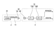
このようにインターフェース基板13を第1の基板部13Aと第2の基板部13Bとの分割した場合、図11、図12に示すように、第1の基板部13Aを挿入部2内に、第2の基板部13Bを操作部3内に配置することができる。ここで、第1の基板部13Aは、図12に示しているように、挿入部2のうちでも、その折れ止め5内に配置するのが通常である。
上述のように第1の基板部13Aを挿入部2内に配置し、第2の基板部13Bを操作部3内に配置した場合、第1の基板部13Aと第2の基板部13Bとの間は、コネクタ34によって接続されている。すなわち、第1の基板部13Aの出力側が雄コネクタユニット35に接続され、第2の基板部13Bの入力側が雌コネクタユニット36に接続されている。
このような構成によれば、コネクタ34による接続部分(雄コネクタユニット35および雌コネクタユニット36)を通過する信号は、既に第1の基板部13Aのアナログ/デジタル変換回路53によってA/D変換されたデジタルデータ信号となっている。そのため、コネクタ接続部分においてアナログ信号を通過させる場合のような、コネクタ接続部分におけるアナログ波形の崩れや減衰による悪影響を回避することができる。
すなわち、固体撮像素子25によって得られたRAW画像データはアナログ信号であるため、電気ケーブルによって伝送される間にアナログ波形の崩れや減衰が生じやすいばかりでなく、その伝送途中にコネクタ接続部分が介在すれば、コネクタ接続部分においてアナログ波形の大きな崩れや大きな減衰が生じやすい。これは、固体撮像素子25によって得られた画像データから、画像を正しく再現できなくなりやすいことを意味する。そのため、アナログ/デジタル変換回路53を含むインターフェース基板13を分割せずに、その全体を操作部3内に配置して、RAW画像データがコネクタ接続部分を通過するように構成した場合は、コネクタ接続部分における波形の崩れや減衰を見込んで電気ケーブルの長さ(伝送路長さ)を定めなければならず、したがって電気ケーブルの長さ(伝送路長さ)が比較的短く制約されてしまう。
これに対して、インターフェース基板13を分割して、アナログ/デジタル変換回路53を含む第1の基板部13Aを挿入部2内に配置しておけば、コネクタ34による接続部分を通過する信号は既にデジタル化されているため、コネクタ接続部分における信号波形の崩れや減衰による悪影響を最小限に抑えることができる。またその結果、電気ケーブルの長さ(伝送路長さ)を比較的長く定めることが可能となる。
なお、図10に示した回路構成では、クロック発生回路51及び水晶発振器52からなるクロック同期回路を第1の基板部13Aに搭載しているが、場合によっては、クロック同期回路を第2の基板部13Bに搭載することも可能である。但し、クロックを高速化したい場合には、クロック同期回路を、コネクタ34による接続部分よりも固体撮像素子25に近い側の第1の基板部13Aに搭載しておくことが好ましい。
前述のようにインターフェース基板13を第1の基板部13Aと第2の基板部13Bとの分割した場合における、回路構成の他の例を図13に示す。
図13に示す例においては、固体撮像素子25における多数のセル(画素)のうち、欠陥のあるセル(作動しないか、または作動しても正常なデータ信号が得られないセル)を予め記憶しておくための欠陥セルメモリ63と、アナログ/デジタル変換回路53からの画像データ信号のうち、前記欠陥セルメモリ63に記憶されている欠陥セルについての信号をキャンセルするための欠陥セル信号キャンセル回路65とが、第1の基板部13Aに搭載されている。そしてこの欠陥セル信号キャンセル回路65を通過して、欠陥セルからの信号がキャンセルされた段階の信号(デジタルデータ信号)が、第2の基板部13Aに送られる。その他の回路構成は、図10に示したものと同様である。
図13に示す例においては、固体撮像素子25における多数のセル(画素)のうち、欠陥のあるセル(作動しないか、または作動しても正常なデータ信号が得られないセル)を予め記憶しておくための欠陥セルメモリ63と、アナログ/デジタル変換回路53からの画像データ信号のうち、前記欠陥セルメモリ63に記憶されている欠陥セルについての信号をキャンセルするための欠陥セル信号キャンセル回路65とが、第1の基板部13Aに搭載されている。そしてこの欠陥セル信号キャンセル回路65を通過して、欠陥セルからの信号がキャンセルされた段階の信号(デジタルデータ信号)が、第2の基板部13Aに送られる。その他の回路構成は、図10に示したものと同様である。
図13に示す回路構成では、固体撮像素子25における欠陥セルからの信号の影響によって画像が正しく再現されなくなるような事態の発生を防止することができる。
なお、欠陥セルメモリ63および欠陥セル信号キャンセル回路65は、第2の基板部13Bに搭載しておくことも許容されるが、欠陥セルメモリ63に記憶させておくべき欠陥セルは、特定の固体撮像素子25に付随するものであるから、図13に示すように、欠陥セルメモリ63および欠陥セル信号キャンセル回路65を挿入部2内に配置される第1の基板部13Aに搭載しておけば、固体撮像素子25を含む挿入部2を交換する場合に好都合となる。
すなわち、挿入部2を前述の接続コネクタ部分で操作部3から分離させて、挿入部2を新たなものに交換する場合には、それに伴って固体撮像素子25も交換されることになる。そこで、新たに取り付けられるべき挿入部2内の第1の基板部13Aの欠陥セルメモリ63に、予めその挿入部2内の固体撮像素子25についてのセル欠陥情報を記憶させておけば、挿入部交換後に直ちに新たな挿入部2の固体撮像素子25についてのセル欠陥情報を活用することができるのである。
なおまた、前述の説明では、インターフェース基板13を二つの基板部分(第1の基板部13Aと第2の基板部13B)に2分割した構成とした場合について、第1の基板部13Aを挿入部2内に配置し、第2の基板部13Bを操作部3内に配置するものとしたが、場合によっては、図14に示しているように、第1の基板部13Aと第2の基板部13Bとの両者を操作部3内に配置することも許容される。この場合、操作部3の形状や寸法、内部構造などに応じて、第1の基板部13Aと第2の基板部13Bとの間のケーブルを適宜延長することができる。
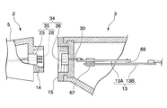
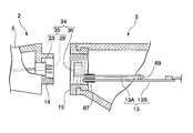
前述のようにインターフェース基板13を二つの基板部分(第1の基板部13Aと第2の基板部13B)に2分割して、第1の基板部13Aと第2の基板部13Bとの両者を操作部3内に配置する場合、例えば図15あるいは図16に示すように、それらの板面が互いに平行となるように間隔を置いて重ねるとともに、それらの相互間をコネクタ67によって連結した構成とすることが望ましい。なお第1の基板部13Aと第2の基板部13Bとの間には、位置決めおよび支持用のピン69が介在している。これらの図15あるいは図16に示すようなインターフェース基板13の構造は、“2階建て構造”ということができる。このような2階建て構造では、インターフェース基板13を分割しない場合と比較して、インターフェース基板13の全体をコンパクト化することができる。そのため、インターフェース基板13を収容する操作部3を小型化することができる。
ここで、図15に示す例では、コネクタ34の操作部3側の部分を構成する雌コネクタユニット36が、集合同軸ケーブル30(第1の電気ケーブル)を介して第1の基板部13Aと電気接続されている。なおここでは、雌コネクタユニット36から引き出されたケーブル30が、第1の基板部13Aに直接接続される状態で示しているが、そのケーブル30を図示しないコネクタによって第1の基板部13Aに電気接続してもよい。
また図16に示す例では、第1の基板部13Aに、コネクタ34の操作部3側の部分を構成する雌コネクタユニット36が直接取り付けられている。この場合、コネクタ34の挿入部2側の部分を構成する雄コネクタユニット35が、第1の基板部13Aに取り付けられた雌コネクタユニット36に直接的に電気接続されることになる。
なお図15、図16に示す各例では、第1の基板部13Aと第2の基板部13Bとがコネクタ67によって着脱可能に接続される構成としているが、第1の基板部13Aと第2の基板部13Bとを相互に固定することも許容される。
さらに、インターフェース基板13を二つの基板部分(第1の基板部13Aと第2の基板部13B)に2分割した場合においては、図17に示しているように、第1の基板部13Aを操作部3内に配置する一方、第2の基板部13Bは、操作部3の外部のコントロールボックス67に配置することも許容される。この場合、第2の基板部13Bを収容したコントロールボックス67は、図示しないモニタ(ビデオ画像表示装置)あるいはパーソナルコンピュータの近傍に配置することができる。
図18A、図18Bは、別の実施形態の挿入部本体の断面を示すものである。一つの別の実施形態としては、図18Aに示すように、集合同軸ケーブル19用の中空路37Cとライトガイド17用の中空路37Dに加え、中空路37Eを追加し、この中空路37Eをチャンネルとして使用する形態である。チャンネルは、栄養液や薬剤などの供給路等に使用することができる。なお、図示しないが、このチャンネルは、後述する挿入部2と操作部3との着脱により着脱する機構を有しているものとする。
また、図18Bに示すように、中空路を2つ形成した上で、一方の中空路37Fにライトガイド40及び集合同軸ケーブル19を挿通させ、もう一方の中空路37Gをチャンネルとして使用する形態としてもよい。また、図18Bに示す形態は、屈曲操作のためのワイヤを廃した形態であり、内視鏡ではなく、カテーテルの管部等に用いることが好ましい。
以上、本発明の好ましい実施形態について説明したが、この実施形態は、あくまで本発明の要旨の範囲内の一つの例に過ぎず、本発明の要旨から逸脱しない範囲内で、構成の付加、省略、置換、およびその他の変更が可能である。本発明は前述した説明によって限定されることはなく、添付のクレームの範囲によってのみ限定される。適宜変更可能であることはもちろんである。
例えば、先端部16の前方に光を照射する手段としては、光ファイバに限ることはなく、発光する半導体素子(LED、発光素子)を先端部16の内部に設けることで光ファイバの代替とすることができる。この場合、LEDに供給される電力は、集合同軸ケーブル19(第2の電気ケーブル)によってインターフェース基板13から供給されるように構成する。また、集合同軸ケーブル19は、インターフェース基板13にまたはインターフェース基板13までの途中でコネクタ接続される。電力は、雄接続部14と雌接続部15とを接続し、雄コネクタユニット35と雌コネクタユニット36とが接続されることによって供給されるように構成されている。
LEDを採用することによって、ライトガイドを配置する必要がなくなり、構成を簡素化することができる。
LEDを採用することによって、ライトガイドを配置する必要がなくなり、構成を簡素化することができる。
固体撮像素子を用いた電子式の内視鏡に関し、特に被検体に挿入される挿入部と操作部とが着脱自在とされた電子内視鏡に適用できる。
1 電子内視鏡
2 挿入部
3 操作部
4 挿入部本体
5 折れ止め
6 本体
8 操作レバー
12 撮像モジュール
13 インターフェース基板
16 先端部
17 ライトガイド
34 コネクタ
45 外装
60 外部ライトガイド
2 挿入部
3 操作部
4 挿入部本体
5 折れ止め
6 本体
8 操作レバー
12 撮像モジュール
13 インターフェース基板
16 先端部
17 ライトガイド
34 コネクタ
45 外装
60 外部ライトガイド
Claims (7)
- 先端に固体撮像素子を備え、被検体に挿入される長尺状の挿入部と、
前記挿入部の他端に着脱自在に接続される操作部と、
前記固体撮像素子によって得られたRAWデータを処理し、画像信号を生成して出力するインターフェース基板とを備え、
前記操作部の内部には、前記インターフェース基板の少なくとも一部が配置されており、
前記固体撮像素子によって得られたRAWデータを伝送する第1の電気ケーブルは、前記インターフェース基板に、または前記インターフェース基板までの途中で、コネクタ接続されており、前記挿入部を前記操作部に着脱する際には、コネクタ部分で着脱されることを特徴とする電子内視鏡。 - 請求項1に記載の電子内視鏡において、
前記挿入部の内部には、前記挿入部の他端側に設けた光源からの光を伝えて前記挿入部の先端から出射する光ファイバが内蔵されていることを特徴とする電子内視鏡。 - 請求項1に記載の電子内視鏡において、
前記挿入部の先端の内部には発光素子が設けられ、前記発光素子には第2の電気ケーブルによって前記インターフェース基板から電力が供給され、前記第2の電気ケーブルは、前記インターフェース基板に、または前記インターフェース基板までの途中でコネクタ接続されており、前記挿入部を前記操作部に着脱する際には、コネクタ部分で着脱されることを特徴とする電子内視鏡。 - 請求項1に記載の電子内視鏡において、
前記インターフェース基板は、前記固体撮像素子によって得られたRAWデータをデジタルデータ信号に変換するためのアナログ/デジタル変換回路が搭載された第1の基板部と、前記デジタルデータ信号を処理して画像信号を生成するための画像信号生成回路部が搭載された第2の基板部とに分割されており、前記第1の基板部と第2の基板部とのうちの少なくとも第2の基板部が前記操作部の内部に配置されていることを特徴とする電子内視鏡。 - 請求項4に記載の電子内視鏡において、
前記第1の基板部および前記第2の基板部が、前記操作部の内部に配置されていることを特徴とする電子内視鏡。 - 請求項5に記載の電子内視鏡において、
前記第1の基板部および前記第2の基板部が、それらの板面が互いに平行となるように間隔を置いて重ねられるとともに、それらの相互間が連結された構成とされていることを特徴とする電子内視鏡。 - 請求項4に記載の電子内視鏡において、
前記第1の基板部は前記挿入部内に配置され、前記第2の基板部は前記操作部に配置され、第1の基板部と第2の基板部との間がコネクタ接続されるように構成されたことを特徴とする電子内視鏡。
Priority Applications (2)
| Application Number | Priority Date | Filing Date | Title |
|---|---|---|---|
| CN201280023711.XA CN103533880A (zh) | 2011-06-06 | 2012-06-06 | 电子式内窥镜 |
| EP12797183.6A EP2689717A4 (en) | 2011-06-06 | 2012-06-06 | ELECTRONIC ENDOSCOPE |
Applications Claiming Priority (2)
| Application Number | Priority Date | Filing Date | Title |
|---|---|---|---|
| US201161493712P | 2011-06-06 | 2011-06-06 | |
| US61/493,712 | 2011-06-06 |
Publications (1)
| Publication Number | Publication Date |
|---|---|
| WO2012169511A1 true WO2012169511A1 (ja) | 2012-12-13 |
Family
ID=47262187
Family Applications (1)
| Application Number | Title | Priority Date | Filing Date |
|---|---|---|---|
| PCT/JP2012/064522 Ceased WO2012169511A1 (ja) | 2011-06-06 | 2012-06-06 | 電子式内視鏡 |
Country Status (5)
| Country | Link |
|---|---|
| US (1) | US20120310045A1 (ja) |
| EP (1) | EP2689717A4 (ja) |
| JP (1) | JPWO2012169511A1 (ja) |
| CN (1) | CN103533880A (ja) |
| WO (1) | WO2012169511A1 (ja) |
Cited By (10)
| Publication number | Priority date | Publication date | Assignee | Title |
|---|---|---|---|---|
| CN103417177A (zh) * | 2013-08-20 | 2013-12-04 | 姜泊 | 一种医用内窥镜插入组件 |
| CN103417178A (zh) * | 2013-08-20 | 2013-12-04 | 姜泊 | 一种一次性医用内窥镜 |
| JP2016504068A (ja) * | 2012-11-22 | 2016-02-12 | ジャイラス・エーシーエムアイ・インコーポレーテッド | 内視鏡カメラヘッドメモリ |
| JP2016077400A (ja) * | 2014-10-14 | 2016-05-16 | パナソニックIpマネジメント株式会社 | 内視鏡 |
| JP2017069600A (ja) * | 2015-09-28 | 2017-04-06 | 株式会社イチワ | 小型カメラ及び撮像装置 |
| CN107080513A (zh) * | 2017-05-17 | 2017-08-22 | 武汉佑康科技有限公司 | 一种模块化内窥镜 |
| JP2019037789A (ja) * | 2018-10-02 | 2019-03-14 | パナソニックIpマネジメント株式会社 | 内視鏡 |
| CN110446450A (zh) * | 2017-03-17 | 2019-11-12 | 国立大学法人大阪大学 | 软性内窥镜和具有该软性内窥镜的内窥镜系统 |
| JP2021087782A (ja) * | 2019-12-04 | 2021-06-10 | ショット アクチエンゲゼルシャフトSchott AG | 内視鏡、使い捨て内視鏡システムおよび内視鏡用の光源 |
| JP2021168841A (ja) * | 2020-04-17 | 2021-10-28 | エア・ウォーター株式会社 | 内視鏡装置及び内視鏡システム |
Families Citing this family (20)
| Publication number | Priority date | Publication date | Assignee | Title |
|---|---|---|---|---|
| JP6180405B2 (ja) | 2011-05-03 | 2017-08-16 | エンドーシー コーポレイションEndosee Corporation | ヒステロスコピー及び子宮内膜生検用の方法及び装置 |
| US9468367B2 (en) | 2012-05-14 | 2016-10-18 | Endosee Corporation | Method and apparatus for hysteroscopy and combined hysteroscopy and endometrial biopsy |
| US9622646B2 (en) | 2012-06-25 | 2017-04-18 | Coopersurgical, Inc. | Low-cost instrument for endoscopically guided operative procedures |
| US9492069B2 (en) * | 2012-07-03 | 2016-11-15 | Covidien Lp | Surgical camera assemblies and systems |
| JP5546597B2 (ja) * | 2012-08-30 | 2014-07-09 | 株式会社フジクラ | 医療機器用ハーネス及び医療機器の組立方法 |
| CN103908213A (zh) * | 2012-12-29 | 2014-07-09 | 上海澳华光电内窥镜有限公司 | 一种脱卸式内视镜装置 |
| JP5748790B2 (ja) * | 2013-02-27 | 2015-07-15 | 富士フイルム株式会社 | 電子内視鏡、及び電子内視鏡の製造方法 |
| US20140275763A1 (en) * | 2013-03-15 | 2014-09-18 | Lucent Medical Systems, Inc. | Partially disposable endoscopic device |
| JP5782064B2 (ja) * | 2013-04-15 | 2015-09-24 | 富士フイルム株式会社 | 内視鏡システム |
| EP3202305B1 (en) * | 2014-09-29 | 2020-07-01 | Dong, Tao | Disposable endoscope and system |
| US10702305B2 (en) | 2016-03-23 | 2020-07-07 | Coopersurgical, Inc. | Operative cannulas and related methods |
| CN110325098A (zh) * | 2016-11-28 | 2019-10-11 | 适内有限责任公司 | 具有可分离一次性轴的内窥镜 |
| US20180228361A1 (en) * | 2017-02-15 | 2018-08-16 | Dynacolor, Inc. | Arthroscopic system with disposable arthroscope |
| US11109747B2 (en) * | 2017-02-15 | 2021-09-07 | Dynacolor, Inc. | Arthroscopic system with disposable arthroscope having image rotation function and method thereof |
| JP6800109B2 (ja) * | 2017-08-22 | 2020-12-16 | オリンパス株式会社 | 超音波内視鏡 |
| KR20250043601A (ko) * | 2018-06-08 | 2025-03-28 | 프리스틴 써지컬 엘엘씨 | 일회용 카메라 샤프트 및 재사용 가능한 손잡이를 갖는 내시경 |
| CN111839435B (zh) * | 2019-04-30 | 2024-09-27 | 新儿护科技医疗器材股份有限公司 | 可更换气管套的内视镜结构 |
| JP7536472B2 (ja) * | 2020-03-03 | 2024-08-20 | Hoya株式会社 | 内視鏡システム |
| JP2024515024A (ja) * | 2021-03-25 | 2024-04-04 | ヘルスケア・コンポーネンツ・グループ | 内視鏡 |
| US20220354357A1 (en) * | 2021-05-06 | 2022-11-10 | The Board Of Regents Of The University Of Texas System | Systems and apparatuses for performing an endoscopy with a detachable insertion cord |
Citations (6)
| Publication number | Priority date | Publication date | Assignee | Title |
|---|---|---|---|---|
| JPH0424018A (ja) * | 1990-05-21 | 1992-01-28 | Fuji Photo Optical Co Ltd | 電子内視鏡 |
| JPH05168591A (ja) * | 1991-12-20 | 1993-07-02 | Fuji Photo Optical Co Ltd | 電子内視鏡用処理ユニットの構造 |
| JPH06254047A (ja) | 1993-03-01 | 1994-09-13 | Olympus Optical Co Ltd | 内視鏡 |
| JP2001061777A (ja) * | 1999-08-26 | 2001-03-13 | Olympus Optical Co Ltd | 電子内視鏡 |
| JP2011036331A (ja) * | 2009-08-07 | 2011-02-24 | Olympus Medical Systems Corp | 電子内視鏡装置 |
| JP2011036414A (ja) * | 2009-08-11 | 2011-02-24 | Hoya Corp | 電子内視鏡および電子内視鏡システム |
Family Cites Families (4)
| Publication number | Priority date | Publication date | Assignee | Title |
|---|---|---|---|---|
| US5609561A (en) * | 1992-06-09 | 1997-03-11 | Olympus Optical Co., Ltd | Electronic type endoscope in which image pickup unit is dismounted to execute disinfection/sterilization processing |
| US6796939B1 (en) * | 1999-08-26 | 2004-09-28 | Olympus Corporation | Electronic endoscope |
| CN100512744C (zh) * | 2004-03-02 | 2009-07-15 | 奥林巴斯株式会社 | 内窥镜 |
| JP2006158859A (ja) * | 2004-12-10 | 2006-06-22 | Olympus Corp | 内視鏡及び内視鏡システム |
-
2012
- 2012-06-01 US US13/486,838 patent/US20120310045A1/en not_active Abandoned
- 2012-06-06 JP JP2013519496A patent/JPWO2012169511A1/ja active Pending
- 2012-06-06 EP EP12797183.6A patent/EP2689717A4/en not_active Withdrawn
- 2012-06-06 CN CN201280023711.XA patent/CN103533880A/zh active Pending
- 2012-06-06 WO PCT/JP2012/064522 patent/WO2012169511A1/ja not_active Ceased
Patent Citations (6)
| Publication number | Priority date | Publication date | Assignee | Title |
|---|---|---|---|---|
| JPH0424018A (ja) * | 1990-05-21 | 1992-01-28 | Fuji Photo Optical Co Ltd | 電子内視鏡 |
| JPH05168591A (ja) * | 1991-12-20 | 1993-07-02 | Fuji Photo Optical Co Ltd | 電子内視鏡用処理ユニットの構造 |
| JPH06254047A (ja) | 1993-03-01 | 1994-09-13 | Olympus Optical Co Ltd | 内視鏡 |
| JP2001061777A (ja) * | 1999-08-26 | 2001-03-13 | Olympus Optical Co Ltd | 電子内視鏡 |
| JP2011036331A (ja) * | 2009-08-07 | 2011-02-24 | Olympus Medical Systems Corp | 電子内視鏡装置 |
| JP2011036414A (ja) * | 2009-08-11 | 2011-02-24 | Hoya Corp | 電子内視鏡および電子内視鏡システム |
Non-Patent Citations (1)
| Title |
|---|
| See also references of EP2689717A4 |
Cited By (14)
| Publication number | Priority date | Publication date | Assignee | Title |
|---|---|---|---|---|
| JP2016504068A (ja) * | 2012-11-22 | 2016-02-12 | ジャイラス・エーシーエムアイ・インコーポレーテッド | 内視鏡カメラヘッドメモリ |
| CN103417177A (zh) * | 2013-08-20 | 2013-12-04 | 姜泊 | 一种医用内窥镜插入组件 |
| CN103417178A (zh) * | 2013-08-20 | 2013-12-04 | 姜泊 | 一种一次性医用内窥镜 |
| CN103417177B (zh) * | 2013-08-20 | 2016-01-27 | 姜泊 | 一种医用内窥镜插入组件 |
| JP2016077400A (ja) * | 2014-10-14 | 2016-05-16 | パナソニックIpマネジメント株式会社 | 内視鏡 |
| US10555664B2 (en) | 2014-10-14 | 2020-02-11 | Panasonic I-Pro Sensing Solutions Co., Ltd. | Endoscope |
| JP2017069600A (ja) * | 2015-09-28 | 2017-04-06 | 株式会社イチワ | 小型カメラ及び撮像装置 |
| CN110446450A (zh) * | 2017-03-17 | 2019-11-12 | 国立大学法人大阪大学 | 软性内窥镜和具有该软性内窥镜的内窥镜系统 |
| CN110446450B (zh) * | 2017-03-17 | 2021-10-01 | 国立大学法人大阪大学 | 软性内窥镜和具有该软性内窥镜的内窥镜系统 |
| CN107080513B (zh) * | 2017-05-17 | 2018-10-16 | 武汉佑康科技有限公司 | 一种模块化内窥镜 |
| CN107080513A (zh) * | 2017-05-17 | 2017-08-22 | 武汉佑康科技有限公司 | 一种模块化内窥镜 |
| JP2019037789A (ja) * | 2018-10-02 | 2019-03-14 | パナソニックIpマネジメント株式会社 | 内視鏡 |
| JP2021087782A (ja) * | 2019-12-04 | 2021-06-10 | ショット アクチエンゲゼルシャフトSchott AG | 内視鏡、使い捨て内視鏡システムおよび内視鏡用の光源 |
| JP2021168841A (ja) * | 2020-04-17 | 2021-10-28 | エア・ウォーター株式会社 | 内視鏡装置及び内視鏡システム |
Also Published As
| Publication number | Publication date |
|---|---|
| CN103533880A (zh) | 2014-01-22 |
| JPWO2012169511A1 (ja) | 2015-02-23 |
| EP2689717A4 (en) | 2014-09-17 |
| EP2689717A1 (en) | 2014-01-29 |
| US20120310045A1 (en) | 2012-12-06 |
Similar Documents
| Publication | Publication Date | Title |
|---|---|---|
| WO2012169511A1 (ja) | 電子式内視鏡 | |
| JP5308716B2 (ja) | 電子内視鏡装置 | |
| US9247867B2 (en) | Endoscopic arrangement | |
| JP5857047B2 (ja) | 電子式内視鏡の撮像部構造 | |
| US8235887B2 (en) | Endoscope assembly with retroscope | |
| CN110151098A (zh) | 视野偏离中心方向的内窥镜系统 | |
| EP1986541A2 (en) | Endoscope | |
| WO2015163942A1 (en) | Integrated medical imaging system | |
| US10687696B2 (en) | Endoscope system with communication mode stabilizing unit | |
| CN114652355A (zh) | 超声波内窥镜 | |
| WO2018155066A1 (ja) | 内視鏡 | |
| CN102946786B (zh) | 激光视频内窥镜 | |
| WO2023019830A1 (zh) | 一种一体化成像组件、内窥镜及回收方法 | |
| JP2010005148A (ja) | 内視鏡及び内視鏡の信号伝送方法 | |
| WO2014188787A1 (ja) | 内視鏡先端構造および内視鏡 | |
| JP5513169B2 (ja) | 内視鏡 | |
| JPWO2015194460A1 (ja) | ケーブル接続構造および内視鏡装置 | |
| CN105007803B (zh) | 摄像单元 | |
| JP2011177263A (ja) | 内視鏡 | |
| JP7759868B2 (ja) | 医療用観察システムおよび伝送ケーブル | |
| JP6744118B2 (ja) | 内視鏡 | |
| JP2009183380A (ja) | 検診用内視鏡 | |
| JP2005288085A (ja) | カプセル内視鏡 | |
| JP2008093454A (ja) | 内視鏡装置 | |
| JP2009165623A (ja) | 検診用内視鏡 |
Legal Events
| Date | Code | Title | Description |
|---|---|---|---|
| 121 | Ep: the epo has been informed by wipo that ep was designated in this application |
Ref document number: 12797183 Country of ref document: EP Kind code of ref document: A1 |
|
| ENP | Entry into the national phase |
Ref document number: 2013519496 Country of ref document: JP Kind code of ref document: A |
|
| WWE | Wipo information: entry into national phase |
Ref document number: 2012797183 Country of ref document: EP |
|
| NENP | Non-entry into the national phase |
Ref country code: DE |