WO2012169511A1 - Endoscope électronique - Google Patents
Endoscope électronique Download PDFInfo
- Publication number
- WO2012169511A1 WO2012169511A1 PCT/JP2012/064522 JP2012064522W WO2012169511A1 WO 2012169511 A1 WO2012169511 A1 WO 2012169511A1 JP 2012064522 W JP2012064522 W JP 2012064522W WO 2012169511 A1 WO2012169511 A1 WO 2012169511A1
- Authority
- WO
- WIPO (PCT)
- Prior art keywords
- electronic endoscope
- substrate
- interface board
- unit
- connector
- Prior art date
- Legal status (The legal status is an assumption and is not a legal conclusion. Google has not performed a legal analysis and makes no representation as to the accuracy of the status listed.)
- Ceased
Links
Images





Classifications
-
- A—HUMAN NECESSITIES
- A61—MEDICAL OR VETERINARY SCIENCE; HYGIENE
- A61B—DIAGNOSIS; SURGERY; IDENTIFICATION
- A61B1/00—Instruments for performing medical examinations of the interior of cavities or tubes of the body by visual or photographical inspection, e.g. endoscopes; Illuminating arrangements therefor
- A61B1/00002—Operational features of endoscopes
- A61B1/00011—Operational features of endoscopes characterised by signal transmission
- A61B1/00018—Operational features of endoscopes characterised by signal transmission using electrical cables
-
- A—HUMAN NECESSITIES
- A61—MEDICAL OR VETERINARY SCIENCE; HYGIENE
- A61B—DIAGNOSIS; SURGERY; IDENTIFICATION
- A61B1/00—Instruments for performing medical examinations of the interior of cavities or tubes of the body by visual or photographical inspection, e.g. endoscopes; Illuminating arrangements therefor
- A61B1/00064—Constructional details of the endoscope body
- A61B1/00105—Constructional details of the endoscope body characterised by modular construction
-
- A—HUMAN NECESSITIES
- A61—MEDICAL OR VETERINARY SCIENCE; HYGIENE
- A61B—DIAGNOSIS; SURGERY; IDENTIFICATION
- A61B1/00—Instruments for performing medical examinations of the interior of cavities or tubes of the body by visual or photographical inspection, e.g. endoscopes; Illuminating arrangements therefor
- A61B1/00112—Connection or coupling means
- A61B1/00121—Connectors, fasteners and adapters, e.g. on the endoscope handle
- A61B1/00124—Connectors, fasteners and adapters, e.g. on the endoscope handle electrical, e.g. electrical plug-and-socket connection
-
- A—HUMAN NECESSITIES
- A61—MEDICAL OR VETERINARY SCIENCE; HYGIENE
- A61B—DIAGNOSIS; SURGERY; IDENTIFICATION
- A61B1/00—Instruments for performing medical examinations of the interior of cavities or tubes of the body by visual or photographical inspection, e.g. endoscopes; Illuminating arrangements therefor
- A61B1/005—Flexible endoscopes
- A61B1/0051—Flexible endoscopes with controlled bending of insertion part
-
- A—HUMAN NECESSITIES
- A61—MEDICAL OR VETERINARY SCIENCE; HYGIENE
- A61B—DIAGNOSIS; SURGERY; IDENTIFICATION
- A61B1/00—Instruments for performing medical examinations of the interior of cavities or tubes of the body by visual or photographical inspection, e.g. endoscopes; Illuminating arrangements therefor
- A61B1/04—Instruments for performing medical examinations of the interior of cavities or tubes of the body by visual or photographical inspection, e.g. endoscopes; Illuminating arrangements therefor combined with photographic or television appliances
- A61B1/05—Instruments for performing medical examinations of the interior of cavities or tubes of the body by visual or photographical inspection, e.g. endoscopes; Illuminating arrangements therefor combined with photographic or television appliances characterised by the image sensor, e.g. camera, being in the distal end portion
Definitions
- the present invention relates to an electronic endoscope using a solid-state imaging device, and more particularly to an electronic endoscope in which an insertion portion and an operation portion that are inserted into a subject are detachable.
- Endoscopes are widely used to observe the inside of a living body such as a human body or an animal, or the inside of various machines or facilities.
- Endoscopes are of the type (fiber scope) that inserts an image fiber inside an observation target such as a living body and optically guides the image of the observation target part to the outside of the observation target (fiber scope).
- An electronic device that inserts a small solid-state imaging device inside the object, converts the image of the observation site into an electrical signal, leads the electrical signal to the outside of the observation object, and observes the image on an external monitor. The thing is mainly used.
- an insertion portion inserted into an observation object is contaminated by blood of a patient or the like. Contaminated inserts are usually reused after cleaning and disinfection.
- electronic endoscopes that can be made removable and disposable can be proposed. (For example, refer to Patent Document 1).
- the present invention has been made in the background as described above, and provides an electronic endoscope capable of reducing the burden on a patient by reducing the diameter of the distal end portion of the insertion portion while making the insertion portion detachable. This is a problem.
- the electronic endoscope of the present invention includes a solid-state imaging device at the tip, a long insertion portion that is inserted into the subject, and an operation portion that is detachably connected to the other end of the insertion portion.
- the operation unit at least a part of a circuit board that generates and outputs an image signal from the RAW data obtained by the solid-state image sensor is arranged, and the RAW data obtained by the solid-state image sensor
- the first electric cable for transmitting the cable is connected to the circuit board by a connector or in the middle of the circuit board.
- the tip of the insertion unit can be reduced in diameter. it can.
- an insertion part can be manufactured more cheaply and it can be set as a preferable form as a disposable insertion part.
- the electrical cable is electrically connected at the same time that the insertion portion is attached to the operation portion, the insertion portion and the operation portion can be more easily attached. Further, since the electric cable can be divided, the degree of freedom in the arrangement of the circuit board can be increased.
- an optical fiber that transmits light from a light source provided on the other end side of the insertion portion and emits the light from the distal end of the insertion portion is incorporated in the insertion portion. Is preferred.
- observation can be performed while irradiating light in front of the distal end of the insertion portion.
- a light emitting element is provided inside a distal end of the insertion portion, and power is supplied to the light emitting element from the circuit board by a second electric cable, and the second electric cable is provided.
- the connector is connected to the circuit board or in the middle of the circuit board, and when the insertion part is attached to and detached from the operation part, it is preferably attached and detached at the connector part.
- the configuration can be simplified, and the electric cable can be divided, so that the circuit board can be freely arranged. The degree can be increased.
- the circuit board includes a first board portion on which an analog / digital conversion circuit for converting RAW data obtained by the solid-state imaging device into a digital data signal is mounted; It can be divided into a second substrate portion on which an image signal generation circuit portion for processing a digital data signal to generate an image signal is mounted.
- the first substrate portion is disposed in the insertion portion and the second substrate portion is disposed in the operation portion.
- the length of the electric cable (transmission path length) can be set relatively long.
- both the first board part and the second board part are arranged in the operation part. You may do it. In that case, it is desirable that the first substrate portion and the second substrate portion are overlapped with an interval so that their plate surfaces are parallel to each other and are connected to each other. Further, the first board part is arranged in the insertion part, the second board part is arranged in the operation part, and the first board part and the second board part are connected by a connector. Preferably it is.
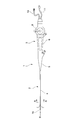
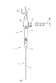
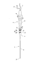
- FIG. 1 is a side view of an electronic endoscope according to an embodiment of the present invention. It is a bottom view of the electronic endoscope of the embodiment of the present invention. 1 is an exploded side view of an electronic endoscope according to an embodiment of the present invention.
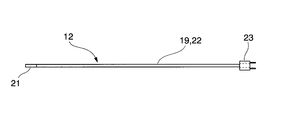
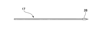
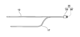
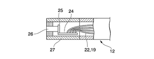
- FIG. 2 is an enlarged cross-sectional view taken along line AA in FIG. It is a B arrow line view of FIG. It is a figure which shows an imaging module. It is a figure which shows a light guide. It is a figure which shows the combination of an imaging module and a light guide. It is an enlarged side view of a tip unit. It is an enlarged view of the connection part of an insertion part and an operation part. It is a schematic diagram which shows an example of the electrical connection structure of an electronic endoscope.
- substrate It is a block diagram which shows an example of a circuit structure at the time of dividing an interface board into two. It is a schematic diagram which shows an example of the electrical connection structure of the electronic endoscope at the time of dividing an interface board into two. It is an enlarged view of an example of the connection part of an insertion part and an operation part at the time of dividing an interface board into two. It is a block diagram which shows another example of a circuit structure at the time of dividing an interface board into two. It is an enlarged view of the other example of the connection part of an insertion part at the time of dividing an interface board into two, and an operation part.
- FIG. 14 is an enlarged view of still another example of the connection portion between the insertion portion and the operation portion when the interface board is divided into two. It is sectional drawing of the insertion part main body of another embodiment. It is sectional drawing of the insertion part main body of another embodiment.
- FIG. 1 is a side view showing the overall configuration of the electronic endoscope 1 of this embodiment
- FIG. 2 is a bottom view.
- an electronic endoscope 1 is provided with a long insertion portion 2 to be inserted into an observation site of a subject and the other end side of the insertion portion.
- the insertion portion 2 includes an insertion portion main body 4 and a bend stopper 5.
- the operation unit 3 includes an operation unit main body 6, an operation lever 8 for bending the vicinity of the distal end of the insertion unit 2, a light guide connection unit 9, and an analog image cable for outputting a captured image to the outside. 10 and a digital image cable 11.
- a light guide 17 (FIGS.
- the insertion portion 2 disposed inside the insertion portion 2 is configured to be connectable to the external light guide 60 via the light guide connection portion 9, and transmits the external light guide 60.
- the transmitted light is introduced into the electronic endoscope 1 when the external light guide 60 is connected to the light guide 17. Further, as described later, by operating the handle 8 to drive the angle wire 44, the vicinity of the distal end of the insertion portion 2 can be bent.
- the electronic endoscope 1 observes an image of a subject imaged by the solid-state imaging device 25 (see FIG. 6) via an objective lens system 26 (see FIG. 6) provided at the distal end portion 16 of the insertion portion 2. Is.
- an objective lens system 26 provided at the distal end portion 16 of the insertion portion 2.
- the insertion portion 2 and the operation portion 3 are detachable. Specifically, it can be detachably connected by the male connection part 14 provided in the bend stopper 5 of the insertion part 2 and the female connection part 15 provided in the operation part main body 6.
- An interface board 13 is built in and fixed inside the operation unit main body 6.
- the insertion part 2 and the operation part 3 are electrically connected by a connector 34. That is, the connector 34 includes a male connector unit 35 provided in the male connection portion 14 and a female connector unit 36 provided in the female connection portion 15, and these connector units 35 and 36 are electrically connected and inserted.
- RAW data obtained by the solid-state imaging device 25 provided at the front end portion 16 of the unit 2 can be transmitted to the interface board 13.
- the RAW data transmitted from the solid-state image sensor 25 is processed by a circuit on the interface board 13.
- the transmission distance of the analog RAW data transmitted from the solid-state imaging device 25 is relatively short (for example, 2 m to 3 m), but is digitized by the interface board 13 in the operation unit body 6 and then retransmitted as an image signal. Can be stretched.
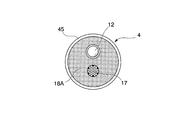
- FIG. 4A is an enlarged cross-sectional view of the insertion portion main body 4.
- a tube in which a first hollow path (lumen) 37A, a second hollow path 37B, and a pair of wire holes 43 are formed in the bowl-shaped insertion portion main body 4 along the longitudinal direction. 18A is provided.
- the insertion section main body 4 is provided with the imaging module 12 inserted through the first hollow path 37A and the light guide 17 inserted through the second hollow path 37B.
- the insertion portion main body 4 is provided with a pair of angle wires 44 inserted through the pair of wire holes 43 and an exterior 45 covering the outermost circumference of the tube 18A over the entire length.
- the angle wire 44 is a wire used for a bending operation in the vicinity of the distal end of the insertion portion 2.
- the operation lever 8 is swung in either direction from the neutral state shown in FIG. 1, and one of the two angle wires 44 is drawn and the other is drawn.
- the tube 18A is preferably a flexible resin.
- a polyacetal resin or a polyimide resin can be used.
- the exterior 45 has a layer structure made of, for example, a SUS spiral, a braid, and a sheath (polyurethane resin or the like).
- FIG. 4B is a view showing the distal end of the insertion portion 2. As shown in FIG. 4B, the objective lens system 26 and the light guide 17 are exposed at the distal end of the insertion portion 2.
- FIG. 5A to 5C are views showing the imaging module 12 and the light guide 17 housed in the insertion portion main body 4.
- the imaging module 12 includes a tip unit 21 including an objective lens system 26 (see FIG. 6), a solid-state imaging device 25 (see FIG. 6), and a four-core coaxial cable 22 (electric cable).
- the collective coaxial cable 19 is constituted by, for example, a four-core collective coaxial cable formed by collecting four coaxial cables 22.
- the entire assembly of the four coaxial cables 22 is surrounded by a ground conductor layer (shield layer), and the ground conductor layer is further surrounded by a protective coating layer (jacket).
- Each coaxial cable 22 includes, for example, a center conductor, an insulator surrounding the center conductor, an outer conductor surrounding the insulator, and a protective coating layer surrounding the outer conductor.
- the light guide 17 is open at the front end side and irradiated with light, and a male optical connector 28 is provided at the other end side.
- the light guide 17 is formed, for example, by bundling a plurality of plastic optical fibers in a bundle.
- the male connector 23 and the male optical connector 28 can be integrated into a male connector unit 35.
- FIG. 6 is an enlarged side view of the tip unit 21 provided at the tip of the imaging module 12.
- the tip unit 21 includes a cylindrical tip sleeve 27 that forms the outer shape of the tip unit 21, a circuit board 24 provided therein, and a solid attached near the tip of the circuit board 24.
- the imaging device 25 and the objective lens system 26 are provided, and the solid-state imaging device 25 is configured to receive light emitted from the objective lens system 26 and photoelectrically convert an image of the observation target.
- the tip sleeve 27 is made of a hard resin or a metal such as stainless steel.
- the outer diameter of the tip sleeve 27 is, for example, 1.5 mm or less, and more preferably 1.0 mm or less.
- the tip sleeve 27 protects the solid-state imaging device 25 and the like, and the circuit board 24 and the objective lens system 26 are fixed by filling the inside of the tip sleeve 27 with an adhesive resin.
- a coaxial cable 22 for transmitting RAW data output from the solid-state image sensor 25 is connected to the circuit board 24.
- a CMOS image sensor is employed for the solid-state imaging device 25.
- a positive output (AOP) and a negative output (AON) of RAW data of the solid-state imaging device 25 are output from the coaxial cable 22. Further, a clock signal (CLK) and a synchronization signal (HSYNC) are transmitted / received to / from the interface board 13 from the coaxial cable 22. Further, power is supplied from the coaxial cable 22.
- CLK clock signal
- HSELNC synchronization signal
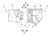
- FIG. 7 is an enlarged view of a connection portion between the insertion portion 2 and the operation portion 3.
- a cylindrical male connection portion 14 is provided at the rear end of the folding stopper 5.
- a male screw is formed on the outer periphery of the male connecting portion 14 and is configured to be connected to a female screw of the female connecting portion 15 described later.
- a male connector unit 35 including a male connector 23 of the imaging module 12 and a male optical connector 28 of the light guide 17 is fixed inside the bend stopper 5.
- the mechanism for connecting the insertion portion 2 and the operation portion 3 is not limited to a mechanism using screws, but it is preferable that the connection can be made without using a special tool or the like.
- the male and female of the connection part and the connector may be reversed.
- a female connection portion 15 is rotatably provided at the front end of the operation portion 3.
- a female screw is formed on the inner periphery of the female connection portion 15 and is configured to be connected to the male connection portion 14 of the insertion portion 2.
- a female connector unit 36 connected to the male connector unit 35 is fitted into the female connection portion 15.
- the female connector unit 36 includes an electrical connection portion connected to the male connector 23 and an optical connection portion connected to the male optical connector 28.
- the female connector unit 36 is electrically connected to the interface board 13 via the collective coaxial cable 30 (first electric cable) and is optically connected to the light guide 31. Similar to the collective coaxial cable 19, the collective coaxial cable 30 is configured by, for example, a four-core collective coaxial cable formed by collecting four coaxial cables 22.
- the male connection portion 14 is provided at the rear end of the insertion portion 2 and the female connection portion 15 is provided at the front end of the operation portion 3. It is detachable. Further, the male connector unit 35 fixed to the male connection portion 14 and the female connector unit 36 fixed to the female connection portion 15 constituting the connector 34 connect the male connection portion 14 and the female connection portion 15 to each other. It is configured to be connected by electricity or light.
- the first electric cable (the collective coaxial cable 19 and the collective coaxial cable 30) is connected to the connector by the connector 34 on the way to the interface board 13, and when the insertion portion 2 is attached to and detached from the operation portion 3.
- the male connector unit 35 and the female connector unit 36 are attached and detached.
- the first electric cable (the collective coaxial cable 19 and the collective coaxial cable 30) is connected to the connector on the way to the interface board 13, but the present invention is not limited to this. That is, for example, the first electric cable (the collective coaxial cable 19 and the collective coaxial cable 30) may be connected to the interface board 13 by a connector. In such an example, for example, the female connector unit 36 is directly attached to the interface board 13.
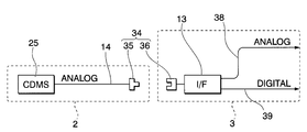
- FIG. 8 is a diagram showing an electrical connection configuration of the electronic endoscope 1 of the present embodiment.
- RAW data is output from the solid-state imaging device 25 of the insertion portion 2, and the interface board 13 is connected via the collective coaxial cable 19 and the male connector unit 35 and the female connector unit 36 that constitute the connector 34. Is input.
- the interface board 13 is for processing the RAW data obtained by the solid-state image sensor 25, generating an image signal, and outputting it. That is, RAW data input to the interface board 13 is converted into an analog image signal 38 and a digital image signal 39.
- the analog image signal 38 is directly connected to a monitor, for example.
- the digital image signal 39 is connected to, for example, a personal computer.
- the image signal generated by the interface board 13 is not limited to both the analog image signal 38 and the digital image signal 39, and may be either the analog image signal 38 or the digital image signal 39.
- FIG. 9 is a configuration diagram of the interface board 13.
- the interface board 13 includes a clock synchronization circuit including a clock generation circuit 51 and a crystal oscillator 52, an analog / digital conversion circuit 53, a signal processing device 54, an image format converter 55, and an NTSC encoding.
- a circuit 56, an NTSC driver circuit 57, a USB driver circuit 58, and a power supply circuit 59 are included.
- the differential signal obtained from the positive output AOP and the negative output AON of the RAW data output from the solid-state imaging device 25 is digitized by the analog / digital conversion circuit 53.
- the digitized differential signal is processed by the signal processing device 54, and as a result, a digital image signal is generated.
- This digital image signal is converted into a digital image signal such as YUV by an image format converter 55.
- the digital image signal from the image format converter 55 is converted into an NTSC-compliant composite image signal by the NTSC encoding circuit 56, and output to a monitor (video image display device) (not shown) by the NTSC driver circuit 57.
- the digital image signal from the image format converter 55 is output from the USB driver circuit 58 to, for example, a personal computer (not shown).
- the interface circuit that digitizes the RAW data and generates the image signal is arranged in the operation unit 3 without being arranged in the insertion unit 2, and the insertion unit 2 has a compact configuration. As a result, the burden on the patient can be reduced. Further, since it is not necessary to arrange an interface circuit for digitizing RAW data and generating an image signal in the insertion portion 2, the insertion portion 2 can be manufactured at a lower cost and is preferable as a disposable insertion portion.
- tip part 16 is built in the insertion part 2, it observes, irradiating light in front of the front-end
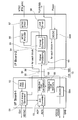
- the interface board 13 is configured as a single board and is arranged in the operation unit 3. However, depending on the function of the circuit, the interface board 13 may be divided into two board parts (described later). As described above, the first substrate portion 13A and the second substrate portion 13B may be divided into two parts. Specifically, the interface board 13 includes a first board portion 13A on which an analog / digital conversion circuit 53 for converting RAW data obtained by the solid-state imaging device 25 into a digital data signal is mounted; It can be divided into a second substrate part 13A on which an image signal generation circuit part 61 for processing a data signal and generating an image signal is mounted.
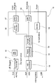
- FIG. 10 shows an example of a specific circuit configuration when the interface board 13 is divided into the first board portion 13A and the second board portion 13B as described above.
- the overall circuit configuration itself composed of the first substrate portion 13A and the second substrate portion 13B is substantially the same as the interface substrate 13 shown in FIG. Is divided into two parts, and one part (a part including the analog / digital conversion circuit 53) is provided on the first substrate part 13A, and the other part (a part including the image signal generation circuit part 61) is provided on the second substrate part. It is mounted on 13B.
- the first substrate unit 13A includes an analog / digital conversion circuit 53 for converting RAW data (analog signal) output from the solid-state imaging device 25 into a digital data signal, a clock generation circuit 51, and A clock synchronization circuit including a crystal oscillator 52 and a first power supply circuit (DC / DC converter; DC voltage conversion circuit) 59A for supplying a power supply voltage to the solid-state imaging device 25 are mounted.
- analog / digital conversion circuit 53 for converting RAW data (analog signal) output from the solid-state imaging device 25 into a digital data signal
- a clock generation circuit 51 for converting A clock synchronization circuit including a crystal oscillator 52 and a first power supply circuit (DC / DC converter; DC voltage conversion circuit) 59A for supplying a power supply voltage to the solid-state imaging device 25 are mounted.
- a digital data signal from the analog / digital conversion circuit 53 of the first substrate unit 13A is processed to generate an image signal (for example, an NTSC signal or a PC digital image signal).
- an image signal generation circuit unit 61 a signal processing device 54, an image format converter 55, an NTSC encoding circuit 56, an NTSC driver circuit 57, and a USB driver circuit 58 are mounted.
- a second power supply circuit (DC / DC converter; DC voltage conversion circuit) 59B for supplying a power supply voltage to each circuit in the circuit portion 61 and the first substrate portion 13A is mounted.
- the first substrate portion 13A is inserted into the insertion portion 2 as shown in FIGS.
- Two substrate parts 13 ⁇ / b> B can be arranged in the operation part 3.
- the first substrate portion 13 ⁇ / b> A is usually disposed in the anti-bending portion 5 in the insertion portion 2.
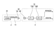
- the first substrate unit 13A and the second substrate unit 13B are connected by a connector 34. That is, the output side of the first board portion 13A is connected to the male connector unit 35, and the input side of the second board portion 13B is connected to the female connector unit 36.
- the signal passing through the connection portion (male connector unit 35 and female connector unit 36) by the connector 34 has already been A / D converted by the analog / digital conversion circuit 53 of the first board portion 13A. Digital data signal. Therefore, it is possible to avoid an adverse effect due to the collapse or attenuation of the analog waveform at the connector connection portion, such as when an analog signal is passed through the connector connection portion.
- the RAW image data obtained by the solid-state imaging device 25 is an analog signal, not only is the analog waveform distorted or attenuated during transmission through an electric cable, but a connector connection portion is interposed during the transmission. In this case, the analog waveform is likely to be largely corrupted or attenuated at the connector connection portion. This means that the image cannot be correctly reproduced from the image data obtained by the solid-state imaging device 25.
- the connector connection The length of the electric cable (transmission path length) must be determined in consideration of waveform collapse and attenuation at the portion, and therefore the length of the electric cable (transmission path length) is restricted to be relatively short.
- the interface board 13 is divided and the first board part 13A including the analog / digital conversion circuit 53 is arranged in the insertion part 2, the signal passing through the connection part by the connector 34 is already present. Since it is digitized, it is possible to minimize the adverse effects caused by the collapse and attenuation of the signal waveform at the connector connection portion. As a result, the length of the electric cable (transmission path length) can be set relatively long.
- the clock synchronization circuit including the clock generation circuit 51 and the crystal oscillator 52 is mounted on the first substrate portion 13A. It can also be mounted on the part 13B. However, when it is desired to increase the clock speed, it is preferable to mount the clock synchronization circuit on the first substrate portion 13A closer to the solid-state imaging device 25 than the connection portion by the connector 34.
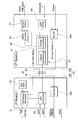
- FIG. 13 shows another example of the circuit configuration when the interface substrate 13 is divided into the first substrate portion 13A and the second substrate portion 13B as described above.
- a defective cell a cell that does not operate or cannot obtain a normal data signal even if it operates
- Defective cell signal cancel circuit 65 for canceling a signal for a defective cell stored in the defective cell memory 63 out of the defective cell memory 63 and the image data signal from the analog / digital conversion circuit 53.
- a signal (digital data signal) at the stage where the signal from the defective cell is canceled is transmitted to the second substrate portion 13A through the defective cell signal cancel circuit 65.
- Other circuit configurations are the same as those shown in FIG.
- the defective cell memory 63 and the defective cell signal cancel circuit 65 are allowed to be mounted on the second substrate unit 13B.
- the defective cell to be stored in the defective cell memory 63 is a specific solid. Since it is associated with the image pickup device 25, as shown in FIG. 13, if the defective cell memory 63 and the defective cell signal cancel circuit 65 are mounted on the first substrate portion 13A disposed in the insertion portion 2, they are mounted. This is convenient when the insertion portion 2 including the solid-state imaging device 25 is replaced.
- the solid-state imaging element 25 is also replaced accordingly. Therefore, if cell defect information about the solid-state imaging device 25 in the insertion portion 2 is stored in advance in the defective cell memory 63 of the first substrate portion 13A in the insertion portion 2 to be newly attached, the insertion portion.
- the cell defect information about the solid-state image sensor 25 of the new insertion portion 2 can be utilized immediately after the replacement.
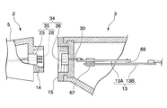
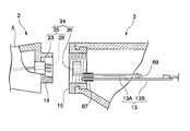
- the first board part 13A is inserted into the insertion part. 2 and the second substrate unit 13B is arranged in the operation unit 3, but in some cases, as shown in FIG. 14, the first substrate unit 13A and the second substrate unit It is also allowed to place both of them in the operation unit 3 together with 13B.
- the cable between the first substrate unit 13A and the second substrate unit 13B can be appropriately extended according to the shape, size, internal structure, and the like of the operation unit 3.
- the interface board 13 is divided into two board parts (the first board part 13A and the second board part 13B), and both the first board part 13A and the second board part 13B are separated.
- the plate surfaces are stacked so as to be parallel to each other and are connected with each other by a connector 67. It is desirable to do.
- positioning and support pins 69 are interposed between the first substrate portion 13A and the second substrate portion 13B.
- the structure of the interface board 13 as shown in FIG. 15 or FIG. 16 can be called a “two-story structure”. In such a two-story structure, the entire interface board 13 can be made compact as compared with the case where the interface board 13 is not divided. Therefore, the operation unit 3 that accommodates the interface board 13 can be reduced in size.
- the female connector unit 36 constituting the portion of the connector 34 on the operation unit 3 side is electrically connected to the first board portion 13 ⁇ / b> A via the collective coaxial cable 30 (first electric cable). It is connected.
- the cable 30 drawn from the female connector unit 36 is shown in a state of being directly connected to the first board portion 13A, but the cable 30 is electrically connected to the first board portion 13A by a connector (not shown). You may connect.
- the female connector unit 36 constituting the portion of the connector 34 on the operation unit 3 side is directly attached to the first board portion 13A.
- the male connector unit 35 constituting the portion on the insertion portion 2 side of the connector 34 is directly electrically connected to the female connector unit 36 attached to the first board portion 13A.
- the first substrate portion 13A and the second substrate portion 13B are detachably connected by the connector 67.
- the first substrate portion 13A and the second substrate portion 13B are detachably connected to each other. It is also permissible to fix the substrate portion 13B to each other.
- the interface board 13 is divided into two board parts (first board part 13A and second board part 13B), as shown in FIG. 17, the first board part 13A is operated.
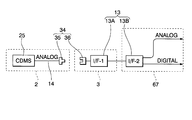
- the second substrate portion 13B is allowed to be disposed in the control box 67 outside the operation portion 3 while being disposed in the portion 3.
- the control box 67 that accommodates the second board portion 13B can be disposed in the vicinity of a monitor (video image display device) or a personal computer (not shown).
- FIG. 18A and FIG. 18B show a cross section of an insertion portion main body according to another embodiment.
- a hollow path 37E is added, and this hollow path 37E is used as a channel. It is a form to use as.
- the channel can be used for a supply path of nutrient solution or medicine. Although not shown, it is assumed that this channel has a mechanism that is attached and detached by attaching and detaching an insertion portion 2 and an operation portion 3 described later.
- the form shown in FIG. 18B is a form in which the wire for the bending operation is eliminated, and is preferably used not for the endoscope but for the catheter tube or the like.
- the means for irradiating light in front of the tip portion 16 is not limited to an optical fiber, and a semiconductor element (LED, light emitting element) that emits light is provided inside the tip portion 16 to replace the optical fiber.
- the power supplied to the LEDs is configured to be supplied from the interface board 13 by the collective coaxial cable 19 (second electric cable).
- the collective coaxial cable 19 is connected to the interface board 13 or in the middle of the interface board 13 by a connector.
- the electric power is configured to be supplied by connecting the male connection unit 14 and the female connection unit 15 and connecting the male connector unit 35 and the female connector unit 36.
- the present invention relates to an electronic endoscope using a solid-state imaging device, and can be applied particularly to an electronic endoscope in which an insertion portion inserted into a subject and an operation portion are detachable.
Landscapes
- Health & Medical Sciences (AREA)
- Life Sciences & Earth Sciences (AREA)
- Surgery (AREA)
- Biomedical Technology (AREA)
- Medical Informatics (AREA)
- Optics & Photonics (AREA)
- Pathology (AREA)
- Radiology & Medical Imaging (AREA)
- Biophysics (AREA)
- Engineering & Computer Science (AREA)
- Physics & Mathematics (AREA)
- Heart & Thoracic Surgery (AREA)
- Nuclear Medicine, Radiotherapy & Molecular Imaging (AREA)
- Molecular Biology (AREA)
- Animal Behavior & Ethology (AREA)
- General Health & Medical Sciences (AREA)
- Public Health (AREA)
- Veterinary Medicine (AREA)
- Endoscopes (AREA)
- Instruments For Viewing The Inside Of Hollow Bodies (AREA)
Abstract
L'invention fournit un endoscope électronique qui permet d'alléger la charge pour le patient, tout en présentant une partie insertion et une partie manipulation pouvant être attachées/détachées. Dans cet objectif, l'endoscope électronique de l'invention est équipé : de ladite partie insertion dont l'extrémité avant est à son tour équipée d'un élément d'imagerie à semi-conducteurs, et présentant une forme allongée qui s'insère dans un corps à examiner; et de ladite partie manipulation connectée de sorte à pouvoir être attachée/détachée par rapport à l'autre extrémité de la partie insertion. Au moins une portion d'un substrat d'interface qui émet en sortie des signaux d'image formés à partir de données brutes obtenues par l'élément d'imagerie à semi-conducteurs, est disposée au niveau de la partie interne de la partie manipulation. Un premier câble électrique qui transfert les données brutes obtenues par l'élément d'imagerie à semi-conducteurs, est connecté au substrat d'interface, ou sur le trajet allant à ce dernier, et est configuré de sorte à être attaché/détaché dans la section de connexion lorsque la partie insertion et attachée/détachée par rapport à la partie manipulation.
Priority Applications (2)
| Application Number | Priority Date | Filing Date | Title |
|---|---|---|---|
| CN201280023711.XA CN103533880A (zh) | 2011-06-06 | 2012-06-06 | 电子式内窥镜 |
| EP12797183.6A EP2689717A4 (fr) | 2011-06-06 | 2012-06-06 | Endoscope électronique |
Applications Claiming Priority (2)
| Application Number | Priority Date | Filing Date | Title |
|---|---|---|---|
| US201161493712P | 2011-06-06 | 2011-06-06 | |
| US61/493,712 | 2011-06-06 |
Publications (1)
| Publication Number | Publication Date |
|---|---|
| WO2012169511A1 true WO2012169511A1 (fr) | 2012-12-13 |
Family
ID=47262187
Family Applications (1)
| Application Number | Title | Priority Date | Filing Date |
|---|---|---|---|
| PCT/JP2012/064522 Ceased WO2012169511A1 (fr) | 2011-06-06 | 2012-06-06 | Endoscope électronique |
Country Status (5)
| Country | Link |
|---|---|
| US (1) | US20120310045A1 (fr) |
| EP (1) | EP2689717A4 (fr) |
| JP (1) | JPWO2012169511A1 (fr) |
| CN (1) | CN103533880A (fr) |
| WO (1) | WO2012169511A1 (fr) |
Cited By (10)
| Publication number | Priority date | Publication date | Assignee | Title |
|---|---|---|---|---|
| CN103417177A (zh) * | 2013-08-20 | 2013-12-04 | 姜泊 | 一种医用内窥镜插入组件 |
| CN103417178A (zh) * | 2013-08-20 | 2013-12-04 | 姜泊 | 一种一次性医用内窥镜 |
| JP2016504068A (ja) * | 2012-11-22 | 2016-02-12 | ジャイラス・エーシーエムアイ・インコーポレーテッド | 内視鏡カメラヘッドメモリ |
| JP2016077400A (ja) * | 2014-10-14 | 2016-05-16 | パナソニックIpマネジメント株式会社 | 内視鏡 |
| JP2017069600A (ja) * | 2015-09-28 | 2017-04-06 | 株式会社イチワ | 小型カメラ及び撮像装置 |
| CN107080513A (zh) * | 2017-05-17 | 2017-08-22 | 武汉佑康科技有限公司 | 一种模块化内窥镜 |
| JP2019037789A (ja) * | 2018-10-02 | 2019-03-14 | パナソニックIpマネジメント株式会社 | 内視鏡 |
| CN110446450A (zh) * | 2017-03-17 | 2019-11-12 | 国立大学法人大阪大学 | 软性内窥镜和具有该软性内窥镜的内窥镜系统 |
| JP2021087782A (ja) * | 2019-12-04 | 2021-06-10 | ショット アクチエンゲゼルシャフトSchott AG | 内視鏡、使い捨て内視鏡システムおよび内視鏡用の光源 |
| JP2021168841A (ja) * | 2020-04-17 | 2021-10-28 | エア・ウォーター株式会社 | 内視鏡装置及び内視鏡システム |
Families Citing this family (20)
| Publication number | Priority date | Publication date | Assignee | Title |
|---|---|---|---|---|
| JP6180405B2 (ja) | 2011-05-03 | 2017-08-16 | エンドーシー コーポレイションEndosee Corporation | ヒステロスコピー及び子宮内膜生検用の方法及び装置 |
| US9468367B2 (en) | 2012-05-14 | 2016-10-18 | Endosee Corporation | Method and apparatus for hysteroscopy and combined hysteroscopy and endometrial biopsy |
| US9622646B2 (en) | 2012-06-25 | 2017-04-18 | Coopersurgical, Inc. | Low-cost instrument for endoscopically guided operative procedures |
| US9492069B2 (en) * | 2012-07-03 | 2016-11-15 | Covidien Lp | Surgical camera assemblies and systems |
| JP5546597B2 (ja) * | 2012-08-30 | 2014-07-09 | 株式会社フジクラ | 医療機器用ハーネス及び医療機器の組立方法 |
| CN103908213A (zh) * | 2012-12-29 | 2014-07-09 | 上海澳华光电内窥镜有限公司 | 一种脱卸式内视镜装置 |
| JP5748790B2 (ja) * | 2013-02-27 | 2015-07-15 | 富士フイルム株式会社 | 電子内視鏡、及び電子内視鏡の製造方法 |
| US20140275763A1 (en) * | 2013-03-15 | 2014-09-18 | Lucent Medical Systems, Inc. | Partially disposable endoscopic device |
| JP5782064B2 (ja) * | 2013-04-15 | 2015-09-24 | 富士フイルム株式会社 | 内視鏡システム |
| EP3202305B1 (fr) * | 2014-09-29 | 2020-07-01 | Dong, Tao | Endoscope jetable et système associé |
| US10702305B2 (en) | 2016-03-23 | 2020-07-07 | Coopersurgical, Inc. | Operative cannulas and related methods |
| CN110325098A (zh) * | 2016-11-28 | 2019-10-11 | 适内有限责任公司 | 具有可分离一次性轴的内窥镜 |
| US20180228361A1 (en) * | 2017-02-15 | 2018-08-16 | Dynacolor, Inc. | Arthroscopic system with disposable arthroscope |
| US11109747B2 (en) * | 2017-02-15 | 2021-09-07 | Dynacolor, Inc. | Arthroscopic system with disposable arthroscope having image rotation function and method thereof |
| JP6800109B2 (ja) * | 2017-08-22 | 2020-12-16 | オリンパス株式会社 | 超音波内視鏡 |
| KR20250043601A (ko) * | 2018-06-08 | 2025-03-28 | 프리스틴 써지컬 엘엘씨 | 일회용 카메라 샤프트 및 재사용 가능한 손잡이를 갖는 내시경 |
| CN111839435B (zh) * | 2019-04-30 | 2024-09-27 | 新儿护科技医疗器材股份有限公司 | 可更换气管套的内视镜结构 |
| JP7536472B2 (ja) * | 2020-03-03 | 2024-08-20 | Hoya株式会社 | 内視鏡システム |
| JP2024515024A (ja) * | 2021-03-25 | 2024-04-04 | ヘルスケア・コンポーネンツ・グループ | 内視鏡 |
| US20220354357A1 (en) * | 2021-05-06 | 2022-11-10 | The Board Of Regents Of The University Of Texas System | Systems and apparatuses for performing an endoscopy with a detachable insertion cord |
Citations (6)
| Publication number | Priority date | Publication date | Assignee | Title |
|---|---|---|---|---|
| JPH0424018A (ja) * | 1990-05-21 | 1992-01-28 | Fuji Photo Optical Co Ltd | 電子内視鏡 |
| JPH05168591A (ja) * | 1991-12-20 | 1993-07-02 | Fuji Photo Optical Co Ltd | 電子内視鏡用処理ユニットの構造 |
| JPH06254047A (ja) | 1993-03-01 | 1994-09-13 | Olympus Optical Co Ltd | 内視鏡 |
| JP2001061777A (ja) * | 1999-08-26 | 2001-03-13 | Olympus Optical Co Ltd | 電子内視鏡 |
| JP2011036331A (ja) * | 2009-08-07 | 2011-02-24 | Olympus Medical Systems Corp | 電子内視鏡装置 |
| JP2011036414A (ja) * | 2009-08-11 | 2011-02-24 | Hoya Corp | 電子内視鏡および電子内視鏡システム |
Family Cites Families (4)
| Publication number | Priority date | Publication date | Assignee | Title |
|---|---|---|---|---|
| US5609561A (en) * | 1992-06-09 | 1997-03-11 | Olympus Optical Co., Ltd | Electronic type endoscope in which image pickup unit is dismounted to execute disinfection/sterilization processing |
| US6796939B1 (en) * | 1999-08-26 | 2004-09-28 | Olympus Corporation | Electronic endoscope |
| CN100512744C (zh) * | 2004-03-02 | 2009-07-15 | 奥林巴斯株式会社 | 内窥镜 |
| JP2006158859A (ja) * | 2004-12-10 | 2006-06-22 | Olympus Corp | 内視鏡及び内視鏡システム |
-
2012
- 2012-06-01 US US13/486,838 patent/US20120310045A1/en not_active Abandoned
- 2012-06-06 JP JP2013519496A patent/JPWO2012169511A1/ja active Pending
- 2012-06-06 EP EP12797183.6A patent/EP2689717A4/fr not_active Withdrawn
- 2012-06-06 CN CN201280023711.XA patent/CN103533880A/zh active Pending
- 2012-06-06 WO PCT/JP2012/064522 patent/WO2012169511A1/fr not_active Ceased
Patent Citations (6)
| Publication number | Priority date | Publication date | Assignee | Title |
|---|---|---|---|---|
| JPH0424018A (ja) * | 1990-05-21 | 1992-01-28 | Fuji Photo Optical Co Ltd | 電子内視鏡 |
| JPH05168591A (ja) * | 1991-12-20 | 1993-07-02 | Fuji Photo Optical Co Ltd | 電子内視鏡用処理ユニットの構造 |
| JPH06254047A (ja) | 1993-03-01 | 1994-09-13 | Olympus Optical Co Ltd | 内視鏡 |
| JP2001061777A (ja) * | 1999-08-26 | 2001-03-13 | Olympus Optical Co Ltd | 電子内視鏡 |
| JP2011036331A (ja) * | 2009-08-07 | 2011-02-24 | Olympus Medical Systems Corp | 電子内視鏡装置 |
| JP2011036414A (ja) * | 2009-08-11 | 2011-02-24 | Hoya Corp | 電子内視鏡および電子内視鏡システム |
Non-Patent Citations (1)
| Title |
|---|
| See also references of EP2689717A4 |
Cited By (14)
| Publication number | Priority date | Publication date | Assignee | Title |
|---|---|---|---|---|
| JP2016504068A (ja) * | 2012-11-22 | 2016-02-12 | ジャイラス・エーシーエムアイ・インコーポレーテッド | 内視鏡カメラヘッドメモリ |
| CN103417177A (zh) * | 2013-08-20 | 2013-12-04 | 姜泊 | 一种医用内窥镜插入组件 |
| CN103417178A (zh) * | 2013-08-20 | 2013-12-04 | 姜泊 | 一种一次性医用内窥镜 |
| CN103417177B (zh) * | 2013-08-20 | 2016-01-27 | 姜泊 | 一种医用内窥镜插入组件 |
| JP2016077400A (ja) * | 2014-10-14 | 2016-05-16 | パナソニックIpマネジメント株式会社 | 内視鏡 |
| US10555664B2 (en) | 2014-10-14 | 2020-02-11 | Panasonic I-Pro Sensing Solutions Co., Ltd. | Endoscope |
| JP2017069600A (ja) * | 2015-09-28 | 2017-04-06 | 株式会社イチワ | 小型カメラ及び撮像装置 |
| CN110446450A (zh) * | 2017-03-17 | 2019-11-12 | 国立大学法人大阪大学 | 软性内窥镜和具有该软性内窥镜的内窥镜系统 |
| CN110446450B (zh) * | 2017-03-17 | 2021-10-01 | 国立大学法人大阪大学 | 软性内窥镜和具有该软性内窥镜的内窥镜系统 |
| CN107080513B (zh) * | 2017-05-17 | 2018-10-16 | 武汉佑康科技有限公司 | 一种模块化内窥镜 |
| CN107080513A (zh) * | 2017-05-17 | 2017-08-22 | 武汉佑康科技有限公司 | 一种模块化内窥镜 |
| JP2019037789A (ja) * | 2018-10-02 | 2019-03-14 | パナソニックIpマネジメント株式会社 | 内視鏡 |
| JP2021087782A (ja) * | 2019-12-04 | 2021-06-10 | ショット アクチエンゲゼルシャフトSchott AG | 内視鏡、使い捨て内視鏡システムおよび内視鏡用の光源 |
| JP2021168841A (ja) * | 2020-04-17 | 2021-10-28 | エア・ウォーター株式会社 | 内視鏡装置及び内視鏡システム |
Also Published As
| Publication number | Publication date |
|---|---|
| CN103533880A (zh) | 2014-01-22 |
| JPWO2012169511A1 (ja) | 2015-02-23 |
| EP2689717A4 (fr) | 2014-09-17 |
| EP2689717A1 (fr) | 2014-01-29 |
| US20120310045A1 (en) | 2012-12-06 |
Similar Documents
| Publication | Publication Date | Title |
|---|---|---|
| WO2012169511A1 (fr) | Endoscope électronique | |
| JP5308716B2 (ja) | 電子内視鏡装置 | |
| US9247867B2 (en) | Endoscopic arrangement | |
| JP5857047B2 (ja) | 電子式内視鏡の撮像部構造 | |
| US8235887B2 (en) | Endoscope assembly with retroscope | |
| CN110151098A (zh) | 视野偏离中心方向的内窥镜系统 | |
| EP1986541A2 (fr) | Endoscope | |
| WO2015163942A1 (fr) | Système d'imagerie médicale intégré | |
| US10687696B2 (en) | Endoscope system with communication mode stabilizing unit | |
| CN114652355A (zh) | 超声波内窥镜 | |
| WO2018155066A1 (fr) | Endoscope | |
| CN102946786B (zh) | 激光视频内窥镜 | |
| WO2023019830A1 (fr) | Ensemble d'imagerie intégré, endoscope et procédé de récupération | |
| JP2010005148A (ja) | 内視鏡及び内視鏡の信号伝送方法 | |
| WO2014188787A1 (fr) | Structure d'extrémité d'endoscope et endoscope | |
| JP5513169B2 (ja) | 内視鏡 | |
| JPWO2015194460A1 (ja) | ケーブル接続構造および内視鏡装置 | |
| CN105007803B (zh) | 摄像单元 | |
| JP2011177263A (ja) | 内視鏡 | |
| JP7759868B2 (ja) | 医療用観察システムおよび伝送ケーブル | |
| JP6744118B2 (ja) | 内視鏡 | |
| JP2009183380A (ja) | 検診用内視鏡 | |
| JP2005288085A (ja) | カプセル内視鏡 | |
| JP2008093454A (ja) | 内視鏡装置 | |
| JP2009165623A (ja) | 検診用内視鏡 |
Legal Events
| Date | Code | Title | Description |
|---|---|---|---|
| 121 | Ep: the epo has been informed by wipo that ep was designated in this application |
Ref document number: 12797183 Country of ref document: EP Kind code of ref document: A1 |
|
| ENP | Entry into the national phase |
Ref document number: 2013519496 Country of ref document: JP Kind code of ref document: A |
|
| WWE | Wipo information: entry into national phase |
Ref document number: 2012797183 Country of ref document: EP |
|
| NENP | Non-entry into the national phase |
Ref country code: DE |