WO2012169788A2 - Plaquette de silicium monocristallin et son procédé de fabrication - Google Patents
Plaquette de silicium monocristallin et son procédé de fabrication Download PDFInfo
- Publication number
- WO2012169788A2 WO2012169788A2 PCT/KR2012/004479 KR2012004479W WO2012169788A2 WO 2012169788 A2 WO2012169788 A2 WO 2012169788A2 KR 2012004479 W KR2012004479 W KR 2012004479W WO 2012169788 A2 WO2012169788 A2 WO 2012169788A2
- Authority
- WO
- WIPO (PCT)
- Prior art keywords
- silicon wafer
- single crystal
- crystal silicon
- pyramid
- compounds
- Prior art date
- Legal status (The legal status is an assumption and is not a legal conclusion. Google has not performed a legal analysis and makes no representation as to the accuracy of the status listed.)
- Ceased
Links
Images


Classifications
-
- C—CHEMISTRY; METALLURGY
- C30—CRYSTAL GROWTH
- C30B—SINGLE-CRYSTAL GROWTH; UNIDIRECTIONAL SOLIDIFICATION OF EUTECTIC MATERIAL OR UNIDIRECTIONAL DEMIXING OF EUTECTOID MATERIAL; REFINING BY ZONE-MELTING OF MATERIAL; PRODUCTION OF A HOMOGENEOUS POLYCRYSTALLINE MATERIAL WITH DEFINED STRUCTURE; SINGLE CRYSTALS OR HOMOGENEOUS POLYCRYSTALLINE MATERIAL WITH DEFINED STRUCTURE; AFTER-TREATMENT OF SINGLE CRYSTALS OR A HOMOGENEOUS POLYCRYSTALLINE MATERIAL WITH DEFINED STRUCTURE; APPARATUS THEREFOR
- C30B29/00—Single crystals or homogeneous polycrystalline material with defined structure characterised by the material or by their shape
- C30B29/02—Elements
- C30B29/06—Silicon
Definitions
- the present invention relates to a single crystal silicon wafer capable of maximizing the absorption of sunlight and significantly lowering the light reflectivity and further increasing the light efficiency, and a method of manufacturing the same.
- Solar cells which are rapidly spreading in recent years, are electronic devices that directly convert solar energy, which is clean energy, into electricity as a next-generation energy source, and diffuse phosphorus on its surface based on P-type silicon semiconductors containing boron in silicon. It consists of the PN junction semiconductor substrate in which the N type silicon semiconductor layer was formed.
- the surface of the solar cell silicon wafer constituting the PN junction semiconductor substrate is formed into a fine pyramid structure and the anti-reflection film is treated.
- the fine pyramid formed on the silicon wafer surface is a square pyramid in which a rectangular bottom surface B and four triangular side surfaces S meet at one vertex.
- the side of the micro-pyramids (S 1), as shown in Figure 2 the vertices (a 1) 2 of sides meets the base line (b 1) constituting the bottom surface from (c 11, c 12) of the triangle is a straight line Form.
- the silicon wafer formed with the fine pyramid structure can increase the efficiency of the solar cell by decreasing the reflectance of the incident light having a wide wavelength band and increasing the intensity of the absorbed light. The efficiency can be further increased.
- An object of the present invention is to provide a single crystal silicon wafer having a structure capable of maximizing the absorption of sunlight and significantly lowering the light reflectance.
- Another object of the present invention is to provide a method for manufacturing a single crystal silicon wafer having a fine pyramid structure easily without using an etching mask.
- a single crystal silicon wafer having a surface on which a pyramid with a curved side from one vertex to a bottom surface is repeatedly formed.
- the etching liquid composition is a single crystal silicon wafer containing 0.1 to 20% by weight and 80 to 99.9% by weight of the alkali compound.
- alkali compound is at least one selected from the group consisting of potassium hydroxide, sodium hydroxide, ammonium hydroxide, tetrahydroxymethylammonium and tetrahydroxyethylammonium.
- the etching liquid composition is a single crystal silicon wafer further comprises 10 to 6 to 10% by weight of the cyclic compound containing a nitrogen atom, bonded to a functional group containing an alken group having 2 to 6 carbon atoms.
- the cyclic compound is N-vinylpiperazine, N-vinylmethylpiperazine, N-vinylethylpiperazine, N-vinyl-N'-methylpiperazine, N-acryloylpiperazine, N-acryloyl-N'-methylpiperazine, N-vinylmorpholine, N-vinylmethylmorpholine, N-vinylethylmorpholine, N-acryloylmorpholine, N-vinylpiperidone, N-vinyl Methylpiperidone, N-vinylethylpiperidone, N-acryloylpiperidone, N-vinylpyrrolidone, N-vinylmethylpyrrolidone, N-vinylethyl-2-pyrrolidone, N-acryloylpyrroli A monocrystalline silicon wafer, which is at least one member selected from the group consisting of don, N-vinylcarbazole and N-acryloylcarbazol
- the etchant composition further comprises at least one polysaccharide selected from the group consisting of glucan-based compounds, fructan-based compounds, mannan-based compounds, galactan-based compounds, and metal salts thereof.
- a method of manufacturing a single crystal silicon wafer comprising.
- etching solution composition is an etching solution composition of 0.1 to 20% by weight of the alkali compound and 80 to 99.9% by weight of a method for producing a single crystal silicon wafer.
- alkali compound is at least one selected from the group consisting of potassium hydroxide, sodium hydroxide, ammonium hydroxide, tetrahydroxymethylammonium and tetrahydroxyethylammonium.
- the etchant composition further comprises 10 -6 to 10% by weight of a cyclic compound containing a nitrogen atom to which a functional group including an alkene group having 2 to 6 carbon atoms is bonded. Way.
- the cyclic compound is N-vinylpiperazine, N-vinylmethylpiperazine, N-vinylethylpiperazine, N-vinyl-N'-methylpiperazine, N-acryloylpiperazine, N-acryloyl-N'-methylpiperazine, N-vinylmorpholine, N-vinylmethylmorpholine, N-vinylethylmorpholine, N-acryloylmorpholine, N-vinylpiperidone, N-vinyl Methylpiperidone, N-vinylethylpiperidone, N-acryloylpiperidone, N-vinylpyrrolidone, N-vinylmethylpyrrolidone, N-vinylethyl-2-pyrrolidone, N-acryloylpyrroli A method for producing a single crystal silicon wafer, which is at least one selected from the group consisting of don, N-vinylcarbazole and
- the etching solution composition further comprises one or more polysaccharides selected from the group consisting of glucan-based compounds, fructan-based compounds, mannan-based compounds, galactan-based compounds and metal salts thereof. .
- the single crystal silicon wafer of the present invention has a surface composed of a plurality of fine pyramids having curved side surfaces, the absorption efficiency of the solar light can be maximized and the light reflectance can be greatly reduced to further increase the light efficiency.
- the method for manufacturing a single crystal silicon wafer of the present invention can form a large number of fine pyramid structures having curved side surfaces without using an etching mask, and thus has excellent productivity.
- FIG. 1 is a perspective view of a fine pyramid formed on a surface of a conventional single crystal silicon wafer
- Figure 2 is a cross-sectional view showing one side of a fine pyramid formed on the surface of a conventional single crystal silicon wafer
- FIG. 3 is a cross-sectional view showing one side of a fine pyramid formed on the surface of a single crystal silicon wafer of the present invention
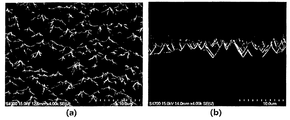
- FIG. 4 is a SEM photograph showing the surface (a) and the cross section (b) of the fine pyramid formed on the surface of the silicon wafer according to an embodiment of the present invention
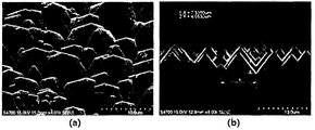
- FIG. 5 is a SEM photograph showing the surface (a) and the cross section (b) of the fine pyramid formed on the surface of a conventional silicon wafer,
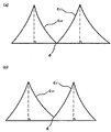
- FIG. 6 is a vertical cross-sectional view of two different pyramids formed on a silicon surface adjacent to each other according to an embodiment of the present invention.
- the present invention relates to a single crystal silicon wafer capable of maximizing the absorption of sunlight and significantly lowering the light reflectivity and further increasing the light efficiency, and a method of manufacturing the same.
- a pyramid means a quadrangular pyramid formed by meeting a bottom surface B having a quadrangle and four side faces S having a triangle at one vertex.
- the single crystal silicon wafer of the present invention is characterized by having a surface on which a pyramid having a curved side from one vertex to a bottom surface is repeatedly formed.
- the side surface S 2 of the pyramid has a straight line between two side edges c 21 and c 22 that meet the base side b 2 constituting the bottom surface from the vertex a 2 . Is not a curve. That is, the side surface S 2 becomes a curved surface.
- the two sides c 21 , c 22 constituting one side of the pyramid may be curved in the same or different shape. That is, when the side surface is divided from the vertex a 2 into the center line L perpendicular to the base side b 2 , the two divided surfaces may be the same (FIG. 3A) or different from each other (FIG. 3B).
- the vertical cross-section of the shape formed by the side of the pyramid and the side of the other pyramid adjacent to the pyramid may have a point (d).
- the point of the present invention is a tangent point formed by the side (c 21 ) of one pyramid and the side (c 22 ) of the other pyramid adjacent thereto.
- the fine point may be formed on the surface of the single crystal silicon wafer as shown in FIG. 6 (a), or when the tangent of two asymmetric pyramids as shown in FIG. 6 (b) is located above the surface of the single crystal silicon wafer. It may be formed on the upper side of the surface.
- the wafer according to the present invention has the structure as shown in FIG. 6, the effect of improving the light efficiency can be further increased.
- a pyramid structure of the present invention can be obtained by etching directly with an etchant composition without using an etching mask, and if an etching mask is used, a portion where the pyramid and the pyramid meet inevitably forms a curved surface. It is not possible to obtain a repeated pyramid structure with a corresponding peak.
- the sides of the pyramid may be curved to convex toward the center.
- one or more of the four sides constituting the pyramid may be a curved surface as described above.
- Repeated formation of the pyramid indicates, for example, that a plurality of pyramids having the above shape exist on the surface of the wafer as shown in FIG. 4, provided that a plurality of pyramids having curved surfaces from one vertex to the bottom surface are formed. , Not only when a plurality of pyramids of the same shape are formed, but also pyramids of different shapes (for example, pyramids of the shapes of FIGS. 3A and 3B, pyramids of different sizes L, etc.) are mixed. Also included in the case where a plurality of pyramids of the present application are formed repeatedly.
- Repeatedly formed pyramids do not necessarily have to occupy an area over a percentage of the surface area of the wafer. However, in order to contribute to maximizing the absorption amount of sunlight and lowering the light reflectance, it is preferable to form at least 50% of the surface area of the wafer, preferably at least 70%.
- the size of the micro pyramid is preferably several nanometers.
- 70% or more of the pyramids constituting the single crystal silicon wafer surface have an average size of 1 to 6 mu m.
- the average size of the pyramid means the length of the line extending from one vertex perpendicular to the bottom surface.
- the method of the present invention for repeatedly forming the pyramid whose curved side surface from one vertex to the bottom surface according to the present invention on the surface of the single crystal silicon wafer is characterized by not using an etching mask.
- the surface of the single crystal silicon wafer may be formed as a fine pyramid structure according to the present invention by a texture etching method using an alkaline etching solution composition without using an etching mask.
- the etching solution composition according to the present invention may be one containing 0.1 to 20% by weight of the alkali compound and 80 to 99.9% by weight of water.
- an etching liquid composition further contains the cyclic compound containing a nitrogen atom to which the functional group containing a C2-C6 alkene group couple
- An alkali compound is a component which etches the surface of a crystalline silicon wafer,
- the kind is not specifically limited.
- potassium hydroxide, sodium hydroxide, ammonium hydroxide, tetrahydroxymethylammonium, tetrahydroxyethylammonium, etc. are mentioned, Among these, potassium hydroxide and sodium hydroxide are preferable. These can be used individually or in mixture of 2 or more types.
- an alkali compound is contained in 0.1 to 20 weight% with respect to 100 weight% of etching liquid compositions, More preferably, it is 1 to 5 weight%. When the content falls within the above range, the silicon wafer surface can be etched.
- the cyclic compound containing a nitrogen atom to which a functional group containing an alkene group having 2 to 6 carbon atoms is bonded controls the etching rate difference between the Si 100 direction and the Si 111 direction, which are the crystal directions of silicon, so that the pyramid is It is a component that adjusts the shape to have a curved side.
- Examples of the cyclic compound include N-vinylpiperazine, N-vinylmethylpiperazine, N-vinylethylpiperazine, N-vinyl-N'-methylpiperazine, N-acryloylpiperazine, N-acryloyl- N'-methylpiperazine, N-vinylmorpholine, N-vinylmethylmorpholine, N-vinylethylmorpholine, N-acryloylmorpholine, N-vinylpiperidone, N-vinylmethylpiperidone, N- Vinylethylpiperidone, N-acryloylpiperidone, N-vinylpyrrolidone, N-vinylmethylpyrrolidone, N-vinylethyl-2-pyrrolidone, N-acryloylpyrrolidone, N-vinylcarba A sol, N-acryloyl carbazole, etc. are mentioned, These can be used individually or in mixture of 2 or more types.
- the cyclic compound is preferably contained in an amount of 10 -6 to 10% by weight, more preferably 10 -3 to 1% by weight based on 100% by weight of the etching liquid composition.
- the content falls within the above range, the wettability of the surface of the silicon wafer may be effectively improved to minimize texture quality variation and to easily form a fine pyramid having a different shape from the conventional one. If the content is more than 10% by weight, it may be difficult to control the etching rate difference with respect to the crystal direction of the silicon, and thus it may be difficult to obtain the desired fine pyramid formation.
- the etching solution composition may further include a polysaccharide.
- Polysaccharides are saccharides in which two or more monosaccharides are glycosidic bonds to form large molecules.
- the polysaccharides form a uniform fine pyramid by preventing over-etching and accelerated etching by alkali compounds, and at the same time, they form hydrogen bubbles generated by etching. It is a component that improves the appearance by quickly dropping from the surface of the silicon wafer.
- polysaccharides examples include glucan compounds, fructan compounds, mannan compounds, galactan compounds, or metal salts thereof, among which glucan compounds and metal salts thereof are preferable. Do. These can be used individually or in mixture of 2 or more types.
- glucan compound examples include cellulose, dimethylaminoethyl cellulose, diethylaminoethyl cellulose, ethyl hydroxyethyl cellulose, methyl hydroxyethyl cellulose, 4-aminobenzyl cellulose, triethylaminoethyl cellulose, cyanoethyl cellulose, ethyl cellulose, Methyl cellulose, carboxymethyl cellulose, hydroxyethyl cellulose, hydroxypropyl cellulose, alginic acid, amylose, amylopectin, pectin, starch, dextrin, ⁇ -cyclodextrin, ⁇ -cyclodextrin, ⁇ -cyclodextrin, hydroxypropyl- ⁇ -Cyclodextrin, methyl- beta -cyclodextrin, dextran, dextransulfate sodium, saponin, glycogen, zymoic acid, lentinan, s
- the polysaccharide may have an average molecular weight of 5,000 to 1,000,000, preferably 50,000 to 200,000.
- the polysaccharide may be included in an amount of 10 -9 to 10% by weight, preferably 10 -6 to 1% by weight, based on 100% by weight of the etching solution composition. If the content falls within the above range, it is possible to effectively prevent over-etching and etching acceleration. If the content is more than 10% by weight, it is difficult to form the desired fine pyramid by drastically lowering the etching rate by the alkali compound.
- the texture etching liquid composition of the crystalline silicon wafer of the present invention may further include at least one of a surfactant, a fatty acid and an alkali metal salt thereof, a silica-containing compound and the like.
- the kind of water is not specifically limited, It is preferable that it is deionized distilled water, More preferably, it is preferable that the specific resistance value is 18 kW / cm or more as deionized distilled water for a semiconductor process.
- Water may be included in the balance in a total of 100% by weight of the crystalline etching solution composition.
- the kind of water is not specifically limited, It is preferable that it is deionized distilled water, More preferably, it is preferable that the specific resistance value is 18 kW / cm or more as deionized distilled water for a semiconductor process.
- the surface of the structure made of a fine pyramid may be formed by a method including depositing, spraying, or depositing and spraying a single crystal silicon wafer using the etching solution composition configured as described above.
- the number of depositions and sprays is not particularly limited, and the order of both deposition and spraying is not limited.
- the step of depositing, spraying or depositing and spraying may be carried out for 30 seconds to 60 minutes at a temperature of 50 to 100 °C. At this time, an etching process such as a dip method, a spray method or a single sheet method may be used.
- An etching solution composition was prepared by mixing 2% by weight of potassium hydroxide (KOH), 0.1% by weight of N-vinylpyrrolidone, 0.02% by weight of sodium alginate (AANa), and residual deionized distilled water.
- KOH potassium hydroxide
- AANa sodium alginate
- the single crystal silicon wafer substrate was texture etched by dipping the prepared etching liquid composition at a temperature of 80 ° C. for 20 minutes.
- An etching solution composition was prepared by mixing 2% by weight of potassium hydroxide (KOH), 0.1% by weight of N-methylpyrrolidone, 0.02% by weight of sodium alginate (AANa), and residual deionized distilled water.
- KOH potassium hydroxide
- AANa sodium alginate
- the single crystal silicon wafer substrate was texture etched by dipping the prepared etching liquid composition at a temperature of 80 ° C. for 20 minutes.
- the shape of the fine pyramid structure formed on the surface of the single crystal silicon wafer substrate was confirmed using a scanning electron microscope (SEM).
- the variation, i.e., uniformity, of the fine pyramid structure formed on the surface of the single crystal silicon wafer substrate was visually observed using a digital camera, a 3D optical microscope, and a scanning electron microscope (SEM), and evaluated based on the following criteria.
- the reflectance at the time of irradiating the light of 600 nm wavelength band using the UV spectrophotometer to the surface of a single crystal silicon wafer substrate was measured.
- Example 4 and 5 are SEM photographs showing the surfaces of the single crystal silicon wafer substrates texture-etched in Example 1 and Comparative Example 1, respectively. Looking in detail, it can be seen that the fine pyramid formed in Example 1 is formed in a shape in which two side edges that meet the bottom surface from one vertex are curved, that is, the sides are curved, and the size is small and uniform.
- the fine pyramid formed in Comparative Example 1 is formed in a form in which the two side edges that meet the bottom surface from one vertex is a straight shape, that is, the side is a flat surface, the size is also larger than Example 1.
- the single crystal silicon wafer according to the present invention can maximize the amount of absorption of sunlight and lower the light reflectance due to the difference in shape of the fine pyramid.
- the single crystal silicon wafer substrate of Example 1 having a plurality of fine pyramids having curved sides according to the present invention is excellent in uniformity of the fine pyramid texture as compared to the substrate of Comparative Example 1.
- the light reflectance is lower than that of Comparative Example 1 due to the shape of the fine pyramid. This can further increase the light efficiency.
Landscapes
- Chemical & Material Sciences (AREA)
- Engineering & Computer Science (AREA)
- Crystallography & Structural Chemistry (AREA)
- Materials Engineering (AREA)
- Metallurgy (AREA)
- Organic Chemistry (AREA)
- Crystals, And After-Treatments Of Crystals (AREA)
- Liquid Deposition Of Substances Of Which Semiconductor Devices Are Composed (AREA)
- Photovoltaic Devices (AREA)
- Weting (AREA)
Abstract
Cette invention concerne une plaquette de silicium monocristallin et son procédé de fabrication, et plus spécifiquement : une plaquette de silicium cristallin qui peut en outre accroître le rendement lumineux par optimisation de la quantité de lumière absorbée et abaissement visible de la réflectance de la lumière, ladite plaquette de silicium cristallin étant conçue pour présenter une surface constituée d'une pluralité de pyramides dont une face latérale allant du sommet jusqu'à la base est incurvée ; et son procédé de fabrication.
Priority Applications (1)
| Application Number | Priority Date | Filing Date | Title |
|---|---|---|---|
| CN201280024299.3A CN103563093B (zh) | 2011-06-07 | 2012-06-07 | 单晶硅片及其制备方法 |
Applications Claiming Priority (6)
| Application Number | Priority Date | Filing Date | Title |
|---|---|---|---|
| KR10-2011-0054569 | 2011-06-07 | ||
| KR20110054569 | 2011-06-07 | ||
| KR10-2012-0059142 | 2012-06-01 | ||
| KR1020120059142A KR20120135870A (ko) | 2011-06-07 | 2012-06-01 | 단결정 실리콘 웨이퍼 및 그 제조방법 |
| KR1020120059966A KR101896619B1 (ko) | 2011-06-07 | 2012-06-04 | 단결정 실리콘 웨이퍼 및 그 제조방법 |
| KR10-2012-0059966 | 2012-06-04 |
Publications (2)
| Publication Number | Publication Date |
|---|---|
| WO2012169788A2 true WO2012169788A2 (fr) | 2012-12-13 |
| WO2012169788A3 WO2012169788A3 (fr) | 2013-03-07 |
Family
ID=47296592
Family Applications (1)
| Application Number | Title | Priority Date | Filing Date |
|---|---|---|---|
| PCT/KR2012/004479 Ceased WO2012169788A2 (fr) | 2011-06-07 | 2012-06-07 | Plaquette de silicium monocristallin et son procédé de fabrication |
Country Status (1)
| Country | Link |
|---|---|
| WO (1) | WO2012169788A2 (fr) |
Cited By (3)
| Publication number | Priority date | Publication date | Assignee | Title |
|---|---|---|---|---|
| CN103346209A (zh) * | 2013-06-24 | 2013-10-09 | 陕西师范大学 | 用于增强太阳光利用率的表面修饰基材及修饰方法和应用 |
| CN104393104A (zh) * | 2014-10-17 | 2015-03-04 | 深圳华中科技大学研究院 | 一种用于hit太阳电池织构的处理技术 |
| WO2019220440A1 (fr) * | 2018-05-15 | 2019-11-21 | B.G. Negev Technologies And Applications Ltd., At Ben-Gurion University | Structure de surface d'absorption optique de dispositifs d'absorption de lumière |
Family Cites Families (3)
| Publication number | Priority date | Publication date | Assignee | Title |
|---|---|---|---|---|
| WO2009120631A2 (fr) * | 2008-03-25 | 2009-10-01 | Applied Materials, Inc. | Procédé de nettoyage et de texturation de surface pour cellules solaires cristallines |
| JP4937233B2 (ja) * | 2008-11-19 | 2012-05-23 | 三菱電機株式会社 | 太陽電池用基板の粗面化方法および太陽電池セルの製造方法 |
| US7955989B2 (en) * | 2009-09-24 | 2011-06-07 | Rohm And Haas Electronic Materials Llc | Texturing semiconductor substrates |
-
2012
- 2012-06-07 WO PCT/KR2012/004479 patent/WO2012169788A2/fr not_active Ceased
Cited By (3)
| Publication number | Priority date | Publication date | Assignee | Title |
|---|---|---|---|---|
| CN103346209A (zh) * | 2013-06-24 | 2013-10-09 | 陕西师范大学 | 用于增强太阳光利用率的表面修饰基材及修饰方法和应用 |
| CN104393104A (zh) * | 2014-10-17 | 2015-03-04 | 深圳华中科技大学研究院 | 一种用于hit太阳电池织构的处理技术 |
| WO2019220440A1 (fr) * | 2018-05-15 | 2019-11-21 | B.G. Negev Technologies And Applications Ltd., At Ben-Gurion University | Structure de surface d'absorption optique de dispositifs d'absorption de lumière |
Also Published As
| Publication number | Publication date |
|---|---|
| WO2012169788A3 (fr) | 2013-03-07 |
Similar Documents
| Publication | Publication Date | Title |
|---|---|---|
| WO2012169721A1 (fr) | Composition de type solution de gravage texturante et procédé de gravage texturant pour plaquette de silicium cristallin | |
| CN103339739B (zh) | 太阳能电池的丝网印刷板及印刷太阳能电池的电极的方法 | |
| WO2011046365A2 (fr) | Composition de pâte à l'argent et pile solaire l'utilisant | |
| CN104488089A (zh) | 钝化层形成用组合物、带钝化层的半导体基板、带钝化层的半导体基板的制造方法、太阳能电池元件、太阳能电池元件的制造方法及太阳能电池 | |
| WO2012169722A1 (fr) | Composition de type solution de gravage texturante et procédé de gravage texturant pour plaquette de silicium cristallin | |
| WO2012144733A2 (fr) | Composition d'agent de gravure pour texturation pour tranche de silicium cristallin et procédé de gravure pour texturation | |
| CN104471717A (zh) | 钝化层形成用组合物、带钝化层的半导体基板、带钝化层的半导体基板的制造方法、太阳能电池元件、太阳能电池元件的制造方法及太阳能电池 | |
| JP2011139023A (ja) | 半導体基体のテクスチャ化 | |
| CN102169738A (zh) | 形成p型扩散层的组合物和方法及制备光伏电池的方法 | |
| CN103563093B (zh) | 单晶硅片及其制备方法 | |
| WO2015012457A1 (fr) | Plaquette de silicium possédant une structure complexe, son procédé de fabrication et cellule solaire l'utilisant | |
| KR20140117400A (ko) | 패시베이션막이 있는 반도체 기판과 그 제조 방법, 및 태양전지 소자와 그 제조 방법 | |
| CN104928680A (zh) | 结晶性硅片的纹理蚀刻液组合物和纹理蚀刻方法 | |
| Chen et al. | Improvement of conversion efficiency of multi-crystalline silicon solar cells using reactive ion etching with surface pre-etching | |
| WO2015133730A1 (fr) | Composition de gravure-texturation pour une tranche de silicium cristallin, et procédé de gravure-texturation | |
| TWI680979B (zh) | 鈍化層形成用組成物、帶鈍化層的半導體基板及其製造方法、太陽電池元件及其製造方法以及太陽電池 | |
| KR20140117399A (ko) | 패시베이션막 형성용 조성물, 패시베이션막이 있는 반도체 기판과 그 제조 방법, 및 태양전지 소자와 그 제조 방법 | |
| WO2013089338A1 (fr) | Composition pour solution de gravure de texture d'une plaquette de silicium cristallin, et procédé de gravure de texture | |
| KR20140082222A (ko) | 결정성 실리콘 웨이퍼의 텍스쳐 에칭액 조성물 및 텍스쳐 에칭방법 | |
| WO2013058477A2 (fr) | Composition fluide d'attaque chimique de texture et procédé d'attaque chimique de texture pour des tranches de silicium cristallin | |
| KR101892624B1 (ko) | 결정성 실리콘 웨이퍼의 텍스쳐 에칭액 조성물 및 텍스쳐 에칭방법 | |
| KR101994084B1 (ko) | 결정성 실리콘 웨이퍼의 텍스쳐 에칭액 조성물 및 텍스쳐 에칭방법 | |
| WO2015020243A1 (fr) | Composition de solution de gravure de texture pour plaquettes de silicium cristallin et procédé de gravure de texture | |
| WO2013002502A2 (fr) | Composition de gravure de texture pour une tranche de silicium cristallin et procédé de gravure de texture de celle-ci | |
| CN106784164B (zh) | 一种背面镀膜处理的太阳能电池制备工艺 |
Legal Events
| Date | Code | Title | Description |
|---|---|---|---|
| 121 | Ep: the epo has been informed by wipo that ep was designated in this application |
Ref document number: 12796453 Country of ref document: EP Kind code of ref document: A2 |
|
| NENP | Non-entry into the national phase |
Ref country code: DE |
|
| 122 | Ep: pct application non-entry in european phase |
Ref document number: 12796453 Country of ref document: EP Kind code of ref document: A2 |