WO2012172930A1 - Dispositif d'émission d'énergie électrique et système de réception d'énergie électrique - Google Patents
Dispositif d'émission d'énergie électrique et système de réception d'énergie électrique Download PDFInfo
- Publication number
- WO2012172930A1 WO2012172930A1 PCT/JP2012/062903 JP2012062903W WO2012172930A1 WO 2012172930 A1 WO2012172930 A1 WO 2012172930A1 JP 2012062903 W JP2012062903 W JP 2012062903W WO 2012172930 A1 WO2012172930 A1 WO 2012172930A1
- Authority
- WO
- WIPO (PCT)
- Prior art keywords
- device side
- power
- power transmission
- electrode
- transmission device
- Prior art date
- Legal status (The legal status is an assumption and is not a legal conclusion. Google has not performed a legal analysis and makes no representation as to the accuracy of the status listed.)
- Ceased
Links
Images




Classifications
-
- H—ELECTRICITY
- H02—GENERATION; CONVERSION OR DISTRIBUTION OF ELECTRIC POWER
- H02J—ELECTRIC POWER NETWORKS; CIRCUIT ARRANGEMENTS OR SYSTEMS FOR SUPPLYING OR DISTRIBUTING ELECTRIC POWER; SYSTEMS FOR STORING ELECTRIC ENERGY
- H02J7/00—Circuit arrangements for charging or discharging batteries or for supplying loads from batteries
- H02J7/02—Circuit arrangements for charging or discharging batteries or for supplying loads from batteries for charging batteries from AC mains by converters
-
- H—ELECTRICITY
- H02—GENERATION; CONVERSION OR DISTRIBUTION OF ELECTRIC POWER
- H02J—ELECTRIC POWER NETWORKS; CIRCUIT ARRANGEMENTS OR SYSTEMS FOR SUPPLYING OR DISTRIBUTING ELECTRIC POWER; SYSTEMS FOR STORING ELECTRIC ENERGY
- H02J50/00—Circuit arrangements or systems for wireless supply or distribution of electric power
- H02J50/05—Circuit arrangements or systems for wireless supply or distribution of electric power using capacitive coupling
-
- H—ELECTRICITY
- H02—GENERATION; CONVERSION OR DISTRIBUTION OF ELECTRIC POWER
- H02J—ELECTRIC POWER NETWORKS; CIRCUIT ARRANGEMENTS OR SYSTEMS FOR SUPPLYING OR DISTRIBUTING ELECTRIC POWER; SYSTEMS FOR STORING ELECTRIC ENERGY
- H02J50/00—Circuit arrangements or systems for wireless supply or distribution of electric power
- H02J50/90—Circuit arrangements or systems for wireless supply or distribution of electric power involving detection or optimisation of position, e.g. alignment
-
- H—ELECTRICITY
- H02—GENERATION; CONVERSION OR DISTRIBUTION OF ELECTRIC POWER
- H02J—ELECTRIC POWER NETWORKS; CIRCUIT ARRANGEMENTS OR SYSTEMS FOR SUPPLYING OR DISTRIBUTING ELECTRIC POWER; SYSTEMS FOR STORING ELECTRIC ENERGY
- H02J7/00—Circuit arrangements for charging or discharging batteries or for supplying loads from batteries
- H02J7/70—Circuit arrangements for charging or discharging batteries or for supplying loads from batteries characterised by the mechanical construction
- H02J7/731—Circuit arrangements for charging or discharging batteries or for supplying loads from batteries characterised by the mechanical construction specially adapted for holding portable devices containing batteries
-
- H—ELECTRICITY
- H02—GENERATION; CONVERSION OR DISTRIBUTION OF ELECTRIC POWER
- H02J—ELECTRIC POWER NETWORKS; CIRCUIT ARRANGEMENTS OR SYSTEMS FOR SUPPLYING OR DISTRIBUTING ELECTRIC POWER; SYSTEMS FOR STORING ELECTRIC ENERGY
- H02J2207/00—Details of circuit arrangements for charging or discharging batteries or supplying loads from batteries
- H02J2207/20—Charging or discharging characterised by the power electronics converter
-
- H—ELECTRICITY
- H02—GENERATION; CONVERSION OR DISTRIBUTION OF ELECTRIC POWER
- H02J—ELECTRIC POWER NETWORKS; CIRCUIT ARRANGEMENTS OR SYSTEMS FOR SUPPLYING OR DISTRIBUTING ELECTRIC POWER; SYSTEMS FOR STORING ELECTRIC ENERGY
- H02J50/00—Circuit arrangements or systems for wireless supply or distribution of electric power
- H02J50/70—Circuit arrangements or systems for wireless supply or distribution of electric power involving the reduction of electric, magnetic or electromagnetic leakage fields
Definitions
- the present invention relates to a power transmission device used in a power transmission system that transmits power by electric field coupling and the power transmission system.
- FIG. 1 is a diagram showing a basic configuration of the power transmission system disclosed in Patent Document 1.
- This power transmission system includes a power transmission device and a power reception device.
- the power transmission device includes a high frequency high voltage generation circuit 1, a passive electrode 2, and an active electrode 3.
- the power receiving device includes a high frequency high voltage load circuit 5, a passive electrode 7, and an active electrode 6. Then, when the active electrode 3 of the power transmission device and the active electrode 6 of the power reception device come close to each other through the high voltage electric field region 4, the two electrodes are subjected to electric field coupling.
- An electrostatic non-contact power transmission circuit increases the transmission efficiency even with a small coupling portion, so that the coupling portion between the power transmission device and the power reception device is coupled with a high voltage. Therefore, a step-down transformer is provided in the power reception device.
- a DC-DC converter is provided to supply a desired voltage to the load circuit.
- heat is generated by such a step-down transformer or a coil of the DC-DC converter.
- the power receiving device since the power receiving device is required to be smaller and more integrated than the power transmitting device, the power receiving device tends to be unable to secure a sufficient heat capacity to dissipate the heat generated during power reception. Therefore, there is a possibility that the temperature of the power receiving apparatus will rise abnormally.
- An object of the present invention is to provide a power transmission device and a power transmission system in which the above-described temperature rise problem is solved.
- the power transmission device of the present invention In a power transmission device that transmits power to a power reception device including a power reception device side active electrode, a power reception device side passive electrode, and a power reception circuit connected between the power reception device side active electrode and the power reception device side passive electrode , A power transmission device side active electrode electrically coupled (opposed) to the power reception device side active electrode, a power transmission device side passive electrode electrically coupled (opposite or conductive) to the power reception device side passive electrode, and the power transmission A high-frequency high-voltage generation circuit that applies a high-frequency high voltage between the device-side active electrode and the power transmission device-side passive electrode,
- the thickness of the power receiving device side passive electrode is t1, the thickness of the power receiving device side active electrode is t2, the thickness of the power transmitting device side passive electrode is t3, and the thickness of the power transmitting device side active electrode is t4, respectively.
- the power transmission device side passive electrode is electrically connected to the power reception device side passive electrode.
- a detection electrode for detecting a coupling state of the power reception device side passive electrode is provided in a mounting portion of the power reception device, and whether or not the power reception device is mounted is determined by a coupling state of the power reception device side passive electrode with respect to the detection electrode.
- a detection means for detecting It is preferable that the thickness of the detection electrode is equal to or less than the thickness of the power transmission device side passive electrode.
- one or both of the said power transmission apparatus side active electrode or the said power transmission apparatus side passive electrode is provided with an uneven surface or a hole.
- One or both of the power transmission device side active electrode and the power transmission device side passive electrode are preferably bent or expanded in the casing.
- the power transmission system of the present invention includes: A power reception device having a power reception device side active electrode, a power reception device side passive electrode, and a power reception circuit connected between the power reception device side active electrode and the power reception device side passive electrode; A power transmission device side active electrode facing the power reception device side active electrode, a power transmission device side passive electrode conducting to the power reception device side passive electrode, and a high frequency between the power transmission device side active electrode and the power transmission device side passive electrode.
- a power transmission device having a high-frequency high-voltage generation circuit for applying a high voltage In a power transmission system with The thickness of the power receiving device side passive electrode is t1, the thickness of the power receiving device side active electrode is t2, the thickness of the power transmitting device side passive electrode is t3, and the thickness of the power transmitting device side active electrode is t4, respectively.
- Second inequality t4 / t2> 1 One or both of them.
- the said power receiving apparatus side passive electrode is extended along the outer periphery of the housing
- the heat dissipation performance of the power transmission device is high, the heat dissipation performance of the power reception device is increased while the power reception device is attached to the power transmission device, and the heat generation of the power reception device and the power transmission device is suppressed.
- FIG. 1 is a diagram illustrating a basic configuration of a power transmission system disclosed in Patent Document 1.
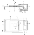
- FIG. 2 is an external perspective view of the power transmission system 401 according to the first embodiment.
- FIG. 3A is a front view of a terminal with a jacket
- FIG. 3B is a side view of the terminal with a jacket placed on the power transmission apparatus 101.
- 4A is a vertical cross-sectional view as viewed from the side of the power transmission apparatus 101
- FIG. 4B is a vertical cross-sectional view as viewed from the side of the terminal with a jacket
- FIG. It is the longitudinal cross-sectional view seen from the side in the state which mounted the terminal.
- FIG. 5 is an equivalent circuit diagram of the power transmission system 401.
- FIG. 6A to 6D are diagrams showing examples of some other structures of the power transmission device side passive electrode 11.
- FIG. 7A is a front view of the power transmission system 402 according to the second embodiment
- FIG. 7B is a longitudinal sectional view seen from the side in a state where a terminal with a jacket is placed on the power transmission apparatus 102.
- FIG. 8 is a simplified circuit diagram of the power transmission system 402.
- FIG. 9 is a longitudinal sectional view seen from the side of the power transmission system 403 of the third embodiment.
- FIG. 10 is a longitudinal sectional view seen from the side of the power transmission system 404 of the fourth embodiment.
- FIG. 11 is a simplified circuit diagram of the power transmission system 404.
- FIG. 2 is an external perspective view of the power transmission system 401 according to the first embodiment.
- the power transmission system 401 includes a power transmission device 101 and a power reception device 301.
- the power receiving device is configured by the terminal 30 and the jacket 201 placed on the outer peripheral frame thereof.
- the terminal 30 (hereinafter referred to as “terminal with jacket”) in a state where the jacket 201 is put on the outer peripheral frame is placed on the power transmission apparatus 101.
- a power receiving circuit is configured in the jacket 201, and the power receiving circuit is connected to the terminal 30 via a connector in the jacket 201.
- FIG. 3A is a front view of the terminal with a jacket
- FIG. 3B is a side view of the terminal with the jacket placed on the power transmission apparatus 101.
- FIG. 3A the lower jacket 201B is slidably attached to the lower part of the terminal 30, and the upper jacket 201T is slidably attached to the upper part of the terminal 30.
- a connector plug 29 is provided inside the lower jacket, and the plug 29 is connected to a receptacle 39 provided at the lower portion of the terminal 30 by attaching the lower jacket 201B to the terminal 30.
- the jacketed terminal is placed so as to be inserted into the groove of the power transmission apparatus 101.
- the jacketed terminal is not limited to being placed vertically but can be placed horizontally, and power can be transmitted in any state.
- FIG. 4A is a vertical cross-sectional view as viewed from the side of the power transmission apparatus 101
- FIG. 4B is a vertical cross-sectional view as viewed from the side of the terminal with a jacket
- FIG. It is the longitudinal cross-sectional view seen from the side in the state which mounted the terminal.
- a power transmission device side passive electrode 11, a power transmission device side active electrode 12, a power transmission module 13, and the like are provided in a casing 15 of the power transmission device 101.
- the power transmission device side active electrode 12 is disposed on the bottom surface of the groove on which the jacketed terminal is placed.
- a part of the power transmission device side passive electrode 11 is exposed at a position in contact with the power reception device side passive electrode 21 slightly protruding from the back surface of the jacket 201B.
- a heat sink portion 11 ⁇ / b> S having a plurality of fins is formed on a part of the power transmission device side passive electrode 11.
- the passive electrode 11 including the heat sink portion 11S is bent and expanded in the housing 15.
- a plurality of slit-like openings 16 for heat dissipation are formed in the casing 15 of the power transmission device 101.
- a power receiving device side passive electrode 21, a power receiving device side active electrode 22, a power receiving module 23, and a DC-DC converter 24 are provided inside a lower jacket 201B which is a part of the power receiving device. It has been.
- the power receiving device side passive electrode 21 is formed so as to surround the power receiving module 23 and the DC-DC converter 24 in the vicinity thereof.
- the power reception apparatus side passive electrode 21 is electrically connected to the power transmission apparatus side passive electrode 11.
- the power receiving device side active electrode 22 faces the power transmitting device side active electrode 12.
- the thickness t3 of the power transmission device side passive electrode 11 is larger than the thickness t1 of the power reception device side passive electrode 21.
- the thickness t4 of the power transmitting device side active electrode 12 is larger than the thickness t2 of the power receiving device side active electrode 22. That is, t3 / t1> 1 t4 / t2> 1 Satisfy the relationship. That is, the heat capacities of the passive electrode and the active electrode on the power transmission device side are larger than the heat capacities of the passive electrode and the active electrode on the power reception device side, and the heat of the power reception device is radiated with high efficiency through the power transmission device.
- the casing 15 and the jacket 201 of the power transmission device 101 are made of a material having high thermal conductivity.
- FIG. 5 is an equivalent circuit diagram of the power transmission system 401.
- the power transmission module 13 of the power transmission apparatus 101 includes a high-frequency voltage generation circuit OSC, a step-up transformer TG, and an inductor LG.
- the high frequency voltage generation circuit OSC generates a high frequency voltage of, for example, 100 kHz to several tens of MHz.
- the booster circuit using the booster transformer TG and the inductor LG boosts the voltage generated by the high-frequency voltage generation circuit OSC and applies it between the passive electrode 11 and the active electrode 12.
- the power transmission module 13 corresponds to the “high frequency high voltage generation circuit” of the present invention.
- the jacket 201 of the power receiving device 301 includes a power receiving module 23, a DC-DC converter 24, and a load circuit RL corresponding to the terminal 30.
- the power receiving module 23 is connected between the active electrode 22 and the passive electrode 21.
- the power receiving module 23 includes an inductor LL, a step-down circuit using a step-down transformer TL, and a rectifier circuit 25 that converts the stepped-down AC voltage into a DC voltage.
- the DC-DC converter 24 outputs a specified DC voltage to the load circuit RL.
- the resistance r connected between the power transmission device side passive electrode 11 and the power reception device side passive electrode 21 corresponds to a contact resistance configured at a contact portion between the power transmission device side passive electrode 11 and the power reception device side passive electrode 21.
- the capacitor Cm connected between the power transmitting device side active electrode 12 and the power receiving device side active electrode 22 corresponds to a capacitance generated between the power transmitting device side active electrode 12 and the power receiving device side active electrode 22.
- the passive electrodes of the power transmission device 101 and the jacket 201 are directly connected to each other, so that the potential of the power reception device side passive electrode 21 becomes substantially equal to the potential of the power transmission device side passive electrode 11.
- the potential of the power receiving device side passive electrode 21 is stabilized, and ground potential fluctuations and leakage of unnecessary electromagnetic fields are suppressed.
- the degree of coupling increases and high transmission efficiency is obtained.
- the power receiving module 23 and the DC-DC converter 24 in particular generate a relatively large amount of heat, but these heat propagates through the power receiving device side passive electrode 21 to the power transmitting device side passive electrode 11. Communicated.
- the power reception device side passive electrode 21 is also electrically connected to the power transmission device side passive electrode 11. Therefore, the heat generated by the power receiving module 23 and the DC-DC converter 24 is dissipated by the power transmitting device side passive electrode 11, and the temperature rise of the power receiving module 23 and the DC-DC converter 24 is suppressed.
- FIGS. 6B and 6C are diagrams showing examples of some other structures of the power transmission device side passive electrode 11.
- the power receiving device side passive electrode 21 is represented by a simple flat plate.
- the power transmitting device side passive electrode 11 may be a simple thick plate without fins.
- a plurality of protrusions may be formed as shown in FIG.
- FIG. 6C a plurality of holes H may be formed inside. If the surface area of the power transmitting device side passive electrode 11 is increased as shown in FIGS. 6B and 6C, the heat dissipation from the power transmitting electrode to the surrounding air is enhanced.
- the power transmission device side active electrode may be one obtained by sticking a plate 11i of a good thermal conductor made of metal or an electrical insulator to a metal plate 11c.
- FIG. 7A is a front view of the power transmission system 402 according to the second embodiment
- FIG. 7B is a longitudinal sectional view seen from the side in a state where a terminal with a jacket is placed on the power transmission apparatus 102.
- a power transmission device-side passive electrode 11, a power transmission device-side active electrode 12, a power transmission device-side detection electrode 17, a power transmission module 13, and the like are provided on the casing 15 of the power transmission device 102. .
- the power receiving device includes a terminal 30 and a jacket 201 attached to the terminal 30.
- the jacket 201 is provided with a power receiving device side passive electrode 21, a power receiving device side active electrode 22, a power receiving module 23, a DC-DC converter 24, and a connector plug 29.
- the power receiving device side passive electrode 21 is formed over at least three surfaces of the outer periphery of the jacket 201 of the power receiving device.
- Other configurations of the power receiving apparatus are the same as those shown in the first embodiment.
- the power transmission device side passive electrode 11 is arranged on the bottom surface of the groove on which the jacketed terminal is placed.
- the power receiving device side passive electrode 21 contacts the power transmitting device side passive electrode 11 in a state where the jacketed terminal is placed in the groove.
- the power transmission device side passive electrode 11 is bent and expanded in the housing 15. In particular, an extended portion 11e in an electrically insulated state and in a thermally coupled state is formed in the vicinity of the power transmission device side detection electrode 17.
- FIG. 8 is a simplified circuit diagram of the power transmission system 402.
- the power reception device side passive electrode 21 is electrically connected to the power transmission device side passive electrode 11 and the power transmission device side detection electrode 17.
- the control circuit 18 detects the presence / absence of electrical continuity between the power transmission device side passive electrode 11 and the detection electrode 17 and invalidates the operation of the power transmission module 13 if the continuity is not established. This eliminates power transmission in an abnormal state without power transmission when the power receiving device (terminal with jacket) is not placed in an appropriate positional relationship with the power transmission device, and therefore power reception due to a decrease in power transmission efficiency. Abnormal overheating of the device and the power transmission device is also suppressed.
- FIG. 9 is a longitudinal sectional view seen from the side of the power transmission system 403 of the third embodiment.
- a power transmission device side passive electrode 11, a power transmission device side active electrode 12, a power transmission module 13, and the like are provided in a casing 15 of the power transmission device 103.
- the power receiving device includes a terminal 30 and a jacket 201 attached to the terminal 30.
- the jacket 201 is provided with a power receiving device side passive electrode 21, a power receiving device side active electrode 22, a power receiving module 23, a DC-DC converter 24, a shield plate 28, and the like.
- Other basic configurations of the power receiving apparatus are the same as those shown in the first and second embodiments.
- the power transmission device side passive electrode 11 is disposed on the bottom surface of the mounting table on which the jacketed terminal is mounted. In a state where the terminal with the jacket is placed on the placing table, the power receiving device side passive electrode 21 contacts the power transmitting device side passive electrode 11.
- the periphery of the power transmission module 13 of the power transmission apparatus 103 is surrounded by a shield case 19.
- the shield case 19 is electrically connected to the power transmission device side passive electrode 11 via the wiring conductor 14.
- the shield plate 28 of the power receiving apparatus is disposed close to the power receiving module 23 and the DC-DC converter 24, and is electrically shielded and thermally coupled. And this shield board 28 is arrange
- the heat of the power receiving module 23 and the DC-DC converter 24 of the power receiving device is radiated at the power transmitting device side passive electrode 11 through the shield plate 28 and through the power receiving device side passive electrode 21.
- FIG. 10 is a longitudinal sectional view seen from the side of the power transmission system 404 of the fourth embodiment.
- a power transmission device side passive electrode 11, a power transmission device side active electrode 12, a power transmission device side detection electrode, a power transmission module 13, and the like are provided in a casing 15 of the power transmission device 104.
- the power receiving device includes a terminal 30 and a jacket 201 attached to the terminal 30.
- the jacket 201 is provided with a power receiving device side passive electrode 21, a power receiving device side active electrode 22, a power receiving module 23, a DC-DC converter 24, and the like.
- Other basic configurations of the power receiving apparatus are the same as those shown in the first and second embodiments.
- the power transmission device side passive electrode 11 is formed and arranged along the power reception device side passive electrode 21 so as to face the power reception device side passive electrode 21. In a state in which the jacketed terminal is placed on the mounting table, the power receiving device side passive electrode 21 faces the power transmitting device side passive electrode 11.
- the power transmission device side passive electrode 11 Since the power transmission device side passive electrode 11 is expanded in the casing 15 in a direction away from the power reception device side passive electrode 21, the power reception device has a coupling capacitance or stray capacitance between the passive electrode 21 and the power transmission device side passive electrode 11.
- the volume and surface area of the power transmission device side passive electrode 11 can be increased without changing (without adverse effects).
- FIG. 11 is a simplified circuit diagram of the power transmission system 404.
- the power reception device side passive electrode 21 faces the power transmission device side passive electrode 11 and the power transmission device side detection electrode 17.
- the power receiving device side active electrode 22 faces the power transmitting device side active electrode 12.
- the fourth embodiment is an example in which the passive electrodes of the power transmission device and the power reception device and the active electrodes are electrically coupled to each other, and power is transmitted from the power transmission device 104 to the power reception device 304.
- the control circuit 18 detects the magnitude of the capacitance between the power transmission device side passive electrode 11 and the detection electrode 17, and invalidates the operation of the power transmission module 13 if the capacitance is smaller than the threshold value.
- the power receiving device side passive electrode 21 when there are a plurality of electrodes opposed to the power receiving device side passive electrode 21 on the power transmitting device side, if the heat capacity of these electrodes is increased and thermal coupling with the power receiving device side passive electrode 21 is achieved, the power receiving device Since the heat transfer efficiency from the power transmission device to the power transmission device increases, the heat dissipation effect of the power transmission device side passive electrode 11 increases.
- the heat of the power receiving device is dissipated with high efficiency via the power transmitting device, so that the temperature rise of the power receiving device can be suppressed.
Landscapes
- Engineering & Computer Science (AREA)
- Power Engineering (AREA)
- Computer Networks & Wireless Communication (AREA)
- Electric Propulsion And Braking For Vehicles (AREA)
- Charge And Discharge Circuits For Batteries Or The Like (AREA)
- Cooling Or The Like Of Electrical Apparatus (AREA)
- Current-Collector Devices For Electrically Propelled Vehicles (AREA)
Abstract
Priority Applications (4)
| Application Number | Priority Date | Filing Date | Title |
|---|---|---|---|
| DE112012002474.5T DE112012002474T5 (de) | 2011-06-14 | 2012-05-21 | Energieübertragungsvorrichtung und Energieübertragungssytem |
| CN201280003679.9A CN103222153B (zh) | 2011-06-14 | 2012-05-21 | 供电装置以及电力输送系统 |
| JP2012558121A JP5376071B2 (ja) | 2011-06-14 | 2012-05-21 | 送電装置および電力伝送システム |
| US13/868,659 US9369009B2 (en) | 2011-06-14 | 2013-04-23 | Power transmitting device and power transmission system |
Applications Claiming Priority (2)
| Application Number | Priority Date | Filing Date | Title |
|---|---|---|---|
| JP2011-132289 | 2011-06-14 | ||
| JP2011132289 | 2011-06-14 |
Related Child Applications (1)
| Application Number | Title | Priority Date | Filing Date |
|---|---|---|---|
| US13/868,659 Continuation US9369009B2 (en) | 2011-06-14 | 2013-04-23 | Power transmitting device and power transmission system |
Publications (1)
| Publication Number | Publication Date |
|---|---|
| WO2012172930A1 true WO2012172930A1 (fr) | 2012-12-20 |
Family
ID=47356924
Family Applications (1)
| Application Number | Title | Priority Date | Filing Date |
|---|---|---|---|
| PCT/JP2012/062903 Ceased WO2012172930A1 (fr) | 2011-06-14 | 2012-05-21 | Dispositif d'émission d'énergie électrique et système de réception d'énergie électrique |
Country Status (5)
| Country | Link |
|---|---|
| US (1) | US9369009B2 (fr) |
| JP (1) | JP5376071B2 (fr) |
| CN (1) | CN103222153B (fr) |
| DE (1) | DE112012002474T5 (fr) |
| WO (1) | WO2012172930A1 (fr) |
Cited By (1)
| Publication number | Priority date | Publication date | Assignee | Title |
|---|---|---|---|---|
| WO2014112639A1 (fr) * | 2013-01-21 | 2014-07-24 | 株式会社村田製作所 | Système d'émission de puissance |
Families Citing this family (8)
| Publication number | Priority date | Publication date | Assignee | Title |
|---|---|---|---|---|
| WO2014196384A1 (fr) * | 2013-06-06 | 2014-12-11 | 株式会社村田製作所 | Dispositif et procédé d'inspection de système de transmission de puissance sans contact |
| US11228207B2 (en) * | 2014-04-02 | 2022-01-18 | Sony Group Corporation | Power receiving device, control method thereof, and feed system |
| US10312731B2 (en) * | 2014-04-24 | 2019-06-04 | Westrock Shared Services, Llc | Powered shelf system for inductively powering electrical components of consumer product packages |
| US20170129344A1 (en) * | 2015-11-06 | 2017-05-11 | Qualcomm Incorporated | Methods and apparatus for thermal dissipation in vehicle pads for wireless power transfer applications |
| US20180351402A1 (en) | 2015-12-01 | 2018-12-06 | Philips Lighting Holding B.V. | Capacitive power transfer arrangement |
| JP6663725B2 (ja) * | 2016-01-19 | 2020-03-13 | 東芝テック株式会社 | 非接触電力送電装置及び電力送受電装置 |
| US11139690B2 (en) * | 2018-09-21 | 2021-10-05 | Solace Power Inc. | Wireless power transfer system and method thereof |
| CN118648220A (zh) * | 2023-01-12 | 2024-09-13 | 华为数字能源技术有限公司 | 无线充电设备、电子终端设备及无线充电系统 |
Citations (2)
| Publication number | Priority date | Publication date | Assignee | Title |
|---|---|---|---|---|
| WO2011040392A1 (fr) * | 2009-09-29 | 2011-04-07 | 国立大学法人 電気通信大学 | Dispositif, système et procédé de transmission d'énergie électrique et d'informations |
| JP2011083132A (ja) * | 2009-10-07 | 2011-04-21 | Takenaka Komuten Co Ltd | 電力供給システム |
Family Cites Families (4)
| Publication number | Priority date | Publication date | Assignee | Title |
|---|---|---|---|---|
| CN101416411B (zh) | 2006-03-21 | 2013-05-15 | 株式会社村田制作所 | 通过穿越电介质的局部感应传输能量的装置 |
| JP2009089520A (ja) | 2007-09-28 | 2009-04-23 | Takenaka Komuten Co Ltd | 電力供給システム |
| JP4557049B2 (ja) | 2008-06-09 | 2010-10-06 | ソニー株式会社 | 伝送システム、給電装置、受電装置、及び伝送方法 |
| US8497659B2 (en) * | 2010-03-23 | 2013-07-30 | Nyko Technologies, Inc. | Video game controller charging system |
-
2012
- 2012-05-21 WO PCT/JP2012/062903 patent/WO2012172930A1/fr not_active Ceased
- 2012-05-21 JP JP2012558121A patent/JP5376071B2/ja not_active Expired - Fee Related
- 2012-05-21 DE DE112012002474.5T patent/DE112012002474T5/de not_active Withdrawn
- 2012-05-21 CN CN201280003679.9A patent/CN103222153B/zh not_active Expired - Fee Related
-
2013
- 2013-04-23 US US13/868,659 patent/US9369009B2/en not_active Expired - Fee Related
Patent Citations (2)
| Publication number | Priority date | Publication date | Assignee | Title |
|---|---|---|---|---|
| WO2011040392A1 (fr) * | 2009-09-29 | 2011-04-07 | 国立大学法人 電気通信大学 | Dispositif, système et procédé de transmission d'énergie électrique et d'informations |
| JP2011083132A (ja) * | 2009-10-07 | 2011-04-21 | Takenaka Komuten Co Ltd | 電力供給システム |
Cited By (2)
| Publication number | Priority date | Publication date | Assignee | Title |
|---|---|---|---|---|
| WO2014112639A1 (fr) * | 2013-01-21 | 2014-07-24 | 株式会社村田製作所 | Système d'émission de puissance |
| US10014720B2 (en) | 2013-01-21 | 2018-07-03 | Murata Manufacturing Co., Ltd. | Power transmission system |
Also Published As
| Publication number | Publication date |
|---|---|
| CN103222153B (zh) | 2015-03-25 |
| US9369009B2 (en) | 2016-06-14 |
| DE112012002474T5 (de) | 2014-02-27 |
| CN103222153A (zh) | 2013-07-24 |
| US20130270922A1 (en) | 2013-10-17 |
| JP5376071B2 (ja) | 2013-12-25 |
| JPWO2012172930A1 (ja) | 2015-02-23 |
Similar Documents
| Publication | Publication Date | Title |
|---|---|---|
| JP5376071B2 (ja) | 送電装置および電力伝送システム | |
| JP5168438B2 (ja) | 電力伝送システム、及び受電ジャケット | |
| JP5403073B2 (ja) | 電力受電装置及び電力送電装置 | |
| US10660243B2 (en) | Power conversion apparatus including a heat-dissipation module | |
| US20190035543A1 (en) | Coil unit, and power transmitting device, power receiving device and wireless power transmission system using the coil unit | |
| US10804709B2 (en) | Coil unit, and power transmitting device, power receiving device and wireless power transmission system using the coil unit | |
| US20150372505A1 (en) | Power transmission device and power reception device | |
| JPWO2017022221A1 (ja) | 放熱構造および電子機器 | |
| JP5874844B2 (ja) | ワイヤレス電力伝送システム | |
| JP2013150414A (ja) | トランス及びスイッチング電源装置 | |
| JP2016006848A (ja) | トランスモジュール及び受電装置 | |
| JP6582717B2 (ja) | 電子電気機器 | |
| JP6379353B2 (ja) | Dc−dcコンバータ | |
| JP2011187729A (ja) | 電界放射低減構造 | |
| JP2016119395A (ja) | 電源装置 | |
| CN108418282A (zh) | 无线充电器结构 | |
| CN104769826B (zh) | 电连接组件 | |
| KR20120055345A (ko) | 전원공급장치 | |
| KR20160139218A (ko) | 디씨-디씨 컨버터 | |
| CN222356768U (zh) | 一种电源适配器 | |
| JP2017034029A (ja) | 共振器 | |
| JP2008041398A (ja) | マイクロ波発生装置およびマイクロ波処理装置 | |
| TWI565399B (zh) | Anti - electromagnetic interference structure of wireless power transmission device | |
| JP5156140B1 (ja) | 通信装置 | |
| JP2016082745A (ja) | 電源装置 |
Legal Events
| Date | Code | Title | Description |
|---|---|---|---|
| ENP | Entry into the national phase |
Ref document number: 2012558121 Country of ref document: JP Kind code of ref document: A |
|
| 121 | Ep: the epo has been informed by wipo that ep was designated in this application |
Ref document number: 12800811 Country of ref document: EP Kind code of ref document: A1 |
|
| WWE | Wipo information: entry into national phase |
Ref document number: 1120120024745 Country of ref document: DE Ref document number: 112012002474 Country of ref document: DE |
|
| 122 | Ep: pct application non-entry in european phase |
Ref document number: 12800811 Country of ref document: EP Kind code of ref document: A1 |