WO2012176247A1 - プリント基板 - Google Patents
プリント基板 Download PDFInfo
- Publication number
- WO2012176247A1 WO2012176247A1 PCT/JP2011/005151 JP2011005151W WO2012176247A1 WO 2012176247 A1 WO2012176247 A1 WO 2012176247A1 JP 2011005151 W JP2011005151 W JP 2011005151W WO 2012176247 A1 WO2012176247 A1 WO 2012176247A1
- Authority
- WO
- WIPO (PCT)
- Prior art keywords
- land
- solder
- row
- lands
- circuit board
- Prior art date
- Legal status (The legal status is an assumption and is not a legal conclusion. Google has not performed a legal analysis and makes no representation as to the accuracy of the status listed.)
- Ceased
Links
Images




Classifications
-
- H—ELECTRICITY
- H05—ELECTRIC TECHNIQUES NOT OTHERWISE PROVIDED FOR
- H05K—PRINTED CIRCUITS; CASINGS OR CONSTRUCTIONAL DETAILS OF ELECTRIC APPARATUS; MANUFACTURE OF ASSEMBLAGES OF ELECTRICAL COMPONENTS
- H05K3/00—Apparatus or processes for manufacturing printed circuits
- H05K3/30—Assembling printed circuits with electric components, e.g. with resistors
- H05K3/32—Assembling printed circuits with electric components, e.g. with resistors electrically connecting electric components or wires to printed circuits
- H05K3/34—Assembling printed circuits with electric components, e.g. with resistors electrically connecting electric components or wires to printed circuits by soldering
- H05K3/3447—Lead-in-hole components
-
- H—ELECTRICITY
- H05—ELECTRIC TECHNIQUES NOT OTHERWISE PROVIDED FOR
- H05K—PRINTED CIRCUITS; CASINGS OR CONSTRUCTIONAL DETAILS OF ELECTRIC APPARATUS; MANUFACTURE OF ASSEMBLAGES OF ELECTRICAL COMPONENTS
- H05K1/00—Printed circuits
- H05K1/02—Details
- H05K1/11—Printed elements for providing electric connections to or between printed circuits
- H05K1/115—Via connections; Lands around holes or via connections
- H05K1/116—Lands, clearance holes or other lay-out details concerning the surrounding of a via
-
- H—ELECTRICITY
- H05—ELECTRIC TECHNIQUES NOT OTHERWISE PROVIDED FOR
- H05K—PRINTED CIRCUITS; CASINGS OR CONSTRUCTIONAL DETAILS OF ELECTRIC APPARATUS; MANUFACTURE OF ASSEMBLAGES OF ELECTRICAL COMPONENTS
- H05K2201/00—Indexing scheme relating to printed circuits covered by H05K1/00
- H05K2201/09—Shape and layout
- H05K2201/09209—Shape and layout details of conductors
- H05K2201/09372—Pads and lands
- H05K2201/09381—Shape of non-curved single flat metallic pad, land or exposed part thereof; Shape of electrode of leadless component
-
- H—ELECTRICITY
- H05—ELECTRIC TECHNIQUES NOT OTHERWISE PROVIDED FOR
- H05K—PRINTED CIRCUITS; CASINGS OR CONSTRUCTIONAL DETAILS OF ELECTRIC APPARATUS; MANUFACTURE OF ASSEMBLAGES OF ELECTRICAL COMPONENTS
- H05K2201/00—Indexing scheme relating to printed circuits covered by H05K1/00
- H05K2201/09—Shape and layout
- H05K2201/09209—Shape and layout details of conductors
- H05K2201/09654—Shape and layout details of conductors covering at least two types of conductors provided for in H05K2201/09218 - H05K2201/095
- H05K2201/09781—Dummy conductors, i.e. not used for normal transport of current; Dummy electrodes of components
-
- H—ELECTRICITY
- H05—ELECTRIC TECHNIQUES NOT OTHERWISE PROVIDED FOR
- H05K—PRINTED CIRCUITS; CASINGS OR CONSTRUCTIONAL DETAILS OF ELECTRIC APPARATUS; MANUFACTURE OF ASSEMBLAGES OF ELECTRICAL COMPONENTS
- H05K2201/00—Indexing scheme relating to printed circuits covered by H05K1/00
- H05K2201/10—Details of components or other objects attached to or integrated in a printed circuit board
- H05K2201/10227—Other objects, e.g. metallic pieces
- H05K2201/10295—Metallic connector elements partly mounted in a hole of the PCB
- H05K2201/10303—Pin-in-hole mounted pins
-
- H—ELECTRICITY
- H05—ELECTRIC TECHNIQUES NOT OTHERWISE PROVIDED FOR
- H05K—PRINTED CIRCUITS; CASINGS OR CONSTRUCTIONAL DETAILS OF ELECTRIC APPARATUS; MANUFACTURE OF ASSEMBLAGES OF ELECTRICAL COMPONENTS
- H05K2201/00—Indexing scheme relating to printed circuits covered by H05K1/00
- H05K2201/10—Details of components or other objects attached to or integrated in a printed circuit board
- H05K2201/10227—Other objects, e.g. metallic pieces
- H05K2201/10424—Frame holders
-
- H—ELECTRICITY
- H05—ELECTRIC TECHNIQUES NOT OTHERWISE PROVIDED FOR
- H05K—PRINTED CIRCUITS; CASINGS OR CONSTRUCTIONAL DETAILS OF ELECTRIC APPARATUS; MANUFACTURE OF ASSEMBLAGES OF ELECTRICAL COMPONENTS
- H05K2203/00—Indexing scheme relating to apparatus or processes for manufacturing printed circuits covered by H05K3/00
- H05K2203/04—Soldering or other types of metallurgic bonding
- H05K2203/046—Means for drawing solder, e.g. for removing excess solder from pads
Definitions
- the present invention relates to a printed circuit board in which a lead portion of a mounting component is inserted and soldered to a land portion provided in a through hole.
- the heating iron portion of the soldering apparatus is continuously moved while being moved in the alignment direction of the through holes.
- the lead portions be soldered to a plurality of land portions, that is, be performed by so-called drag solder.
- drag solder the one described in JP-A-2005-294480 (Patent Document 1) is that. According to such a pulling solder, since continuous soldering to a plurality of land portions becomes possible, the working time is longer than so-called robot soldering in which soldering is performed with a soldering apparatus for each land portion. Can be significantly shortened.
- the soldering iron portion is moved on one land row to perform continuous soldering.
- solder balls are formed, and the solder balls may cause damage or failure of the printed circuit board or other mounted components.
- the present invention has been made against the background described above, and the problem to be solved is a print of a novel structure in which a plurality of land rows separated from one another can be drawn and soldered successively. It is in providing a substrate.
- a plurality of land portions provided in through holes are aligned, and lead portions of mounting components are inserted through the through holes of the plurality of land portions, and the land portions are formed.
- a first land row composed of a group of the plurality of aligned lands and a group of the plurality of aligned lands in the printed circuit board on which the lead portions are soldered by pull soldering.
- the second land row composed of the first and second land rows is disposed apart from each other, while the end of the first land row on the end point side of the pulling solder and the starting point side of the second land row on the pulling solder And an intermediate dummy land portion extending between the end portion and the second end portion.
- the intermediate dummy land portion extending between the end side end of the first land row and the start side end of the second land row is provided, When soldering is performed and the heating iron portion is moved from the first land row to the second land row, the heating iron portion can be moved by sliding on the intermediate dummy land portion. Therefore, since it is not necessary to once pull up the heating iron portion on the printed circuit board and move it to the second land row, the workability of the soldering by pulling solder can be improved.
- the heating iron can be placed on the intermediate dummy land and moved along the intermediate dummy land, the excess solder is absorbed into the intermediate dummy land while the heating iron of the heating iron.
- the heating temperature and the required amount of solder can be stably maintained, and problems such as formation of a solder bridge on the end side of the first land row and lack of solder on the start side of the second land row can be generated. It can be advantageously prevented.
- the intermediate dummy land portion may extend between the end side end of the first land row and the start side end of the second land row, and may extend linearly between them, It includes anything that extends in a bent or curved manner.
- the first land row and the second land row are spaced apart from each other in a straight line in the alignment direction of the plurality of land portions.
- the intermediate dummy land portions extending in the alignment direction are provided between the first land row and the second land row while being aligned.
- the intermediate dummy land portions provided between the first land row and the second land row aligned in a straight line extend linearly in the alignment direction. Therefore, the first land row and the second land row can be soldered continuously only by moving the heating soldering iron portion along the straight line in pulling solder, and one layer of pulling solder operation Stabilization and efficiency.
- the end of the intermediate dummy land portion on the first land row side extends in the extending direction of the intermediate dummy land portion.
- Extension lands extending to both sides in the cross direction are provided in a connected manner.
- the extension land portion of the intermediate dummy land portion is provided adjacent to the end on the end point side of the first row of lands in which the excess solder tends to be a problem. Therefore, when soldering of the first land row is completed, the heating iron can be moved to the intermediate dummy land and the excess solder can be absorbed quickly by the extending land.
- the extending land portion extends in the extending direction of the intermediate dummy land portion, that is, in the movement direction of the heating iron portion, it is brought into contact with the heating iron portion to be heated. It will be. As a result, the excess solder in contact with the extended land portion is maintained at a relatively high temperature, and the excess solder can be quickly absorbed into the extended land portion.
- the land portion and the lead portion are soldered by the pulling solder using lead-free solder. It is a thing.
- the first land row and the second land row can be soldered continuously by sliding and moving the intermediate dummy land portion without pulling up the heating iron portion from the printed board It is possible to stabilize the heating state of the trowel portion and the solder supply state. Therefore, even when lead-free solder having a high melting point is used, the first land row and the second land row can be continuously drawn and soldered in a stable state.
- the intermediate dummy land portion extending between the end side end of the first land row and the start side end of the second land row is provided, the intermediate dummy land portion is interposed.
- the soldering by pulling solder can be performed continuously from the start side end of the first land row to the end side end of the second land row, and the workability of the soldering can be improved.
- the heating iron can be placed on the intermediate dummy land and moved along the intermediate dummy land, the necessary amount of solder can be absorbed while the excess solder is absorbed into the intermediate dummy land. It can be stably maintained, and defects such as formation of solder bridges between each land row and the intermediate dummy land portion can be advantageously prevented.
- the principal part expansion disassembled perspective view which shows the surface side of the printed circuit board as one Embodiment of this invention.
- the principal part enlarged plan view which shows the back surface side of the printed circuit board shown in FIG.
- the enlarged plan view showing an example of the land part which constitutes the printed circuit board concerning the present invention.
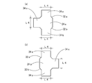
- the example of the dummy land part which comprises the printed circuit board which concerns on this invention is shown, (a) is an enlarged plan view of the dummy land part of one end side in the land alignment direction, (b) is the dummy land part of the other end side in the land alignment direction.
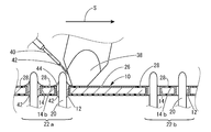
- FIG. 6 is an enlarged cross-sectional view showing a state of a pull solder using land portions and intermediate dummy land portions constituting the printed circuit board according to the present invention, and a view corresponding to the VI-VI cross-sectional view of FIG.
- FIG. 7 is an enlarged cross-sectional view showing a state of a pull solder using a land portion constituting a printed circuit board according to the present invention, and a view corresponding to a VII-VII cross-sectional view of FIG. 2;
- FIG. 10 is an enlarged plan view showing another example of the intermediate dummy land portion that constitutes the printed circuit board according to the present invention.
- the printed circuit board 10 is a substantially rectangular flat substrate surface formed of a known insulating material, in which printed wiring (not shown) is formed.
- a plurality of through holes 12 aligned along the side edge are formed through the side edge of the printed circuit board 10.
- a land portion 14 made of a conductor such as copper foil is integrally formed over the inner peripheral surface of each through hole 12 and the opening peripheral edge on the front surface side and the back surface side of the printed circuit board 10. It is electrically connected.
- the surface land part 14a which comprises the land part 14 is shown by FIG. 1
- the back surface land part 14b which comprises the land part 14 is shown by FIG.
- the mounted components 16 a and 16 b such as connectors mounted on the printed circuit board 10 have a plurality of lead portions 20 fixed through to the resin pedestal 18, and the tip portions of these lead portions 20 are the surface of the printed circuit board 10.
- the resin pedestal 18 is mounted on the printed circuit board 10 in a state where the resin pedestal 18 is inserted into the through hole 12 from the side and projected to the back side of the printed circuit board 10. Then, the plurality of lead portions 20 and the land portions 14 are drawn and soldered from the back surface side of the printed circuit board 10 so that the mounted components 16 a and 16 b are mounted on the printed circuit board 10.
- a first land row 22a through which the lead portion 20 of the mounting component 16a is inserted and a lead portion 20 of the mounting component 16b.
- the second land rows 22b to be inserted are arranged on a straight line, separated from each other in the alignment direction of the land portions 14.
- Each land row 22a, 22b is formed of a plurality of lands 14 provided in the through holes 12 and aligned in a group.
- the dummy land portions 24a and 24b are adjacent to the rear surface land portions 14b on the outer side in the alignment direction of the rear surface land portions 14b located on both ends. Each is provided.
- an intermediate dummy land portion 26 extending in the alignment direction is provided between the first land row 22a and the second land row 22b. .
- the periphery of each rear surface land portion 14b, the dummy land portions 24a and 24b, and the intermediate dummy land portion 26 is covered with a known solder resist layer 28.
- FIG. 3 shows an enlarged plan view of the rear surface land portion 14b.
- the rear surface land portion 14b has a substantially rectangular outer shape in plan view, and extends on both sides in a direction (vertical direction in FIG. 3) orthogonal to the alignment direction (horizontal direction in FIG. 3) of the rear surface land portion 14b.
- a pair of extending land portions 30a and 30b are provided in a connected manner.
- the extended land portions 30a and 30b extend with a substantially constant width dimension, and have a substantially rectangular outer shape in a plan view.
- the throttling portions 32a and 32b are provided at the connecting portions of the rear surface land portion 14b and the extending land portions 30a and 30b.
- the narrowed portions 32a and 32b are such that the length dimension in the alignment direction (left and right direction in FIG. 3) of the back surface lands 14b is gradually reduced outward in the extending direction of the extending lands 30a and 30b.
- the minimum length dimension: L2 is set larger than the outer diameter of the through hole 12: L1.
- the extended land portions 30a and 30b extend outward while maintaining the minimum length dimension L2 of the narrowed portions 32a and 32b.
- the length dimension L3 from the outer edge of the through hole 12 to the extension end of the extending land portions 30a and 30b is equal to or larger than the external dimension L1 of the through hole 12.
- FIGS. 4A and 4B show enlarged plan views of the dummy lands 24a and 24b.
- the dummy lands 24a and 24b have a substantially rectangular outer shape in a plan view, similarly to the rear surface land 14b. Since the dummy lands 24 a and 24 b are not connected to the leads 20 of the mounted components, the through holes 12 are not provided.
- the dummy lands 24a and 24b have a pair of extension lands 34a, which extend on both sides in the direction (vertical direction in FIG. 4) orthogonal to the left and right direction in FIG. 34b are provided in connection.
- the same narrowed portions 32a and 32b as those of the back surface land 14b are provided.
- the extending land portions 34a and 34b extend outward while maintaining the length dimension L4 (left and right direction in FIG. 4) reduced by the narrowed portions 32a and 32b, and are substantially rectangular in plan view. It has an outer shape.
- the length dimension L4 of the extended land portions 34a and 34b is set to be substantially the same as the length dimension L2 of the extended land portions 30a and 30b of the back surface land portion 14b.
- a back surface land of an end portion (left end in FIG. 2) which is a starting point in soldering with pulling solder described later
- An extension land 34c extending outward in the alignment direction (left side in FIGS. 2 and 4) is provided on the dummy land 24a provided adjacent to the outer side in the alignment direction of 14b via the narrowed portions 32a and 32b. It is connected.
- FIG. 4B in the alignment direction of the back surface lands 14b of the second land row 22b, the back surface of the end portion (right end in FIG.
- an extension land portion 34c extending outward in the alignment direction (right side in FIGS. 2 and 4) has the narrowed portions 32a and 32b. It is connected via.
- Each of the extended land portions 34c, 34c maintains the length dimension L4 (vertical direction in FIG. 4) reduced by the narrowed portions 32a, 32b, and becomes outward in the alignment direction of the back surface land portion 14b. 4 and each have a substantially rectangular outer shape in plan view.
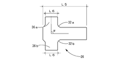
- the intermediate dummy land portion 26 extend along the alignment direction between the end of the first land row 22 a on the end point side of the lead solder and the end of the second land row 22 b on the start side of the lead solder. In plan view, it has an outer shape substantially rectangular in a plan view. Since the intermediate dummy land portion 26 is not connected to the lead portion 20 of the mounted component, the through holes 12 are not provided as in the case of the dummy land portions 24a and 24b.
- the length dimension L5 of the intermediate dummy land portion 26 can be set arbitrarily, but preferably, as shown in FIG. 2, between adjacent back surface land portions 14b in the alignment direction of the back surface land portions 14b It is preferable that the same clearance dimension: w be on both sides, and the length be extended over the entire length between the first land row 22a and the second land row 22b.
- the intermediate dummy land portion 26 at the end on the first land row 22a side, in the direction (vertical direction in FIG. 5) intersecting the left and right direction in FIG. 5, which is the extending direction of the intermediate dummy land portion 26.
- a pair of extending land portions 36a and 36b extending to both sides are provided in a connected manner.
- the crossing angle ⁇ of the back lands 14b of the extension lands 36a and 36b with respect to the alignment direction is preferably 30 ° to 150 °, similarly to the extension lands 30a and 30b provided on the back lands 14b.
- the angle is more preferably 60 ° to 120 °, and still more preferably 90 ° (orthogonal).
- the crossing angle ⁇ is 150 ° or more, the surface tension does not sufficiently act on the solder between the end portion on the first land row 22a side, and the solder is not divided properly and a solder bridge is formed.
- the crossing angle ⁇ becomes 30 ° or less, the separation distance between the end on the first land row 22a side and the intermediate dummy land portion 26 becomes large, and the solder falls onto the printed circuit board 10
- the crossing angle ⁇ of the extension lands 36 a and 36 b in the extension direction with respect to the alignment direction of the back surface lands 14 b is 90 °, and the solder attached to the extension lands 36 a and 36 b And the solder attached to the end of the first land row 22a on the end point side is appropriately secured.
- the same narrowed portions 32a and 32b as those of the back surface land portion 14b are provided.
- the extending land portions 36a and 36b extend outward while maintaining the length dimension L6 (left and right direction in FIG. 5) reduced by the narrowed portions 32a and 32b, and are substantially rectangular in plan view. It has an outer shape.
- the length dimension L6 of the extension lands 36a and 36b is set to be substantially the same as the length dimension L2 of the extension lands 30a and 30b connected to the rear surface land 14b. There is.
- FIGS. 6 and 7. 6 schematically shows how pulling solder is performed on the printed circuit board 10 shown in FIG. 2, and is a view corresponding to the VI-VI cross-sectional view of FIG.
- soldering apparatus Prior to soldering, power is supplied to a soldering apparatus (not shown), and the heating iron 38 is heated to a degree sufficient to melt the thread-like solder 42 supplied from the solder supply unit 40. Ru.
- lead-free solder is employed as the solder 42.
- the heating iron 38 is moved in the moving direction indicated by the arrow S in FIG. 6, that is, from the left side to the right in FIG. It will be soldered continuously.
- the temperature and moving speed of the soldering iron portion 38, the amount of supplied solder, and the like are appropriately set so that the molten solder 42 is appropriately divided between the land portions 14 so that the solder fillets 44 described later are favorably formed. It has been adjusted.
- the heating iron portion 38 whose heating has been completed is first placed on the dummy land portion 24a provided adjacent to the back surface land portion 14b located at the end of the first land row 22a, and the solder supply portion A proper amount of solder 42 supplied from 40 is melted and stands by on the dummy land portion 24 a until it becomes a soldering start state to reach the end of the heating iron portion 38.
- solder fillets 44 are formed. As a result, each land portion 14 is soldered to each lead portion 20.
- the heating iron portion 38 supplies the solder 42 to each land portion 14 and passes through the first land row 22 a while moving in the movement direction from the dummy land portion 24 a on the starting point side. Thereafter, as shown in FIG. 6, the heating iron 38 is between the end of the first land row 22a on the end point side of the pulling solder and the end of the second land row 22b on the starting point side of the pulling solder.
- the extended intermediate dummy land portion 26 is reached.
- the land rows 22a and 22b and the intermediate dummy lands 26 are aligned on a straight line, the movement direction and movement speed of the heating iron 38 are continuously maintained in a constant state. Soldering is performed.
- the heating iron portion 38 passes through the second land row 22b after passing through the intermediate dummy land portion 26, and then reaches the dummy land portion 24b on the end point side to complete the pulling solder.
- the through holes 12 are formed by the solder 42 melted from the heating iron 38.
- each land portion 14 is soldered to each lead portion 20.
- the heating iron 38 which has passed through the second land row 22b is finally placed on the dummy land 24b provided adjacent to the back surface land 14b located at the end of the second land row 22b. After the soldering is completed, the printed circuit board 10 is pulled up.
- FIG. 7 shows a state of the drawn solder in a direction orthogonal to the moving direction of the heating iron portion 38, and is a view corresponding to the VII-VII sectional view of FIG.
- the heating iron portion 38 is provided with a distal end recessed groove 46 into which the lead portion 20 can be inserted. Therefore, since the lead portion 20 can pass through the end recessed groove 46 when performing the pulling solder, the interference between the lead portion 20 and the heating iron portion 38 is avoided when the heating iron portion 38 moves. It has become.
- extending land portions 30a and 30b are provided so as to extend in a direction (left and right direction in FIG. 7) orthogonal to the alignment direction of the back surface land portions 14b. That is, since the extending land portions 30a and 30b are provided on the moving path of the heating iron portion 38 at the time of pulling solder, the tip end face of the heating iron portion 38 at the time of pulling solder extends this It abuts on the lands 30a and 30b. Therefore, the extension lands 30a and 30b are heated by the heating iron 38.
- the extension lands 30a and 30b extend with a length dimension L3 that is equal to or greater than the outer diameter dimension of the through hole 12, and sufficient for the entire area of the tip surface of the heating iron 38 to abut. It is considered to be large.
- the solder 42 is absorbed over substantially the entire extension land portions 30a, 30b, and the solder fillet 44 is expanded and spread larger than the alignment direction shown in FIG. It is formed.
- the pair of extension lands 34 a and 34 b provided on the dummy lands 24 a and 24 b and the pair of extension lands 36 a and 36 b provided on the intermediate dummy land 26 are also included. Since the back surface lands 14b extend in a direction (left and right direction in FIG. 7) orthogonal to the alignment direction, the tips of the heating irons 38 also move when the heating irons 38 move. It will be in contact with the surface to be heated.
- the intermediate dummy land portion 26 extending between the end side end of the first land row 22a and the start side end of the second land row 22b. Can be drawn continuously from the start end of the first land row 22a to the end end of the second land row 22b via the intermediate dummy land portion 26. . Therefore, work such as temporarily interrupting the pulling solder between the first land row 22a and the second land row 22b, pulling up the heating iron 38 on the printed circuit board 10 and moving it to the second land row 22b It becomes unnecessary, and the workability of the soldering by pull soldering can be improved.
- the heating iron 38 can be placed on the intermediate dummy land 26 and moved along the extension direction of the intermediate dummy land 26, the excess solder is absorbed into the intermediate dummy land 26. While the heating temperature of the soldering iron 38 and the required amount of solder can be stably maintained, the formation of the solder bridge on the end point side of the first land row 22a and the starting point of the second land row 22b It is possible to advantageously prevent the occurrence of problems such as insufficient solder on the side.
- the intermediate dummy land portion 26 is provided between the first land row 22a and the second land row 22b, and these are aligned in a straight line,
- the first land row 22a and the second land row 22b can be soldered continuously by only a simple operation of moving the heating iron portion 38 linearly along the alignment direction of the land portions 14; It is possible to achieve further stabilization and efficiency of the work of pulling solder.
- the extension land portions 36a and 36b of the intermediate dummy land portion 26 are provided adjacent to the end portion of the first land row 22a on the end point side where excess solder tends to be a problem. Therefore, when soldering of the first land row 22a is finished, the heating iron 38 is moved to the intermediate dummy land 26 and the excess lands are quickly absorbed by the extended lands 36a and 36b. it can.
- the extending land portions 36 a and 36 b extend orthogonal to the extending direction of the intermediate dummy land portion 26, that is, the moving direction of the heating iron portion 38, the extending land portions 36 a and 36 b correspond to the heating iron portion 38. It will be touched and heated. As a result, the excess solder in contact with the extended land portions 36a and 36b can be maintained at a relatively high temperature, and the excess solder can be quickly absorbed into the extended land portions 36a and 36b.
- the heating iron 38 when moving from the first land row 22a to the second land row 22b, the heating iron 38 is slid over the intermediate dummy lands 26 without interrupting the pulling solder operation, and the first land row 22a Since the soldering can be continuously performed from the starting point side end to the end side end of the second land row 22b, the heating state and the solder supply state of the heating iron portion 38 can be stabilized. Therefore, even when lead-free solder having a high melting point is used, it is possible to continuously carry out soldering by means of pull solder in a stable state from the first land row 22a to the second land row 22b, and the solder viscosity decreases. It is possible to advantageously prevent the occurrence of problems such as insufficient solder supply due to
- the extended land portions 30a, 30b extend in the direction orthogonal to the alignment direction with respect to the plurality of aligned rear surface land portions 14b soldered by pulling solder. Are connected. Therefore, when the amount of the solder 42 supplied from the heating iron 38 is excessive, the excess solder is quickly absorbed into the extended lands 30a and 30b by wetting and spreading, and the excess solder is adjacent It is possible to avoid a defect such as formation of a solder bridge by connecting between the back surface lands 14b and 14b. Furthermore, since the extending lands 30a and 30b are heated by the heating iron 38 during drawing solder, the solder 42 supplied on the back surface lands 14b can be maintained at a relatively high temperature.
- the viscosity of the solder 42 itself can be prevented or reduced. Therefore, the excess solder can be absorbed quickly in the extended land portions 30a, 30b, and the adjacent solder fillets 44, 44 can be divided properly by surface tension, effectively preventing the occurrence of defects such as solder bridges. it can.
- the first land row 22a and the second land row 22b are aligned on a straight line, but the land rows do not have to be aligned on a straight line.
- the lands when the alignment directions of the land rows are on different straight lines, as in the intermediate dummy land portion 48, the lands extend obliquely in the alignment direction between the land rows. May be provided.
- an intermediate dummy land portion 50 may be provided so as to curve and extend between the land rows so that the pulling solder may be performed continuously between the land rows orthogonal to each other.
- the extension lands 36a and 36b connected to the intermediate dummy lands 26 are provided to extend on both sides in the direction orthogonal to the alignment direction.
- the extension land portion may be provided only on one side in the direction orthogonal to the alignment direction in consideration of the above.
- the specific shapes of the back surface land 14b, the extension lands 30a, 30b, 34a, 34b, 34c, 36a, 36b, the dummy lands 24a, 24b, and the intermediate dummy lands 26 are limited to those of the above embodiment. It is not necessary to adopt any shape as long as the object of the present invention can be achieved.
- the length dimensions of the extension lands 34a, 34b, 34c of the dummy lands 24a, 24b: L4 and the length dimensions of the extension lands 36a, 36b of the intermediate dummy land 26: L6 are the back surface lands 14b.
- the length dimension of the extended land portions 30a and 30b does not have to be equal to L2, and can be smaller or larger in consideration of the vacant space of the printed circuit board, the amount of excess solder, and the like.
- the crossing angle with respect to the alignment direction of the back surface lands 14b of the extension lands 30a, 30b, 34a, 34b can be appropriately changed.
Landscapes
- Engineering & Computer Science (AREA)
- Manufacturing & Machinery (AREA)
- Microelectronics & Electronic Packaging (AREA)
- Electric Connection Of Electric Components To Printed Circuits (AREA)
Abstract
相互に離隔した複数のランド列を連続して引き半田により半田付けすることができる、新規な構造のプリント基板を提供すること。 実装部品16a, 16bのリード部20が挿通されるスルーホール12に設けられた複数のランド部14が整列配置されており、該ランド部14と該リード部20が引き半田により半田付けされるプリント基板10において、一群の前記整列された複数のランド部から構成された第一ランド列22aと第二ランド列22bを互いに離隔させて配設し、第一ランド列22aの終端側の端部と第二ランド列22bの始点側の端部との間に延出する中間ダミーランド部26を設けた。
Description
本発明は、スルーホールに設けられたランド部に対して、実装部品のリード部が挿通されて半田付けされるプリント基板に関するものである。
従来から、絶縁基板の表面にプリント配線が形成されたプリント基板において、スルーホールを設けた複数のランド部を整列配置して設ける一方、それらスルーホールにプリント基板に実装されるリレーやコネクタ等の実装部品のリード部を挿通して半田付けすることにより、実装部品のリード部とプリント配線を半田を介して接続することが行われている。
ところで、このようなプリント基板において、実装部品のリード部とランド部を効率的に半田付けするために、半田付け装置の加熱用こて部をスルーホールの整列方向に移動させつつ、連続して複数のランド部に対してリード部の半田付けを行う、所謂引き半田による半田付けを行うことが提案されている。例えば、特開2005-294480号公報(特許文献1)に記載のものがそれである。このような引き半田によれば、複数のランド部に対する連続した半田付けが可能となることから、1つのランド部毎に半田付け装置で半田付けを行う所謂ロボット半田付けに比して、作業時間の大幅な短縮化を図ることができる。
ところが、プリント基板上では、例えば実装部品毎に、複数のランド部によるランド列が複数構成されて、それら複数のランド列が相互に離隔して設けられている場合が多い。この場合、引き半田により複数のランド部とリード部を連続して半田付けを行う場合であっても、ひとつのランド列上で加熱用こて部を移動させて連続した半田付けを行った後、当該ランド列の引き半田の終点側の端部から加熱用こて部を一旦プリント基板上に引き上げて、他のランド列の引き半田の開始側の端部まで加熱用こて部を移動させて位置決めし、再度加熱用こて部をプリント基板上に載置させる必要がある。これにより、加熱用こて部の移動や制御が複雑となって、引き半田による半田付けの作業性の向上が十分に図れない場合があった。
特に、ひとつのランド列の半田付け終了後にプリント基板から加熱用こて部を引き上げる際には、加熱用こて部に貯留された余剰半田が、プリント基板上に落下して、ボール状に残留する所謂半田ボールを形成する場合もあり、半田ボールが、プリント基板や他の実装部品の破損や故障の原因となるおそれもあった。
さらに、加熱用こて部を一旦プリント基板上に引き上げた後、別のランド列の引き半田による半田付けを開始する際には、半田供給量不足等の問題が発生するおそれもあり、加熱用こて部の引き上げ、引き下げ作業に伴い、半田供給量や加熱用こて部の加熱状態の安定化を図ることが非常に難しくなっていた。
本発明は、上述の事情を背景に為されたものであって、その解決課題は、相互に離隔した複数のランド列を連続して引き半田により半田付けすることができる、新規な構造のプリント基板を提供することにある。
本発明の第一の態様は、スルーホールに設けられたランド部が複数整列配置されており、該複数のランド部の前記スルーホールに対して実装部品のリード部が挿通されて、前記ランド部と前記リード部が引き半田により半田付けされるプリント基板において、一群の前記整列配置された複数のランド部から構成された第一ランド列と、他の一群の前記整列配置された複数のランド部から構成された第二ランド列が、互いに離隔して配設されている一方、前記第一ランド列の前記引き半田における終点側の端部と、前記第二ランド列の前記引き半田における始点側の端部との間に延出する中間ダミーランド部が設けられている、ことを特徴とする。
本態用に従う構造とされたプリント基板においては、第一ランド列の終点側端部と第二ランド列の始点側端部の間に延出する中間ダミーランド部が設けられていることから、引き半田を行い、第一ランド列から第二ランド列へ加熱用こて部を移動する際に、加熱用こて部を中間ダミーランド部上をスライドさせて移動させることができる。それ故、加熱用こて部をプリント基板上に一旦引き上げて第二ランド列まで移動させる必要がなくなることから、引き半田による半田付けの作業性を向上させることができる。
また、加熱用こて部を中間ダミーランド部上に載置して中間ダミーランド部に沿って移動させることができることから、余剰半田を中間ダミーランド部へ吸収させつつ、加熱用こて部の加熱温度や必要な量の半田を安定して維持することができ、第一ランド列の終点側での半田ブリッジの形成や、第二ランド列の始点側での半田不足等の問題の発生を有利に防止することができる。
さらに、第一ランド列と第二ランド列の移動に際して、加熱用こて部をプリント基板上に引き上げる必要がないことから、加熱用こて部からの余剰半田の落下やそれによる短絡やプリント基板の破損等の問題の発生を未然に防止できる。
なお、中間ダミーランド部は、第一ランド列の終点側端部と第二ランド列の始点側端部の間に延出するものであればよく、それらの間を直線的に延びるものや、屈曲乃至は湾曲等して延びるものの何れも含むものである。
本発明の第二の態様は、前記第一の態様に記載のものにおいて、前記第一ランド列と前記第二ランド列が、前記複数のランド部の整列方向において互いに間隔を空けて一直線上に整列配置されている一方、前記第一ランド列と前記第二ランド列の間に前記整列方向に延出する前記中間ダミーランド部が設けられているものである。
本態様によれば、一直線上に整列配置された第一ランド列と第二ランド列の間に設けられた中間ダミーランド部が、整列方向で直線的に延び出している。それ故、引き半田の際の加熱用こて部を一直線上に沿って移動させるのみで、第一ランド列と第二ランド列を連続して半田付けすることができ、引き半田の作業の一層の安定化や効率化を図ることができる。
本発明の第三の態様は、前記第一又は第二の態様に記載のものにおいて、前記中間ダミーランド部の第一ランド列側の端部には、前記中間ダミーランド部の延出方向に交差する方向の両側に延び出す延出ランド部が連接して設けられているものである。
本態様によれば、余剰半田が問題となり易い第一ランド列の終点側の端部に隣接して、中間ダミーランド部の延出ランド部が設けられている。それ故、第一ランド列の半田付けが終了した際に、加熱用こて部を中間ダミーランド部に移動させ、延出ランド部で速やかに余剰半田を吸収することができる。特に、延出ランド部は中間ダミーランド部の延出方向、即ち、加熱用こて部の移動方向に交差して延び出していることから、加熱用こて部に当接されて加熱されることとなる。これにより、延出ランド部に接触した余剰半田が比較的高温に保たれて、余剰半田を速やかに延出ランド部に吸収することができる。
本発明の第四の態様は、前記第一乃至第三の何れか一つの態様に記載のものにおいて、前記ランド部と前記リード部が鉛フリー半田を用いた前記引き半田により半田付けされているものである。
本態様によれば、加熱用こて部をプリント基板から引き上げることなく、中間ダミーランド部上をスライドさせて移動して第一ランド列と第二ランド列を連続して半田付けできることから、加熱用こて部の加熱状態や半田供給状態を安定させることができる。従って、融点の高い鉛フリー半田を用いた場合でも、第一ランド列と第二ランド列を安定した状態で連続して引き半田による半田付けを行うことができる。
本発明によれば、第一ランド列の終点側端部と第二ランド列の始点側端部の間に延出する中間ダミーランド部が設けられていることから、中間ダミーランド部を介して、第一ランド列の始点側端部から第二ランド列の終点側端部に亘って連続して引き半田による半田付けを行うことができ、半田付けの作業性を向上させることができる。さらに、加熱用こて部を中間ダミーランド部上に載置して中間ダミーランド部に沿って移動させることができることから、余剰半田を中間ダミーランド部へ吸収させつつ、必要な量の半田を安定して維持することができ、各ランド列と中間ダミーランド部間における半田ブリッジの形成等の不具合を有利に防止することができる。
以下、本発明の実施形態について、図面を参照しつつ説明する。
先ず、図1および図2には、本発明の第一の実施形態としてのプリント基板10の要部が、表面側および裏面側から示されている。プリント基板10は、公知の絶縁材料で形成された略矩形平板状の基板表面に、図示しないプリント配線が形成されたものである。プリント基板10の側縁部には、側縁部に沿って整列配置された複数のスルーホール12が貫通形成されている。各スルーホール12の内周面上およびプリント基板10の表面側および裏面側の開口周縁部に亘って銅箔等の導体からなるランド部14が一体的に形成されており、図示しないプリント配線に電気的に接続されている。なお、図1には、ランド部14を構成する表面ランド部14aが示されている一方、図2には、ランド部14を構成する裏面ランド部14bが示されている。
プリント基板10に実装されるコネクタ等の実装部品16a,16bは、樹脂台座18に貫通固定された複数のリード部20を有しており、これらリード部20の先端部が、プリント基板10の表面側からスルーホール12に挿通されてプリント基板10の裏面側に突出された状態で、樹脂台座18がプリント基板10上に載置されるようになっている。そして、プリント基板10の裏面側から、複数のリード部20とランド部14を引き半田により半田付けされることにより、実装部品16a,16bがプリント基板10に実装されるようになっている。
図2に示すように、引き半田による半田付けが行われるプリント基板10の裏面側には、実装部品16aのリード部20が挿通される第一ランド列22aと、実装部品16bのリード部20が挿通される第二ランド列22bが、ランド部14の整列方向において互いに離隔して一直線上に配設されている。各ランド列22a,22bは、スルーホール12に設けられてそれぞれ一群の整列配置された複数のランド部14によって構成されている。
第一ランド列22aと第二ランド列22bの整列方向において、両端側に位置する各裏面ランド部14bの整列方向外方には、それら裏面ランド部14bに隣接してダミーランド部24a,24bがそれぞれ設けられている。また、第一ランド列22aと第二ランド列22bの整列方向において、第一ランド列22aと第二ランド列22bの間には、整列方向に延出する中間ダミーランド部26が設けられている。なお、各裏面ランド部14bや、ダミーランド部24a,24bおよび中間ダミーランド部26の周囲は、公知のソルダレジスト層28で被覆されている。
図3に裏面ランド部14bの拡大平面図を示す。裏面ランド部14bは、平面視で略矩形の外形形状を有しており、裏面ランド部14bの整列方向(図3中左右方向)に直交する方向(図3中上下方向)で両側に延び出す一対の延出ランド部30a,30bが連接して設けられた構造とされている。延出ランド部30a, 30bは、略一定の幅寸法で延び出しており、平面視で略矩形の外形形状を有している。
裏面ランド部14bと延出ランド部30a, 30bの連接部分には絞り部32a,32bが設けられている。この絞り部32a,32bは、裏面ランド部14bの整列方向(図3中左右方向)における長さ寸法が延出ランド部30a, 30bの延出方向外方に向かって次第に小さくされており、その最小長さ寸法:L2がスルーホール12の外径:L1よりも大きく設定された構成とされている。そして、絞り部32a,32bの最少長さ寸法:L2を維持して延出ランド部30a,30bが外方に延び出しているのである。なお、スルーホール12の外縁から延出ランド部30a,30bの延出端部までの長さ寸法:L3は、スルーホール12の外形寸法:L1以上とされている。
次に、図4(a),(b)にダミーランド部24a,24bの拡大平面図を示す。ダミーランド部24a,24bは、裏面ランド部14bと同様、平面視で略矩形の外形形状を有している。ダミーランド部24a,24bは実装部品のリード部20と接続されないことから、スルーホール12は設けられていない。また、ダミーランド部24a,24bには、裏面ランド部14bの整列方向となる図4中の左右方向に直交する方向(図4中上下方向)で両側に延び出す一対の延出ランド部34a,34bが連接して設けられている。
また、ダミーランド部24a,24bと延出ランド部34a, 34bの連接部分には、裏面ランド部14bの場合と同様の絞り部32a,32bがそれぞれ設けられている。そして、絞り部32a,32bにより小さくされた長さ寸法:L4(図4中左右方向)を維持して、延出ランド部34a,34bが外方に延び出しており、平面視で略矩形の外形形状を有している。なお、本実施形態では、延出ランド部34a, 34bの長さ寸法:L4は、裏面ランド部14bの延出ランド部30a,30bの長さ寸法:L2と略同一に設定されている。
図4(a)に示すように、第一ランド列22aの裏面ランド部14bの整列方向において、後述する引き半田による半田付けの際の始点となる端部(図2中左端)の裏面ランド部14bの整列方向外方に隣接して設けられたダミーランド部24aには、整列方向外方(図2,図4中左側)に延び出す延出ランド部34cが絞り部32a,32bを介して連接されている。一方、図4(b)に示すように、第二ランド列22bの裏面ランド部14bの整列方向において、後述する引き半田による半田付けの際の終点となる端部(図2中右端)の裏面ランド部14bの整列方向外方に隣接して設けられたダミーランド部24bには、整列方向外方(図2,図4中右側)に延び出す延出ランド部34cが絞り部32a,32bを介して連接されている。延出ランド部34c,34cは、いずれも絞り部32a,32bにより小さくされた長さ寸法:L4(図4中上下方向)を維持して、裏面ランド部14bの整列方向外方となる図2,図4中の左右両側にそれぞれ延び出しており、平面視で略矩形の外形形状を有している。
さらに、図5に中間ダミーランド部26の拡大平面図を示す。中間ダミーランド部26は、第一ランド列22aの引き半田における終点側の端部と第二ランド列22bの引き半田における始点側の端部との間を、それらの整列方向に沿って延出する平面視略長手矩形状の外形形状を有している。この中間ダミーランド部26は実装部品のリード部20と接続されないことから、ダミーランド部24a,24bと同様に、スルーホール12は設けられていない。ここで、中間ダミーランド部26の長さ寸法:L5は任意に設定可能であるが、好ましくは、図2に示すように、裏面ランド部14bの整列方向において、隣接する裏面ランド部14b間と同様の隙間寸法:wを両側に残し、第一ランド列22aおよび第二ランド列22bの間の全長に亘って延びる長さであることが好ましい。
また、中間ダミーランド部26には、第一ランド列22a側の端部において、中間ダミーランド部26の延出方向となる図5中の左右方向に交差する方向(図5中上下方向)で両側に延び出す一対の延出ランド部36a,36bが連接して設けられている。なお、延出ランド部36a,36bの裏面ランド部14bの整列方向に対する交差角度:αは、裏面ランド部14bに設けられる延出ランド部30a,30bと同様に、好ましくは、30°~150°、より好ましくは60°~120°、更に好ましくは90°(直交)とされる。交差角度:αが150°以上となると、第一ランド列22a側の端部との間で、半田に表面張力が充分に作用せず、半田が適切に分断されずに半田ブリッジを形成してしまうおそれがあり、その一方、交差角度:αが30°以下となると、第一ランド列22a側の端部と中間ダミーランド部26との離隔距離が大きくなり、半田がプリント基板10上に落下するおそれがあるからである。なお、本実施形態では、裏面ランド部14bの整列方向に対する延出ランド部36a, 36bの延出方向の交差角度:αが90°とされており、延出ランド部36a,36bに付着する半田と第一ランド列22aの終点側の端部に付着する半田との距離が適切に確保されるようになっている。
そして、中間ダミーランド部26と延出ランド部36a, 36bの連接部分には、裏面ランド部14bの場合と同様の絞り部32a,32bがそれぞれ設けられている。そして、絞り部32a,32bにより小さくされた長さ寸法:L6(図5中左右方向)を維持して、延出ランド部36a,36bが外方に延び出しており、平面視で略矩形の外形形状を有している。なお、本実施形態では、延出ランド部36a,36bの長さ寸法:L6は、裏面ランド部14bに連接された延出ランド部30a,30bの長さ寸法:L2と略同一に設定されている。
次に、このような構造とされた本実施形態のプリント基板10を用いた半田付けの方法について図6及び図7を用いて説明する。図6には、図2に示されたプリント基板10において、引き半田が行われる様子が模式的に表されており、図2のVI-VI断面図に相当する図である。
先ず、半田付けに先立って、図示しない半田付け装置に電力が供給されて、加熱用こて部38が、半田供給部40から供給される糸状の半田42を溶融するに十分な程度まで加熱される。なお、本実施形態においては、半田42として鉛フリー半田が採用されている。また、引き半田を行うに際して、加熱用こて部38は、図6の矢印Sが示す移動方向、即ち、図2中の左側から右側に向かって移動されて、リード部20とランド部14が連続的に半田付けされることとなる。ここで、加熱用こて部38の温度や移動速度、半田供給量等は、溶融半田42をランド部14間で適切に分断して、後述する半田フィレット44が良好に形成されるように適宜調整されている。
加熱が完了した加熱用こて部38は、先ず、第一ランド列22aの端部に位置する裏面ランド部14bに隣接して設けられた、ダミーランド部24a上に載置され、半田供給部40から供給された適量の半田42が溶融されて加熱用こて部38の端部に到達する半田付け開始状態となるまで、ダミーランド部24a上で待機される。
その後、適量の半田42を半田供給部40から加熱用こて部38に供給して溶融しつつ、加熱用こて部38を移動方向に移動することで、移動方向に整列配置されたランド部14とリード部20を順次半田付けされることとなる。即ち、加熱用こて部38が各裏面ランド部14b上を通過する際に、加熱用こて部38から溶融された半田42がスルーホール12に供給されて、スルーホール12に半田42が充填されることにより、半田フィレット44が形成される。これにより、各ランド部14が各リード部20と半田付けされることとなる。
このように、加熱用こて部38が、始点側のダミーランド部24aから移動方向に移動しつつ、各ランド部14に半田42を供給して第一ランド列22aを通過する。その後、加熱用こて部38は、図6に示すように、第一ランド列22aの引き半田における終点側の端部と第二ランド列22bの引き半田における始点側の端部との間に延出する中間ダミーランド部26に到達する。ここで、各ランド列22a, 22bと中間ダミーランド部26は一直線上に整列配置されていることから、加熱用こて部38の移動方向及び移動速度が一定に維持された状態で連続して引き半田が行われる。そして、加熱用こて部38は、中間ダミーランド部26を経て第二ランド列22bを通過した後、終点側のダミーランド部24bに至って引き半田が完了する。この際、第一ランド列22aの場合と同様に、加熱用こて部38が各裏面ランド部14b上を通過する際に、加熱用こて部38から溶融された半田42によりスルーホール12が充填されて、各ランド部14が各リード部20と半田付けされることとなる。
第二ランド列22bを通過した加熱用こて部38は、最後に第二ランド列22bの端部に位置する裏面ランド部14bに隣接して設けられたダミーランド部24b上に載置される半田付け終了状態とされた後、プリント基板10から引き上げられることとなる。
次に、図7には、加熱用こて部38の移動方向に直交する方向での引き半田の様子が示されており、図2のVII-VII断面図に相当する図である。図7に示されるように、加熱用こて部38には、リード部20が挿通可能とされた先端凹溝46が設けられている。それ故、引き半田を行う際に、リード部20が先端凹溝46を通過できるため、加熱用こて部38の移動に際して、リード部20と加熱用こて部38の干渉が回避されるようになっている。
また、裏面ランド部14bの整列方向に直交する方向(図7中左右方向)には延出ランド部30a, 30bが延び出して設けられている。即ち、延出ランド部30a,30bは、引き半田の際の加熱用こて部38の移動経路上に設けられていることから、引き半田に際して加熱用こて部38の先端面がこの延出ランド部30a,30bに当接される。それ故、延出ランド部30a, 30bは加熱用こて部38によって加熱されることとなる。ここで、延出ランド部30a,30bは、スルーホール12の外径寸法以上の長さ寸法:L3で延び出しており、加熱用こて部38の先端面の全領域が当接するに十分な大きさとされている。また、図7に示すように、この延出ランド部30a, 30bの略全体に亘って半田42が吸収されており、半田フィレット44が、図6に示す整列方向に比して大きく延び広がって形成されている。
なお、図2に示されるように、ダミーランド部24a,24bに設けられた一対の延出ランド部34a,34bや、中間ダミーランド部26に設けられた一対の延出ランド部36a,36bも、裏面ランド部14bの整列方向に直交する方向(図7中左右方向)に延び出して設けられていることから、これらも加熱用こて部38の移動に際して、加熱用こて部38の先端面に当接されて加熱されることとなる。
上述の如き構成とされた本実施形態に係るプリント基板10においては、第一ランド列22aの終点側端部と第二ランド列22bの始点側端部の間に延出する中間ダミーランド部26が設けられていることから、中間ダミーランド部26を介して第一ランド列22aの始点側端部から第二ランド列22bの終点側端部に至るまで連続して引き半田を行うことができる。それ故、第一ランド列22aと第二ランド列22bの間で引き半田を一旦中断し、加熱用こて部38をプリント基板10上に引き上げて第二ランド列22bまで移動させる等の作業が不要となり、引き半田による半田付けの作業性を向上させることができる。
また、加熱用こて部38を中間ダミーランド部26上に載置して中間ダミーランド部26の延出方向に沿って移動させることができることから、余剰半田を中間ダミーランド部26へ吸収させつつ、加熱用こて部38の加熱温度や必要な量の半田を安定して維持することができ、第一ランド列22aの終点側での半田ブリッジの形成や、第二ランド列22bの始点側での半田不足等の問題の発生を有利に防止することができる。
さらに、本実施形態では、中間ダミーランド部26が、第一ランド列22aと第二ランド列22bの間に設けられて、これらが一直線上に整列配置されていることから、引き半田の際の加熱用こて部38をランド部14の整列方向に沿って直線的に移動させるという簡易な動作のみで、第一ランド列22aと第二ランド列22bを連続して半田付けすることができ、引き半田の作業の一層の安定化や効率化を図ることができる。
また、本実施形態においては、余剰半田が問題となり易い第一ランド列22aの終点側の端部に隣接して、中間ダミーランド部26の延出ランド部36a,36bが設けられている。それ故、第一ランド列22aの半田付けが終了した際に、加熱用こて部38を中間ダミーランド部26に移動させ、延出ランド部36a,36bで速やかに余剰半田を吸収することができる。特に、延出ランド部36a,36bは中間ダミーランド部26の延出方向、即ち、加熱用こて部38の移動方向に直交して延び出していることから、加熱用こて部38に当接されて加熱されることとなる。これにより、延出ランド部36a,36bに接触した余剰半田が比較的高温に保たれて、余剰半田を速やかに延出ランド部36a,36bに吸収することができる。
加えて、第一ランド列22aから第二ランド列22bに移る際に引き半田作業を中断することなく、加熱用こて部38を中間ダミーランド部26上でスライドさせて、第一ランド列22aの始点側端部から第二ランド列22bの終端側端部に至るまで連続して半田付けできることから、加熱用こて部38の加熱状態や半田供給状態を安定させることができる。従って、融点の高い鉛フリー半田を用いた場合でも、第一ランド列22aから第二ランド列22bに亘って安定した状態で連続して引き半田による半田付けを行うことができ、半田粘度の低下による半田供給不足等の問題の発生を有利に防止できる。
また、本実施形態に係るプリント基板10においては、引き半田により半田付けされる複数の整列配置された裏面ランド部14bに対して、整列方向に直交する方向に延び出す延出ランド部30a,30bが連接されている。それ故、加熱用こて部38から供給された半田42の量が過剰な場合には、余剰半田が速やかに延出ランド部30a,30bに濡れ広がることで吸収されて、余剰半田が隣接する裏面ランド部14b,14b間で繋がって半田ブリッジを形成する等の不具合を回避できる。さらに、引き半田の際に加熱用こて部38で延出ランド部30a, 30bが加熱されることから、裏面ランド部14b上に供給された半田42を比較的高温に維持することができて、半田42自体の粘性が上昇することを防止乃至は低減することができる。それ故、延出ランド部30a, 30bに速やかに余剰半田を吸収でき、表面張力により隣接する半田フィレット44,44が良好に分断されることとなり、半田ブリッジ等の不具合の発生を効果的に防止できる。
以上、本発明の実施形態について詳述してきたが、本発明はその具体的な記載によって限定されるものではなく、例えば以下に例示の如き種々の変更が可能である。なお、以下の説明において前記実施形態と類似の部材及び部位については、図中に同一の符号を付すことにより、その説明を省略する。
上記実施形態においては、第一ランド列22aと第二ランド列22bは一直線上に整列配置されていたが、各ランド列は必ずしも一直線上に整列していることを要しない。例えば、図8に示すように、各ランド列の整列方向が互いに異なる直線上にある場合、中間ダミーランド部48のように各ランド列の間をそれらの整列方向に傾斜して延出するものを設けてもよい。また、各ランド列間を湾曲して延びる中間ダミーランド部50を設けて、互いに直交するランド列間で連続して引き半田が行われるようにしてもよい。
また、上記実施形態においては、中間ダミーランド部26に連接された延出ランド部36a, 36bは、整列方向に直交する方向の両側に延び出して設けられていたが、プリント基板10の空きスペース等を考慮して、整列方向に直交する方向の片側にのみ延出ランド部が設けられるようにしてもよい。
加えて、裏面ランド部14bや延出ランド部30a, 30b,34a,34b,34c,36a,36b、ダミーランド部24a, 24bや中間ダミーランド部26の具体的形状は上記実施形態のものに限定されず、本発明の目的を達成することができる限り任意の形状のものが採用可能である。例えば、ダミーランド部24a、24bの延出ランド部34a,34b,34cの長さ寸法:L4や中間ダミーランド部26の延出ランド部36a,36bの長さ寸法:L6は、裏面ランド部14bの延出ランド部30a,30bの長さ寸法:L2と同等である必要はなく、プリント基板の空きスペースや余剰半田の量等を考慮して、より小さく又は大きくすることも可能である。また、延出ランド部30a, 30b,34a,34bの裏面ランド部14bの整列方向に対する交差角度も適宜変更可能である。
10:プリント基板、12:スルーホール、14:ランド部、16a, b:実装部品、20:リード部、22a:第一ランド列、22b:第二ランド列、26:中間ダミーランド部、36a, b:延出ランド部
Claims (4)
- スルーホールに設けられたランド部が複数整列配置されており、該複数のランド部の前記スルーホールに対して実装部品のリード部が挿通されて、前記ランド部と前記リード部が引き半田により半田付けされるプリント基板において、
一群の前記整列配置された複数のランド部から構成された第一ランド列と、他の一群の前記整列配置された複数のランド部から構成された第二ランド列が、互いに離隔して配設されている一方、
前記第一ランド列の前記引き半田における終点側の端部と、前記第二ランド列の前記引き半田における始点側の端部との間に延出する中間ダミーランド部が設けられていることを特徴とするプリント基板。 - 前記第一ランド列と前記第二ランド列が、前記複数のランド部の整列方向において互いに間隔を空けて一直線上に整列配置されている一方、前記第一ランド列と前記第二ランド列の間に前記整列方向に延出する前記中間ダミーランド部が設けられている請求項1に記載のプリント基板。
- 前記中間ダミーランド部の第一ランド列側の端部には、前記中間ダミーランド部の延出方向に交差する方向の両側に延び出す延出ランド部が連接して設けられている請求項1又は2に記載のプリント基板。
- 前記ランド部と前記リード部が鉛フリー半田を用いた前記引き半田により半田付けされている請求項1~3の何れか1項に記載のプリント基板。
Applications Claiming Priority (2)
| Application Number | Priority Date | Filing Date | Title |
|---|---|---|---|
| JP2011-138560 | 2011-06-22 | ||
| JP2011138560A JP2013008726A (ja) | 2011-06-22 | 2011-06-22 | プリント基板 |
Publications (1)
| Publication Number | Publication Date |
|---|---|
| WO2012176247A1 true WO2012176247A1 (ja) | 2012-12-27 |
Family
ID=47422129
Family Applications (1)
| Application Number | Title | Priority Date | Filing Date |
|---|---|---|---|
| PCT/JP2011/005151 Ceased WO2012176247A1 (ja) | 2011-06-22 | 2011-09-13 | プリント基板 |
Country Status (2)
| Country | Link |
|---|---|
| JP (1) | JP2013008726A (ja) |
| WO (1) | WO2012176247A1 (ja) |
Cited By (1)
| Publication number | Priority date | Publication date | Assignee | Title |
|---|---|---|---|---|
| CN113647203A (zh) * | 2019-03-27 | 2021-11-12 | 三菱电机株式会社 | 印刷布线板 |
Families Citing this family (3)
| Publication number | Priority date | Publication date | Assignee | Title |
|---|---|---|---|---|
| CN105682349A (zh) * | 2016-03-30 | 2016-06-15 | 广东欧珀移动通信有限公司 | 焊盘结构及应用该焊盘结构的电路板和移动终端 |
| CN106102316A (zh) * | 2016-08-25 | 2016-11-09 | 广东欧珀移动通信有限公司 | 印刷电路板及其波峰焊焊接方法 |
| JP7455078B2 (ja) * | 2021-02-02 | 2024-03-25 | 株式会社日立産機システム | プリント配線板 |
Citations (4)
| Publication number | Priority date | Publication date | Assignee | Title |
|---|---|---|---|---|
| JPH0231182U (ja) * | 1988-08-19 | 1990-02-27 | ||
| JPH0718476U (ja) * | 1993-09-08 | 1995-03-31 | 株式会社東芝 | プリント基板 |
| JP2001252762A (ja) * | 2000-03-10 | 2001-09-18 | Japan Unix Co Ltd | ガス噴射式はんだ付け方法及び装置 |
| JP2010137238A (ja) * | 2008-12-09 | 2010-06-24 | Toyota Motor Corp | はんだごて |
-
2011
- 2011-06-22 JP JP2011138560A patent/JP2013008726A/ja not_active Withdrawn
- 2011-09-13 WO PCT/JP2011/005151 patent/WO2012176247A1/ja not_active Ceased
Patent Citations (4)
| Publication number | Priority date | Publication date | Assignee | Title |
|---|---|---|---|---|
| JPH0231182U (ja) * | 1988-08-19 | 1990-02-27 | ||
| JPH0718476U (ja) * | 1993-09-08 | 1995-03-31 | 株式会社東芝 | プリント基板 |
| JP2001252762A (ja) * | 2000-03-10 | 2001-09-18 | Japan Unix Co Ltd | ガス噴射式はんだ付け方法及び装置 |
| JP2010137238A (ja) * | 2008-12-09 | 2010-06-24 | Toyota Motor Corp | はんだごて |
Cited By (1)
| Publication number | Priority date | Publication date | Assignee | Title |
|---|---|---|---|---|
| CN113647203A (zh) * | 2019-03-27 | 2021-11-12 | 三菱电机株式会社 | 印刷布线板 |
Also Published As
| Publication number | Publication date |
|---|---|
| JP2013008726A (ja) | 2013-01-10 |
Similar Documents
| Publication | Publication Date | Title |
|---|---|---|
| JP5909660B2 (ja) | 配線基板 | |
| WO2012176247A1 (ja) | プリント基板 | |
| JP5496118B2 (ja) | プリント配線基板、4方向リードフラットパッケージicの半田付方法および空気調和機 | |
| CN100493295C (zh) | 扁平封装ic装配印制线路板及其焊接方法、空气调节器 | |
| JP2007266070A (ja) | プリント回路基板及びプリント回路基板接続構造 | |
| JP2008529802A (ja) | 無鉛はんだ除去の組紐 | |
| JP2013008725A (ja) | プリント基板 | |
| JP2014112598A (ja) | プリント配線基板 | |
| JP6790504B2 (ja) | プリント配線板の製造方法、及びスクリーン印刷用マスク | |
| JP2016004986A (ja) | プリント配線基板の半田ランド | |
| JP2008283109A (ja) | 支持体、該支持体を用いた電気部品搭載プリント配線基板、該電気部品搭載プリント配線基板の製造方法 | |
| JP2017103278A (ja) | プリント配線板、該プリント配線板を備えた電子機器及び該プリント配線板における半田付け方法 | |
| US9345133B2 (en) | Printed circuit board and method of mounting components on the printed circuit board | |
| CN101453836B (zh) | 印刷线路板、空调机、印刷线路板的钎焊方法 | |
| JP2014183147A (ja) | プリント配線板 | |
| WO2016185559A1 (ja) | プリント配線板 | |
| JP4454568B2 (ja) | プリント配線基板 | |
| CN102870507B (zh) | 用于将电绝缘引入印刷电路板的方法 | |
| JP6091824B2 (ja) | 回路基板の表面実装構造、該表面実装構造を備えたプリント基板 | |
| JP2011036909A (ja) | 半田コテ | |
| JP2015046436A (ja) | はんだ付け装置 | |
| JP2009289970A (ja) | 半田付け方法及び装置 | |
| JP6922298B2 (ja) | 基板装置の製造方法 | |
| JP2015056442A (ja) | レーザー走査式リフローはんだ付け方法及び装置 | |
| JP2009004689A (ja) | プリント配線基板 |
Legal Events
| Date | Code | Title | Description |
|---|---|---|---|
| 121 | Ep: the epo has been informed by wipo that ep was designated in this application |
Ref document number: 11868214 Country of ref document: EP Kind code of ref document: A1 |
|
| NENP | Non-entry into the national phase |
Ref country code: DE |
|
| 122 | Ep: pct application non-entry in european phase |
Ref document number: 11868214 Country of ref document: EP Kind code of ref document: A1 |