WO2012176276A1 - Élément électroluminescent organique à champ électrique - Google Patents
Élément électroluminescent organique à champ électrique Download PDFInfo
- Publication number
- WO2012176276A1 WO2012176276A1 PCT/JP2011/064121 JP2011064121W WO2012176276A1 WO 2012176276 A1 WO2012176276 A1 WO 2012176276A1 JP 2011064121 W JP2011064121 W JP 2011064121W WO 2012176276 A1 WO2012176276 A1 WO 2012176276A1
- Authority
- WO
- WIPO (PCT)
- Prior art keywords
- layer
- electrode
- light emitting
- organic
- electroluminescent element
- Prior art date
- Legal status (The legal status is an assumption and is not a legal conclusion. Google has not performed a legal analysis and makes no representation as to the accuracy of the status listed.)
- Ceased
Links
Images


Classifications
-
- H—ELECTRICITY
- H10—SEMICONDUCTOR DEVICES; ELECTRIC SOLID-STATE DEVICES NOT OTHERWISE PROVIDED FOR
- H10K—ORGANIC ELECTRIC SOLID-STATE DEVICES
- H10K71/00—Manufacture or treatment specially adapted for the organic devices covered by this subclass
-
- H—ELECTRICITY
- H10—SEMICONDUCTOR DEVICES; ELECTRIC SOLID-STATE DEVICES NOT OTHERWISE PROVIDED FOR
- H10K—ORGANIC ELECTRIC SOLID-STATE DEVICES
- H10K2102/00—Constructional details relating to the organic devices covered by this subclass
- H10K2102/301—Details of OLEDs
- H10K2102/341—Short-circuit prevention
-
- H—ELECTRICITY
- H10—SEMICONDUCTOR DEVICES; ELECTRIC SOLID-STATE DEVICES NOT OTHERWISE PROVIDED FOR
- H10K—ORGANIC ELECTRIC SOLID-STATE DEVICES
- H10K71/00—Manufacture or treatment specially adapted for the organic devices covered by this subclass
- H10K71/861—Repairing
Definitions
- the present invention is a thin-film solid-state device, which is a product that has a problem of a sealing failure due to occurrence of a short circuit at a non-light emitting point that is difficult to detect and repair by laser light irradiation (laser repair), such as a display panel or a lighting panel
- laser repair such as a display panel or a lighting panel
- the present invention relates to an organic EL (electroluminescence) element, that is, an organic electroluminescence element.
- an organic electroluminescent element using an EL organic compound material is a current injection type element having diode characteristics.
- a display panel in which a plurality of organic electroluminescent elements are arranged in a matrix, a surface-emitting illumination panel using the thinness, and the like have been developed.
- a sealing layer provided to cover the entire device is replaced with a defective portion.
- Providing at least two layers of a buffer layer to be covered and a barrier layer made of a thin film laminated thereon to suppress expansion of a non-light-emitting region of a dark spot has been proposed (see Patent Document 1). .
- a capping layer is provided between the organic EL element and the protective layer to prevent generation of pinholes in the protective film.
- a structure that can efficiently extract emitted light to the outside has been proposed (see Patent Document 2).
- the element sealing ability that is, the factor that degrades the organic electroluminescent element such as water and oxygen is focused on preventing contact with the element and causing the degradation reaction.
- it is an object to suppress the occurrence of a defect that becomes a penetration source of the deterioration factor called a pinhole in a barrier layer (protective layer) covering the element.
- the reliability of the element is lowered.
- the defect of the barrier film due to the repair is that the capping layer and the buffer layer are heat-treated in the manufacturing process, become thermally stable and difficult to melt during laser repair, and obtain sealing performance. For this reason, the thickness of each layer provided on the element is too thick.
- the barrier layer needs to cover the organic electroluminescent element in order to obtain sealing performance.
- a metal barrier layer is used as the barrier layer, a short circuit occurs in the non-light emitting portion. In such a case, the short-circuit location cannot be specified in the light emitting state of the element, and much labor is involved in specifying the short-circuit location.
- the present invention has been made in view of such circumstances, and makes it easy to find a short circuit that causes light emission failure and element destruction due to leakage current and the like, and even if a short circuit repair by laser repair is performed, the reliability of the element is improved.
- One of the problems is to provide an organic electroluminescent element that does not deteriorate the properties.
- the organic electroluminescent device wherein the organic layer is composed of one or more organic materials including a first electrode formed on a transparent substrate and a light emitting layer laminated on the first electrode, and the organic layer.
- An organic electroluminescent element having a second electrode laminated thereon and an overlapping portion between the first and second electrodes as a light emitting region, wherein the organic electroluminescent element is made of an organic material laminated on the second electrode.
- a metal protective layer made of a metal or an alloy laminated on the buffer layer, and the metal protective layer is provided at least in the light emitting region.
- the metal protective layer is formed on at least the first electrode other than the light emitting region on the first electrode and the region in which insulation is ensured by the insulating layer on the first electrode. Is preferably not provided.
- the organic electroluminescence device of the present invention since the heat treatment of the entire device is not performed, the amorphous nature of the buffer layer is maintained, so that the sealing performance can be maintained even when laser repair is performed, and the light emission is performed. Since the short circuit does not occur in the non-light emitting region because it is provided on the region and on the buffer layer in which insulation with the first electrode is ensured, it is easy to identify the short circuit part, and an improvement in yield can be expected. . Furthermore, since there is no process for heat-treating the entire device, the manufacturing process is simplified.
- FIG. 1 is a schematic partially cutaway perspective view showing an organic electroluminescent element of an embodiment according to the present invention. It is a schematic sectional drawing which shows the laminated structure of the organic electroluminescent element of embodiment by this invention. It is a schematic sectional drawing which shows the organic electroluminescent element in the laser repair process in the organic electroluminescent element of embodiment by this invention. It is a schematic sectional drawing which shows the laminated structure of the organic electroluminescent element of other embodiment by this invention. It is a schematic sectional drawing which shows the laminated structure of the organic electroluminescent element of other embodiment by this invention. It is a schematic sectional drawing which shows the laminated structure of the organic electroluminescent element of other embodiment by this invention. It is a schematic sectional drawing which shows the laminated structure of the organic electroluminescent element of other embodiment by this invention.
- FIG. 1 is a schematic partially cutaway perspective view showing an example of a bottom emission type organic electroluminescent device 100 according to an embodiment of the present invention.
- the organic electroluminescent device 100 includes a first electrode 121 formed on a transparent substrate 110, an organic layer 122 made of one or more organic materials including a light emitting layer stacked on the transparent first electrode 121, an organic And a second electrode 123 stacked on the layer 122.
- the organic electroluminescent element 100 the overlapping portion between the first electrode 121 and the second electrode 123 becomes the light emitting region 150.
- An insulating layer BK is formed so as to surround the light emitting region 150 on the first electrode 121.
- the organic electroluminescent element 100 has a laser repair layer 130 stacked on the second electrode 123.
- the laser repair layer 130 is provided at least on the light emitting region 150, and also on the insulating layer upper region M in which insulation between the first electrode 121 and the laser repair layer is secured by the insulating layer BK on the first electrode 121. It is spread out.
- FIG. 1 shows a state of the organic electroluminescent element 100 in which the insulating layer BK and a part of the second electrode 123 are cut out to expose the first electrode 121 and the organic layer 122, and the laser repair layer 130 is indicated by a broken line. ing.
- FIG. 2 shows a minimum necessary stacked structure of the organic electroluminescent element 100 showing the concept of the first embodiment.
- the organic electroluminescent element 100 includes an element body 120 and a laser repair layer 130 that are formed on a substrate 110 and contribute to the light emitting function of the organic electroluminescent element.
- a first electrode 121 made of an electrically conductive material having high light transmittance, an organic layer 122 (organic semiconductor layer) made of a multilayer organic material, and an electrically conductive second electrode 123 are laminated in this order.
- the laser repair layer 130 directly formed on the element body 120 is configured by sequentially stacking a buffer layer 131 and a metal protective layer 132.
- the buffer layer 131 can be selected from organic materials having a glass transition temperature, for example, organic materials that are heated and melted to a temperature higher than the glass transition temperature by heat generated during laser repair.
- TPD N, N′-bis ( 3-methylphenyl) -N, N′-diphenyl- [1,1-biphenyl] -4,4′-diamine
- TPD N, N′-bis ( 3-methylphenyl) -N, N′-diphenyl- [1,1-biphenyl] -4,4′-diamine
- the buffer layer 131 melts at the time of laser repair, alleviates the impact received by the second electrode 123, prevents the second electrode 123 and the metal protective layer 132 from being destroyed, and suppresses deformation that occurs in the second electrode 123 due to laser repair. It does not need fluidity.
- the buffer layer 131 is provided for the purpose of melting by heat at the time of laser repair to develop fluidity and curing after cooling. Therefore, for the buffer layer 131, for example, a material having a glass transition temperature is selected as a standard for selecting the material.
- the metal protective layer 132 can be selected from metals or alloy materials having properties such as ductility and malleability, and for example, aluminum can be used.
- the metal protective layer 132 needs to be plastically deformed by being deformed by the second electrode 123 at the same time as not being destroyed by an impact during laser repair.
- the metal protective layer 132 and the second electrode 123 with the same material, it is possible to form a film by vapor deposition using a common mask, and it is possible to suppress various costs of processes, facilities, and materials.
- a region where the first electrode 121, the organic layer 122, and the second electrode 123 are all overlapped and stacked is a light emitting region 150, and the laser repair layer 130 is formed to overlap the light emitting region 150.
- the metal protective layer 132 is provided in the light emitting region 150 (including on the first electrode 121) in which insulation is ensured by an insulating material. That is, the overlapping portion of the organic layer 122 between the first and second electrodes 121 and 123 serves as the light emitting region 150, and the metal protective layer 132 is formed on the buffer layer 131 on the second electrode 123 so as not to cover other than the light emitting region 150. Is provided.
- the thin film may be formed using a printing technique such as an inkjet method or flexographic printing.
- the organic electroluminescent element produced at the end deteriorates due to outside air, sealing is performed.
- an example is one in which an adhesive is applied to the edge of a concave glass cap provided with a desiccant inside, and the organic electroluminescent element is surrounded by the glass cap.
- the effect of the present embodiment can be obtained except for a sealing structure in which a solid that suppresses the shape change of the laser repair layer is provided immediately above the laser repair layer 130 of the organic electroluminescent element 100.
- the concave portion of the glass cap may be filled with a material that does not affect the element, such as various inert gases and inert liquids, and sealed.
- the buffer layer 131 is formed of an organic material having fluidity that does not inhibit the deformation of the second electrode and the metal protective film due to heat during laser repair.
- an organic material having fluidity that does not inhibit the deformation of the second electrode and the metal protective film due to heat during laser repair.
- TPD ⁇ -NPB, m-MTDATA, Spiro An amorphous solid organic material such as TPD is selected.
- TPD amorphous solid organic material
- Laser repair is executed from the substrate 110 side to the found defect location.
- the laser light is irradiated with a wavelength that allows the organic layer 122 to absorb the laser light.
- a wavelength that allows the organic layer 122 to absorb the laser light For example, as shown in FIG. 3A, when a light beam having a predetermined laser wavelength, power, and irradiation spot diameter is irradiated to a defective portion (an area sufficiently wider than the foreign matter P), any one of the organic layers 122 is The laser beam is absorbed and heated to evaporate and expand (vaporization), and the buffer layer 131 is also heated through the second electrode 123 but fluidizes without evaporating (liquefaction) and deforms together with the metal protective layer 132. To do.
- the film shape of the second electrode 123 is deformed only in the laser irradiation region, and the second electrode 123, flow
- the buffer layer 131 and the metal protective layer 132 that have been converted are also lifted away from the first electrode 121, and the occurrence of leakage is eliminated, and the repaired space S is formed by the deformed second electrode 123 and the metal protective layer 132.
- the buffer layer 131 must isolate the second electrode 123 and the metal protective layer 132 and exhibit fluidity by heat during laser repair. Therefore, the thickness of the buffer layer 131 is desirably 0.05 ⁇ m to 1 ⁇ m, preferably 0.1 to 0.5 ⁇ m.
- the shape is actually closer than in the case of the first embodiment, and as shown in FIG. 4A, the first electrode 121 and the second electrode 123 are in contact with the wiring, respectively.
- the second embodiment is the same as the first embodiment except that extended portions 121B and 123B extending outside the light emitting region 150 are provided.
- the area of the organic layer 122 can be made slightly larger than the light emitting region (enlarged portion 122B).
- the edge part of the 2nd electrode 123 is provided inside the organic layer 122, and it avoids that the 1st electrode 121 and the 2nd electrode 123 contact directly, and short-circuit.
- a buffer layer 131 and a metal protective layer 132 are provided in a region that coincides and overlaps with the light emitting region 150 defined by the first electrode 121 and the second electrode 123.
- an insulating layer BK is formed in a portion (for example, a region 122C under the edge of the organic layer 122) excluding the light emitting region 150 on the first electrode 121.
- the insulating layer BK is present on the electrical extraction portion of the first electrode 121, thereby ensuring insulation from the first electrode 121 and the metal protective layer 132.
- a film can be formed by expanding to a part of the insulating layer BK.
- the metal protective layer 132 cannot be placed on the first electrode 121 outside the light emitting region 150 in order to avoid a short circuit with the first electrode 121.
- the insulating layer BK is provided in order to define the light emitting region of the element and to avoid a short circuit at the end of the first electrode 121, the insulating property is ensured on the insulating film BK.
- the metal protective layer 132 may be enlarged and formed on the insulating layer BK.
- a metal protective layer can be freely installed even outside the light emitting region 150 at a location where the possibility of short-circuiting with the first electrode 121 is extremely low.
- the buffer layer 131 is formed wider than the light emitting region if at least on the light emitting region 150, and an enlarged portion 131B is provided.
- the process can be simplified in manufacturing.
- the metal protective layer 132 has the same area as the second electrode 123 and overlaps with the same area (that is, the metal protective layer enlarged portion extending on the second electrode 123 in addition to the light emitting region 150).
- 132B) is the same as the second embodiment (FIG. 4A) except that the film is formed.
- the location where the first electrode 121 is located below the metal protective layer 132 is always the light emitting region 150, the location can be easily identified even if a short circuit occurs.
- the metal protective layer 132 is formed in the same pattern as the second electrode 123.
- the film formation region of the buffer layer 131 is made equal to the organic layer 122 as compared with the third embodiment so that a part thereof covers the edge of the second electrode 123.
- the third embodiment is the same as the third embodiment except that the enlarged portion 131B is formed.
- the metal protective layer enlarged portion 132 ⁇ / b> B extending beyond the light emitting region 150 is formed on the second electrode 123. In this case, not only can the facilities be shared between the organic layer 122 and the buffer layer 131 in the manufacturing process, but also the end of the second electrode 123 is covered with the buffer layer 131, so the second electrode 123 and the organic layer Intrusion of moisture from the interface of the layer 122 can be suppressed.
- a bank BK made of an insulating organic material is formed before the element body 120 is formed, and a plurality of organic electroluminescent elements are partitioned on the substrate 110 by the banks. It has. At least one layer of the organic layer 122 is formed in the bank partition region by an inkjet method.
- the bank BK is formed of, for example, a photosensitive composition.
- the photosensitive composition is made of a material that can be patterned by exposure and development using, for example, photosensitive polyimide or novolac resin.
- the metal protective layer 132 is not provided on the first electrode 121 that is not the light emitting region 150.
- the metal protective layer 132 may be formed on a wider film. Good. That is, since an insulating layer such as the bank BK is partially provided in the light emitting region 150 on the first electrode 121 and the insulating property is ensured, a margin M (region in which insulating property is ensured) in an upper layer than that is ensured.
- a laser repair layer 130 can be provided. As a result, the restriction of the process margin of the laser repair layer can be expanded.
- the metal protective layer 132 is provided at least on the light emitting region 150 on the first electrode 121, and further, at least the insulating layer BK formed on the first electrode 121 (see FIG. 1, FIG. 4 (b), FIG. 7) are formed. Furthermore, in the organic electroluminescent element 100, the metal protective layer 132 is formed on at least the region where the organic layer 122 and the second electrode 123 on the first electrode 121 are laminated and the light emitting region 150 and the first electrode 121. It is assumed that the insulating layer BK is not provided on the first electrode 121 other than the region M in which the insulating property is ensured.
- the substrate 110 is a bottom emission type organic EL element
- a transparent material such as a quartz or glass plate, a resin substrate to be bent, a plastic film or a sheet is used.
- a glass plate or a transparent synthetic resin plate such as polyester, polymethacrylate, polycarbonate, or polysulfone is preferable.
- gas barrier properties it is necessary to pay attention to gas barrier properties. If the gas barrier property of the substrate is too small, the organic electroluminescent element may be deteriorated by the outside air that has passed through the substrate, which is not preferable. For this reason, it is preferable to provide a gas barrier property by providing a dense silicon oxide film or the like on one or both surfaces of the synthetic resin substrate.
- the anode (first electrode 121) for supplying holes to the layers up to the light emitting layer is usually a metal such as gold, nickel, palladium, platinum, indium and / or tin, zinc oxide (ITO (Indium Tin Oxide)). And metal oxides such as IZO (Indium Zinc Oxide), metal halides such as copper iodide, carbon black, or conductive polymers such as poly (3-methylthiophene), polypyrrole, and polyaniline. .
- the anode is usually formed by a sputtering method, a vacuum deposition method, or the like.
- an appropriate binder resin solution is used.
- the anode can also be formed by dispersing and applying it onto a substrate by an inkjet method or the like.
- a conductive polymer a thin film can be directly formed on the substrate by electrolytic polymerization, or the anode can be formed by applying a conductive polymer on the substrate.
- the anode usually has a single-layer structure, but it can also have a laminated structure made of a plurality of materials if desired.
- the thickness of the anode depends on the required transparency. When transparency is required, the visible light transmittance is usually 60% or more, preferably 80% or more. In this case, the thickness of the anode is usually 5 nm or more, preferably 10 nm or more, and is usually 1000 nm or less, preferably about 500 nm or less. Further, different conductive materials may be laminated.
- the surface of the anode is treated with ultraviolet (UV) / ozone, oxygen plasma, or argon plasma for the purpose of removing impurities adhering to the anode and adjusting the ionization potential to improve hole injection. Is preferred.
- a material used for the cathode (second electrode 123) for supplying electrons to the layers up to the light emitting layer a material used for the anode can be used.
- the work function is low.
- suitable metals such as tin, magnesium, indium, calcium, aluminum, silver, or alloys thereof are used.
- Specific examples include low work function alloy electrodes such as magnesium-silver alloy, magnesium-indium alloy, and aluminum-lithium alloy.
- the material of a cathode 2nd electrode 123
- 2 or more types may be used together by arbitrary combinations and a ratio.
- the thickness of the cathode is usually the same as that of the anode.
- a metal layer having a high work function and stable to the atmosphere because the stability of the device is increased.
- metals such as aluminum, silver, copper, nickel, chromium, gold and platinum are used.
- these materials may be used only by 1 type and may use 2 or more types together by arbitrary combinations and a ratio.
- the anode and the cathode are the first electrode and the second electrode, but the film formation order may be reversed. Further, when the anode and the cathode are on the light emission side, they are transparent or translucent. The material and film thickness are selected so that In particular, it is preferable to select a material in which either one or both of the anode and the cathode has a transmittance of at least 10% at the emission wavelength obtained from the organic light emitting material. These electrodes may be patterned as necessary. A transmissive electrically conductive material is used for the first electrode 121 on the laser light irradiation side.
- an example of the element body 120 includes a transparent anode (first electrode 121), a hole injection layer 223, a hole transport layer 224, and a light emitting layer 225 in order on a substrate 110 such as glass.
- a hole blocking layer 226, an electron transport layer 227, an electron injection layer 228, and a cathode made of metal (second electrode 123) are laminated.
- the organic layer 122 of the hole injection layer 223, the hole transport layer 224, the light emitting layer 225, the hole blocking layer 226, and the electron transport layer 227 is an organic semiconductor layer.
- a plurality of organic layers stacked between a pair of opposed anodes and cathodes are formed as a hole injection layer, a hole transport layer, a light emitting layer, a hole blocking layer, an electron transport layer, Includes an electron injection layer.
- anode (first electrode 121) / hole injection layer 223 / hole transport layer 224 / light emitting layer 225 / hole blocking layer 226 / electron transport layer 227 is shown.
- anode (first electrode 121) / hole injection layer 223 / light emitting layer 225 / electron transport layer 227 / electron injection layer 228 / Cathode (second electrode 123) / Hole transport layer 224 and hole blocking layer 226 are omitted, and although not shown, anode (first electrode 121) / hole transport layer 224 / light emitting layer 225 /
- a structure in which the hole injection layer 223 and the hole blocking layer 226 of the electron transport layer 227 / electron injection layer 228 / cathode (second electrode 123) / are omitted, or the anode (first electrode 121) / light-emitting layer is not shown.
- the anode and the cathode are used as the first electrode and the second electrode, but it is also possible to constitute the components other than the substrate in a layered structure with the film formation order reversed. Further, the present invention is not limited to these stacked structures, and includes a structure including at least a light emitting layer or a charge transport layer that can also be used.
- Organic layer An example of the organic layer configuration of the organic electroluminescence device will be described below, but is not limited to the following configuration, and the effect of the present invention is not limited by the device configuration, and the device configuration can be freely selected. Can do.
- the hole injection layer 223 is preferably a layer containing an electron accepting compound.
- the film thickness of the hole injection layer is usually 5 nm or more, preferably 10 nm or more, and usually 1000 nm or less, preferably 500 nm or less.
- the hole injection layer is preferably formed by a wet film formation method from the viewpoint of reducing dark spots.
- a composition for film formation is usually prepared by mixing the material constituting the hole injection layer with an appropriate solvent (solvent for the hole injection layer).
- solvent solvent for the hole injection layer
- This hole injection layer forming composition is coated on the anode by an appropriate method to form a film, followed by drying to form the hole injection layer.
- the composition for forming a hole injection layer usually contains a hole transporting compound and a solvent as a constituent material of the hole injection layer.
- a solvent include, but are not limited to, ether solvents, ester solvents, aromatic hydrocarbon solvents, amide solvents, and the like.
- ether solvents include aliphatic ethers such as ethylene glycol dimethyl ether, ethylene glycol diethyl ether, and propylene glycol-1-monomethyl ether acetate (PGMEA); 1,2-dimethoxybenzene, 1,3-dimethoxybenzene, anisole , Aromatic ethers such as phenetole, 2-methoxytoluene, 3-methoxytoluene, 4-methoxytoluene, 2,3-dimethylanisole, 2,4-dimethylanisole, and the like.
- aliphatic ethers such as ethylene glycol dimethyl ether, ethylene glycol diethyl ether, and propylene glycol-1-monomethyl ether acetate (PGMEA); 1,2-dimethoxybenzene, 1,3-dimethoxybenzene, anisole , Aromatic ethers such as phenetole, 2-methoxytoluene, 3-methoxytoluene
- ester solvent examples include aromatic esters such as phenyl acetate, phenyl propionate, methyl benzoate, ethyl benzoate, propyl benzoate, and n-butyl benzoate.
- aromatic hydrocarbon solvent examples include toluene, xylene, cyclohexylbenzene, 3- isopropylpropylphenyl, 1,2,3,4-tetramethylbenzene, 1,4-diisopropylbenzene, cyclohexylbenzene, methylnaphthalene and the like.
- amide solvent examples include N, N-dimethylformamide and N, N-dimethylacetamide.
- dimethyl sulfoxide and the like can also be used. These solvent may use only 1 type and may use 2 or more types by arbitrary combinations and a ratio.
- the hole transporting compound is a compound having a hole transporting property that is usually used in a hole injection layer of an organic electroluminescence device, and may be a polymer compound or the like, a monomer or the like. Although it may be a low molecular compound, it is preferably a low molecular compound.
- the hole transporting compound is preferably a compound having an ionization potential of 4.5 eV to 6.0 eV from the viewpoint of a charge injection barrier from the anode to the hole injection layer.
- hole transporting compounds include aromatic amine derivatives such as NPB (N, N-dinaphthalene-N, N-diphenylbenzidene), phthalocyanine derivatives such as copper phthalocyanine, porphyrin derivatives, oligothiophene derivatives, polythiophene derivatives , A benzylphenyl derivative, a compound in which a tertiary amine is linked with a fluorene group, a hydrazone derivative, a silazane derivative, a silanamine derivative, a phosphamine derivative, a quinacridone derivative, a polyaniline derivative, a polypyrrole derivative, a polyphenylene vinylene derivative, a polythienylene vinylene derivative, a polyquinoline derivative, Examples thereof
- the derivative includes, for example, an aromatic amine derivative, and includes an aromatic amine itself and a compound having an aromatic amine as a main skeleton. It may be a body.
- the hole transporting compound used as the material for the hole injection layer may contain any one of these compounds alone, or may contain two or more. When two or more hole transporting compounds are contained, the combination thereof is arbitrary, but one or more aromatic tertiary amine polymer compounds and one or two other hole transporting compounds are used. The above can also be used together. From the viewpoints of amorphousness and visible light transmittance, an aromatic amine compound is preferable for the hole injection layer, and an aromatic tertiary amine compound is particularly preferable.
- the aromatic tertiary amine compound is a compound having an aromatic tertiary amine structure, and includes a compound having a group derived from an aromatic tertiary amine. Specific examples include those described in the pamphlet of International Publication No. 2005/089024.
- a conductive polymer obtained by polymerizing 3,4-ethylenedioxythiophene, which is a derivative of polythiophene, in high molecular weight polystyrene sulfonic acid is also preferable. Moreover, the end of this polymer may be capped with methacrylate or the like.
- the concentration of the hole transporting compound in the composition for forming a hole injection layer is usually 0.01% by weight or more, preferably 0.1% by weight or more, and more preferably 0.00% by weight in terms of film thickness uniformity. 5% by weight or more, usually 70% by weight or less, preferably 60% by weight or less, more preferably 50% by weight or less. If this concentration is too high, film thickness unevenness may occur, and if it is too low, defects may occur in the formed hole injection layer.
- the composition for forming a hole injection layer preferably contains an electron accepting compound, and may further contain other components in addition to the hole transporting compound and the electron accepting compound.
- other components include various light emitting materials, electron transporting compounds, binder resins, and coating property improving agents.
- only 1 type may be used for another component and it may use 2 or more types together by arbitrary combinations and ratios.
- the material of the hole transport layer 224 may be any organic material that has been conventionally used as a constituent material of the hole transport layer, and is exemplified as the hole transport compound used in the above-described hole injection layer, for example. The thing which was done is mentioned.
- polyvinylcarbazole derivatives polyarylamine derivatives, polyvinyltriphenylamine derivatives, polyfluorene derivatives, polyarylene derivatives, polyarylene ether sulfone derivatives containing tetraphenylbenzidine, polyarylene vinylene derivatives, polysiloxane derivatives, polythiophenes Derivatives, poly (p-phenylene vinylene) derivatives, and the like.
- These may be any of an alternating copolymer, a random polymer, a block polymer, or a graft copolymer. Further, it may be a polymer having a branched main chain and three or more terminal portions, or a so-called dendrimer.
- the material for the hole transport layer include polyarylene derivatives described in JP-A-2008-98619.
- a composition for forming a hole transport layer is prepared in the same manner as the formation of the hole injection layer, and then heated and dried after the wet film formation. .
- the composition for forming a hole transport layer contains a solvent in addition to the hole transport compound.
- the solvent used is the same as that used for the composition for forming the hole injection layer.
- the film forming conditions, heat drying conditions, and the like are the same as in the case of forming the hole injection layer.
- the hole transport layer may contain various light emitting materials, electron transport compounds, binder resins, coatability improvers and the like in addition to the hole transport compound.
- the film thickness of the hole transport layer is usually 5 nm or more, preferably 10 nm or more, and usually 300 nm or less, preferably 100 nm or less.
- the hole transport layer may be formed by a vacuum deposition method or a wet film formation method, but is preferably formed by a wet film formation method from the viewpoint of reducing dark spots.
- the hole transport layer may be a layer containing a polymer obtained by crosslinking an amine-based crosslinkable compound.
- the light emitting layer 225 contains at least a material having a light emitting property (light emitting material) as a constituent organic material, and preferably a compound having a hole transporting property (hole transporting compound) or an electron. Contains a compound having a transporting property (electron transporting compound).
- a light emitting material may be used as a dopant material, and a hole transporting compound, an electron transporting compound, or the like may be used as a host material.
- the light-emitting material There is no particular limitation on the light-emitting material, and a material that emits light at a desired light emission wavelength and has favorable light emission efficiency may be used.
- any known material can be applied as the light emitting material.
- a fluorescent material or a phosphorescent material may be used, but a phosphorescent material is preferable from the viewpoint of internal quantum efficiency.
- blue may be used in combination, such as using a fluorescent material, and green and red using a phosphorescent material.
- a composition for forming a light emitting layer is prepared in the same manner as the above layer formation, followed by heat drying after wet film forming.
- fluorescent light emitting materials blue fluorescent dyes
- examples of fluorescent light emitting materials that emit blue light include naphthalene, perylene, pyrene, chrysene, anthracene, coumarin, p-bis (2-phenylethenyl) benzene, and derivatives thereof.
- fluorescent light-emitting material green fluorescent dye
- quinacridone derivatives coumarin derivatives
- aluminum complexes such as Alq3 (tris (8-hydroxy-quinoline) aluminum).
- Examples of the fluorescent light emitting material that emits yellow light include rubrene and perimidone derivatives.
- fluorescent light emitting materials examples include DCM (4- (dicyanomethyrene) -2-methyl-6- (p-dimethylaminostyryl) -4H-pyran) compounds, benzopyran derivatives, rhodamine derivatives, Examples include benzothioxanthene derivatives and azabenzothioxanthene.
- a long-period type periodic table (hereinafter, unless otherwise specified, the term “periodic table” refers to a long-period type periodic table) selected from Group 7 to 11 And an organometallic complex containing a metal.
- Preferred examples of the metal selected from Groups 7 to 11 of the periodic table include ruthenium, rhodium, palladium, silver, rhenium, osmium, iridium, platinum, and gold.
- a ligand in which a (hetero) aryl group such as a (hetero) arylpyridine ligand or a (hetero) arylpyrazole ligand and a pyridine, pyrazole, phenanthroline, or the like is connected is preferable.
- a pyridine ligand and a phenylpyrazole ligand are preferable.
- (hetero) aryl represents an aryl group or a heteroaryl group.
- phosphorescent materials include tris (2-phenylpyridine) iridium, tris (2-phenylpyridine) ruthenium, tris (2-phenylpyridine) palladium, bis (2-phenylpyridine) platinum, tris (2- Phenylpyridine) osmium, tris (2-phenylpyridine) rhenium, octaethylplatinum porphyrin, octaphenylplatinum porphyrin, octaethyl palladium porphyrin, octaphenyl palladium porphyrin, and the like.
- the molecular weight of the compound used as the light emitting material is usually 10,000 or less, preferably 5000 or less, more preferably 4000 or less, still more preferably 3000 or less, and usually 100 or more, preferably 200 or more, more preferably 300 or more, still more preferably.
- the range is 400 or more. If the molecular weight of the luminescent material is too small, the heat resistance will be significantly reduced, gas generation will be caused, the film quality will be reduced when the film is formed, or the morphology of the organic electroluminescent element will be changed due to migration, etc. Sometimes come. On the other hand, if the molecular weight of the luminescent material is too large, it tends to be difficult to purify the organic compound, or it may take time to dissolve in the solvent.
- any 1 type may be used for a luminescent material, and 2 or more types may be used together by arbitrary combinations and a ratio.
- the ratio of the light emitting material in the light emitting layer is usually in the range of 0.05% by weight or more and usually 35% by weight or less. If the amount of the light emitting material is too small, uneven light emission may occur. If the amount is too large, the light emission efficiency may be reduced. In addition, when using together 2 or more types of luminescent material, it is made for the total content of these to be contained in the said range.
- the light emitting layer may contain a hole transporting compound as a constituent material.
- the low-molecular-weight hole-transporting compound among the hole-transporting compounds include various compounds exemplified as the hole-transporting compound in the above-described hole injection layer, for example, 4, 4
- a hole transportable compound in a light emitting layer, only 1 type may be used for a hole transportable compound, and it may use 2 or more types together by arbitrary combinations and a ratio.
- the ratio of the hole transporting compound in the light emitting layer is usually in the range of 0.1% by weight or more and usually 65% by weight or less. If the amount of the hole transporting compound is too small, it may be easily affected by a short circuit, and if it is too large, the film thickness may be uneven.
- 2 or more types of hole transportable compounds it is made for the total content of these to be contained in the said range.
- the light emitting layer may contain an electron transporting compound as a constituent material.
- examples of low molecular weight electron transporting compounds include 2,5-bis (1-naphthyl) -1,3,4-oxadiazole (BND), 2,5, -Bis (6 '-(2', 2 "-bipyridyl))-1,1-dimethyl-3,4-diphenylsilole (PyPySPyPy), bathophenanthroline (BPhen), 2,9-dimethyl-4,7 Diphenyl-1,10-phenanthroline (BCP, bathocuproin), 2- (4-biphenylyl) -5- (p-tertiarybutylphenyl) -1,3,4-oxadiazole (tBu-PBD), 4 , 4′-bis (9-carbazole) -biphenyl (CBP), etc.
- BND 2,5-bis (1-naphthyl) -1,3,4-o
- the light emitting layer is preferably formed in the bank partition region, particularly by an ink jet method.
- the light emitting layer material is dissolved in an appropriate solvent to prepare a light emitting layer forming composition, and the film is formed using the composition.
- any solvent can be used as long as the light emitting layer can be formed.
- the suitable example of the solvent for light emitting layers is the same as that used for the composition for hole injection layer formation.
- the ratio of the light emitting layer solvent to the light emitting layer forming composition for forming the light emitting layer is usually 0.01% by weight or more and usually 70% by weight or less.
- the solid content concentration of the light emitting material, hole transporting compound, electron transporting compound, etc. in the composition for forming a light emitting layer is usually 0.01% by weight or more and usually 70% by weight or less. If this concentration is too large, film thickness unevenness may occur, and if it is too small, defects may occur in the film.
- the light emitting layer forming composition is wet-formed, the resulting coating film is dried and the solvent is removed to form the light emitting layer.
- the light emitting layer is preferably formed by a wet film forming method from the viewpoint of reducing dark spots.
- the film thickness of the light emitting layer is usually 3 nm or more, preferably 5 nm or more, and usually 200 nm or less, preferably 100 nm or less. If the light emitting layer is too thin, defects may occur in the film, and if it is too thick, the driving voltage may increase.
- the hole blocking layer 6 is a layer laminated on the light emitting layer so as to be in contact with the cathode side interface of the light emitting layer.
- the hole blocking layer has a role of blocking holes moving from the anode from reaching the cathode and a role of efficiently transporting electrons injected from the cathode toward the light emitting layer.
- the physical properties required for the material constituting the hole blocking layer include high electron mobility, low hole mobility, large energy gap (difference between HOMO and LUMO), and excited triplet level (T1). It is expensive.
- Examples of the material for the hole blocking layer satisfying such conditions include bis (2-methyl-8-quinolinolato) (phenolato) aluminum, bis (2-methyl-8-quinolinolato) (triphenylsilanolato) aluminum, and the like.
- Triazole derivatives such as styryl compounds (JP-A-11-242996) and 3- (4-biphenylyl) -4-phenyl-5 (4-tert-butylphenyl) -1,2,4-triazole (JP-A-7 -41759), phenanthroline derivatives such as bathocuproine (Japanese Patent Laid-Open No. 10-79297) And the like.
- compounds having at least one pyridine ring substituted at the 2,4,6-positions described in International Publication No. 2005-022962 are also preferable as the material for the hole blocking layer.
- the material of a hole-blocking layer may use only 1 type, and may use 2 or more types together by arbitrary combinations and ratios.
- the wet film-forming method it is preferable to form by the wet film-forming method from a viewpoint of dark spot reduction.
- the film thickness of the hole blocking layer is usually 0.3 nm or more, preferably 0.5 nm or more, and usually 100 nm or less, preferably 50 nm or less.
- the electron transport layer 227 is provided for the purpose of further improving the light emission efficiency of the device, and can efficiently transport electrons injected from the cathode between the electrodes to which an electric field is applied in the direction of the light emitting layer. Formed from compounds.
- the electron transporting compound used for the electron transport layer usually, the electron injection efficiency from the cathode (second electrode 123) or the electron injection layer 228 is high, and the injected electrons having high electron mobility are efficient.
- a compound that can be transported well is used.
- the compound satisfying such conditions include metal complexes such as aluminum complexes of 8-hydroxyquinoline (Japanese Patent Laid-Open No.
- the formation method of the electron transport layer is not limited, but it is preferably formed by a wet film formation method from the viewpoint of reducing dark spots.
- the film thickness of the electron transport layer is usually 1 nm or more, preferably 5 nm or more, and usually 300 nm or less, preferably 100 nm or less.
- the electron injection layer 228 serves to efficiently inject electrons injected from the cathode into the light emitting layer.
- the material for forming the electron injection layer is preferably a metal having a low work function. Examples include alkali metals such as sodium and cesium, alkaline earth metals such as barium and calcium, and their compounds (CsF, Cs 2 CO 3 , Li 2 O, LiF) and the like. .1 nm or more and 5 nm or less are preferable.
- an organic electron transport compound typified by a metal complex such as a nitrogen-containing heterocyclic compound such as bathophenanthroline or an aluminum complex of 8-hydroxyquinoline is doped with an alkali metal such as sodium, potassium, cesium, lithium or rubidium ( (As described in JP-A-10-270171, JP-A-2002-1000047, JP-A-2002-1000048, etc.), which makes it possible to improve the electron injecting and transporting properties and achieve both excellent film quality.
- the film thickness is usually 5 nm or more, preferably 10 nm or more, and is usually 200 nm or less, preferably 100 nm or less.
- 1 type may be used for the material of an electron injection layer, and 2 or more types may be used together by arbitrary combinations and a ratio.
- a wet film formation method such as an inkjet method, a vapor deposition method, or other methods.
- the organic electroluminescent element has been described.
- the organic electroluminescent element of the present invention is not limited to an organic EL display that forms a film by wet coating, an organic EL illumination, an organic TFT using an organic semiconductor layer, or an organic TFT.
- the present invention can be applied to the case of a solar cell.
- ITO Indium Tin Oxide
- TPD was formed by 100 nm resistance heating vapor deposition to obtain a buffer layer.
- film formation was performed using a metal mask so that the film was formed on the light emitting region defined by the anode, the organic layer, and the cathode.
- press molding is used to fix the desiccant CaO to the concave portion of the glass cap provided with the concave portion with an adhesive, and an epoxy adhesive is used around the cap so as to cover the light emitting region of the organic electroluminescent element. I stopped.
- the anode, cathode, and metal protective layer made of an electrically conductive material do not overlap outside the light emitting region. For this reason, a short circuit does not occur outside the light emitting region.
- repair by laser light irradiation was performed in the light emitting region.
- a laser beam with a laser beam wavelength of 1064 nm and a predetermined spot diameter was irradiated from the substrate 110 side to a rectangular area of 18 ⁇ m ⁇ 18 ⁇ m for 7 nsec (total irradiation intensity 330 mJ / cm 2 ).
- the deformation of the cathode reached the metal protective layer, and was fused while deforming the metal protective layer to maintain its shape.
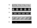
- FIG. 9 shows an optical micrograph when laser repair is performed at five locations under the above conditions.
- the deformation of the second electrode is confirmed, and in the dark-field photograph (FIG. 9B), the rectangular shape of the laser light irradiation region and the reflected light are in the center. It has been confirmed.
- the dark field image when the light is substantially perpendicular to the optical axis of the lens (parallel to the substrate), the reflected light looks dark without being seen, that is, the second electrode is greatly deformed at the rectangular shape portion and the central portion thereof, It can be seen that the other portions are substantially parallel to the substrate.
- the second electrode has a very beautiful repair mark as can be seen from FIG. 9B.
- the bright spot that can be seen at the center of the repair mark in FIG. 9B is the place where the deformed second electrode and the metal protective film are in contact with each other.
- the repair shape (repair space S) is maintained in addition to the physical properties unique to the metal. There is also an effect of joining by contact. Moreover, it can be seen from the photograph at the time of light emission from the substrate side (FIG. 9C) that the laser repair portion is insulated and no current flows and no light is emitted.
- the present invention it is possible to repair a short circuit by laser repair, and further, since the metal protective layer at that location is not destroyed, it is possible to prevent the deterioration factor of the organic electroluminescent element from entering the laser repair location. .
- SYMBOLS 100 Organic electroluminescent element 110 Substrate 120 Element main body 121 First electrode (anode) 122 Organic layer 123 Second electrode (cathode) DESCRIPTION OF SYMBOLS 130 Laser repair layer 131 Buffer layer 132 Metal protective layer 150 Light emission area
Landscapes
- Engineering & Computer Science (AREA)
- Manufacturing & Machinery (AREA)
- Electroluminescent Light Sources (AREA)
Abstract
La présente invention a pour objectif de proposer un élément électroluminescent organique à champ électrique avec lequel il est facile de rétablir un court-circuit par réparation laser. Pour ce faire, un élément électroluminescent organique à champ électrique comprend : une première électrode, qui est formée sur un substrat transparent ; une couche organique formée à partir d'une ou de plusieurs couches d'un matériau organique qui comprend une couche électroluminescente recouvrant la première électrode ; et une seconde électrode, qui recouvre la couche organique. Ledit élément électroluminescent comporte une partie dans laquelle le chevauchement de la première et de la seconde électrode est traité en tant que région électroluminescente. L'élément électroluminescent organique à champ électrique comprend également : une zone tampon, formée à partir d'un matériau organique qui recouvre la seconde électrode ; et une couche de protection métallique, formée à partir soit d'un métal soit d'un alliage, et qui recouvre la zone tampon. La couche de protection métallique est disposée au moins sur la région électroluminescente.
Priority Applications (1)
| Application Number | Priority Date | Filing Date | Title |
|---|---|---|---|
| PCT/JP2011/064121 WO2012176276A1 (fr) | 2011-06-21 | 2011-06-21 | Élément électroluminescent organique à champ électrique |
Applications Claiming Priority (1)
| Application Number | Priority Date | Filing Date | Title |
|---|---|---|---|
| PCT/JP2011/064121 WO2012176276A1 (fr) | 2011-06-21 | 2011-06-21 | Élément électroluminescent organique à champ électrique |
Publications (1)
| Publication Number | Publication Date |
|---|---|
| WO2012176276A1 true WO2012176276A1 (fr) | 2012-12-27 |
Family
ID=47422158
Family Applications (1)
| Application Number | Title | Priority Date | Filing Date |
|---|---|---|---|
| PCT/JP2011/064121 Ceased WO2012176276A1 (fr) | 2011-06-21 | 2011-06-21 | Élément électroluminescent organique à champ électrique |
Country Status (1)
| Country | Link |
|---|---|
| WO (1) | WO2012176276A1 (fr) |
Cited By (2)
| Publication number | Priority date | Publication date | Assignee | Title |
|---|---|---|---|---|
| CN112531132A (zh) * | 2019-12-18 | 2021-03-19 | 固安翌光科技有限公司 | 一种有机电致发光器件 |
| US11910696B2 (en) * | 2020-11-09 | 2024-02-20 | Jdi Design And Development G.K. | Self-luminous display panel and self-luminous display panel manufacturing method |
Citations (4)
| Publication number | Priority date | Publication date | Assignee | Title |
|---|---|---|---|---|
| JP3290375B2 (ja) * | 1997-05-12 | 2002-06-10 | 松下電器産業株式会社 | 有機電界発光素子 |
| JP2009009792A (ja) * | 2007-06-27 | 2009-01-15 | Kyocera Corp | 有機elディスプレイ及びその製造方法 |
| JP2009076437A (ja) * | 2007-08-31 | 2009-04-09 | Toshiba Matsushita Display Technology Co Ltd | 表示装置 |
| JP2009245734A (ja) * | 2008-03-31 | 2009-10-22 | Rohm Co Ltd | 有機el素子 |
-
2011
- 2011-06-21 WO PCT/JP2011/064121 patent/WO2012176276A1/fr not_active Ceased
Patent Citations (4)
| Publication number | Priority date | Publication date | Assignee | Title |
|---|---|---|---|---|
| JP3290375B2 (ja) * | 1997-05-12 | 2002-06-10 | 松下電器産業株式会社 | 有機電界発光素子 |
| JP2009009792A (ja) * | 2007-06-27 | 2009-01-15 | Kyocera Corp | 有機elディスプレイ及びその製造方法 |
| JP2009076437A (ja) * | 2007-08-31 | 2009-04-09 | Toshiba Matsushita Display Technology Co Ltd | 表示装置 |
| JP2009245734A (ja) * | 2008-03-31 | 2009-10-22 | Rohm Co Ltd | 有機el素子 |
Cited By (7)
| Publication number | Priority date | Publication date | Assignee | Title |
|---|---|---|---|---|
| CN112531132A (zh) * | 2019-12-18 | 2021-03-19 | 固安翌光科技有限公司 | 一种有机电致发光器件 |
| CN112531133A (zh) * | 2019-12-18 | 2021-03-19 | 固安翌光科技有限公司 | 一种有机电致发光器件 |
| CN112531133B (zh) * | 2019-12-18 | 2022-11-04 | 固安翌光科技有限公司 | 一种有机电致发光器件 |
| CN112531132B (zh) * | 2019-12-18 | 2023-07-04 | 固安翌光科技有限公司 | 一种有机电致发光器件 |
| EP4050674A4 (fr) * | 2019-12-18 | 2023-12-06 | Gu'an Yeolight Technology Co., Ltd. | Dispositif électroluminescent organique |
| US12185562B2 (en) | 2019-12-18 | 2024-12-31 | Gu' An Yeolight Technology Co., Ltd. | Organic electroluminescent device |
| US11910696B2 (en) * | 2020-11-09 | 2024-02-20 | Jdi Design And Development G.K. | Self-luminous display panel and self-luminous display panel manufacturing method |
Similar Documents
| Publication | Publication Date | Title |
|---|---|---|
| JP5757244B2 (ja) | 有機電界発光素子の製造方法、有機電界発光素子、表示装置及び照明装置 | |
| JP5694019B2 (ja) | 有機電界発光素子、表示装置および照明装置 | |
| KR102122188B1 (ko) | 유기 전계 발광 소자 및 유기 전계 발광 디바이스 | |
| JP5499482B2 (ja) | 有機電界発光素子、有機elディスプレイおよび有機el照明 | |
| JP5884213B2 (ja) | 有機電界発光素子の製造方法、有機電界発光素子、有機elディスプレイ及び有機el照明 | |
| JP2009266814A (ja) | 有機電界発光素子の製造方法、有機電界発光素子、有機elディスプレイ及び有機el照明 | |
| JP5757370B2 (ja) | 有機電界発光素子、有機el照明および有機el表示装置 | |
| JP5321700B2 (ja) | 有機電界発光素子、有機el照明および有機el表示装置 | |
| JP2010239125A (ja) | 有機電界発光素子、有機elディスプレイおよび有機el照明 | |
| WO2013150592A1 (fr) | Panneau électroluminescent organique et son procédé de fabrication | |
| JP2010199296A (ja) | 有機電界発光素子、有機elディスプレイおよび有機el照明 | |
| JP2010209320A (ja) | 有機電界発光素子用組成物、有機電界発光素子の製造方法、有機電界発光素子、有機elディスプレイ及び有機el照明 | |
| JP5423064B2 (ja) | 有機電界発光素子用組成物、有機電界発光素子、有機elディスプレイ及び有機el照明 | |
| WO2012176276A1 (fr) | Élément électroluminescent organique à champ électrique | |
| JP5402703B2 (ja) | 有機電界発光素子、有機elディスプレイ、有機el照明及び有機el信号装置 | |
| WO2012090560A1 (fr) | Élément électroluminescent organique et son procédé de fabrication | |
| WO2011019025A1 (fr) | Elément électroluminescent organique, dispositif daffichage électroluminescent organique, et dispositif déclairage électroluminescent organique | |
| WO2013035143A1 (fr) | Procédé de fabrication de panneau électroluminescent organique | |
| JP2010235708A (ja) | 蛍光発光材料、有機電界発光素子用組成物、有機電界発光素子、有機elディスプレイ及び有機el照明 | |
| JP5456282B2 (ja) | 有機電界発光素子 | |
| JP2010209143A (ja) | 有機電界発光素子用組成物、有機電界発光素子、有機elディスプレイおよび有機el照明 | |
| WO2013150593A1 (fr) | Panneau électroluminescent organique et son procédé de fabrication | |
| JP2010192474A (ja) | 有機電界発光素子、有機elディスプレイ及び有機el照明 | |
| JP2010238606A (ja) | 有機電界発光素子、有機elディスプレイ及び有機el照明。 | |
| JP2018117035A (ja) | 有機エレクトロルミネッセンス素子 |
Legal Events
| Date | Code | Title | Description |
|---|---|---|---|
| 121 | Ep: the epo has been informed by wipo that ep was designated in this application |
Ref document number: 11868344 Country of ref document: EP Kind code of ref document: A1 |
|
| NENP | Non-entry into the national phase |
Ref country code: DE |
|
| 122 | Ep: pct application non-entry in european phase |
Ref document number: 11868344 Country of ref document: EP Kind code of ref document: A1 |
|
| NENP | Non-entry into the national phase |
Ref country code: JP |