WO2012176338A1 - Dispositif de conversion d'énergie électrique, dispositif de commande de conversion d'énergie électrique, procédé de conversion d'énergie électrique, et programme - Google Patents
Dispositif de conversion d'énergie électrique, dispositif de commande de conversion d'énergie électrique, procédé de conversion d'énergie électrique, et programme Download PDFInfo
- Publication number
- WO2012176338A1 WO2012176338A1 PCT/JP2011/064589 JP2011064589W WO2012176338A1 WO 2012176338 A1 WO2012176338 A1 WO 2012176338A1 JP 2011064589 W JP2011064589 W JP 2011064589W WO 2012176338 A1 WO2012176338 A1 WO 2012176338A1
- Authority
- WO
- WIPO (PCT)
- Prior art keywords
- power
- supply
- supplied
- capacitor
- current source
- Prior art date
- Legal status (The legal status is an assumption and is not a legal conclusion. Google has not performed a legal analysis and makes no representation as to the accuracy of the status listed.)
- Ceased
Links
Images


Classifications
-
- H—ELECTRICITY
- H02—GENERATION; CONVERSION OR DISTRIBUTION OF ELECTRIC POWER
- H02M—APPARATUS FOR CONVERSION BETWEEN AC AND AC, BETWEEN AC AND DC, OR BETWEEN DC AND DC, AND FOR USE WITH MAINS OR SIMILAR POWER SUPPLY SYSTEMS; CONVERSION OF DC OR AC INPUT POWER INTO SURGE OUTPUT POWER; CONTROL OR REGULATION THEREOF
- H02M7/00—Conversion of AC power input into DC power output; Conversion of DC power input into AC power output
- H02M7/02—Conversion of AC power input into DC power output without possibility of reversal
- H02M7/04—Conversion of AC power input into DC power output without possibility of reversal by static converters
- H02M7/12—Conversion of AC power input into DC power output without possibility of reversal by static converters using discharge tubes with control electrode or semiconductor devices with control electrode
- H02M7/21—Conversion of AC power input into DC power output without possibility of reversal by static converters using discharge tubes with control electrode or semiconductor devices with control electrode using devices of a triode or transistor type requiring continuous application of a control signal
- H02M7/217—Conversion of AC power input into DC power output without possibility of reversal by static converters using discharge tubes with control electrode or semiconductor devices with control electrode using devices of a triode or transistor type requiring continuous application of a control signal using semiconductor devices only
-
- H—ELECTRICITY
- H02—GENERATION; CONVERSION OR DISTRIBUTION OF ELECTRIC POWER
- H02M—APPARATUS FOR CONVERSION BETWEEN AC AND AC, BETWEEN AC AND DC, OR BETWEEN DC AND DC, AND FOR USE WITH MAINS OR SIMILAR POWER SUPPLY SYSTEMS; CONVERSION OF DC OR AC INPUT POWER INTO SURGE OUTPUT POWER; CONTROL OR REGULATION THEREOF
- H02M1/00—Details of apparatus for conversion
- H02M1/0067—Converter structures employing plural converter units, other than for parallel operation of the units on a single load
- H02M1/007—Plural converter units in cascade
Definitions
- the present invention relates to a power conversion device, a power conversion control device, a power conversion method, and a program.
- Patent Document 1 discloses a device using a magnetic energy regenerative switch (MERS: Magnetic Energy Recovery Switch) having four reverse conducting switches and a capacitor.
- the power conversion device described in Patent Literature 1 includes two reverse conducting switches (one pair) located on one diagonal and two reverse conducting switches (the other pair) located on the other diagonal. Each of the reverse conduction switches is periodically turned on and off.
- the power conversion device described in Patent Literature 1 can change the polarity of the current depending on which of the above two pairs is switched on and off, thereby changing the power supply direction. In other words, the power conversion device described in Patent Document 1 changes the polarity of the current depending on whether one of the pair and the other pair is switched on or off, thereby supplying power. Can be changed.
- the present invention has been made in view of the above points, and an object of the present invention is to change the direction of power supply in power supply when a current source capable of supplying power is used.
- An object of the present invention is to provide a power conversion device, a power conversion control device, a power conversion method, and a program.
- a power conversion device includes: A first connection unit including an AC power source and a thyristor connected to the AC power source, and connected to a current source capable of being supplied with a first power; A second connection connected to a voltage source capable of being supplied with second power; A capacitor and a plurality of reverse conducting switches connected to the capacitor, and switching the on / off of the plurality of reverse conducting switches to generate magnetic energy generated in a predetermined inductor as electrostatic energy.
- a magnetic energy regenerative switch that performs any of the second supply to the current source;
- a control unit that controls the timing of turning on the thyristor to control the direction of current flow through the thyristor, and The control unit causes the magnetic energy regenerative switch to perform either the first supply or the second supply by changing a timing of turning on the thyristor. It is characterized by that.
- a power conversion device provides: A first connection connected to a current source capable of being supplied with a first power; A second connection connected to a voltage source capable of being supplied with second power; A capacitor, and a plurality of reverse conducting switches connected to the capacitor, wherein the magnetic energy generated in a predetermined inductor is changed to electrostatic energy by switching on and off of the plurality of reverse conducting switches.
- a first supply that converts power from the current source into the second power by supplying and discharging to the voltage source, and converts power from the voltage source into the first power to convert the power to the first power.
- a magnetic energy regenerative switch that performs any one of the second supply to the current source;
- a control unit that controls the switching of each of the plurality of reverse conduction switches to turn on and off, and causes the magnetic energy regeneration switch to perform the first supply and the second supply, and
- the control unit causes the magnetic energy regenerative switch to perform either the first supply or the second supply by changing a length of an ON period of each of the plurality of reverse conducting switches.
- a power conversion control device provides: A first connection unit including an AC power source and a thyristor connected to the AC power source, and connected to a current source capable of being supplied with a first power; A second connection connected to a voltage source capable of being supplied with second power; A capacitor and a plurality of reverse conducting switches connected to the capacitor, and switching the on / off of the plurality of reverse conducting switches to generate magnetic energy generated in a predetermined inductor as electrostatic energy.
- a first connection unit including an AC power source and a thyristor connected to the AC power source, and connected to a current source capable of being supplied with a first power
- a second connection connected to a voltage source capable of being supplied with second power
- a capacitor and a plurality of reverse conducting switches connected to the capacitor, and switching the on / off of the plurality of reverse conducting switches to generate magnetic energy generated in a predetermined inductor as electrostatic energy.
- a power conversion control device that controls a power conversion unit including a magnetic energy regenerative switch that performs any one of the second supply to be supplied to the current source, A control unit for controlling a flow direction of a current flowing through the thyristor by controlling timing of turning on the thyristor; The control unit causes the magnetic energy regenerative switch to perform either the first supply or the second supply by changing a timing of turning on the thyristor. It is characterized by that.
- a power conversion control device provides: A first connection connected to a current source capable of being supplied with a first power; A second connection connected to a voltage source capable of being supplied with second power; A capacitor, and a plurality of reverse conducting switches connected to the capacitor, wherein the magnetic energy generated in a predetermined inductor is changed to electrostatic energy by switching on and off of the plurality of reverse conducting switches.
- a power conversion control device that controls a power conversion unit including a magnetic energy regenerative switch that performs any one of a second supply to be supplied to a current source,
- a control unit that controls the switching of each of the plurality of reverse conduction switches to turn on and off, and causes the magnetic energy regeneration switch to perform the first supply and the second supply, and
- the control unit causes the magnetic energy regenerative switch to perform either the first supply or the second supply by changing a length of an ON period of each of the plurality of reverse conducting switches.
- a power conversion method includes: A first connection unit including an AC power source and a thyristor connected to the AC power source, and connected to a current source capable of being supplied with a first power; A second connection connected to a voltage source capable of being supplied with second power; A capacitor and a plurality of reverse conducting switches connected to the capacitor, and switching the on / off of the plurality of reverse conducting switches to generate magnetic energy generated in a predetermined inductor as electrostatic energy.
- the control step includes a step of causing the magnetic energy regenerative switch to perform either the first supply or the second supply by changing a timing at which the thyristor is turned on. It is characterized by that.
- a power conversion method includes: A first connection connected to a current source capable of being supplied with a first power; A second connection connected to a voltage source capable of being supplied with second power; A capacitor, and a plurality of reverse conducting switches connected to the capacitor, wherein the magnetic energy generated in a predetermined inductor is changed to electrostatic energy by switching on and off of the plurality of reverse conducting switches.
- a first supply that converts power from the current source into the second power by supplying and discharging to the voltage source, and converts power from the voltage source into the first power to convert the power to the first power.
- a power conversion method using a power conversion unit comprising: a magnetic energy regenerative switch that performs any one of a second supply to be supplied to a current source, A control step of causing the magnetic energy regenerative switch to perform the first supply and the second supply by controlling switching of each of the plurality of reverse conduction switches to ON and OFF; The control step causes the magnetic energy regeneration switch to perform either the first supply or the second supply by changing a length of an ON period of each of the plurality of reverse conducting switches. Including steps, It is characterized by that.
- a program according to the seventh aspect of the present invention provides: A first connection unit including an AC power source and a thyristor connected to the AC power source, and connected to a current source capable of being supplied with a first power; A second connection connected to a voltage source capable of being supplied with second power; A capacitor and a plurality of reverse conducting switches connected to the capacitor, and switching the on / off of the plurality of reverse conducting switches to generate magnetic energy generated in a predetermined inductor as electrostatic energy.
- a first connection unit including an AC power source and a thyristor connected to the AC power source, and connected to a current source capable of being supplied with a first power
- a second connection connected to a voltage source capable of being supplied with second power
- a capacitor and a plurality of reverse conducting switches connected to the capacitor, and switching the on / off of the plurality of reverse conducting switches to generate magnetic energy generated in a predetermined inductor as electrostatic energy.
- a computer that controls a power conversion unit including a magnetic energy regenerative switch that performs any one of the second supply to be supplied to the current source, Controlling the timing of turning on the thyristor to control the flow direction of the current flowing through the thyristor;
- the control step includes a step of causing the magnetic energy regenerative switch to perform either the first supply or the second supply by changing a timing at which the thyristor is turned on. It is characterized by that.
- a program according to the eighth aspect of the present invention provides: A first connection connected to a current source capable of being supplied with a first power; A second connection connected to a voltage source capable of being supplied with second power; A capacitor, and a plurality of reverse conducting switches connected to the capacitor, wherein the magnetic energy generated in a predetermined inductor is changed to electrostatic energy by switching on and off of the plurality of reverse conducting switches.
- a first supply that converts power from the current source into the second power by supplying and discharging to the voltage source, and converts power from the voltage source into the first power to convert the power to the first power.
- the direction of power supply can be changed in power supply when a current source capable of supplying power is used.
- FIG. 2 is a diagram illustrating a graph for explaining a power supply direction and the like in the circuit configuration of FIG. 1.
- FIG. 2 is a diagram illustrating a graph for explaining a power supply direction and the like in the circuit configuration of FIG. 1.
- FIG. 2 is a diagram illustrating a graph for explaining a power supply direction and the like when the length of an on period of a control signal is changed in the circuit configuration of FIG. 1.
- FIG. 2 shows the circuit structure of the power converter device which concerns on Embodiment 2 of this invention.
- FIG. 7 is a diagram illustrating a graph for explaining a power supply direction and the like when the delay phase angle of the control signal is changed in the circuit configuration of FIG. 6. It is a figure which shows the circuit structure of the power converter device which concerns on the modification of Embodiment 1 of this invention. It is a figure which shows the circuit structure of the power converter device which concerns on the modification of Embodiment 2 of this invention.
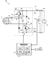
- the power conversion device 100 includes a first connection unit 101, a second connection unit 102, a capacitor C 1, an inductor L 1, a magnetic energy regenerative switch (hereinafter referred to as MERS) 105, an inductor L 2, and a control device 110. Is provided.
- the first connection unit 101 includes a pair of terminals connected to the outside, and is connected to the current source 11.
- the current source 11 can be supplied not only with power but also with power. That is, the current source 11 also functions as a load. In the current source 11, the polarity of the current does not change, but the polarity of the voltage can change depending on the supply direction of the power (that is, depending on whether power is supplied to or supplied to the current source 11).
- the current source 11 is a superconducting power storage device (SMES: Superconductive Magnetic Energy Storage).
- SMES Superconductive Magnetic Energy Storage
- the second connection unit 102 includes a pair of terminals connected to the outside and is connected to the voltage source 13.
- the voltage source 13 can be supplied not only with power but also with power. That is, the voltage source 13 also functions as a load. In the voltage source 13, the polarity of the voltage does not change depending on the supply direction of the power (that is, depending on whether power is supplied to or supplied to the voltage source 13), but the polarity of the current can change.
- the voltage source 13 is, for example, a DC bus connected to a generator of a power plant, a transformer of a substation, or the like. For example, power can be supplied to the DC bus for the purpose of selling power.
- the DC bus is a high voltage low current DC power supply that supplies low current power at a high voltage (for example, 50 kV or more).
- the power supplied by SMES is lower voltage and higher current than the power supplied by the DC bus.
- the capacitor C1 has both ends connected to the first connecting portion 101. That is, the capacitor C1 is connected in parallel with the current source 11 (first connection unit 101).
- the inductor L1 is composed of a choke coil or the like. One end of the inductor L1 is connected to the negative side of the first connection unit 101 (for example, the negative terminal connected to the negative side of the current source 11) and the capacitor C1, and the other end is connected to the MERS 105.
- the MERS 105 includes connection points N1 to N4, a reverse conduction switch SW1, a diode D2, a diode D3, a reverse conduction switch SW4, and a capacitor CM.
- connection point N1 The other end of the inductor L1 is connected to the connection point N1.
- the connection point N ⁇ b> 2 is connected to the negative electrode side of the first connection part 101.
- the connection point N3 is connected to the inductor L2.
- the connection point N4 is connected to the negative electrode side of the second connection unit 102 (for example, the negative electrode terminal connected to the negative electrode side of the voltage source 13).
- the reverse conducting switch SW1 includes a switch part (switching element part) S1 and a diode part (diode part) D1 connected in parallel.
- the reverse conducting switch SW1 is an IGBT (Insulated Gate Bipolar Transistor).
- the switch part S1 is a part of an IGBT self-extinguishing element
- the diode part D1 is a part of a parasitic diode of the IGBT.
- the switch unit S1 includes a gate (control terminal) G1.
- the gate G1 is supplied with either an on signal or an off signal, which is a control signal (gate signal), from the control device 110.
- the switch unit S1 is turned on when an ON signal among the control signals is supplied to the gate G1.
- the switch unit S1 is also turned on as the reverse conduction switch SW1 is turned on.
- the switch part S1 becomes conductive and short-circuits both ends of the diode part D1. That is, the reverse conduction type switch SW1 becomes conductive when it is turned on when the ON signal is supplied.
- the switch unit S1 is turned off when an off signal of the control signal is supplied to the gate G1. Switching off the switch unit S1 is also turning off the reverse conducting switch SW1.
- the switch unit S1 When the switch unit S1 is turned off, the switch unit S1 is turned off. That is, the reverse conduction type switch SW1 functions as the diode part D1 when the OFF signal is supplied and turned off. That is, the reverse conducting switch SW1 becomes conductive when turned on, and functions as a diode when turned off.
- the reverse conducting switch SW1 is connected between the connection point N1 and the connection point N3 in such a direction that the anode of the diode part D1 is connected to the connection point N1 and the cathode is connected to the connection point N3.
- the reverse conduction type switch SW4 has the same configuration as the reverse conduction type switch SW1.
- the switch unit S4 corresponds to the switch unit S1
- the gate G4 corresponds to the gate G1
- the diode unit D4 corresponds to the diode unit D1.
- the reverse conduction switch SW4 becomes conductive when turned on by the supply of the on signal among the control signals, and turns off by the supply of the off signal of the control signals. It functions as a diode part D4 (diode).
- the reverse conducting switch SW4 is connected between the connection point N2 and the connection point N4 in such a direction that the anode of the diode part D4 is connected to the connection point N4 and the cathode is connected to the connection point N2.
- the diode D2 and the diode D3 are each composed of a single element independent of the reverse conducting switch.
- the diode D2 has an anode connected to the connection point N4 and a cathode connected to the N1.
- the diode D3 has an anode connected to the node N2 and a cathode connected to the connection point N3.
- the capacitor CM has both ends connected to the connection point N3 and the connection point N4.
- the capacitor CM stores and discharges the magnetic energy generated in the inductor L1 as electrostatic energy in accordance with the on / off switching of the reverse conducting switch SW1 and the reverse conducting switch SW4. That is, the capacitor CM is used to regenerate the magnetic energy as electrostatic energy.
- the inductor L2 is composed of a choke coil or the like. One end of the inductor L1 is connected to the MERS 105 (connection point N3), and the other end is connected to the positive side of the second connection unit 102 (for example, the positive terminal connected to the positive side of the voltage source 13).
- the control device 110 controls the MERS 105.
- the control device 110 is configured by a predetermined circuit or the like that can perform processing described later.
- the control device 110 includes a CPU (Central Processing Unit) 111, a RAM (Random Access Memory) 112, a ROM (Read Only Memory) 113, and an input / output unit 114.
- a CPU Central Processing Unit
- RAM Random Access Memory
- ROM Read Only Memory
- the CPU 111 executes the following processing performed by the control device 110 in accordance with a program stored in the ROM 113.
- the RAM 112 functions as a main memory for the CPU 111.
- the ROM 113 stores programs and various data used by the CPU 111 during the following processing.
- the CPU 111 performs the following processing using data stored in the ROM 113 as appropriate.
- the input / output unit 114 includes various ports and is connected to the reverse conduction switches SW1 and SW4 of the MERS 105 and the like. Control signals and the like input / output to / from the control device 110 are input / output to / from the CPU 111 via the input / output unit 114.
- the ROM 113, RAM 112, etc. can be changed to other storage devices (flash memory, etc.) as appropriate.
- the control device 110 controls the MERS 105 by supplying a control signal to each of the gates G1 and G4 and switching each of the reverse conducting switches SW1 and SW4 on and off.
- the circuit of FIG. 1 can take the following circuit conditions, for example.
- Capacitance of capacitor CM 4 ⁇ F
- Inductance of inductor L1 1 mH
- Capacitance of capacitor C1 100 ⁇ F
- Inductance of current source 11 100H
- initial current value of current source 11 10A
- Inductor L2 10 mH
- Output voltage of the voltage source 500 kV
- the control device 110 supplies the reverse conduction type switches SW1 and SW4 with a control signal in which the ON signal and the OFF signal are repeated.
- the control device 110 supplies the same control signal to the reverse conduction switches SW1 and SW4, thereby switching on / off of the reverse conduction switch SW1 and on / off of the reverse conduction switch SW4 in synchronization.
- the frequency of the control signal (frequency at the time of switching the on signal) is 2000 Hz
- the period of each on signal of the control signal is 115 ⁇ sec.
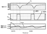
- FIG. 2 shows the voltage value Vc of the capacitor CM, the voltage value Vg of the control signal, the current value Idc of the inductor L2, and the voltage value Vcurr of the capacitor C1 in the circuit operation under the above circuit conditions (including the control signal conditions). Show.
- the control signal when the control signal is turned off, that is, when the reverse conducting switches SW1 and SW4 are turned off, the voltage value Vc of the capacitor CM is increased, so that the capacitor CM is charged. I understand. Further, when the control signal is turned on, that is, when the reverse conducting switches SW1 and SW4 are turned on, the voltage value Vc of the capacitor CM is decreased, and it can be seen that the capacitor CM is discharged. Thus, the capacitor CM is charged / discharged in accordance with the switching of the reverse conduction switches SW1 and SW4 between on and off. At this time, the magnetic energy generated in the inductor L1 is stored (charged) and discharged (discharged) in the capacitor CM as electrostatic energy (charge). That is, the magnetic energy generated in the inductor L1 is regenerated by charging and discharging the capacitor CM of the magnetic energy regenerative switch 105.
- the current value Idc of the inductor L2 varies periodically according to switching of the reverse conduction switches SW1 and SW4 between on and off, but the average value is ⁇ 0.77 kA. Since the current value Idc of the inductor L2 has a negative value in the direction in which the current flows from the positive electrode of the voltage source 13, the current flows from the voltage source 13 to the current source 11. According to the simulation results, the current source 11 is charged with an average power of 365 MW per second.
- the voltage value Vcurr of the capacitor C1 is substantially constant but takes a negative value. Since the voltage value Vcurr is set to take a positive value when the current source 11 supplies power, this also shows that the current source 11 is charged.
- the current value Idc of the inductor L2 varies periodically according to the switching of the reverse conducting switches SW1 and SW4 between on and off, but the average value is +0.7 kA. Therefore, contrary to the case of FIG. 2, the current in this case flows from the current source 11 to the voltage source 13. According to the simulation results, the current source 11 is charged with an average power of 385 MW per hour.
- the voltage value Vcurr of the capacitor C1 is substantially constant but takes a positive value. Since the voltage value Vcurr is set to take a positive value when the current source 11 supplies power, it can be seen from this that power is supplied to the current source 11.
- FIG. 2 is a diagram illustrating the relationship between the current value I (SW1) flowing through the reverse conducting switch SW1, the voltage value V (SW1) applied to the reverse conducting switch SW1, and the voltage value Vg of the control signal in the circuit operation of FIG. 4 shows.
- the current flowing through the reverse conducting switch SW4 and the applied voltage are the same as those of the reverse conducting switch SW1.
- the current value I (SW1) is 0 at the timing when the control signal switches from the off signal to the on signal. That is, no current flows through the reverse conduction switch SW1 at the timing when the reverse conduction switch SW1 is turned on.
- the voltage value V (SW1) is 0 at the timing when the control signal switches from the on signal to the off signal. That is, as can be seen with reference to FIG. 2 and FIG. 3, the discharge of the capacitor CM is completed during the ON signal period of the control signal, and the reverse conduction switch SW1 is turned on at the timing when the reverse conduction switch SW1 is turned off. No voltage is applied.
- soft switching is realized in the MERS 105. And such soft switching implement
- the discharge period and the charge period depend on the relationship between the capacitance of the capacitor CM and the inductance of the inductor L1, the control signal ON signal, the OFF signal period, the capacitor CM, and the like so that the above soft switching is realized. And the inductance of the inductor L1 may be determined. Further, the capacitance of the capacitor CM and the inductance of the inductor L1 may be determined so that the capacitor CM is charged and discharged at a moderate speed as described above.
- the inductor L2 has a sufficiently larger inductance than the inductor L1 under the above-described conditions (conditions in FIGS. 2 to 4). Thereby, the charging / discharging of the capacitor CM is dominated by resonance with the inductor L1. Therefore, the inductor L2 can behave like a current source together with the voltage source 13 connected in series with the inductor L2.
- the inductor L2 may have a larger inductance than the inductor L1 so that such behavior can be achieved.
- the capacitor C1 and the inductor L1 constitute a smoothing filter that smoothes the current flowing into the current source 11.
- the capacitor C1 has a sufficiently larger capacitance than the capacitor CM, it is possible to prevent a high voltage from being applied to the current source 11 when the current source 11 is charged.
- the current source 11 is SMES and includes a superconducting coil, but the superconducting coil has a low withstand voltage (that is, it can be said that the withstand voltage of the current source 11 is low).
- the capacitance of the capacitor C1 is large, it is prevented that a high voltage (that is, a voltage higher than the withstand voltage is applied) is applied to the current source 11 when the current source 11 is charged. Thus, the superconducting coil can be protected.
- the capacitance of the capacitor C1 is preferably set to a value larger than the capacitance of the capacitor CM that prevents the voltage higher than the withstand voltage from being applied to the current source 11.
- the current Icoil flowing through the current source 11 (SMES superconducting coil), the voltage value Vc of the capacitor CM, and the voltage of the current source 11 (SMES superconducting coil) when the length of the ON period of the control signal is changed.
- the circuit conditions are the same as in FIG. In FIG.
- the control device 110 supplies the reverse conduction switch SW1 with an off signal control signal until 0.1 ⁇ s, thereby turning off the reverse conduction switch SW1 while turning on the reverse conduction switch SW4.
- the reverse conduction switch SW4 is kept on by supplying the control signal.
- the control device 110 supplies the same control signal (a signal for alternately switching on and off signals) to the reverse conducting switches SW1 and SW4 after 0.01 seconds. From 0.01 second to 0.05 second, the ON period, which is the ON signal period of the control signal, is 115 ⁇ s, and after that (after 0.05 second), it is switched to 105 ⁇ s.
- the power supply direction is reversed due to the change in the length of the ON period of the control signal.
- the power value Wsmes and the power value Whvdc have substantially the same value (waveform) because they are in a power receiving relationship.
- the current value Icoil since the current source 11 is charged from 0.01 seconds to 0.05 seconds, the current value Icoil increases, and thereafter, current flows out from the current source 11. The current value Icoil is decreasing.
- the direction of power supply can be changed by changing the length of the ON period of the control signal. This is effective when the voltage source 13 is a voltage source having a higher voltage than the current source 11 (which means that the peak or average voltage is higher).
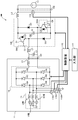
- the current source 11 of the first embodiment is configured to include an AC power supply 15, a thyristor converter (a portion formed by a plurality of thyristors) 16, and an inductor L3 (see FIG. 6).
- the AC power supply 15 is a power supply to which power can be supplied.
- parts different from the first embodiment will be mainly described, and description of the same parts as those of the first embodiment will be omitted as appropriate.
- FIG. 6 those corresponding to those of the first embodiment are denoted by the same reference numerals (the same applies to FIGS. 8 and 9).
- the AC power supply 15 constitutes a three-phase AC power supply and outputs a U-phase AC voltage, a V-phase AC voltage, and a W-phase AC voltage.
- the AC power supply 15 includes three AC power supplies and three inductors connected in series to the three AC power supplies in an equivalent circuit form.
- the thyristor converter 16 is connected to the AC power supply 15 and includes a plurality of thyristors according to the AC voltage output from the AC power supply 15.
- the thyristor converter 16 includes thyristors 16A to 16F arranged corresponding to the positive and negative of each of the three-phase alternating currents (U phase, V phase, W phase).
- the current source 11 also includes an inductor L3.
- the inductor L3 is connected between the thyristor converter 16 and the negative electrode side of the first connection unit 101.
- the inductor L3 has a sufficiently larger inductance than the inductor L1, and behaves as the current source 11 together with the AC power supply 15 and the thyristor converter 16. That is, the inductor L 3, the AC power supply 15, and the thyristor converter 16 are components of the current source 11.
- the control device 110 controls the on / off switching of the reverse conducting switches SW1 and SW4 of the MERS 105, as in the first embodiment. Further, the control device 110 also controls the thyristor converter 16. Specifically, control device 110 turns on thyristor 16A during a positive period of U-phase AC voltage and turns on thyristor 16B during a negative period of U-phase AC voltage. The control device 110 turns on the thyristor 16C during the positive period of the V-phase AC voltage and turns on the thyristor 16D during the negative period of the V-phase AC voltage.
- control device 110 turns on thyristor 16E during the positive period of the W-phase AC voltage, and turns on thyristor 16F during the negative period of the W-phase AC voltage.
- the control device 110 turns on each of the thyristors 16A to 16F by supplying an ON signal that is a control signal to each of the thyristors 16A to 16F, but immediately thereafter supplies an OFF signal that is a control signal. That is, the ON signal is a single pulse signal.
- the control device 110 sets the timing of turning on (ON signal supply timing) as a timing delayed by a predetermined phase angle from the time of zero crossing of each AC voltage (hereinafter referred to as a delayed phase angle).
- the control device 110 can change the lagging phase angle according to the power supply direction. Each thyristor continues to be turned on even when an off signal is supplied, and is turned off at the time of the zero crossing of each AC voltage (at the time of the first zero crossing after turning on).
- the circuit of FIG. 6 can take the following circuit conditions, for example.
- Capacitance of capacitor CM 4 ⁇ F
- Inductance of inductor L1 1 mH
- Capacitance of capacitor C1 100 ⁇ F
- Output voltage frequency of AC power supply 15 50 Hz
- Output voltage of AC power supply 15 66 kV
- Inductor L2 20 mH
- Output voltage of voltage source 13 500 kV
- Inductor L3 500 mH
- Inductance of each inductor of AC power supply 15 1.5 mH
- the control device 110 supplies the reverse conduction type switches SW1 and SW4 with a control signal in which the ON signal and the OFF signal are repeated.
- the control device 110 supplies the same control signal to the reverse conduction switches SW1 and SW4, thereby switching on / off of the reverse conduction switch SW1 and on / off of the reverse conduction switch SW4 in synchronization.
- the frequency of the control signal (frequency at which the on signal is switched) is 2000 Hz, and the period of each on signal of the control signal is 120 ⁇ sec.
- the control device 110 controls the lag phase angle of each control signal supplied to the thyristors 16A to 16F of the thyristor converter 16 (this is the lag phase angle for the ON signal, which can also be referred to as the ON signal supply timing). For example, the control device 110 switches the delay phase angle from 120 ° to 60 °. The delayed phase angle is the same for each control signal. For example, when the lag phase angle for each control signal is 60 °, the control signal supplied to the thyristor 16A is 60 ° from the zero crossing time when the U-phase AC voltage is switched from the negative period to the positive period.
- the control signal that is switched to the ON signal and supplied to the thyristor 16B the control signal that is switched to the ON signal at 60 ° from the zero crossing time when the positive phase in the U-phase AC voltage is switched to the negative period is supplied to the thyristor 16E. Then, the ON signal is switched at 60 ° from the zero crossing time when the AC phase voltage of the W phase is switched from the positive period to the negative period.
- W the current Idcin flowing through the inductor L3, the voltage value Vc of the capacitor C1, the voltage value Vload of the voltage source 13, and the voltage value Vdcin inputted to and outputted from the current source 11 (in the case of a negative value, the current
- the power is supplied to the source 11 and when the value is positive, the power is supplied to the voltage source 13.
- the power value W1 supplied by the current source 11 (when the value is negative, the current source is charged).
- the power value W2 supplied to the voltage source 13 (in the case of a negative value, it indicates that the voltage source 13 supplies power), and the thyristor converter 16
- the lag phase angle of each control signal supplied to each thyristor (each lag phase angle A is common.) And, shown in Figure 7.
- the control device 110 switches the delay phase angle from 120 ° to 60 ° at the timing after 0.15 seconds.
- the current value Idcin flowing through the inductor L3 is a combination of the three-phase AC current values I (U), I (V), and I (W), and is substantially constant.
- the voltage value Vload of the voltage source 13 is also constant.
- the lag phase angle is switched from 120 ° to 60 ° at the timing of 0.15 seconds, the polarity of the voltage value Vdcin, the power value W1, and the power value W2 is reversed, so the power supply direction changes.
- the delay phase angle is 120 °
- power is supplied from the voltage source 13 to the current source 11, and the current source 11 (AC power supply 15) is charged.
- the delayed phase angle is 60 °
- power is supplied from the current source 11 to the voltage source 13.
- the power The supply direction can be changed.
- soft switching or the like in the MERS 105 is also realized.
- the effect demonstrated in Embodiment 1 is suitably acquired also in this embodiment.
- the AC power supply 15 may be another power supply such as a single-phase AC power supply.
- the power supply direction is changed by changing the delay phase angle of the control signal. I can do it.
- the connection structure of the thyristor of the thyristor converter 16, the number of thyristors, and the like may be appropriately changed in accordance with the AC power supply.
- the various reverse conduction type switches described above may be composed of a plurality of elements in which a diode (diode part) and a switching element (switch part) are combined in parallel, or an N-channel silicon MOSFET (Metal-Oxide-).
- a reverse conducting semiconductor switch other than an IGBT having a switch portion and a diode portion such as a Semiconductor Field-Effect Transistor.
- the N-channel type silicon MOSFET generally has a lower withstand voltage than the IGBT.
- the diode D2 or D3 may be a diode portion of a reverse conducting switch.
- the control device 110 supplies a control signal of an off signal to the reverse conducting switch so that the reverse conducting switch functions as the diode D2 or D3.
- the control device 110 supplies a control signal of an ON signal to the reverse conducting switch only during the period when the current flows through the diode D2 or D3 when the MERS 105 is operated, so that the reverse conducting switch is turned on. Good. In such a case, the number of paths through which current flows increases, and current loss decreases.
- the current source 11 may be another current source, may not be a constant current source, and may not be a low voltage.
- the voltage source 13 may be another voltage source, may not be a constant voltage source, and may not be a high voltage. However, in this case, it is desirable to perform feedback control described later.
- control device 110 may be configured by a dedicated electronic circuit (ASIC (Application Specific Integrated) Circuit) or the like) that does not require a program.
- ASIC Application Specific Integrated
- the control device 110 determines the length of the ON period (first embodiment) of the control signal supplied to the MERS 105 or the delay phase angle of the thyristor converter 16 (second embodiment). By controlling, it is possible to adjust the supply and demand balance between the amount of power supplied from the voltage source 13 to the current source 11 and the amount of power supplied from the current source 11 to the voltage source 13. Since the power supply direction can be changed by this, the control device 110 controls the length of the ON period or the delay phase angle so as to maintain the voltage generated by the voltage source 13. May be. For example, as illustrated in FIGS. 8 and 9, a voltage detection unit 119 including a voltmeter or the like in the power conversion apparatus 100 is connected to the second connection unit 102 in parallel with the voltage source 13.
- the control device 110 acquires the voltage value detected by the power detection unit 119 (the voltage value of the voltage generated by the voltage source 13 and supplied to the control device 110 in the form of an electrical signal, for example). Then, the acquired voltage value is compared with a predetermined threshold value set in advance. For example, if the voltage value is equal to or greater than a predetermined threshold, the control unit controls the length of the on period or the delay phase angle to control the power supply direction to charge the current source 11. Further, for example, if the voltage value is less than a predetermined threshold, the control unit controls the length of the on period or the delay phase angle to charge the voltage source 11 (increase the output voltage). To control the supply direction. That is, the power supply direction is the direction from the current source 11 to the voltage source 13.
- the control device 110 sets the ON period to 105 ⁇ s, and in the case of FIG. 6 and the like, the control device 110 sets the delay phase angle to 60 °.
- the power supply direction is defined by controlling the ON period or the delay phase angle in accordance with the voltage generated by the voltage source 13, the stable operation of the voltage source 13 (the voltage source 13 is generated). It is effective to keep the voltage value of the voltage to be kept below a predetermined reference value). This is particularly effective when the voltage source 13 is composed of a high-voltage low-current DC power source as in the first and second embodiments.
- the predetermined threshold value is set in the control device 110 when the control device 110 stores it in advance in a storage device such as the ROM 113, for example.
- the control device 110 acquires the voltage value or current value at a predetermined position in the circuit, and based on the acquired voltage value or current value, the length of the ON period of the control signal supplied to the MERS 105 or thyristor conversion The delay phase angle of the control signal supplied to the device 16 may be changed. That is, the control device 110 may perform feedback control.
- voltage detectors 118 ⁇ / b> U, 118 ⁇ / b> V, 118 ⁇ / b> W for detecting the voltage of each phase of the three-phase alternating current are arranged in the power conversion device 100 and connected to the three-phase alternating current power supply 15. And the control apparatus 110 acquires the voltage value (It is the voltage value of the voltage of each phase, for example, is supplied to the control apparatus 110 in the form of an electric signal.) Which the voltage detection parts 118U, 118V, and 118W detected.
- the positive / negative of the voltage of each phase and the zero crossing time of the voltage of each phase are specified, and the timing corresponding to the lag phase angle is turned on based on the specified values (thyristors 16A to 16F are turned on, respectively) (Timing) is specified, and an ON signal is supplied to the corresponding thyristors 16A to 16F at the specified timing to turn it ON.
- control device 110 may perform switching of the power supply direction based on a user operation.
- an input unit 117 for example, a switch, an operation button, or the like
- the input unit performs an operation (switching of the switch,
- an operation signal indicating the accepted operation is supplied to the control device 110.
- the control device 110 is configured so that the supply direction specified by this operation is the actual power supply direction, or the length of the ON period of the control signal supplied to the MERS 105, or The lag phase angle of the control signal supplied to the thyristor converter 16 is changed.
- the control device 110 sets the on period to 115 ⁇ s, and in the case of FIG. 6 or the like, the control device 110 sets the delay phase angle. Set to 120 °.
Landscapes
- Engineering & Computer Science (AREA)
- Power Engineering (AREA)
- Inverter Devices (AREA)
Abstract
La présente invention concerne un dispositif de conversion d'énergie électrique (100) qui comprend les éléments suivants : une première section de connexion (101) qui est connectée à une source de courant (11) ; une deuxième section de connexion (102) qui est connectée à une source de tension (13) ; et un commutateur à récupération d'énergie magnétique (105) qui exécute soit une première alimentation dans laquelle l'énergie électrique en provenance de la source de courant (11) est convertie puis délivrée à la source de tension (13), soit une deuxième alimentation dans laquelle l'énergie électrique en provenance de la source de tension (13) est convertie et délivrée à la source de courant (11). Le dispositif de conversion d'énergie électrique (100) est en outre muni d'une unité de commande (110). L'unité de commande (110), en modifiant le synchronisme avec lequel les thyristors (16A-16F) de la source de courant (11) sont rendus passants, commande le commutateur à récupération d'énergie magnétique (105) pour qu'il exécute soit la première alimentation, soit la deuxième alimentation.
Priority Applications (1)
| Application Number | Priority Date | Filing Date | Title |
|---|---|---|---|
| PCT/JP2011/064589 WO2012176338A1 (fr) | 2011-06-24 | 2011-06-24 | Dispositif de conversion d'énergie électrique, dispositif de commande de conversion d'énergie électrique, procédé de conversion d'énergie électrique, et programme |
Applications Claiming Priority (1)
| Application Number | Priority Date | Filing Date | Title |
|---|---|---|---|
| PCT/JP2011/064589 WO2012176338A1 (fr) | 2011-06-24 | 2011-06-24 | Dispositif de conversion d'énergie électrique, dispositif de commande de conversion d'énergie électrique, procédé de conversion d'énergie électrique, et programme |
Publications (1)
| Publication Number | Publication Date |
|---|---|
| WO2012176338A1 true WO2012176338A1 (fr) | 2012-12-27 |
Family
ID=47422209
Family Applications (1)
| Application Number | Title | Priority Date | Filing Date |
|---|---|---|---|
| PCT/JP2011/064589 Ceased WO2012176338A1 (fr) | 2011-06-24 | 2011-06-24 | Dispositif de conversion d'énergie électrique, dispositif de commande de conversion d'énergie électrique, procédé de conversion d'énergie électrique, et programme |
Country Status (1)
| Country | Link |
|---|---|
| WO (1) | WO2012176338A1 (fr) |
Citations (6)
| Publication number | Priority date | Publication date | Assignee | Title |
|---|---|---|---|---|
| JPS61262038A (ja) * | 1985-05-15 | 1986-11-20 | 三菱電機株式会社 | 超電導コイル・エネルギ−貯蔵回路 |
| JPS63174566A (ja) * | 1987-01-09 | 1988-07-19 | Toshiba Corp | 電流形pwm変換装置 |
| JPH06327171A (ja) * | 1993-05-10 | 1994-11-25 | Toyota Motor Corp | 電力貯蔵装置 |
| JP2005223867A (ja) * | 2004-02-03 | 2005-08-18 | Ryuichi Shimada | 磁気エネルギー回生スイッチを用いた昇圧パルス電源装置 |
| JP2008035620A (ja) * | 2006-07-28 | 2008-02-14 | Fujitsu Access Ltd | 双方向dc−dcコンバータ |
| WO2009075366A1 (fr) * | 2007-12-11 | 2009-06-18 | Tokyo Institute Of Technology | Appareil de conversion de puissance à commutation douce |
-
2011
- 2011-06-24 WO PCT/JP2011/064589 patent/WO2012176338A1/fr not_active Ceased
Patent Citations (6)
| Publication number | Priority date | Publication date | Assignee | Title |
|---|---|---|---|---|
| JPS61262038A (ja) * | 1985-05-15 | 1986-11-20 | 三菱電機株式会社 | 超電導コイル・エネルギ−貯蔵回路 |
| JPS63174566A (ja) * | 1987-01-09 | 1988-07-19 | Toshiba Corp | 電流形pwm変換装置 |
| JPH06327171A (ja) * | 1993-05-10 | 1994-11-25 | Toyota Motor Corp | 電力貯蔵装置 |
| JP2005223867A (ja) * | 2004-02-03 | 2005-08-18 | Ryuichi Shimada | 磁気エネルギー回生スイッチを用いた昇圧パルス電源装置 |
| JP2008035620A (ja) * | 2006-07-28 | 2008-02-14 | Fujitsu Access Ltd | 双方向dc−dcコンバータ |
| WO2009075366A1 (fr) * | 2007-12-11 | 2009-06-18 | Tokyo Institute Of Technology | Appareil de conversion de puissance à commutation douce |
Non-Patent Citations (1)
| Title |
|---|
| ISOBE T ET AL.: "A soft-switching boost DC to AC converter without smoothing capacitor using a MERS pulse link concept", POWER ELECTRONICS CONFERENCE (IPEC), 2010 INTERNATIONAL, 21 June 2010 (2010-06-21), pages 2815 - 2821 * |
Similar Documents
| Publication | Publication Date | Title |
|---|---|---|
| EP3657661B1 (fr) | Circuit de conversion, procédé de commande, et dispositif d'alimentation électrique | |
| CN108258899B (zh) | 一种升压功率变换电路 | |
| CN100590958C (zh) | 带有分布储能器的多相变流器的控制方法 | |
| JP6951222B2 (ja) | 電力変換装置及び電力変換システム | |
| CN109075721B (zh) | 用于多电平转换器的模块 | |
| CN111181396A (zh) | 一种悬浮电容型多电平桥式电路及其控制方法 | |
| US10432101B2 (en) | Power conversion apparatus | |
| US20110019453A1 (en) | Electric circuit for converting direct current into alternating current | |
| US5642273A (en) | Resonant snubber inverter | |
| EP2966771B1 (fr) | Onduleur monophasé | |
| US10270328B2 (en) | Multilevel converter with energy storage | |
| US10003257B2 (en) | Converter | |
| US12040713B2 (en) | DC-DC converter of power conversion system | |
| WO2011052364A1 (fr) | Dispositif de conversion de puissance | |
| EP3726722A1 (fr) | Convertisseur de puissance entrelacé | |
| JP4358277B2 (ja) | Dc/dc電力変換装置 | |
| JP7099199B2 (ja) | 駆動対象スイッチの駆動回路 | |
| WO2022176589A1 (fr) | Convertisseur c.a.-c.c. | |
| KR101030776B1 (ko) | 승압형 직류/직류 변환기 | |
| EP3346594A1 (fr) | Circuit d'interruption périodique bidirectionnel | |
| Hosseinzadeh et al. | Back-to-back stacked multicell converter | |
| JP7835078B2 (ja) | 電力変換装置 | |
| WO2012176338A1 (fr) | Dispositif de conversion d'énergie électrique, dispositif de commande de conversion d'énergie électrique, procédé de conversion d'énergie électrique, et programme | |
| JP6444204B2 (ja) | 電力変換装置 | |
| CN118591975A (zh) | 电力转换系统的dc-dc转换器 |
Legal Events
| Date | Code | Title | Description |
|---|---|---|---|
| 121 | Ep: the epo has been informed by wipo that ep was designated in this application |
Ref document number: 11868152 Country of ref document: EP Kind code of ref document: A1 |
|
| NENP | Non-entry into the national phase |
Ref country code: DE |
|
| 122 | Ep: pct application non-entry in european phase |
Ref document number: 11868152 Country of ref document: EP Kind code of ref document: A1 |
|
| NENP | Non-entry into the national phase |
Ref country code: JP |