WO2012177101A2 - Duty cycle correction apparatus - Google Patents
Duty cycle correction apparatus Download PDFInfo
- Publication number
- WO2012177101A2 WO2012177101A2 PCT/KR2012/004999 KR2012004999W WO2012177101A2 WO 2012177101 A2 WO2012177101 A2 WO 2012177101A2 KR 2012004999 W KR2012004999 W KR 2012004999W WO 2012177101 A2 WO2012177101 A2 WO 2012177101A2
- Authority
- WO
- WIPO (PCT)
- Prior art keywords
- unit
- output
- averaging
- duty cycle
- cycle correction
- Prior art date
- Legal status (The legal status is an assumption and is not a legal conclusion. Google has not performed a legal analysis and makes no representation as to the accuracy of the status listed.)
- Ceased
Links
Images



Classifications
-
- H—ELECTRICITY
- H03—ELECTRONIC CIRCUITRY
- H03K—PULSE TECHNIQUE
- H03K3/00—Circuits for generating electric pulses; Monostable, bistable or multistable circuits
- H03K3/01—Details
- H03K3/017—Adjustment of width or dutycycle of pulses
-
- H—ELECTRICITY
- H03—ELECTRONIC CIRCUITRY
- H03K—PULSE TECHNIQUE
- H03K5/00—Manipulating of pulses not covered by one of the other main groups of this subclass
- H03K5/156—Arrangements in which a continuous pulse train is transformed into a train having a desired pattern
-
- H—ELECTRICITY
- H03—ELECTRONIC CIRCUITRY
- H03K—PULSE TECHNIQUE
- H03K5/00—Manipulating of pulses not covered by one of the other main groups of this subclass
- H03K5/156—Arrangements in which a continuous pulse train is transformed into a train having a desired pattern
- H03K5/1565—Arrangements in which a continuous pulse train is transformed into a train having a desired pattern the output pulses having a constant duty cycle
-
- H—ELECTRICITY
- H03—ELECTRONIC CIRCUITRY
- H03L—AUTOMATIC CONTROL, STARTING, SYNCHRONISATION OR STABILISATION OF GENERATORS OF ELECTRONIC OSCILLATIONS OR PULSES
- H03L7/00—Automatic control of frequency or phase; Synchronisation
- H03L7/06—Automatic control of frequency or phase; Synchronisation using a reference signal applied to a frequency- or phase-locked loop
- H03L7/08—Details of the phase-locked loop
- H03L7/081—Details of the phase-locked loop provided with an additional controlled phase shifter
Definitions
- the present invention relates to a duty cycle correction device.
- the duty cycle compensator is one of the circuits most widely used in a correction circuit of a digital system, a switching regulator used in a power supply circuit, or a delayed synchronous loop of a signal synchronization system. By correcting the cycle, it serves to reduce the error rate so that accurate data is transmitted.
- the change in the duty ratio caused by the path delay and the reflection path is corrected to 50%, so that the sampling signal of the system can accurately detect the data.
- the switch's exact duty ratio is adjusted to improve performance.
- the reception sensitivity is improved by accurately adjusting and synchronizing the duty ratio of the received signal data.
- a conventional duty cycle corrector necessarily requires a pulse generator, a complicated circuit is required to maintain an accurate pulse width, and a range in which the duty cycle can be corrected is limited.
- the retarder used in the conventional duty cycle corrector has its own delay error, and this error has a problem of making the duty ratio more inaccurate.
- the technical problem to be solved by the present invention is to provide a duty cycle correction device that minimizes its own error by not using a pulse generator and a delay.
- Another technical problem to be solved by the present invention is to provide a duty cycle correction device designed to be insensitive to process changes and temperature changes, thereby minimizing system performance degradation due to variation in the duty ratio of the input signal.
- the duty cycle correction apparatus of the present invention for correcting the duty ratio of the input signal, the adjustment unit for adjusting the signal width of the input signal; A first averaging unit for averaging the widths of the output signals of the adjusting unit; An inverter unit for inverting an output signal of the adjustment unit; A second averaging unit for averaging the widths of the output signals of the inverter unit; And a comparing unit comparing the output signals of the first and second averaging units and outputting the difference.
- the adjustment unit may adjust the width of the input signal using the output of the comparison unit.
- it may further include a selection unit for selecting the ratio of the output signal of the first averaged unit and the second averaged unit, so that the comparison unit outputs the difference according to the ratio.
- it may further include a first buffer unit for temporarily storing the output of the adjustment unit to output to the first averaging unit.
- the inverter unit may invert the output of the first buffer unit.
- it may further include a second buffer unit for temporarily storing and outputting the output of the first buffer unit.
- the output of the comparing unit may be input to the adjusting unit until the output of the comparing unit becomes substantially zero.
- the adjustment unit the adjustment unit for adjusting the width of the input signal by the output of the comparison unit; And a first switch for turning on / off the control unit.
- the first and second averaging unit the current source for supplying a current; A second switch for switching the current supplied from the current source according to the high / low of the input voltage; And a low pass filter (LPF) for averaging and outputting a width of the input voltage by using the current of the current source by switching of the second switch.
- LPF low pass filter
- the LPF may include a capacitor.
- the pulse generator used in the conventional duty cycle correction device since the pulse generator used in the conventional duty cycle correction device is not used, the system can be miniaturized and power consumption can be reduced.
- the present invention does not use a delay device that generates an inherent delay error, thereby further increasing the accuracy.
- 1 is a configuration diagram of a conventional duty cycle correction device.
- FIG. 2 is a diagram for describing a signal cycle at each node of FIG. 1.
- FIG. 3 is a configuration diagram of an embodiment of a duty cycle correction device according to the present invention.
- 4A is a detailed block diagram of an embodiment of the duty adjuster of FIG. 3.
- FIG. 4B is a circuit diagram of an embodiment in which FIG. 4A is actually implemented.
- 5A is a detailed block diagram of another embodiment of the duty adjuster of FIG. 3.
- FIG. 5B is a circuit diagram of an embodiment in which FIG. 5A is actually implemented.
- 6 and 7 are detailed configuration diagrams of an exemplary embodiment of the average value detector of FIG. 3.
- FIGS. 6 and 7 are exemplary views illustrating input waveforms of the average detector of FIGS. 6 and 7.
- FIG. 9 is a configuration diagram of a second embodiment of a duty cycle correction device according to the present invention.
- the second component may be referred to as the first component, and similarly, the first component may also be referred to as the second component.
- FIG. 1 is a configuration diagram of a conventional duty cycle correction device
- Figure 2 is a view for explaining the signal cycle at each node of FIG.
- a conventional duty cycle corrector is composed of a pulse generator 100, a half cycle time delay 110, a matching delay 120, and an SR latch 130.
- the pulse generator 100 For an input signal CK_in having an incorrect duty ratio, the pulse generator 100 generates a pulse at the rising edge of CK_in.
- the half cycle time delay unit 110 generates a reversal signal by giving a half cycle delay time of the pulse generator 100.
- the matching delay unit 120 corrects an error caused by an intrinsic delay of the half-cycle time delay unit 110 and generates an inverted signal for the pulse generator 100.
- the SR latch 130 repeats the rising or falling at the moment of rising or falling of the output signals of the half-cycle time delay unit 110 and the matching delay unit 120, thereby making it inaccurate.
- the output signal CK_out having the correct duty ratio is output with respect to the signal CK_in having one duty ratio.
- the conventional duty cycle compensator as described above requires a pulse generator 100, and thus, a circuit becomes complicated to maintain an accurate pulse width.
- the width of the pulse generator 100 becomes more inaccurate, and the error of the duty ratio fluctuates with time, thereby limiting the range in which the duty cycle can be corrected. have.
- the conventional duty cycle corrector has a problem in that delayers such as the half-cycle time delayer 110 and the matching delayer 120 have their own delay errors, and this error makes the duty ratio more inaccurate.
- the present invention does not use a pulse generator in the design of a duty cycle correction device, and also does not use a delay to minimize inherent delay errors occurring in the delay device.
- the present invention is designed to be insensitive to process changes and temperature changes, and minimizes performance degradation of the system due to variation in the duty ratio of the input signal.
- the duty cycle correction device of the present invention can be applied to more various fields. Hereinafter, the duty cycle correction device of the present invention will be described in detail.
- FIG. 3 is a configuration diagram of an embodiment of a duty cycle correction device according to the present invention.
- An average value detector 1 (50), an average value detector 2 (60), and a comparator 70 are included.
- the duty controller 10 adjusts the signal width by the magnitude of the output signal Verr detected by the comparator 70 when an input signal CK having an incorrect duty ratio is input.
- the buffer 1 20 temporarily stores and outputs the output of the duty adjuster 10, and the buffer 2 30 temporarily stores and outputs the output of the buffer 1 20.
- the output of the buffer 2 20 may be used as a signal for confirming the output of the duty regulator 10.
- the average detector 1 50 averages the width of the output VCA of the duty regulator 10.
- the inverter 40 inverts the output of the buffer 1 20 and outputs the VCB.
- the average value detector 2 60 averages the width of the output VCB of the inverter 40.
- the outputs VoutA and VoutB of the average detector 1 50 and the average detector 2 60 are again compared by the comparator 70 and provide the compared output to the duty controller 10.
- the duty cycle correction device of the present invention can accurately adjust the duty ratio without using a pulse generator or a delay unit.
- FIG. 4A and 5A are detailed diagrams showing one embodiment of the duty regulator of FIG. 3, respectively, and FIG. 4B is a circuit diagram of an embodiment of FIG. 4A and FIG. 5B.
- the duty regulator 10 of the duty cycle correction device of the present invention adjusts a voltage or current and a switch (SW) 11 for turning on / off the operation of the regulator 12. It includes a regulator 12.
- SW switch
- FIG. 4A and FIG. 5A although the structure is the same, the example from which the arrangement differs is shown.
- the regulator 12 adjusts the width of the input signal CK by the comparator output Verr, respectively.
- transistor Mp is used as switch 11 and transistor Mn is used as regulator 12, respectively.
- FIG. 6 and 7 are detailed diagrams of an exemplary embodiment of the average detector of FIG. 3, and the average detector 1 50 and the average detector 2 60 of FIG. 3 may be identically configured.
- the case of the average value detector 1 (50) will be described by way of example, but the average value detector 2 (60) is not excluded from the description of the present invention.
- the average detector 1 (50) of the compensator of the present invention uses a current source 51, a low pass filter (LPF) 52, and a switch 53. Include.
- LPF 52 may be replaced with a capacitor.
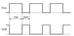
- FIG. 8 is an exemplary view illustrating an input waveform of the average detector 1 50 of FIGS. 6 and 7. As shown in the figure, the switch 53 repeats ON and OFF by the width of the output signal of the VCA or VCB.
- the LFP 52 of FIGS. 6 and 7 averages and outputs the width of the VCA or VCB, and transmits the same to the comparator 70 of FIG. 3, and the comparator 70 transmits the difference between the VCA and the VCB to the duty controller 10. To pass on.
- VoutB (I ⁇ Ton / C).
- VoutA VoutB.
- FIG. 9 is a configuration diagram of a second embodiment of a duty cycle correction device according to the present invention.
- the duty cycle correction apparatus As shown in the figure, the duty cycle correction apparatus according to the present invention, the duty regulator 10, buffer 1 (20), buffer 2 (30), inverter 40, average value detector 1 (50), average value detector 2 60, a comparator 70, and a duty ratio selector 80.
- the second embodiment of the duty cycle correction device of the present invention further includes a duty ratio selector 80 in the first embodiment described with reference to FIG. 3, and the description of other components is as described above. The description will be omitted.
- the duty ratio selector 80 selects the ratio of VCA and VCB, which are inputs of the comparator 70, and outputs the comparator 70 according to the ratio, thereby realizing a system having various duty ratios. Duty cycle compensation device can be designed.
- the pulse generator used in the conventional duty cycle correction device since the pulse generator used in the conventional duty cycle correction device is not used, the system can be miniaturized, and the power consumption can be reduced.
- the present invention does not use a delay device that generates an inherent delay error, so that the accuracy can be further increased.
Landscapes
- Physics & Mathematics (AREA)
- Nonlinear Science (AREA)
- Pulse Circuits (AREA)
- Manipulation Of Pulses (AREA)
Abstract
Description
본 발명은 듀티 사이클 보정장치에 관한 것이다.The present invention relates to a duty cycle correction device.
일반적으로, 듀티 사이클 보정기는, 디지털 시스템의 보정회로, 전원회로에 사용되는 스위칭 레귤레이터(Switching Regulator) 또는 신호동기 시스템의 지연동기루프 등에서 가장 널리 사용되는 회로 중 하나로서, 내부 또는 외부 클럭신호의 듀티 사이클을 보정하여, 정확한 데이터가 전달되도록 에러율을 감소시키는 역할을 하는 것이다.In general, the duty cycle compensator is one of the circuits most widely used in a correction circuit of a digital system, a switching regulator used in a power supply circuit, or a delayed synchronous loop of a signal synchronization system. By correcting the cycle, it serves to reduce the error rate so that accurate data is transmitted.
디지털 시스템에서는, 경로(path)지연과 반사경로에 의해 발생된 듀티 비율의 변화를 50%로 보정하여, 시스템의 샘플링(sampling) 신호가 정확하게 데이터를 검출할 수 있게 한다. 전원회로에 사용되는 스위칭 레귤레이터에서는, 스위치의 정확한 듀티 비율을 조절하여 성능을 향상시킨다. 또한, 지연동기루프에서는, 수신신호 데이터의 듀티 비율을 정확하게 조정 및 동기화하여 수신감도를 향상시킨다.In a digital system, the change in the duty ratio caused by the path delay and the reflection path is corrected to 50%, so that the sampling signal of the system can accurately detect the data. In switching regulators used in power circuits, the switch's exact duty ratio is adjusted to improve performance. Further, in the delay synchronization loop, the reception sensitivity is improved by accurately adjusting and synchronizing the duty ratio of the received signal data.
그러나, 종래의 듀티 사이클 보정기는, 펄스 발생기를 반드시 필요로 하므로, 정확한 펄스폭을 유지하기 위해 복잡한 회로가 요구되고, 듀티 사이클을 보정할 수 있는 범위가 제한적인 문제점이 있다. 또한, 종래의 듀티 사이클 보정기에서 사용되는 지연기는, 자체 고유의 지연오차를 가지고, 이러한 오차는 듀티 비율을 더욱 부정확하게 하는 문제점이 있다.However, since a conventional duty cycle corrector necessarily requires a pulse generator, a complicated circuit is required to maintain an accurate pulse width, and a range in which the duty cycle can be corrected is limited. In addition, the retarder used in the conventional duty cycle corrector has its own delay error, and this error has a problem of making the duty ratio more inaccurate.
본 발명이 해결하고자 하는 기술적 과제는, 펄스 발생기와 지연기를 사용하지 않아 자체 오차를 최소화하는 듀티 사이클 보정장치를 제공하는 것이다.The technical problem to be solved by the present invention is to provide a duty cycle correction device that minimizes its own error by not using a pulse generator and a delay.
본 발명이 해결하고자 하는 또 다른 기술적 과제는, 공정변화와 온도변화에 둔감하게 설계하여, 입력신호의 듀티 비율 변동에 따른 시스템 성능 저하를 최소화하는 듀티 사이클 보정장치를 제공하는 것이다.Another technical problem to be solved by the present invention is to provide a duty cycle correction device designed to be insensitive to process changes and temperature changes, thereby minimizing system performance degradation due to variation in the duty ratio of the input signal.
위와 같은 기술적 과제를 해결하기 위해, 입력신호의 듀티 비율을 보정하기 위한, 본 발명의 듀티 사이클 보정장치는, 상기 입력신호의 신호폭을 조정하는 조정부; 상기 조정부의 출력신호의 폭을 평균화하는 제1평균화부; 상기 조정부의 출력신호를 반전하는 인버터부; 상기 인버터부의 출력신호의 폭을 평균화하는 제2평균화부; 및 상기 제1 및 제2평균화부의 출력신호를 비교하고 그 차이를 출력하는 비교부를 포함한다.In order to solve the above technical problem, the duty cycle correction apparatus of the present invention for correcting the duty ratio of the input signal, the adjustment unit for adjusting the signal width of the input signal; A first averaging unit for averaging the widths of the output signals of the adjusting unit; An inverter unit for inverting an output signal of the adjustment unit; A second averaging unit for averaging the widths of the output signals of the inverter unit; And a comparing unit comparing the output signals of the first and second averaging units and outputting the difference.
본 발명의 일실시예에서, 상기 비교부의 출력을 이용하여 상기 조정부가 상기 입력신호의 폭을 조정할 수 있다.In one embodiment of the present invention, the adjustment unit may adjust the width of the input signal using the output of the comparison unit.
본 발명의 일실시예에서, 상기 제1평균화부 및 상기 제2평균화부의 출력신호의 비율을 선택하여, 상기 비교부가 해당 비율에 따라 차이를 출력하도록 하는 선택부를 더 포함할 수 있다.In one embodiment of the present invention, it may further include a selection unit for selecting the ratio of the output signal of the first averaged unit and the second averaged unit, so that the comparison unit outputs the difference according to the ratio.
본 발명의 일실시예에서, 상기 조정부의 출력을 일시적으로 저장하여 상기 제1평균화부로 출력하는 제1버퍼부를 더 포함할 수 있다.In one embodiment of the present invention, it may further include a first buffer unit for temporarily storing the output of the adjustment unit to output to the first averaging unit.
본 발명의 일실시예에서, 상기 인버터부는, 상기 제1버퍼부의 출력을 반전할 수 있다.In one embodiment of the present invention, the inverter unit may invert the output of the first buffer unit.
본 발명의 일실시예에서, 상기 제1버퍼부의 출력을 일시적으로 저장하여 출력하는 제2버퍼부를 더 포함할 수 있다.In one embodiment of the present invention, it may further include a second buffer unit for temporarily storing and outputting the output of the first buffer unit.
본 발명의 일실시예에서, 상기 조정부의 출력과 상기 인버터부의 출력의 듀티 비율이 일치되는 경우, 상기 비교부의 출력이 실질적으로 0이 될때까지, 상기 비교부의 출력이 상기 조정부로 입력될 수 있다.In one embodiment of the present invention, when the duty ratio of the output of the adjusting unit and the output of the inverter unit is matched, the output of the comparing unit may be input to the adjusting unit until the output of the comparing unit becomes substantially zero.
본 발명의 일실시예에서, 상기 조정부는, 입력신호의 폭을 상기 비교부의 출력에 의해 조절하는 조절부; 및 상기 조절부의 동작을 온/오프하는 제1스위치를 포함할 수 있다.In one embodiment of the present invention, the adjustment unit, the adjustment unit for adjusting the width of the input signal by the output of the comparison unit; And a first switch for turning on / off the control unit.
본 발명의 일실시예에서, 상기 제1평균화부 및 상기 제2평균화부는, 전류를 공급하는 전류원; 상기 전류원으로부터 공급되는 전류를 입력되는 전압의 하이/로우에 따라 스위칭하기 위한 제2스위치; 및 상기 제2스위치의 스위칭에 의해, 상기 전류원의 전류를 이용하여 입력되는 전압의 폭을 평균화하여 출력하는 저대역 통과필터(LPF)를 포함할 수 있다.In one embodiment of the present invention, the first and second averaging unit, the current source for supplying a current; A second switch for switching the current supplied from the current source according to the high / low of the input voltage; And a low pass filter (LPF) for averaging and outputting a width of the input voltage by using the current of the current source by switching of the second switch.
본 발명의 일실시예에서, 상기 LPF는 커패시터를 포함할 수 있다.In one embodiment of the present invention, the LPF may include a capacitor.
본 발명에 의하면, 종래의 듀티 사이클 보정장치에서 사용하던 펄스 발생기를 사용하지 않아, 시스템의 소형화가 가능하며, 전력소모를 줄일 수 있다.According to the present invention, since the pulse generator used in the conventional duty cycle correction device is not used, the system can be miniaturized and power consumption can be reduced.
또한, 본 발명은 고유의 지연오차를 발생하는 지연기를 사용하지 않아, 정밀도를 한층 높일 수 있다.In addition, the present invention does not use a delay device that generates an inherent delay error, thereby further increasing the accuracy.
도 1은 종래의 듀티 사이클 보정장치의 구성도이다.1 is a configuration diagram of a conventional duty cycle correction device.
도 2는 도 1의 각 노드에서의 신호 사이클을 설명하기 위한 도면이다.FIG. 2 is a diagram for describing a signal cycle at each node of FIG. 1.
도 3은 본 발명에 따른 듀티 사이클 보정장치의 일실시예 구성도이다.3 is a configuration diagram of an embodiment of a duty cycle correction device according to the present invention.
도 4a는 도 3의 듀티 조정기의 일실시예 상세 구성도이다.4A is a detailed block diagram of an embodiment of the duty adjuster of FIG. 3.
도 4b는 도 4a를 실제로 구현한 일실시예 회로도이다.FIG. 4B is a circuit diagram of an embodiment in which FIG. 4A is actually implemented.
도 5a는 도 3의 듀티 조정기의 다른 실시예 상세 구성도이다.5A is a detailed block diagram of another embodiment of the duty adjuster of FIG. 3.
도 5b는 도 5a를 실제로 구현한 일실시예 회로도이다.FIG. 5B is a circuit diagram of an embodiment in which FIG. 5A is actually implemented.
도 6 및 도 7은 도 3의 평균값 검출기의 일실시예 상세 구성도이다.6 and 7 are detailed configuration diagrams of an exemplary embodiment of the average value detector of FIG. 3.
도 8은 도 6 및 도 7의 평균값 검출기의 입력파형을 나타내는 일예시도이다.8 is an exemplary view illustrating input waveforms of the average detector of FIGS. 6 and 7.
도 9는 본 발명에 따른 듀티 사이클 보정장치의 제2실시예 구성도이다.9 is a configuration diagram of a second embodiment of a duty cycle correction device according to the present invention.
본 발명은 다양한 변경을 가할 수 있고 여러 가지 실시예를 가질 수 있는 바, 특정 실시예들을 도면에 예시하고 상세한 설명에 상세하게 설명하고자 한다.As the invention allows for various changes and numerous embodiments, particular embodiments will be illustrated in the drawings and described in detail in the written description.
그러나, 이는 본 발명을 특정한 실시 형태에 대해 한정하려는 것이 아니며, 본 발명의 사상 및 기술 범위에 포함되는 모든 변경, 균등물 내지 대체물을 포함하는 것으로 이해되어야 한다. However, this is not intended to limit the present invention to specific embodiments, it should be understood to include all modifications, equivalents, and substitutes included in the spirit and scope of the present invention.
제1, 제2 등과 같이 서수를 포함하는 용어는 다양한 구성요소를 설명하는데 사용될 수 있지만, 상기 구성요소는 상기 용어들에 의해 한정되지는 않는다.Terms including ordinal numbers such as first and second may be used to describe various components, but the components are not limited by the terms.
상기 용어들은 하나의 구성요소를 다른 구성요소로부터 구별하는 목적으로만 사용된다. 예를 들어, 본 발명의 권리 범위를 벗어나지 않으면서 제2 구성요소는 제1 구성요소로 명명될 수 있고, 유사하게 제1 구성요소도 제2 구성요소로 명명될 수 있다. The terms are used only for the purpose of distinguishing one component from another. For example, without departing from the scope of the present invention, the second component may be referred to as the first component, and similarly, the first component may also be referred to as the second component.
어떤 구성요소가 다른 구성요소에 "연결되어" 있다거나 "접속되어" 있다고 언급될 때에는, 그 다른 구성요소에 직접적으로 연결되어 있거나 또는 접속되어 있을 수도 있지만, 중간에 다른 구성요소가 존재할 수도 있다고 이해되어야 할 것이다. 반면에, 어떤 구성요소가 다른 구성요소에 "직접 연결되어" 있다거나 "직접 접속되어" 있다고 언급된 때에는, 중간에 다른 구성요소가 존재하지 않는 것으로 이해되어야 할 것이다.When a component is referred to as being "connected" or "connected" to another component, it may be directly connected or connected to that other component, but it may be understood that other components may be present in between. Should be. On the other hand, when a component is said to be "directly connected" or "directly connected" to another component, it should be understood that there is no other component in between.
본 출원에서 사용한 용어는 단지 특정한 실시예를 설명하기 위해 사용된 것으로, 본 발명을 한정하려는 의도가 아니다. 단수의 표현은 문맥상 명백하게 다르게 뜻하지 않는 한, 복수의 표현을 포함한다. The terminology used herein is for the purpose of describing particular example embodiments only and is not intended to be limiting of the present invention. Singular expressions include plural expressions unless the context clearly indicates otherwise.
본 출원에서, "포함한다" 또는 "가지다" 등의 용어는 명세서상에 기재된 특징, 숫자, 단계, 동작, 구성요소, 부품 또는 이들을 조합한 것이 존재함을 지정하려는 것이지, 하나 또는 그 이상의 다른 특징들이나 숫자, 단계, 동작, 구성요소, 부품 또는 이들을 조합한 것들의 존재 또는 부가 가능성을 미리 배제하지 않는 것으로 이해되어야 한다. In this application, the terms "comprises" or "having" are intended to indicate that there is a feature, number, step, operation, component, part, or combination thereof described in the specification, and one or more other features. It is to be understood that the present invention does not exclude the possibility of the presence or the addition of numbers, steps, operations, components, components, or a combination thereof.
또한 본 출원에서 첨부된 도면은 설명의 편의를 위하여 확대 또는 축소하여 도시된 것으로 이해되어야 한다. In addition, it is to be understood that the accompanying drawings in this application are shown enlarged or reduced for convenience of description.
이하에서는, 첨부된 도면을 참조로 하여, 종래의 듀티 사이클 보정장치를 설명하고, 이어, 본 발명의 듀티 사이클 보정장치를 상세히 설명하기로 한다.Hereinafter, with reference to the accompanying drawings, a conventional duty cycle correction device will be described, and then, the duty cycle correction device of the present invention will be described in detail.
도 1은 종래의 듀티 사이클 보정장치의 구성도이고, 도 2는 도 1의 각 노드에서의 신호 사이클을 설명하기 위한 도면이다.1 is a configuration diagram of a conventional duty cycle correction device, Figure 2 is a view for explaining the signal cycle at each node of FIG.
도면에 도시된 바와 같이, 종래의 듀티 사이클 보정기는, 펄스 발생기(100), 반주기 시간 지연기(110), 매칭 지연기(120) 및 SR 래치(Latch)(130)로 구성된다.As shown in the figure, a conventional duty cycle corrector is composed of a
도 1 및 도 2를 참조로 설명하면, 부정확한 듀티 비율을 가지는 입력신호 CK_in에 대해, 펄스 발생기(100)는 CK_in의 상승에지에서 펄스를 발생시킨다. Referring to FIGS. 1 and 2, for an input signal CK_in having an incorrect duty ratio, the
반주기 시간 지연기(110)는 펄스 발생기(100)의 반주기의 지연시간을 두어 반전신호를 발생시킨다. The half cycle
매칭 지연기(120)는 반주기 시간 지연기(110)의 고유한(intrinsic) 지연에 의해 발생된 오차를 보정하며, 펄스 발생기(100)에 대해 반전신호를 발생한다. The matching
SR 래치(130)는 반주기 시간 지연기(110)와 매칭 지연기(120)의 출력신호의 상승(rising) 또는 하강(falling) 순간에, 상승(rising) 또는 하강(falling)을 반복하여, 부정확한 듀티 비율을 가지는 신호 CK_in에 대하여 정확한 듀티 비율을 가지는 출력신호 CK_out을 출력한다.The
위와 같은 종래의 듀티 사이클 보정기는, 펄스 발생기(100)가 필요하므로, 정확한 펄스폭을 유지하기 위하여 회로가 복잡해지는 문제점이 있다. 또한, 입력신호 CK_in의 듀티 비율이 낮을 경우, 펄스 발생기(100)의 폭이 더욱 부정확하게 되어, 듀티 비율의 오차가 시간에 따라 변동하게 되어, 듀티 사이클을 보정할 수 있는 범위가 제한적인 문제점이 있다.The conventional duty cycle compensator as described above requires a
또한, 종래의 듀티 사이클 보정기는, 반주기 시간 지연기(110) 및 매칭 지연기(120)와 같은 지연기가 자체의 고유 지연오차를 가지고, 이러한 오차는 듀티 비율을 더욱 부정확하게 하는 문제점이 있다.In addition, the conventional duty cycle corrector has a problem in that delayers such as the half-
본 발명은 위와 같은 종래기술의 문제점을 해결하기 위하여, 듀티 사이클 보정장치의 설계에 있어, 펄스 발생기를 사용하지 않고, 또한 지연기에서 발생하는 고유의 지연오차를 최소화하기 위하여 지연기를 사용하지 않는다.In order to solve the above problems of the prior art, the present invention does not use a pulse generator in the design of a duty cycle correction device, and also does not use a delay to minimize inherent delay errors occurring in the delay device.
또한, 본 발명은, 공정변화와 온도변화에 둔감하도록 설계되었으며, 입력신호의 듀티 비율의 변동에 따른 시스템의 성능저하를 최소화한다. 또한, 최저 전력소모를 가능하게 하여, 본 발명의 듀티 사이클 보정장치를 더욱 다양한 분야에 적용할 수 있다. 이하, 본 발명의 듀티 사이클 보정장치를 상세하게 설명한다.In addition, the present invention is designed to be insensitive to process changes and temperature changes, and minimizes performance degradation of the system due to variation in the duty ratio of the input signal. In addition, by enabling the lowest power consumption, the duty cycle correction device of the present invention can be applied to more various fields. Hereinafter, the duty cycle correction device of the present invention will be described in detail.
도 3은 본 발명에 따른 듀티 사이클 보정장치의 일실시예 구성도이다.3 is a configuration diagram of an embodiment of a duty cycle correction device according to the present invention.
도면에 도시된 바와 같이, 본 발명의 보정장치는, 듀티 조정기(Duty-Alert Clock)(10), 버퍼(Buffer)1(20), 버퍼2(30), 인버터(Inverter)(40), 평균값 검출기(Average Value Detector)1(50), 평균값 검출기2(60) 및 비교기(Comparator)(70)를 포함한다.As shown in the figure, the correction apparatus of the present invention, a duty-alert clock (10), a buffer (Buffer) 1 (20), a buffer 2 (30), an inverter (Inverter 40), the average value An average value detector 1 (50), an average value detector 2 (60), and a
듀티 조정기(10)는, 부정확한 듀티 비율을 가지는 입력신호 CK가 입력되면, 비교기(70)에서 검출된 출력신호 Verr의 크기에 의해 신호폭을 조정한다.The
버퍼1(20)은 듀티 조정기(10)의 출력을 일시로 저장하였다가 출력하고, 버퍼2(30)는 버퍼1(20)의 출력을 일시로 저장하였다가 출력한다. 버퍼2(20)의 출력은 듀티 조정기(10)의 출력의 확인을 위한 신호로 사용될 수 있다.The
평균값 검출기1(50)는 듀티 조정기(10)의 출력 VCA의 폭을 평균화한다.The
인버터(40)는 버퍼1(20)의 출력을 반전하여 VCB를 출력한다.The
평균값 검출기2(60)는, 인버터(40)의 출력 VCB의 폭을 평균화한다.The average value detector 2 60 averages the width of the output VCB of the
평균값 검출기1(50)과 평균값 검출기2(60)의 출력 VoutA, VoutB는 다시 비교기(70)가 비교하여, 비교한 출력을 듀티 조정기(10)에 제공한다.The outputs VoutA and VoutB of the
이를 신호의 흐름으로 설명하면, 듀티 조정기(10)에 부정확한 듀티 비율을 가지는 입력신호 CK가 입력되면, 비교기(70)에서 검출된 출력 Verr의 크기에 의해 입력신호의 폭이 조절되고, 그 출력 VCA는 평균값 검출기1(50)에 의해 평균화되고, 인버터(40)에 의해 반전된 신호 VCB는 평균값 검출기2(60)에서 평균화되어, 다시 비교기(70)에서 재비교된다.When this is described as a signal flow, when the input signal CK having an incorrect duty ratio is input to the
이러한 과정은, VCA와 VCB의 듀티 비율이 완전히 일치되는 50% 듀티 비율의 시스템에서는, 비교기(70)에서 검출된 출력신호 Verr가 영(zero)이 될 때까지 반복된다. 이러한 과정을 통해 본 발명의 듀티 사이클 보정장치는, 펄스 발생기나 지연기 등을 사용하지 않아도, 정확하게 듀티 비율을 조절할 수 있다.This process is repeated until the output signal Verr detected by the
도 4a 및 도 5a는 각각 도 3의 듀티 조정기의 일실시예 상세 구성도이며, 도 4b는 도 4a를, 도 5b는 도 5a를 실제로 구현한 일실시예 회로도이다.4A and 5A are detailed diagrams showing one embodiment of the duty regulator of FIG. 3, respectively, and FIG. 4B is a circuit diagram of an embodiment of FIG. 4A and FIG. 5B.
도 4a 및 도 5a에 도시된 바와 같이, 본 발명의 듀티 사이클 보정장치의 듀티 조정기(10)는, 조절기(12)의 동작을 온/오프하는 스위치(SW)(11)와 전압 또는 전류를 조절하는 조절기(12)를 포함한다. 도 4a 및 도 5a에서는, 그 구성은 동일하지만, 그 배치가 다른 예가 도시되어 있는 것이다.As shown in FIGS. 4A and 5A, the
조절기(12)는 각각, 입력신호 CK의 폭을, 비교기 출력 Verr에 의해 조절한다. The
도 4a 및 도 5a의 실제 구현예는, 각각 도 4b 및 도 5b와 같으며, 본 발명의 일실시예에서, 트랜지스터 Mp는 스위치(11)로, 트랜지스터 Mn은 조절기(12)로 각각 사용되었다.4A and 5A are the same as in FIGS. 4B and 5B, respectively, and in one embodiment of the invention, transistor Mp is used as
도 6 및 도 7은 도 3의 평균값 검출기의 일실시예 상세 구성도로서, 도 3의 평균값 검출기1(50) 및 평균값 검출기2(60) 모두 동일하게 구성될 수 있을 것이다. 설명의 편의를 위하여, 평균값 검출기1(50)의 경우를 예를 들어 설명하기로 하겠으나, 평균값 검출기2(60)를 본 발명의 설명에서 배제하는 것은 아니다.6 and 7 are detailed diagrams of an exemplary embodiment of the average detector of FIG. 3, and the
도 6 및 도 7에 도시된 바와 같이, 본 발명의 보정장치의 평균값 검출기1(50)은, 전류원(51), 저대역 통과 필터(Low Pass Filter; LPF)(52) 및 스위치(53)를 포함한다. 도 6과 도 7에서는, 구성은 동일하지만, 그 배치가 다른 예가 도시되어 있다. LPF(52)는 캐패시터(capacitor)로 대체될 수도 있다.As shown in Figs. 6 and 7, the average detector 1 (50) of the compensator of the present invention uses a
도 8은 도 6 및 도 7의 평균값 검출기1(50)의 입력파형을 나타내는 일예시도이다. 도면에 도시된 바와 같이, VCA 또는 VCB의 출력신호의 폭만큼, 스위치(53)는 온(ON)과 오프(OFF)를 반복한다. FIG. 8 is an exemplary view illustrating an input waveform of the
도 6의 평균값 검출기1(50)에서는, 스위치(53)가 온(ON)인 경우에 충전되고, 오프(OFF)인 경우에 방전된다. 도 7의 경우에는 위와 반대이다.In the
도 6 및 도 7의 LFP(52)는 VCA 또는 VCB의 폭을 평균화하여 출력하여, 이를 도 3의 비교기(70)로 전달하며, 비교기(70)는 VCA와 VCB의 차를 듀티 조정기(10)에 전달한다.The
이와 같은 과정을, 비교기(70)의 출력이 0이 될 때까지 반복수행하여, 안정적인 듀티 비율을 발생하도록 하는 것임은, 이미 설명한 바와 같다.This process is repeated until the output of the
즉, 도 6에서, VCA가 하이(HIGH)이면 스위치(53)는 온(ON)이고, 전류원(51)의 전류는 접지(GND)로 흐르고, LPF(52)의 내부 캐패시터의 전하는 방전된다. 반대로, VCA가 로우(LOW)이면, 스위치(53)는 오프(OFF)이고, 전류원(51)의 전류 I는 LPF(52)의 내부 캐패시터에 전하 Q를 Q=C×VoutA 만큼 오프(OFF)시간동안 충전한다(C는 LPF(52)의 내부 캐패시터의 캐패시턴스임). 이는 Q=I×Toff로 표현될 수 있다. 따라서, VoutA=(I×Toff/C)가 된다. That is, in FIG. 6, when VCA is HIGH, the
도 7과 같은 구성에서는 도 6과 온(ON)/오프(OFF) 동작이 반대가 되고, VoutB=(I×Ton/C)로 표현될 수 있다.In the configuration shown in FIG. 7, the on / off operation of FIG. 6 is reversed and may be expressed as VoutB = (I × Ton / C).
50%의 듀티 비율을 가지는 시스템에서는 VoutA=VoutB이다.In a system with a 50% duty ratio, VoutA = VoutB.
도 9는 본 발명에 따른 듀티 사이클 보정장치의 제2실시예 구성도이다.9 is a configuration diagram of a second embodiment of a duty cycle correction device according to the present invention.
도면에 도시된 바와 같이, 본 발명에 따른 듀티 사이클 보정장치는, 듀티 조정기(10), 버퍼1(20), 버퍼2(30), 인버터(40), 평균값 검출기1(50), 평균값 검출기2(60), 비교기(70) 및 듀티 비율 선택기(Duty Ratio Selector)(80)를 포함한다. 본 발명의 듀티 사이클 보정장치의 제2실시예는, 도 3에서 설명한 제1실시예에서 듀티 비율 선택기(80)를 더 포함하는 것으로서, 그 외의 구성요소의 설명에 대해서는 이미 설명한 바와 같으므로, 그에 대한 설명은 생략하는 것으로 하겠다.As shown in the figure, the duty cycle correction apparatus according to the present invention, the
듀티 비율 선택기(80)는 비교기(70)의 입력인 VCA와 VCB의 비율을 선택하여 비교기(70)가 해당 비율에 따라 출력하도록 하는 것으로서, 이에 의해 다양한 듀티 비율을 가지는 시스템을 구현할 수 있으며, 정교한 듀티 사이클 보정장치를 설계할 수 있다.The
본 발명에 의하면, 종래의 듀티 사이클 보정장치에서 사용하던 펄스 발생기를 사용하지 않아, 시스템의 소형화가 가능하게 하는 효과가 있으며, 전력소모를 줄일 수 있도록 하는 효과가 있다.According to the present invention, since the pulse generator used in the conventional duty cycle correction device is not used, the system can be miniaturized, and the power consumption can be reduced.
또한, 본 발명은 고유의 지연오차를 발생하는 지연기를 사용하지 않아, 정밀도를 한층 높일 수 있어, 디지털 및 아날로그 시스템, 전원회로, 동기회로뿐 아니라, 높은 집적도가 요구되고 저전력 소모가 요구되는 센서나 무선인식(RFID) 태그 등에도 사용될 수 있을 것이다.In addition, the present invention does not use a delay device that generates an inherent delay error, so that the accuracy can be further increased. As well as a digital and analog system, a power supply circuit, a synchronization circuit, a sensor that requires high integration and low power consumption, It may also be used for RFID tags.
이상에서 본 발명에 따른 실시예들이 설명되었으나, 이는 예시적인 것에 불과하며, 당해 분야에서 통상적 지식을 가진 자라면 이로부터 다양한 변형 및 균등한 범위의 실시예가 가능하다는 점을 이해할 것이다. 따라서, 본 발명의 진정한 기술적 보호 범위는 다음의 특허청구범위에 의해서 정해져야 할 것이다.Although embodiments according to the present invention have been described above, these are merely exemplary, and it will be understood by those skilled in the art that various modifications and equivalent embodiments of the present invention are possible therefrom. Therefore, the true technical protection scope of the present invention will be defined by the following claims.
Claims (10)
Priority Applications (2)
| Application Number | Priority Date | Filing Date | Title |
|---|---|---|---|
| CN201280031276.5A CN103620961A (en) | 2011-06-24 | 2012-06-25 | Duty cycle correction apparatus |
| US14/127,876 US20140125391A1 (en) | 2011-06-24 | 2012-06-25 | Duty cycle correction apparatus |
Applications Claiming Priority (2)
| Application Number | Priority Date | Filing Date | Title |
|---|---|---|---|
| KR1020110061881A KR101309465B1 (en) | 2011-06-24 | 2011-06-24 | Apparatus for correcting duty cycle |
| KR10-2011-0061881 | 2011-06-24 |
Publications (2)
| Publication Number | Publication Date |
|---|---|
| WO2012177101A2 true WO2012177101A2 (en) | 2012-12-27 |
| WO2012177101A3 WO2012177101A3 (en) | 2013-03-28 |
Family
ID=47423123
Family Applications (1)
| Application Number | Title | Priority Date | Filing Date |
|---|---|---|---|
| PCT/KR2012/004999 Ceased WO2012177101A2 (en) | 2011-06-24 | 2012-06-25 | Duty cycle correction apparatus |
Country Status (4)
| Country | Link |
|---|---|
| US (1) | US20140125391A1 (en) |
| KR (1) | KR101309465B1 (en) |
| CN (1) | CN103620961A (en) |
| WO (1) | WO2012177101A2 (en) |
Cited By (1)
| Publication number | Priority date | Publication date | Assignee | Title |
|---|---|---|---|---|
| CN104716930A (en) * | 2013-12-12 | 2015-06-17 | 国际商业机器公司 | System and method for adjusting duty cycle for preventing error spread |
Families Citing this family (7)
| Publication number | Priority date | Publication date | Assignee | Title |
|---|---|---|---|---|
| US9492741B2 (en) | 2013-05-22 | 2016-11-15 | Microsoft Technology Licensing, Llc | Wireless gaming protocol |
| JP2015012352A (en) * | 2013-06-27 | 2015-01-19 | マイクロン テクノロジー, インク. | Semiconductor device |
| US10447247B1 (en) * | 2018-04-27 | 2019-10-15 | Sandisk Technologies Llc | Duty cycle correction on an interval-by-interval basis |
| CN110957998B (en) * | 2019-12-02 | 2020-08-11 | 翱捷智能科技(上海)有限公司 | Circuit for accurately correcting duty ratio of clock signal |
| US11527195B2 (en) * | 2021-04-22 | 2022-12-13 | Novatek Microelectronics Corp. | Display control system and related method of signal transmission |
| US11509296B2 (en) * | 2021-04-25 | 2022-11-22 | Novatek Microelectronics Corp. | Clock generator for frequency multiplication |
| US11671085B2 (en) | 2021-11-01 | 2023-06-06 | Nxp B.V. | Circuit to correct duty cycle and phase error of a differential signal with low added noise |
Family Cites Families (7)
| Publication number | Priority date | Publication date | Assignee | Title |
|---|---|---|---|---|
| KR100525080B1 (en) | 1999-02-05 | 2005-11-01 | 매그나칩 반도체 유한회사 | Average duty cycle corrector |
| US7019574B2 (en) * | 2004-01-29 | 2006-03-28 | Schroedinger Karl | Circuit and method for correction of the duty cycle value of a digital data signal |
| US7005904B2 (en) | 2004-04-30 | 2006-02-28 | Infineon Technologies Ag | Duty cycle correction |
| TWI304293B (en) * | 2005-12-23 | 2008-12-11 | Ind Tech Res Inst | Duty cycle corrector circuit with widely operating range |
| KR101050406B1 (en) * | 2008-09-22 | 2011-07-19 | 주식회사 하이닉스반도체 | Duty Correction Circuit and Clock Generation Circuit Including It |
| KR100918263B1 (en) | 2008-11-04 | 2009-09-21 | 주식회사 파이칩스 | Duty Cycle Compensator |
| JP5231289B2 (en) * | 2009-03-02 | 2013-07-10 | ルネサスエレクトロニクス株式会社 | Duty ratio correction circuit and duty ratio correction method |
-
2011
- 2011-06-24 KR KR1020110061881A patent/KR101309465B1/en not_active Expired - Fee Related
-
2012
- 2012-06-25 CN CN201280031276.5A patent/CN103620961A/en active Pending
- 2012-06-25 US US14/127,876 patent/US20140125391A1/en not_active Abandoned
- 2012-06-25 WO PCT/KR2012/004999 patent/WO2012177101A2/en not_active Ceased
Cited By (4)
| Publication number | Priority date | Publication date | Assignee | Title |
|---|---|---|---|---|
| CN104716930A (en) * | 2013-12-12 | 2015-06-17 | 国际商业机器公司 | System and method for adjusting duty cycle for preventing error spread |
| US20150171834A1 (en) * | 2013-12-12 | 2015-06-18 | International Business Machines Corporation | Duty cycle adjustment with error resiliency |
| US9306547B2 (en) * | 2013-12-12 | 2016-04-05 | International Business Machines Corporation | Duty cycle adjustment with error resiliency |
| CN104716930B (en) * | 2013-12-12 | 2018-02-02 | 国际商业机器公司 | System and method for the dutycycle adjustment with error resiliency |
Also Published As
| Publication number | Publication date |
|---|---|
| US20140125391A1 (en) | 2014-05-08 |
| WO2012177101A3 (en) | 2013-03-28 |
| KR101309465B1 (en) | 2013-09-23 |
| KR20130001023A (en) | 2013-01-03 |
| CN103620961A (en) | 2014-03-05 |
Similar Documents
| Publication | Publication Date | Title |
|---|---|---|
| WO2012177101A2 (en) | Duty cycle correction apparatus | |
| WO2011065685A2 (en) | Oscillator circuit which compensates for external voltage supply, temperature and process | |
| WO2011021808A2 (en) | Adaptive equalization apparatus and equalization method | |
| WO2010027222A4 (en) | Amplifier including dithering switch, and display driving circuit using the amplifier | |
| WO2020111896A1 (en) | Device and method for measuring battery cell resistance | |
| KR101434057B1 (en) | Phase shift circuit and power factor correction circuit including the same | |
| WO2011037292A1 (en) | Time domain voltage comparator of analog-digital converter | |
| WO2014069873A1 (en) | Switch relay apparatus | |
| WO2018128216A1 (en) | Multi-channel switching converter | |
| CN106658868B (en) | A kind of LED drive device and its line voltage compensation circuit and compensation method | |
| WO2022080624A1 (en) | Adaptive soft-start and soft-stop device for converter | |
| WO2017122960A1 (en) | Doorbell device and method for supplying power thereto | |
| WO2014148706A1 (en) | Apparatus for discriminating type of analog sensor | |
| WO2019172467A1 (en) | Phase-locked loop apparatus and method for clock synchronization | |
| WO2024128479A1 (en) | Clock duty calibration device and method | |
| WO2016047964A1 (en) | Alternating-current led drive circuit | |
| WO2017164502A1 (en) | Direct current voltage function calibration device and method | |
| WO2015072679A1 (en) | Device and method for controlling output amplitude of voltage control oscillator in electronic device | |
| WO2018093073A1 (en) | Cooking vessel detection apparatus, cooking vessel detection method, and induction heating cooker | |
| WO2011152589A1 (en) | Signal processing apparatus and signal processing method thereof | |
| WO2009145458A9 (en) | Parallel connected switching converter using charge sharing | |
| WO2014104808A1 (en) | Charge pump apparatus | |
| KR101930324B1 (en) | Duty cycle corrector | |
| WO2024191162A2 (en) | Pulse dc power source supply for capacitive load, and operating method therefor | |
| WO2016032028A1 (en) | Method for testing battery protection circuit and apparatus therefor |
Legal Events
| Date | Code | Title | Description |
|---|---|---|---|
| 121 | Ep: the epo has been informed by wipo that ep was designated in this application |
Ref document number: 12801808 Country of ref document: EP Kind code of ref document: A2 |
|
| WWE | Wipo information: entry into national phase |
Ref document number: 14127876 Country of ref document: US |
|
| NENP | Non-entry into the national phase |
Ref country code: DE |
|
| 122 | Ep: pct application non-entry in european phase |
Ref document number: 12801808 Country of ref document: EP Kind code of ref document: A2 |