WO2013011955A1 - 遅延蛍光材料およびそれを用いた有機エレクトロルミネッセンス素子 - Google Patents
遅延蛍光材料およびそれを用いた有機エレクトロルミネッセンス素子 Download PDFInfo
- Publication number
- WO2013011955A1 WO2013011955A1 PCT/JP2012/067970 JP2012067970W WO2013011955A1 WO 2013011955 A1 WO2013011955 A1 WO 2013011955A1 JP 2012067970 W JP2012067970 W JP 2012067970W WO 2013011955 A1 WO2013011955 A1 WO 2013011955A1
- Authority
- WO
- WIPO (PCT)
- Prior art keywords
- group
- general formula
- electron
- ring
- fluorescent material
- Prior art date
- Legal status (The legal status is an assumption and is not a legal conclusion. Google has not performed a legal analysis and makes no representation as to the accuracy of the status listed.)
- Ceased
Links
Images


Classifications
-
- H—ELECTRICITY
- H10—SEMICONDUCTOR DEVICES; ELECTRIC SOLID-STATE DEVICES NOT OTHERWISE PROVIDED FOR
- H10K—ORGANIC ELECTRIC SOLID-STATE DEVICES
- H10K85/00—Organic materials used in the body or electrodes of devices covered by this subclass
- H10K85/60—Organic compounds having low molecular weight
- H10K85/615—Polycyclic condensed aromatic hydrocarbons, e.g. anthracene
- H10K85/624—Polycyclic condensed aromatic hydrocarbons, e.g. anthracene containing six or more rings
-
- H—ELECTRICITY
- H10—SEMICONDUCTOR DEVICES; ELECTRIC SOLID-STATE DEVICES NOT OTHERWISE PROVIDED FOR
- H10K—ORGANIC ELECTRIC SOLID-STATE DEVICES
- H10K85/00—Organic materials used in the body or electrodes of devices covered by this subclass
- H10K85/60—Organic compounds having low molecular weight
- H10K85/649—Aromatic compounds comprising a hetero atom
- H10K85/654—Aromatic compounds comprising a hetero atom comprising only nitrogen as heteroatom
-
- H—ELECTRICITY
- H10—SEMICONDUCTOR DEVICES; ELECTRIC SOLID-STATE DEVICES NOT OTHERWISE PROVIDED FOR
- H10K—ORGANIC ELECTRIC SOLID-STATE DEVICES
- H10K50/00—Organic light-emitting devices
-
- C—CHEMISTRY; METALLURGY
- C07—ORGANIC CHEMISTRY
- C07C—ACYCLIC OR CARBOCYCLIC COMPOUNDS
- C07C255/00—Carboxylic acid nitriles
- C07C255/49—Carboxylic acid nitriles having cyano groups bound to carbon atoms of six-membered aromatic rings of a carbon skeleton
- C07C255/58—Carboxylic acid nitriles having cyano groups bound to carbon atoms of six-membered aromatic rings of a carbon skeleton containing cyano groups and singly-bound nitrogen atoms, not being further bound to other hetero atoms, bound to the carbon skeleton
-
- C—CHEMISTRY; METALLURGY
- C07—ORGANIC CHEMISTRY
- C07D—HETEROCYCLIC COMPOUNDS
- C07D209/00—Heterocyclic compounds containing five-membered rings, condensed with other rings, with one nitrogen atom as the only ring hetero atom
- C07D209/56—Ring systems containing three or more rings
- C07D209/80—[b, c]- or [b, d]-condensed
- C07D209/82—Carbazoles; Hydrogenated carbazoles
- C07D209/86—Carbazoles; Hydrogenated carbazoles with only hydrogen atoms, hydrocarbon or substituted hydrocarbon radicals, directly attached to carbon atoms of the ring system
-
- C—CHEMISTRY; METALLURGY
- C07—ORGANIC CHEMISTRY
- C07D—HETEROCYCLIC COMPOUNDS
- C07D519/00—Heterocyclic compounds containing more than one system of two or more relevant hetero rings condensed among themselves or condensed with a common carbocyclic ring system not provided for in groups C07D453/00 or C07D455/00
-
- C—CHEMISTRY; METALLURGY
- C09—DYES; PAINTS; POLISHES; NATURAL RESINS; ADHESIVES; COMPOSITIONS NOT OTHERWISE PROVIDED FOR; APPLICATIONS OF MATERIALS NOT OTHERWISE PROVIDED FOR
- C09K—MATERIALS FOR MISCELLANEOUS APPLICATIONS, NOT PROVIDED FOR ELSEWHERE
- C09K11/00—Luminescent materials, e.g. electroluminescent or chemiluminescent
- C09K11/06—Luminescent materials, e.g. electroluminescent or chemiluminescent containing organic luminescent materials
-
- H—ELECTRICITY
- H05—ELECTRIC TECHNIQUES NOT OTHERWISE PROVIDED FOR
- H05B—ELECTRIC HEATING; ELECTRIC LIGHT SOURCES NOT OTHERWISE PROVIDED FOR; CIRCUIT ARRANGEMENTS FOR ELECTRIC LIGHT SOURCES, IN GENERAL
- H05B33/00—Electroluminescent light sources
- H05B33/12—Light sources with substantially two-dimensional [2D] radiating surfaces
- H05B33/14—Light sources with substantially two-dimensional [2D] radiating surfaces characterised by the chemical or physical composition or the arrangement of the electroluminescent material, or by the simultaneous addition of the electroluminescent material in or onto the light source
-
- H—ELECTRICITY
- H10—SEMICONDUCTOR DEVICES; ELECTRIC SOLID-STATE DEVICES NOT OTHERWISE PROVIDED FOR
- H10K—ORGANIC ELECTRIC SOLID-STATE DEVICES
- H10K50/00—Organic light-emitting devices
- H10K50/10—OLEDs or polymer light-emitting diodes [PLED]
- H10K50/11—OLEDs or polymer light-emitting diodes [PLED] characterised by the electroluminescent [EL] layers
-
- C—CHEMISTRY; METALLURGY
- C09—DYES; PAINTS; POLISHES; NATURAL RESINS; ADHESIVES; COMPOSITIONS NOT OTHERWISE PROVIDED FOR; APPLICATIONS OF MATERIALS NOT OTHERWISE PROVIDED FOR
- C09K—MATERIALS FOR MISCELLANEOUS APPLICATIONS, NOT PROVIDED FOR ELSEWHERE
- C09K2211/00—Chemical nature of organic luminescent or tenebrescent compounds
- C09K2211/10—Non-macromolecular compounds
- C09K2211/1003—Carbocyclic compounds
- C09K2211/1011—Condensed systems
-
- H—ELECTRICITY
- H10—SEMICONDUCTOR DEVICES; ELECTRIC SOLID-STATE DEVICES NOT OTHERWISE PROVIDED FOR
- H10K—ORGANIC ELECTRIC SOLID-STATE DEVICES
- H10K85/00—Organic materials used in the body or electrodes of devices covered by this subclass
- H10K85/60—Organic compounds having low molecular weight
- H10K85/649—Aromatic compounds comprising a hetero atom
- H10K85/657—Polycyclic condensed heteroaromatic hydrocarbons
- H10K85/6572—Polycyclic condensed heteroaromatic hydrocarbons comprising only nitrogen in the heteroaromatic polycondensed ring system, e.g. phenanthroline or carbazole
Definitions
- the present invention relates to a novel delayed fluorescent material having high luminous efficiency and an organic electroluminescence element (organic EL element) using the same for a light emitting layer.
- Patent Document 1 describes a phosphorescent organic electroluminescence device using a compound having a spirobifluorene skeleton in a hole blocking layer.
- Patent Document 2 describes an organic electroluminescence device using a compound having a spirobifluorene skeleton having two carbazole groups bonded as a host material of a light emitting layer.
- Patent Document 3 describes an organic electroluminescence device using a phenyl vinyl group or a compound having a spirobifluorene skeleton substituted with a phenyl group as a host material of a light emitting layer.
- Patent Document 4 describes an organic electroluminescence device having a light-emitting layer composed only of a compound having a spirobifluorene skeleton substituted with a biphenyl group.
- Patent Document 5 describes an organic electroluminescence device having a light emitting layer composed of only a benzene or naphthalene compound substituted with 1 to 3 spirobifluorene rings.
- Patent Document 6 describes an organic electroluminescence device having a light emitting layer composed only of a benzene compound substituted with 3 to 6 spirobifluorene rings.
- a compound having a spirobifluorene skeleton is not always easy to synthesize, it may be difficult to provide the compound itself.
- the present inventors have synthesized various compounds having a spirobifluorene skeleton and studied for the purpose of evaluating the usefulness of the organic electroluminescence device as a light emitting material in detail. Proceeded.
- a general formula of a compound useful as a light-emitting material has been derived, and extensive studies have been carried out for the purpose of generalizing the structure of an organic electroluminescence device having high luminous efficiency.
- the present inventors have found that a specific compound having a spirobifluorene skeleton has excellent properties as a delayed fluorescent material for an organic electroluminescence device. . Based on this finding, the present inventors have provided the following present invention as means for solving the above-mentioned problems.
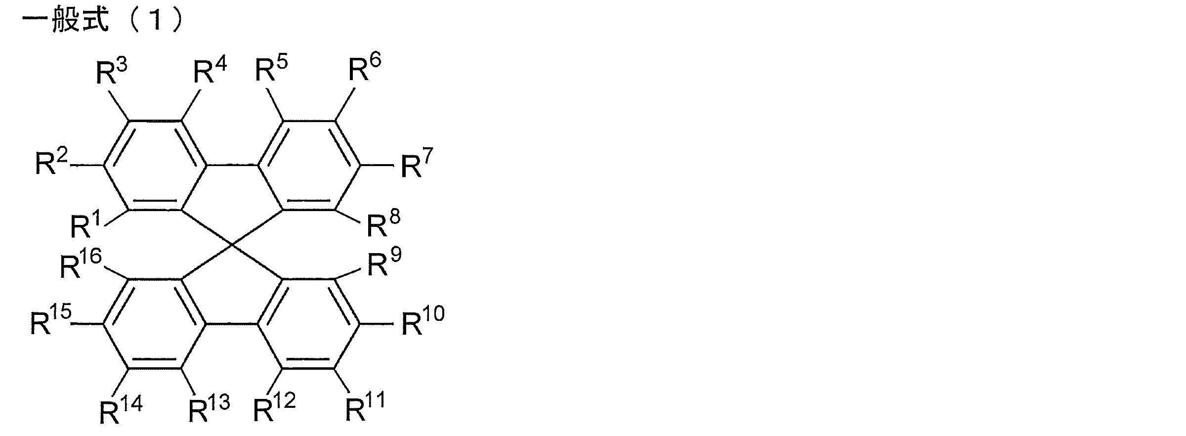
- a delayed fluorescent material comprising a compound represented by the following general formula (1).
- R 1 , R 2 , R 3 , R 4 , R 5 , R 6 , R 7 and R 8 are each independently a hydrogen atom or an electron-donating group, and at least one of Represents an electron donating group.
- R 9 , R 10 , R 11 , R 12 , R 13 , R 14 , R 15 and R 16 are each independently a hydrogen atom or an electron withdrawing group, and at least one represents an electron withdrawing group.
- At least two of R 1 , R 2 , R 3 , R 4 , R 5 , R 6 , R 7 and R 8 in the general formula (1) are electron donating groups
- At least one of R 1 , R 2 , R 3 and R 4 in the general formula (1) is an electron donating group, and at least one of R 5 , R 6 , R 7 and R 8 is an electron donating group.
- the delayed fluorescent material according to [1] which is characterized in that it exists.
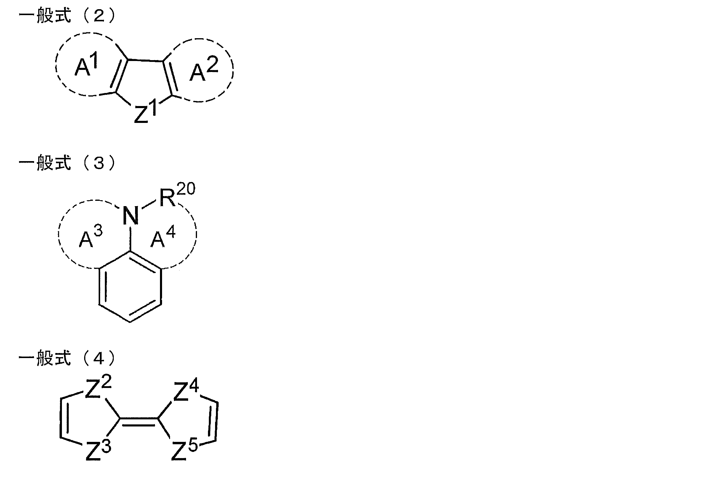
- R 1 , R 2 , R 3 , R 4 , R 5 , R 6 , R 7 and R 8 is a skeleton represented by any one of the following general formulas (2) to (4)
- R 20 represents an atomic group necessary to form a ring structure represented by a hydrogen atom, an aryl group, or A 4, each independently as A 3 and A 4, heteroaromatic ring, or A non-aromatic heterocycle may be formed.
- Z 1 , Z 2 , Z 3 and Z 4 each independently represent an oxygen atom or a sulfur atom.
- At least one of R 1 , R 2 , R 3 , R 4 , R 5 , R 6 , R 7 and R 8 is an electron donating group containing any one of the following skeletons of D1 to D10
- R 9 , R 10 , R 11 , R 12 , R 13 , R 14 , R 15 and R 16 are electron withdrawing groups
- the delayed fluorescent material according to any one of [8].
- At least one of R 9 , R 10 , R 11 and R 12 in the general formula (1) is an electron withdrawing group, and at least one of R 13 , R 14 , R 15 and R 16 is an electron withdrawing group.
- An organic electroluminescence device having an anode, a cathode, and at least one organic layer including a light-emitting layer between the anode and the cathode, wherein the organic electroluminescence element is any one of [1] to [12]
- An organic electroluminescent device comprising the light-emitting layer containing the delayed fluorescent material.
- R 1 , R 2 , R 3 , R 4 , R 5 , R 6 , R 7 and R 8 are each independently a hydrogen atom or an electron-donating group, and at least one Represents an electron-donating group containing a skeleton represented by any one of the above general formulas (2) to (4).
- R 9 , R 10 , R 11 , R 12 , R 13 , R 14 , R 15 and R 16 are each independently a hydrogen atom or an electron withdrawing group, and at least one represents an electron withdrawing group.
- At least one of R 1 , R 2 , R 3 , R 4 , R 5 , R 6 , R 7 and R 8 is an electron donating group containing a skeleton represented by any one of the above D1 to D8
- the compound according to [14] which is characterized in that [16] At least one of R 1 , R 2 , R 3 , R 4 , R 5 , R 6 , R 7 and R 8 is an electron donating group containing a skeleton represented by D9 [ 15].
- the delayed fluorescent material of the present invention is the first delayed fluorescent material having a spirobifluorene skeleton.
- an organic electroluminescence device having high light emission efficiency can be provided.
- Example 2 is an emission spectrum of a co-deposited film in Example 1.
- 3 is a graph showing PL transient attenuation in Example 1.
- 2 is an emission spectrum of the organic electroluminescence element in Example 1.
- 3 is a graph showing the relationship between temperature and luminous efficiency in Example 1.
- 6 is a graph showing the relationship between the intensity ratio of long-life light emission to single-life light emission and the reciprocal of temperature in Example 1.
- 3 is a graph showing the relationship between current density and external quantum efficiency in Example 1.
- 3 is a graph showing current density-voltage-luminance (J-V-L) characteristics in Example 1. It is an emission spectrum of the solution in Example 42.
- 42 is a graph showing PL transient attenuation in Example 42.
- 42 is a graph showing PL transient attenuation in Example 43.
- a numerical range represented by using “to” means a range including numerical values described before and after “to” as a lower limit value and an upper limit value.
- the delayed fluorescent material of the present invention is characterized by comprising a compound represented by the following general formula (1). Therefore, first, the compound represented by the general formula (1) will be described.
- R 1 , R 2 , R 3 , R 4 , R 5 , R 6 , R 7 and R 8 in the general formula (1) each independently represent a hydrogen atom or an electron donating group. However, at least one of these represents an electron donating group. When two or more of these represent an electron donating group, the two or more electron donating groups may be the same or different. Preferred is the case where they are identical.
- R 1 , R 2 , R 3 , R 4 , R 5 , R 6 , R 7 and R 8 those representing an electron donating group are R 2 , R 3 , R 4 , R 5 , R 6 and R 7.
- the electron donating groups represented by R 1 , R 2 , R 3 , R 4 , R 5 , R 6 , R 7 and R 8 donate electrons to the spirobifluorene ring when bonded to the spirobifluorene ring. It is a group having properties.
- the electron donating group may be an aromatic group, a heteroaromatic group, or an aliphatic group, or may be a group in which two or more of these are combined.
- Examples of the electron donor group may be an alkyl group (which may be linear, branched or cyclic, preferably have 1 to 6 carbon atoms, more preferably 1 to 3 carbon atoms, As a methyl group, an ethyl group, a propyl group, a pentyl group, a hexyl group, and an isopropyl group) or an alkoxy group (straight, branched, or cyclic), preferably 1 carbon atom 6 or more, more preferably 1 to 3 carbon atoms, and specific examples include a methoxy group), an amino group or a substituted amino group (preferably an amino group substituted with an aromatic group, Examples include diphenylamino group, anilyl group, and tolylamino group), aryl group (which may be monocyclic or fused ring, and may be further substituted with aryl group.
- alkyl group which may be linear, branched or cyclic, preferably have 1 to 6 carbon atoms, more
- An electron donating group containing a heterocyclic structure preferably an electron donating group containing a heterocyclic structure containing a nitrogen atom or a sulfur atom.
- Specific examples thereof include thiophenyl.
- the electron donating group preferably has a ⁇ p value of ⁇ 0.06 or less, more preferably ⁇ 0.14 or less, and even more preferably ⁇ 0.28 or less.
- At least one of R 1 , R 2 , R 3 , R 4 , R 5 , R 6 , R 7 and R 8 has a skeleton represented by any of the following general formulas (2) to (4)
- the electron donating group is preferably contained.
- Z 1 represents a nitrogen atom, an oxygen atom, a sulfur atom or a silicon atom.
- a 1 and A 2 in the general formula (2) may each independently form an aromatic ring, a heteroaromatic ring, an aliphatic ring or a non-aromatic heterocycle, or may not form these rings. May be.
- the general formula (2) represents a carbazole skeleton.
- the general formula (2) represents an indole skeleton.
- the general formula (2) represents a pyrrole skeleton.
- the general formula (2) represents a silafluoroene skeleton.
- the general formula (2) represents a benzothiophene skeleton.
- the ring structure may be a fused ring structure in which a plurality of rings are fused.
- Such a fused ring may be a fused aromatic ring, a fused heteroaromatic ring, a fused alicyclic ring, Furthermore, it may be a fusion of different types of rings such as an aromatic ring and a heteroaromatic ring, and is not particularly limited. Moreover, the rings to be fused may be the same or different.
- Z 1 is a sulfur atom
- a 1 forms a ring structure in which a furan ring is fused to a benzene ring and A 2 does not form a ring structure
- the general formula (2) is benzodifuran. Represents the skeleton.
- the ring structure that A 1 and A 2 of the general formula (2) can form is preferably an aromatic ring or a heteroaromatic ring, and more preferably an aromatic ring.
- the aromatic ring that A 1 and A 2 can form is a benzene ring.
- the heteroaromatic ring that A 1 and A 2 can form include a furan ring, a thiophene ring, a pyrrole ring, an oxazole ring, an isoxazole ring, a thiazole ring, an isothiazole ring, an imidazole ring, a pyrazole ring, a furan ring, and a pyridine ring.
- Pyridazine ring, pyrimidine ring and pyrazine ring is a furan ring.
- Examples of the aliphatic ring that A 1 and A 2 can form include a cyclopentene ring, a cyclohexene ring, a cycloheptene ring, a cyclopentadiene ring, a cyclohexadiene ring, a cycloheptadiene ring, and a cycloheptatriene ring.
- Examples of the non-aromatic heterocycle that A 1 and A 2 can form include a pyrroline ring, an imidazoline ring, and a pyrazoline ring.
- fused ring examples include, for example, naphthalene ring, anthracene ring, phenanthrene ring, pyrene ring, indole ring, isoindole ring, indazole ring, chromene ring, quinoline ring, isoquinoline ring, cinnoline ring, Examples thereof include a quinazoline ring, a quinoxaline ring, a phthalazine ring, a pteridine ring, a xanthene ring, a carbazole ring, a phenanthridine ring, an acridine ring, a phenazine ring, and a phenanthroline ring.
- R 20 represents a hydrogen atom, an aryl group, or an atomic group necessary for forming a ring structure represented by A 4 .
- a 3 and A 4 in the general formula (3) may each independently form a heteroaromatic ring or a non-aromatic heterocycle, or may not form these rings.
- the heteroaromatic ring or non-aromatic heterocycle that A 3 and A 4 can form see the specific examples of the heteroaromatic ring or non-aromatic heterocycle that A 1 and A 2 can form above. be able to.
- the aryl group that R 20 can take may be a single aromatic ring or a structure in which two or more aromatic rings are fused.
- the number of carbon atoms constituting the aryl group is preferably 6-22, more preferably 6-18, still more preferably 6-14, and more preferably 6-10 (ie, benzene ring, naphthalene). Ring) is even more preferred, and a phenyl group is most preferred.
- the general formula (3) represents an aniline skeleton.
- the general formula (3) represents a diphenylamine skeleton.
- the general formula (3) represents a julolidine skeleton.
- Z 1 , Z 2 , Z 3 and Z 4 each independently represent an oxygen atom or a sulfur atom. These atoms may be the same or different, but are preferred when they are the same.
- the atom or atomic group bonded to the skeleton represented by the general formulas (2) to (4) can be selected so that the entire substituent exhibits an electron donating property.
- Typical substituents that can be bonded to these skeletons include alkyl groups, alkoxy groups, aryl groups, and aryloxy groups. It is also preferable to employ an electron donating group as a substituent.
- the alkyl group as used herein may be linear, branched, or cyclic. Preference is given to a linear or branched alkyl group.
- the alkyl group preferably has 1 to 20 carbon atoms, more preferably 1 to 12 carbon atoms, still more preferably 1 to 6 carbon atoms (ie, a methyl group, an ethyl group, n-propyl group, isopropyl group) is even more preferable.
- Examples of the cyclic alkyl group include a cyclopentyl group, a cyclohexyl group, and a cycloheptyl group.
- the aryl group as used herein may be composed of one aromatic ring or may have a structure in which two or more aromatic rings are fused.
- the number of carbon atoms constituting the aryl group is preferably 6 to 22, more preferably 6 to 18, still more preferably 6 to 14, and more preferably 6 to 10 (that is, phenyl group, 1 -Naphthyl group, 2-naphthyl group) is more preferred, and phenyl group is most preferred.
- the alkoxy group as used herein may be linear, branched, or cyclic. Preferred is a linear or branched alkoxy group.
- the alkoxy group preferably has 1 to 20 carbon atoms, more preferably 1 to 12 carbon atoms, still more preferably 1 to 6 carbon atoms (ie, a methoxy group, an ethoxy group, n-propoxy group, isopropoxy group) is even more preferable.
- Examples of the cyclic alkoxy group include a cyclopentyloxy group, a cyclohexyloxy group, and a cycloheptyloxy group.
- the aryloxy group referred to in the present specification may be composed of one aromatic ring or may have a structure in which two or more aromatic rings are fused.
- the aryloxy group preferably has 6 to 22 carbon atoms, more preferably 6 to 18 carbon atoms, still more preferably 6 to 14 carbon atoms, and more preferably 6 to 10 carbon atoms (ie, phenyloxy group, 1 -Naphtyloxy group, 2-naphthyloxy group) is even more preferable.
- R 9 , R 10 , R 11 , R 12 , R 13 , R 14 , R 15 and R 16 in the general formula (1) each independently represent a hydrogen atom or an electron withdrawing group. However, at least one of these represents an electron withdrawing group. When two or more of these represent an electron withdrawing group, the two or more electron withdrawing groups may be the same or different. Preferred is the case where they are identical.
- R 9 , R 10 , R 11 , R 12 , R 13 , R 14 , R 15 and R 16 those representing an electron withdrawing group are R 10 , R 11 , R 12 , R 13 , R 14 and R 15.
- the electron-withdrawing group represented by R 9 , R 10 , R 11 , R 12 , R 13 , R 14 , R 15, and R 16 in the general formula (1) is a spirobifluorene when bonded to the spirobifluorene ring. It is a group having a property of attracting from a ring.
- the electron withdrawing group may be an aromatic group, a heteroaromatic group, or an aliphatic group, or may be a group in which two or more of these are combined. Examples of the electron withdrawing group include a nitro group and a perfluoroalkyl group (preferably having 1 to 6 carbon atoms, more preferably 1 to 3 carbon atoms, and specific examples include a trifluoromethyl group).
- Sulfonyl group, electron-withdrawing group containing a heterocyclic structure an example of such an electron-withdrawing group is an electron-withdrawing group other than a triazino group, preferably an electron containing a heterocyclic structure containing a nitrogen atom or a sulfur atom.
- an electron-withdrawing group is an electron-withdrawing group other than a triazino group, preferably an electron containing a heterocyclic structure containing a nitrogen atom or a sulfur atom.
- Specific examples include an oxadiazolyl group, a benzothiadiazolyl group, a tetrazolyl group, a thiazolyl group, an imidazolyl group, etc.), a group containing a phosphine oxide structure, a cyano group, and the like. .
- the electron withdrawing group preferably has a ⁇ p value of 0.02 or more, more preferably 0.34 or more, and even more preferably 0.62 or more.
- a group for example, nitro group having a larger electron withdrawing property than cyano group or cyano group can be exemplified.
- R 1 , R 2 , R 3 , R 4 , R 5 , R 6 , R 7 and R 8 is a diarylamino group optionally substituted with an electron donating group
- R 9 , R Examples include a compound group in which at least one of 10 , R 11 , R 12 , R 13 , R 14 , R 15 and R 16 is a cyano group, and a compound group in which the compound group is excluded from the general formula (1). it can.
- R 1 , R 2 , R 3 , R 4 , R 5 , R 6 , R 7 , R 8 , R 9 , R 10 , R A group of compounds in which 11 to 14 of 11 , R 12 , R 13 , R 14 , R 15 and R 16 are hydrogen atoms can also be exemplified.
- 4 to 7 of R 1 , R 2 , R 3 , R 4 , R 5 , R 6 , R 7 and R 8 are preferably hydrogen atoms, and 6 or 7 are hydrogen atoms. More preferably.
- R 9 , R 10 , R 11 , R 12 , R 13 , R 14 , R 15 and R 16 are preferably hydrogen atoms, and 6 or 7 are hydrogen atoms. It is more preferable. As a preferred example, seven of R 1 , R 2 , R 3 , R 4 , R 5 , R 6 , R 7 and R 8 are hydrogen atoms, and R 9 , R 10 , R 11 , R A compound in which 7 of 12 , R 13 , R 14 , R 15 and R 16 are hydrogen atoms, or R 1 , R 2 , R 3 , R 4 , R 5 , R 6 , R 7 and R 8 Examples include compounds in which six of them are hydrogen atoms and six of R 9 , R 10 , R 11 , R 12 , R 13 , R 14 , R 15 and R 16 are hydrogen atoms.
- a monospirobifluorene compound group can be exemplified.
- R 1 , R 2 , R 3 , R 4 , R 5 , R 6 , R 7 , R 8 , R 9 , R 10 , R 11 , R 12 , R 13 , R 14 , R 15 and R 16 is not a group containing a spirobifluorene ring.
- a compound group represented by the following general formula (1 ′) can also be exemplified.
- General formula (1 ') includes a novel compound.
- R 1 , R 2 , R 3 , R 4 , R 5 , R 6 , R 7 and R 8 are each independently a hydrogen atom or an electron-donating group, and at least one Represents an electron-donating group containing a skeleton represented by any one of the above general formulas (2) to (4).
- R 9 , R 10 , R 11 , R 12 , R 13 , R 14 , R 15 and R 16 are each independently a hydrogen atom or an electron withdrawing group, and at least one represents an electron withdrawing group.
- At least one of R 1 , R 2 , R 3 , R 4 , R 5 , R 6 , R 7 and R 8 includes a skeleton represented by any one of the above D1 to D8
- a compound group which is an electron donating group can be preferably exemplified.
- a compound group in which at least one of R 1 , R 2 , R 3 , R 4 , R 5 , R 6 , R 7 and R 8 is an electron donating group containing a skeleton represented by D9 is also preferably exemplified.
- a compound group in which the electron-withdrawing group is a cyano group, a compound group having two or more electron-donating groups and two or more electron-withdrawing groups, and synthesis example 1 described later are synthesized.
- the molecular weight of the compound represented by the general formula (1) is preferably 1500 or less, and preferably 1200 or less when it is intended to use an organic layer containing the compound by forming a film by a vapor deposition method, for example. More preferably, it is more preferably 1000 or less, and even more preferably 800 or less. About the lower limit of molecular weight, it can be set as 350 or more, for example.
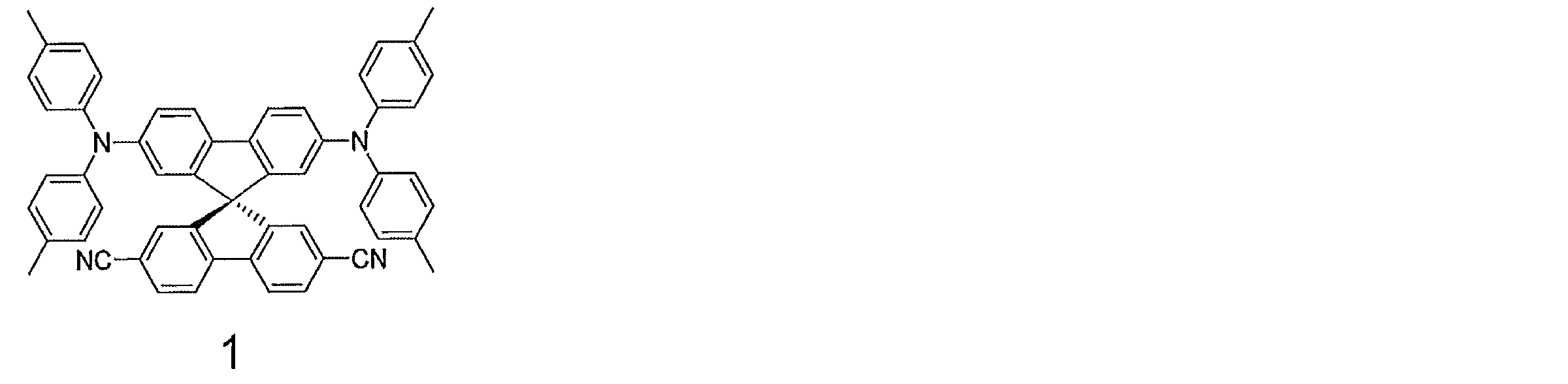
- the compound 4 having two 9-carbazolyl groups is a known compound and can be synthesized by combining known compound synthesis methods.
- Compound 1 can be converted to 2 ′, 7′-diiodinated-2,7-dicyanospirobifluorene by diiodating 2,7-dicyanospirobifluorene with an iodinating agent and further reacted with diphenylamine.
- the compound of the present invention can also be synthesized by dibromating substituted spirobifluorene and reacting with a boronic acid having a structure of D1 to D10, for example.
- Other compounds of the present invention can also be synthesized by modifying these methods as necessary or combining them with known synthesis methods.
- the reaction conditions for each step can be selected from known reaction conditions.
- the organic electroluminescence device of the present invention has a structure having an anode, a cathode, and an organic layer between the anode and the cathode.
- the organic layer includes at least a light emitting layer, and may consist of only the light emitting layer, or may have one or more organic layers in addition to the light emitting layer.
- the organic electroluminescent element of this invention contains the compound represented by General formula (1) in a light emitting layer. If the compound represented by the general formula (1) is used as a thermally activated delayed fluorescent material in a light emitting layer of an organic electroluminescence device, high luminous efficiency can be achieved at a lower cost than before.
- the organic electroluminescence device of the present invention has extremely high current efficiency, power efficiency, and luminance, reaching the world's highest level at the present time, and is extremely useful.
- the organic electroluminescence element of the present invention has a structure in which at least an anode, an organic layer, and a cathode are laminated.
- the organic electroluminescence device of the present invention preferably comprises a plurality of organic layers.
- the organic layers other than the light-emitting layer are called a hole injection layer, a hole transport layer, an electron block layer, a light-emitting layer, a hole block layer, an electron transport layer, an electron injection layer, or the like depending on their functions. They can be used in combination.
- anode and cathode include: anode / light emitting layer / cathode, anode / hole injection layer / light emitting layer / cathode, anode / hole injection layer / hole transport layer / light emitting layer / cathode, anode / hole injection.
- anode / organic layer / cathode structures can be formed on a substrate.
- adopted by this invention is not limited to these.
- the compound represented by the general formula (1) is particularly preferably used for the light emitting layer, but the use of the compound represented by the general formula (1) as an organic material other than the light emitting layer as a charge transport material or the like is excluded. Not what you want.
- each organic layer or electrode constituting the organic electroluminescence element of the present invention When manufacturing each organic layer or electrode constituting the organic electroluminescence element of the present invention, a known manufacturing method can be appropriately selected and employed. For each organic layer or electrode, various materials employed in known organic electroluminescence elements can be selected and used. Furthermore, the organic electroluminescence element of the present invention can be modified as necessary with various modifications that can be easily conceived from known techniques and known techniques. Hereinafter, typical materials constituting the organic electroluminescence element will be described. However, materials that can be used for the organic electroluminescence element of the present invention are not limitedly interpreted by the following description.
- the substrate functions as a support for supporting the structure of the anode / organic layer / cathode and also functions as a substrate in manufacturing the structure of the anode / organic layer / cathode.
- the substrate may be made of a transparent material, or may be made of a translucent or opaque material. In the case where light emission is extracted from the anode side, it is preferable to use a transparent substrate. Examples of the material constituting the substrate include glass, quartz, metal, polycarbonate, polyester, polymethacrylate, and polysulfone. If a flexible substrate is used, a flexible organic electroluminescence element can be obtained.
- the anode has a function of injecting holes toward the organic layer.
- a material having a high work function is preferably used.
- a material having 4 eV or more is preferably used.
- metal for example, aluminum, gold, silver, nickel, palladium, platinum
- metal oxide for example, indium oxide, tin oxide, zinc oxide, a mixture of indium oxide and tin oxide [ITO], zinc oxide
- ITO indium oxide
- IZO metal halide
- carbon black carbon black.
- conductive polymers such as polyaniline, poly (3-methylthiophene), polypyrrole and the like.
- the transmittance is preferably 10% or more, more preferably 50% or more, and further preferably 80% or more.
- the thickness of the anode is usually 3 nm or more and preferably 10 nm or more.
- the upper limit can be set to, for example, 1 ⁇ m or less, but may be thicker when transparency is not required for the anode.
- the anode may have the above function as a substrate.
- the anode can be formed, for example, by vapor deposition, sputtering, or coating.
- a conductive polymer When a conductive polymer is used for the anode, it is also possible to form the anode on the substrate using an electrolytic polymerization method.
- surface treatment can be performed for the purpose of improving the hole injection function. Specific examples of the surface treatment include plasma treatment (for example, argon plasma treatment, oxygen plasma treatment), UV treatment, ozone treatment, and the like.
- the hole injection layer has a function of transporting holes from the anode to the light emitting layer side. Since the hole injection layer is generally formed on the anode, the hole injection layer is preferably a layer having excellent adhesion to the anode surface. For this reason, it is preferable to be comprised with the material with high thin film formation ability.
- the hole transport layer has a function of transporting holes to the light emitting layer side.
- the hole transport layer is made of a material excellent in hole transportability.
- a hole transport material having high hole mobility and low ionization energy is used. An ionization energy of, for example, 4.5 to 6.0 eV can be preferably selected.
- As the hole transport material various materials that can be used for the hole injection layer or the hole transport layer of the organic electroluminescence element can be appropriately selected and used.
- the hole transport material may be a polymer material having a repeating unit or a low molecular compound.
- hole transport materials include aromatic tertiary amine compounds, styrylamine compounds, oxadiazole derivatives, imidazole derivatives, triazole derivatives, pyrazoline derivatives, pyrazolone derivatives, phenylenediamine derivatives, arylamine derivatives, amino-substituted chalcone derivatives, oxazoles
- Examples thereof include derivatives, polyarylalkane derivatives, styrylanthracene derivatives, fluorenone derivatives, hydrazone derivatives, stilbene derivatives, silazane derivatives, silane polymers, aniline copolymers, thiophene polymers, and porphyrin compounds.
- Preferred examples of the hole transporting material include aromatic tertiary amine compounds. Specifically, triphenylamine, tolylamine, N, N′-diphenyl-N, N ′-(3-methylphenyl) -1 , 1′-biphenyl-4,4′-diamine, N, N, N ′, N ′-(4-methylphenyl) -1,1′-phenyl-4,4′-diamine, N, N, N ′ , N ′-(4-Methylphenyl) -1,1′-biphenyl-4,4′-diamine, N, N′-diphenyl-N, N′-dinaphthyl-1,1′-biphenyl-4,4 ′ -Diamine, N, N '-(methylphenyl) -N, N'-(4-n-butylphenyl) -phenanthrene-9,10-diamine, N, N-bis (4
- phthalocyanine compounds can also be mentioned as preferable hole transport materials, and specifically, H 2 Pc, CuPc, CoPc, NiPc, ZnPc, PdPc, FePc, MnPc, ClAlPc, ClGaPc, ClInPc, ClSnPc, Cl 2 SiPc , (HO) AlPc, (HO) GaPc, VOPc, TiOPc, MoOPc, and GaPc—O—GaPc [Pc represents phthalocyanine].
- metal oxides such as poly (ethylenedioxy) thiophene (PEDOT) and molybdenum oxide, and known aniline derivatives can also be preferably used.
- the hole transport material used in the present invention may be used by selecting only one kind per layer, or may be used by combining two or more kinds per layer.
- the hole injection layer and the hole transport layer can be formed by, for example, a vapor deposition method, a sputtering method, or a coating method.
- the thickness of the hole injection layer or the hole transport layer is usually 3 nm or more, and preferably 10 nm or more.
- the upper limit value can be set to 5 ⁇ m or less, for example.
- the light emitting layer of the organic electroluminescence device of the present invention may contain a host material and a dopant material, or may consist of only a single material.
- the light emitting layer of the organic electroluminescent element of the present invention contains a compound represented by the general formula (1).
- the dopant material is preferably used at 10 wt% or less, more preferably 6 wt% or less, in order to prevent concentration quenching.
- the dopant material and the host material one kind of material may be used alone, or two or more kinds of materials may be used in combination. Doping can be performed by co-evaporation of a host material and a dopant material. At this time, the host material and the dopant material may be mixed in advance and then simultaneously deposited.
- Examples of the host material used for the light-emitting layer include carbazole derivatives, quinolinol derivative metal complexes, oxadiazole derivatives, distyrylarylene derivatives, and diphenylanthracene derivatives.
- materials proposed as host materials for the light emitting layer can be appropriately selected and used.
- a preferred host material for example, a compound represented by the following general formula (10) can be given.
- Z represents a q-valent linking group, and q represents an integer of 2 to 4.
- R 101 and R 102 each independently represent a substituent, and n 101 and n 102 each independently represent an integer of 0 to 4.
- n101 is any integer of 2 to 4
- n101 R 101's may be the same as or different from each other
- n102 R 102 may be the same as or different from each other.
- R 101 , R 102 , n101 and n102 in each of q structural units may be the same as or different from each other.
- Examples of the substituent represented by R 101 and R 102 in the general formula (10) include a substituted or unsubstituted alkyl group, a substituted or unsubstituted alkoxy group, a substituted or unsubstituted aryl group, and a substituted or unsubstituted aryloxy group. And a substituted or unsubstituted alkenyl group, a substituted or unsubstituted amino group, a halogen atom, and a cyano group.
- n101 and n102 are each independently preferably an integer of 0 to 3, more preferably an integer of 0 to 2. Moreover, it is also preferable that both n101 and n102 are 0.
- Z in the general formula (10) is preferably a linking group containing an aromatic ring or a heterocyclic ring.
- the aromatic ring may be a single ring or a fused ring in which two or more aromatic rings are fused.
- the number of carbon atoms in the aromatic ring is preferably 6 to 22, more preferably 6 to 18, still more preferably 6 to 14, and still more preferably 6 to 10.
- Specific examples of the aromatic ring include a benzene ring and a naphthalene ring.
- the heterocyclic ring may be a single ring or a fused ring in which one or more heterocyclic rings and an aromatic ring or a heterocyclic ring are fused.
- the number of carbon atoms in the heterocyclic ring is preferably 5 to 22, more preferably 5 to 18, still more preferably 5 to 14, and still more preferably 5 to 10.
- the hetero atom constituting the heterocyclic ring is preferably a nitrogen atom.
- Specific examples of the heterocyclic ring include a pyridine ring, a pyridazine ring, a pyrimidine ring, a triazine ring, a triazole ring, and a benzotriazole ring.
- Z in the general formula (10) contains an aromatic ring or a heterocyclic ring, and may contain a non-aromatic linking group. Examples of such a non-aromatic linking group include those having the following structure.
- R 107 , R 108 , R 109 and R 110 in the above non-aromatic linking group each independently represents a hydrogen atom, a substituted or unsubstituted alkyl group, or a substituted or unsubstituted aryl group, substituted or unsubstituted It is preferable that the alkyl group is a substituted or unsubstituted aryl group.
- R 111 , R 112 and R 113 each independently represent a substituent, n111 and n112 each independently represent an integer of 1 to 4, and n113 is any of 1 to 5 Represents an integer.
- At least one R 111 , at least one R 112 , and at least one R 113 are aryl groups.
- n111 is an integer of 2 to 4, it may be the being the same or different each n111 amino R 111
- n112 is an integer of 2 to 4
- n112 amino R 112 may be the same as or different from each other.
- n113 is an integer of 2 to 5
- n113 R 113 may be the same as or different from each other.
- n111, n112 and n113 are preferably 1 to 3, more preferably 1 or 2.
- the hole blocking layer has a function of preventing holes passing through the light emitting layer from moving to the cathode side. It is preferably formed between the light emitting layer and the organic layer on the cathode side.
- the organic material forming the hole blocking layer include an aluminum complex compound, a gallium complex compound, a phenanthroline derivative, a silole derivative, a quinolinol derivative metal complex, an oxadiazole derivative, and an oxazole derivative.
- BCP 2,9-dimethyl And -4,7-diphenyl-1,10-phenanthroline
- the hole block layer can be formed by, for example, a vapor deposition method, a sputtering method, or a coating method.
- the thickness of the hole block layer is usually 3 nm or more, and preferably 10 nm or more.
- the upper limit value can be set to 5 ⁇ m or less, for example.
- the electron injection layer has a function of transporting electrons from the cathode to the light emitting layer. Since the electron injection layer is generally formed so as to be in contact with the cathode, it is preferably a layer having excellent adhesion to the cathode surface.
- the electron transport layer has a function of transporting electrons to the light emitting layer side.
- the electron transport layer is made of a material having excellent electron transport properties. For the electron injection layer and the electron transport layer, an electron transport material having high electron mobility and high ionization energy is used. As the electron transport material, various materials that can be used for the electron injection layer or the electron transport layer of the organic electroluminescence element can be appropriately selected and used.
- the electron transport material may be a polymer material having a repeating unit or a low molecular compound.
- electron transport materials include fluorenone derivatives, anthraquinodimethane derivatives, diphenoquinone derivatives, thiopyran dioxide derivatives, oxazole derivatives, thiazole derivatives, oxadiazole derivatives, triazole derivatives, imidazole derivatives, perylenetetracarboxylic acid derivatives, quinoxaline derivatives. , Fluorenylidenemethane derivatives, anthraquinodimethane derivatives, anthrone derivatives and the like.
- preferred electron transport materials include 2,5-bis (1-phenyl) -1,3,4-oxazole, 2,5-bis (1-phenyl) -1,3,4-thiazole, 2,5 -Bis (1-phenyl) -1,3,4-oxadiazole, 2- (4′-tert-butylphenyl) -5- (4 ′′ -biphenyl) 1,3,4-oxadiazole, 2, 5-bis (1-naphthyl) -1,3,4-oxadiazole, 1,4-bis [2- (5-phenyloxadiazolyl)] benzene, 1,4-bis [2- (5-phenyl) Oxadiazolyl) -4-tert-butylbenzene], 2- (4′-tert-butylphenyl) -5- (4 ′′ -biphenyl) -1,3,4-thiadiazole, 2,5-bis (1- Naphthyl) -1,3,4-thiadiazole, 1,4-
- the electron transport material used in the present invention may be used by selecting only one kind for one layer, or may be used by combining two or more kinds for one layer.
- the electron injection layer and the electron transport layer can be formed by, for example, a vapor deposition method, a sputtering method, or a coating method.
- the thickness of the electron injection layer or the electron transport layer is usually 3 nm or more, and preferably 10 nm or more.
- the upper limit value can be set to 5 ⁇ m or less, for example.
- the cathode has a function of injecting electrons toward the organic layer.
- a material having a low work function is preferably used.
- a material having 4 eV or less is preferably used.
- Specific examples include metals (eg, tin, magnesium, indium, calcium, aluminum, silver) and alloys (eg, aluminum-lithium alloy, magnesium-silver alloy, magnesium-indium alloy).
- metals eg, tin, magnesium, indium, calcium, aluminum, silver
- alloys eg, aluminum-lithium alloy, magnesium-silver alloy, magnesium-indium alloy.
- the transmittance is preferably 10% or more, more preferably 50% or more, and further preferably 80% or more.
- the thickness of the cathode is usually 3 nm or more, and preferably 10 nm or more.
- the upper limit value can be set to 1 ⁇ m or less, for example, but may be thicker if the cathode is not required to be transparent.
- the cathode can be formed, for example, by vapor deposition or sputtering.
- a protective layer is preferably formed on the cathode in order to protect the cathode.
- Such a protective layer is preferably a layer made of a stable metal having a high work function. For example, a metal layer such as aluminum, silver, copper, nickel, chromium, gold, or platinum can be formed.
- the organic electroluminescence device of the present invention can be further applied to various uses. For example, it is possible to produce an organic electroluminescence display device using the organic electroluminescence element of the present invention. For details, see “Organic EL Display” by Osamu Shigeru Tokito, Chiba Adachi, and Hideyuki Murata. ) Can be referred to. In particular, the organic electroluminescence device of the present invention can be applied to organic electroluminescence illumination that is in great demand.
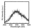
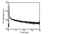
- Example 1 In this example, a test was conducted using Compound 1, and an organic electroluminescence device having the structure shown in FIG. 1 was produced. (1) Observation of delayed fluorescence 6% by weight of Compound 1 and mCP were co-evaporated to form a film on a quartz substrate, and an emission spectrum was measured (FIG. 2). The co-deposited film showed yellow light emission, and the PL quantum yield was as high as 27%. Next, in order to examine the thermally activated delayed fluorescence characteristics of Compound 1, the PL transient attenuation of the co-deposited film was measured at 300 K using a streak camera (FIG. 3).
- the PL transient decay curve was in good agreement with the two-component fitting, and a 24 ns short-life component and a 24 ⁇ s long-life component were observed. That is, with compound 1, in addition to short-lived fluorescence, thermally activated delayed fluorescence derived from long-lived components was observed.
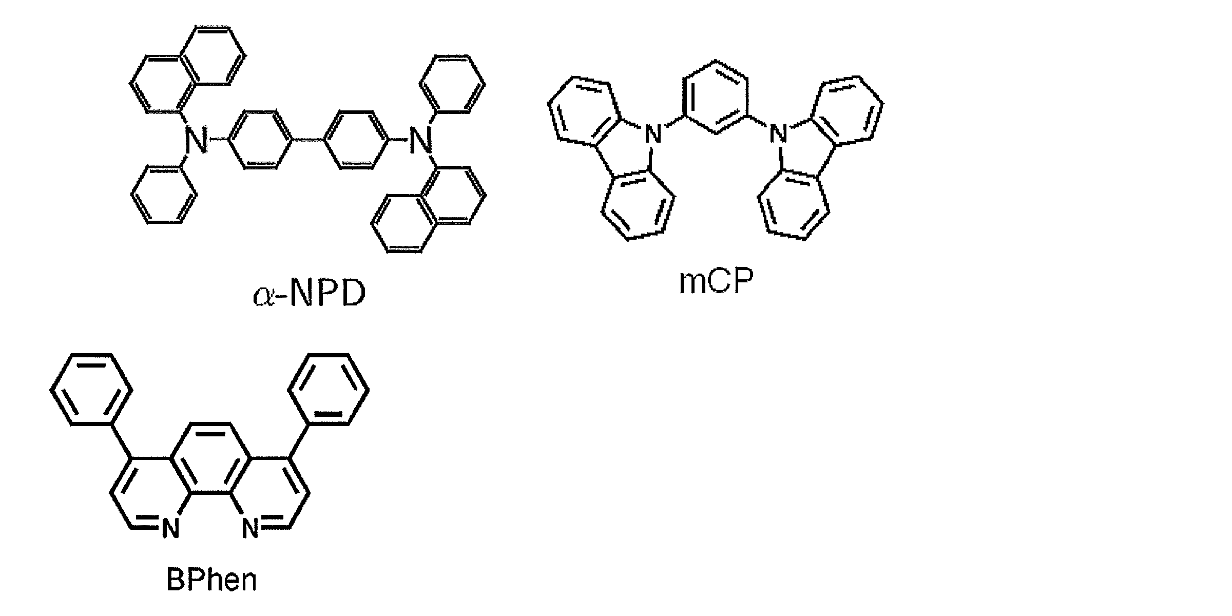
- ITO 2 Indium tin oxide (ITO) 2 is formed on glass 1 with a thickness of about 30 to 100 nm, and further, N, N′-di (naphthalene-1- Yl) -N, N′-diphenylbenzidine ( ⁇ -NPD) 3 was formed to a thickness of 60 nm. Then, 6% by weight of Compound 1 and 4,4-bis [N- (1-naphthyl) -N-phenylamino)] biphenyl (mCP) are co-evaporated to form a light emitting layer 4 with a thickness of 20 nm. did.
- Bphen 4,7-diphenyl-1,10-phenanthrolin (Bphen) 5 was formed to a thickness of 40 nm.
- magnesium-silver (MgAg) 6 was vacuum-deposited with a thickness of 100 nm, and then silver (Ag) 7 was vapor-deposited with a thickness of 20 nm to obtain an organic electroluminescence device having the layer structure shown in FIG.
- the result of having measured the emission spectrum of the manufactured organic electroluminescent element is shown in FIG. Yellow light emission was observed at the maximum current.
- the graph shown in FIG. 5 was obtained. In FIG.
- FIG. 6 is a graph showing the relationship between the reciprocal of temperature and the intensity ratio of long-life luminescence to single-life luminescence (Berberan-Santos Plot). The energy difference ( ⁇ E ST ) between the T1 level and the S1 level was 0.057 eV, which was confirmed to be extremely small as compared with the conventional delayed fluorescent material.
- FIG. 8 is a graph showing the relationship between current density and external quantum efficiency.
- FIG. 9 is a graph showing the results of measuring current density-voltage-luminance (JVL) characteristics using a semiconductor parameter-analyzer and a power meter. 12000 cd / m 2 was achieved at a current efficiency of 13.5 cd / A, a power efficiency of 13.0 lm / W, and a drive voltage of 15V.
- JVL current density-voltage-luminance
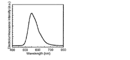
- Example 42 In this example, a toluene solution of compound 4 was prepared and the emission spectrum was measured (FIG. 9). When PL transient attenuation was measured in the same manner as in Example 1, a short-life component of 11.55 ns and a long-life component of 124.9 ⁇ s were observed (FIG. 10). That is, by the compound 4, in addition to the short-lived fluorescence, thermally activated delayed fluorescence derived from the long-lived component was observed.
- Example 43 Using the compound 10 synthesized in Synthesis Example 1, the emission spectrum of the solution was measured in the same manner as in Example 42. As a result, light emission having a peak at 550 nm was observed. Further, when PL transient attenuation was measured, a short-life component of 10.61 ns and a long-life component of 434.38 ⁇ s were observed (FIG. 11). That is, by the compound 10, in addition to the short-lived fluorescence, thermally activated delayed fluorescence derived from the long-lived component was observed.
- the organic electroluminescence element of the present invention can be manufactured at low cost, and can achieve high luminance with high luminous efficiency.
- the delayed fluorescent material of the present invention is useful as a light emitting material for such an organic electroluminescence device. For this reason, this invention has high industrial applicability.
Landscapes
- Chemical & Material Sciences (AREA)
- Organic Chemistry (AREA)
- Engineering & Computer Science (AREA)
- Materials Engineering (AREA)
- Physics & Mathematics (AREA)
- Optics & Photonics (AREA)
- Spectroscopy & Molecular Physics (AREA)
- Electroluminescent Light Sources (AREA)
- Organic Low-Molecular-Weight Compounds And Preparation Thereof (AREA)
Abstract
Description

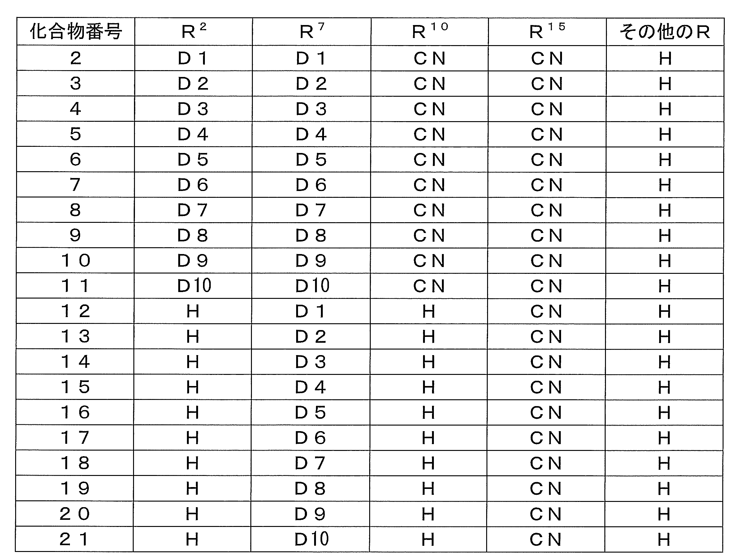
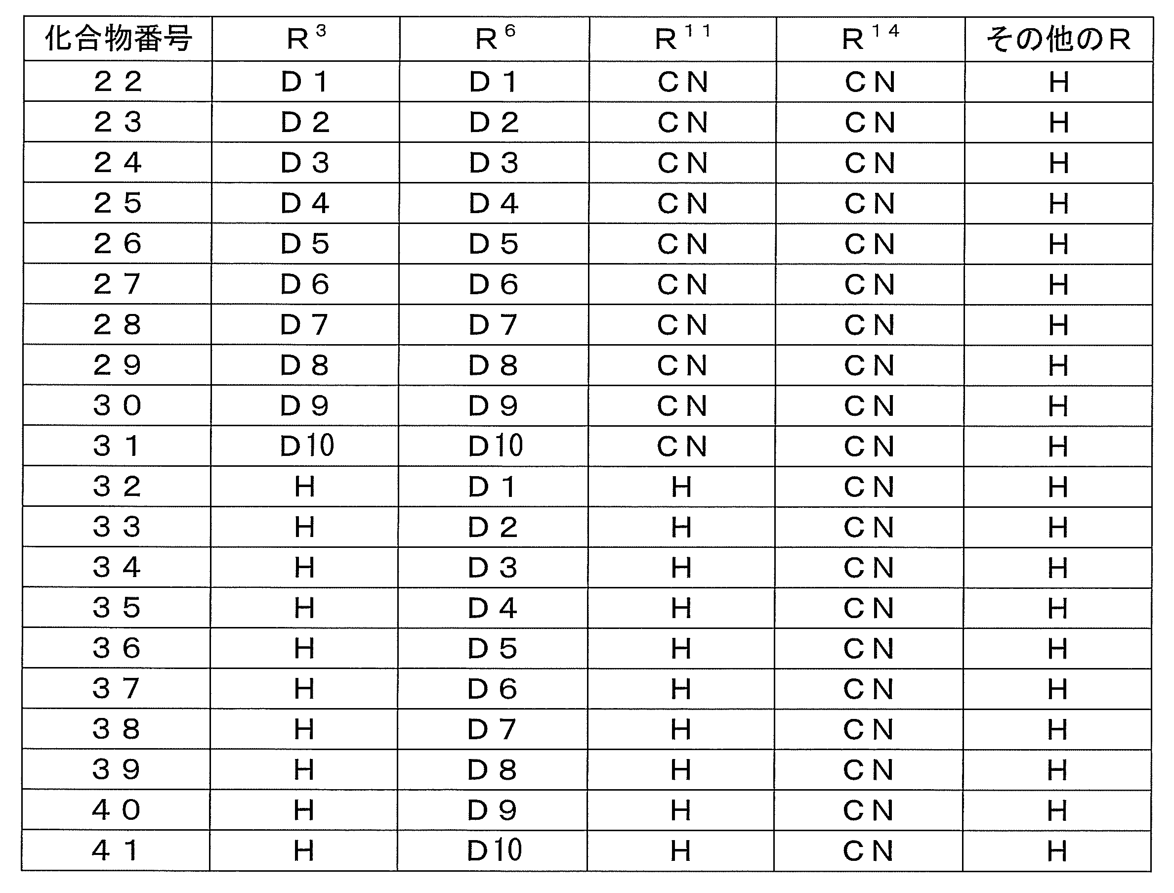
[2] 一般式(1)のR1、R2、R3、R4、R5、R6、R7およびR8の少なくとも2つが電子供与基であることを特徴とする[1]に記載の遅延蛍光材料。
[3] 一般式(1)のR1、R2、R3およびR4の少なくとも1つが電子供与基であって、R5、R6、R7およびR8の少なくとも1つが電子供与基であることを特徴とする[1]に記載の遅延蛍光材料。
[4] 一般式(1)のR2およびR3の少なくとも1つが電子供与基であって、R6およびR7の少なくとも1つが電子供与基であることを特徴とする[1]に記載の遅延蛍光材料。
[5] 一般式(1)のR2またはR3が電子供与基であって、R6またはR7が電子供与基であることを特徴とする[1]に記載の遅延蛍光材料。
[6] R1、R2、R3、R4、R5、R6、R7およびR8の少なくとも1つは、下記一般式(2)~(4)のいずれかで表される骨格を含む電子供与基であることを特徴とする[1]~[5]のいずれか一項に記載の遅延蛍光材料。
[7] R1、R2、R3、R4、R5、R6、R7およびR8の少なくとも1つは、下記D1~D10のいずれかの骨格を含む電子供与基であることを特徴とする[1]~[5]のいずれか一項に記載の遅延蛍光材料。

[9] 一般式(1)のR9、R10、R11、R12、R13、R14、R15およびR16の少なくとも2つが電子吸引基であることを特徴とする[1]~[8]のいずれか一項に記載の遅延蛍光材料。
[10] 一般式(1)のR9、R10、R11およびR12の少なくとも1つが電子吸引基であって、R13、R14、R15およびR16の少なくとも1つが電子吸引基であることを特徴とする[1]~[8]のいずれか一項に記載の遅延蛍光材料。
[11] 一般式(1)のR10またはR11が電子吸引基であって、R14またはR15が電子吸引基であることを特徴とする[1]~[8]のいずれか一項に記載の遅延蛍光材料。
[12] 一般式(1)のR10またはR11がシアノ基であって、R14またはR15がシアノ基であることを特徴とする[1]~[8]のいずれか一項に記載の遅延蛍光材料。
[14] 下記一般式(1’)で表される化合物。

[15] R1、R2、R3、R4、R5、R6、R7およびR8の少なくとも1つは上記D1~D8のいずれかで表される骨格を含む電子供与基であることを特徴とする[14]に記載の化合物。
[16] R1、R2、R3、R4、R5、R6、R7およびR8の少なくとも1つが前記D9で表される骨格を含む電子供与基であることを特徴とする[15]に記載の化合物。
本発明の遅延蛍光材料は、下記一般式(1)で表される化合物からなることを特徴とする。そこで、一般式(1)で表される化合物について、まず説明する。
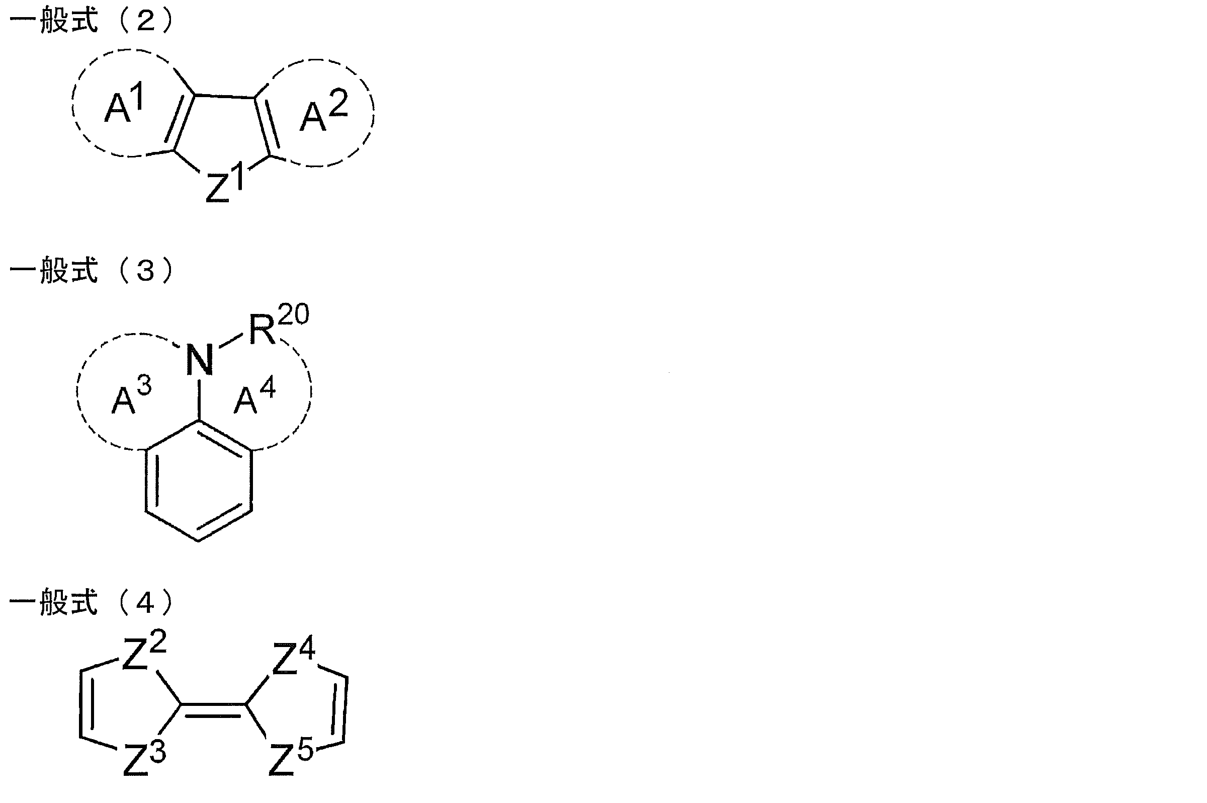
一般式(2)のA1およびA2が環構造を形成しているとき、その環構造は複数の環が融合した融合環構造であってもい。そのような融合環は、芳香環どうしが融合したものであってもよいし、ヘテロ芳香環どうしが融合したものであってもよいし、脂肪環どおりが融合したものであってもよいし、さらには芳香環とヘテロ芳香環のように異なる種類の環が融合したものであってもよく、特に制限されない。また、融合する環どうしは同一であっても異なっていてもよい。例えば、Z1が硫黄原子であるとき、A1がフラン環がベンゼン環に融合した環構造を形成していて、A2が環構造を形成していない場合は、一般式(2)はベンゾジフラン骨格を表す。
一般式(2)のA1およびA2が形成しうる環構造は、芳香環または複素芳香環であることが好ましく、芳香環であることがより好ましい。

本明細書でいうアルキル基は、直鎖状であっても、分枝状であっても、環状であってもよい。好ましいのは直鎖状または分枝状のアルキル基である。アルキル基の炭素数は、1~20であることが好ましく、1~12であることがより好ましく、1~6であることがさらに好ましく、1~3であること(すなわちメチル基、エチル基、n-プロピル基、イソプロピル基)がさらにより好ましい。環状のアルキル基としては、例えばシクロペンチル基、シクロヘキシル基、シクロヘプチル基を挙げることができる。
本明細書でいうアリール基は、1つの芳香環からなるものであってもよいし、2以上の芳香環が融合した構造を有するものであってもよい。アリール基の環構成炭素数は、6~22であることが好ましく、6~18であることがより好ましく、6~14であることがさらに好ましく、6~10であること(すなわちフェニル基、1-ナフチル基、2-ナフチル基)がさらにより好ましく、フェニル基が最も好ましい。
本明細書でいうアルコキシ基は、直鎖状であっても、分枝状であっても、環状であってもよい。好ましいのは直鎖状または分枝状のアルコキシ基である。アルコキシ基の炭素数は、1~20であることが好ましく、1~12であることがより好ましく、1~6であることがさらに好ましく、1~3であること(すなわちメトキシ基、エトキシ基、n-プロポキシ基、イソプロポキシ基)がさらにより好ましい。環状のアルコキシ基としては、例えばシクロペンチルオキシ基、シクロヘキシルオキシ基、シクロヘプチルオキシ基を挙げることができる。
本明細書でいうアリールオキシ基は、1つの芳香環からなるものであってもよいし、2以上の芳香環が融合した構造を有するものであってもよい。アリールオキシ基の炭素数は、6~22であることが好ましく、6~18であることがより好ましく、6~14であることがさらに好ましく、6~10であること(すなわちフェニルオキシ基、1-ナフチルオキシ基、2-ナフチルオキシ基)がさらにより好ましい。
一般式(1)で表される化合物の別の集合体として、例えば、R1、R2、R3、R4、R5、R6、R7、R8、R9、R10、R11、R12、R13、R14、R15およびR16のうちの11~14個が水素原子である化合物群を挙げることもできる。このとき、R1、R2、R3、R4、R5、R6、R7およびR8のうちの4~7個が水素原子であることが好ましく、6または7個が水素原子であることがより好ましい。また、R9、R10、R11、R12、R13、R14、R15およびR16のうちの4~7個が水素原子であることが好ましく、6または7個が水素原子であることがより好ましい。好ましい例として、R1、R2、R3、R4、R5、R6、R7およびR8のうちの7個が水素原子であって、なおかつR9、R10、R11、R12、R13、R14、R15およびR16のうちの7個が水素原子である化合物や、R1、R2、R3、R4、R5、R6、R7およびR8のうちの6個が水素原子であって、なおかつR9、R10、R11、R12、R13、R14、R15およびR16のうちの6個が水素原子である化合物を挙げることができる。
一般式(1)で表される化合物のさらに別の集合体として、例えば、モノスピロビフルオレン化合物群を挙げることもできる。この化合物群では、R1、R2、R3、R4、R5、R6、R7、R8、R9、R10、R11、R12、R13、R14、R15およびR16が、スピロビフルオレン環を含む基であることはない。

本発明の有機エレクトロルミネッセンス素子は、陽極、陰極、および陽極と陰極の間に有機層を有する構造を備えている。有機層は、少なくとも発光層を含むものであり、発光層のみからなるものであってもよいし、発光層の他に1層以上の有機層を有するものであってもよい。本発明の有機エレクトロルミネッセンス素子は、発光層に一般式(1)で表される化合物を含むものである。
一般式(1)で表される化合物を、熱活性化遅延蛍光材料として有機エレクトロルミネッセンス素子の発光層に用いれば、高い発光効率を従来よりも安価に達成しうる。従来は、発光効率が高い有機エレクトロルミネッセンス素子を製造するために、励起子生成効率が高いリン光材料を用いた研究が活発に行われてきた。しかしながら、リン光材料を用いる場合は、IrやPtといった希少金属を利用する必要があるため、コストが高くなるという問題があった。遅延蛍光材料を用いれば、このような高価な材料を必要としないため、発光効率が高い有機エレクトロルミネッセンス素子を安価に提供することが可能になる。特に一般式(1)で表される化合物は、T1レベルとS1レベルのエネルギー差(ΔEST)が従来の遅延蛍光材料と比べて極めて小さい。そして、一般式(1)で表される化合物を用いた有機エレクトロルミネッセンス素子によれば、従来は低かった外部量子効率を飛躍的に高めることができる。本発明の有機エレクトロルミネッセンス素子は、電流効率、電力効率、輝度のいずれも極めて高く、現時点における世界最高水準に達するものであり、極めて有用である。
基板は、陽極\有機層\陰極の構造を支える支持体として機能するとともに、陽極\有機層\陰極の構造を製造する際の基板として機能するものである。基板は、透明材料で構成されていても、半透明ないし不透明な材料で構成されていてもよい。陽極側から発光を取り出す場合は、透明な基板を用いることが好ましい。基板を構成する材料として、ガラス、石英、金属、ポリカーボネート、ポリエステル、ポリメタクリレート、ポリスルホンを挙げることができる。可撓性を有する基板を用いれば、フレキシブルな有機エレクトロルミネッセンス素子とすることができる。
陽極は、有機層へ向けてホールを注入する機能を有する。そのような陽極としては、仕事関数が高い材料を用いることが好ましく、例えば4eV以上の材料を用いることが好ましい。具体的には、金属(例えば、アルミニウム、金、銀、ニッケル、パラジウム、白金)、金属酸化物(例えば、酸化インジウム、酸化スズ、酸化亜鉛、酸化インジウムと酸化スズの混合物[ITO]、酸化亜鉛と酸化インジウムの混合物[IZO])、ハロゲン化金属(例えば、ヨウ化銅)、カーボンブラックを挙げることができる。また、ポリアニリン、ポリ(3-メチルチオフェン)、ポリピロール等の導電性ポリマーを用いることも可能である。陽極側から発光を取り出す場合は、ITOやIZOなどの発光に対する透過率が高い材料を用いることが好ましい。透過率は、10%以上であることが好ましく、50%以上であることがより好ましく、80%以上であることがさらに好ましい。また、陽極の厚みは、通常は3nm以上であり、10nm以上であることが好ましい。上限値は、例えば1μm以下とすることができるが、陽極に透明性が要求されない場合はさらに厚くてもよく、例えば、上記の基板としての機能を陽極が兼ね備えるようにすることもできる。陽極は、例えば蒸着法、スパッタリング法、塗布法により形成することができる。導電性ポリマーを陽極に用いる場合は、電解重合法を用いて基板上に陽極を形成することも可能である。陽極の形成後は、ホール注入機能を向上させること等を目的として表面処理を行うことができる。表面処理の具体例として、プラズマ処理(例えば、アルゴンプラズマ処理、酸素プラズマ処理)、UV処理、オゾン処理などが挙げられる。
ホール注入層は、ホールを陽極から発光層側へ輸送する機能を有する。ホール注入層は、一般に陽極の上に形成されることから、陽極表面との密着性に優れた層であることが好ましい。このため、薄膜形成能が高い材料で構成されることが好ましい。ホール輸送層は、ホールを発光層側へ輸送する機能を有している。ホール輸送層には、ホール輸送性に優れた材料から構成される。
ホール注入層およびホール輸送層には、ホール移動度が高くてイオン化エネルギーが小さいホール輸送材料を用いる。イオン化エネルギーは、例えば4.5~6.0eVのものを好ましく選択することができる。ホール輸送材料としては、有機エレクトロルミネッセンス素子のホール注入層またはホール輸送層に用いることができるとされている種々の材料を適宜選択して用いることができる。ホール輸送材料は、繰り返し単位を有するポリマー材料であってもよいし、低分子化合物であってもよい。
本発明の有機エレクトロルミネッセンス素子の発光層は、ホスト材料とドーパント材料を含むものであってもよいし、単一材料のみからなるものであってもよい。本発明の有機エレクトロルミネッセンス素子の発光層は、一般式(1)で表される化合物を含む。
発光層がホスト材料とドーパント材料を含むとき、濃度消光を防ぐために、ドーパント材料はホスト材料に対して10重量%以下で用いることが好ましく、6重量%以下で用いることがより好ましい。ドーパント材料およびホスト材料は、いずれも1種の材料を単独で用いてもよいし、2種以上の材料を組み合わせて用いてもよい。ドーピングは、ホスト材料とドーパント材料を共蒸着することにより行うことができるが、このときホスト材料とドーパント材料はあらかじめ混合しておいてから同時に蒸着してもよい。

n101およびn102は、各々独立に0~3のいずれかの整数であることが好ましく、0~2のいずれかの整数であることがより好ましい。また、n101およびn102がいずれも0であるものも好ましい。


一般式(11)におけるn111、n112およびn113は1~3であることが好ましく、1または2であることがより好ましい。

ホールブロック層は、発光層を経由したホールが陰極側へ移動するのを防げる機能を有する。発光層と陰極側の有機層との間に形成されることが好ましい。ホールブロック層を形成する有機材料としては、アルミニウム錯体化合物、ガリウム錯体化合物、フェナントロリン誘導体、シロール誘導体、キノリノール誘導体金属錯体、オキサジアゾール誘導体、オキサゾール誘導体を挙げることができる。具体的には、ビス(8-ヒドロキシキノリナート)(4-フェニルフェノラート)アルミニウム、ビス(2-メチル-8-ヒドロキシキノリナート)(4-フェニルフェノラート)ガリウム、2,9-ジメチル-4,7-ジフェニル-1,10-フェナントロリン(BCP)等を挙げることができる。ホールブロック層には、1種の有機材料を選択して単独で用いてもよいし、2種以上を組み合わせて用いてもよい。また、ホールブロック層は、例えば蒸着法、スパッタリング法、塗布法により形成することができる。ホールブロック層の厚みは、通常は3nm以上であり、10nm以上であることが好ましい。上限値は、例えば5μm以下とすることができる。
電子注入層は、電子を陰極から発光層側へ輸送する機能を有する。電子注入層は、一般に陰極に接するように形成されることから、陰極表面との密着性に優れた層であることが好ましい。電子輸送層は、電子を発光層側へ輸送する機能を有している。電子輸送層には、電子輸送性に優れた材料から構成される。
電子注入層および電子輸送層には、電子移動度が高くてイオン化エネルギーが大きい電子輸送材料を用いる。電子輸送材料としては、有機エレクトロルミネッセンス素子の電子注入層または電子輸送層に用いることができるとされている種々の材料を適宜選択して用いることができる。電子輸送材料は、繰り返し単位を有するポリマー材料であってもよいし、低分子化合物であってもよい。
陰極は、有機層へ向けて電子を注入する機能を有する。そのような陰極としては、仕事関数が低い材料を用いることが好ましく、例えば4eV以下の材料を用いることが好ましい。具体的には、金属(例えば、スズ、マグネシウム、インジウム、カルシウム、アルミニウム、銀)、合金(例えば、アルミニウム-リチウム合金、マグネシウム-銀合金、マグネシウム-インジウム合金)を挙げることができる。陰極側から発光を取り出す場合は、透過率が高い材料を用いることが好ましい。透過率は、10%以上であることが好ましく、50%以上であることがより好ましく、80%以上であることがさらに好ましい。また、陰極の厚みは、通常は3nm以上であり、10nm以上であることが好ましい。上限値は、例えば1μm以下とすることができるが、陰極に透明性が要求されない場合はさらに厚くてもよい。陰極は、例えば蒸着法、スパッタリング法により形成することができる。陰極の上には、陰極を保護するために保護層を形成することが好ましい。そのような保護層は、仕事関数が高くて安定な金属からなる層であることが好ましく、例えば、アルミニウム、銀、銅、ニッケル、クロム、金、白金等の金属層を形成することができる。
本合成例において、以下のスキームにしたがって化合物10を合成した。
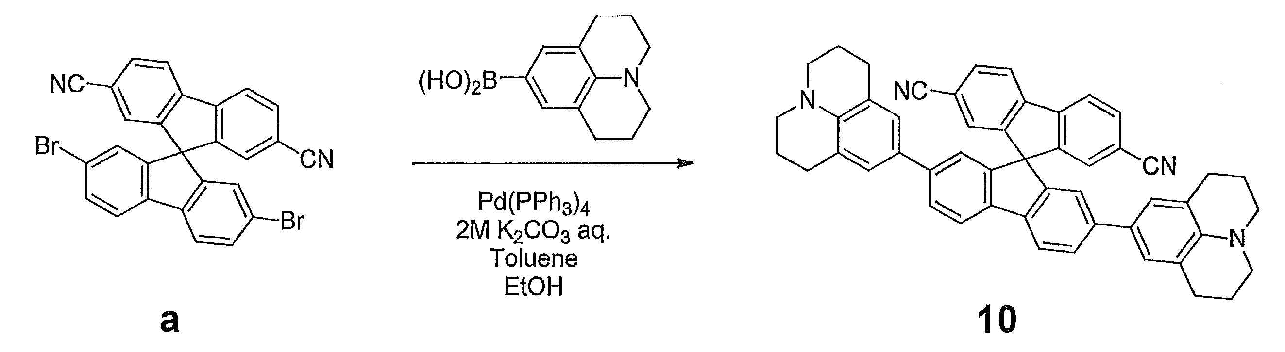
1H NMR (500MHz, CDCl3): 7.98 (d, J=8.0Hz, 2H), 7.83 (d, J=8.0Hz, 2H), 7.71 (d, J=8.0Hz, 2H), 7.57 (d, J=8.0Hz, 2H), 7.14 (s, 2H), 6.84 (s, 4H), 6.67 (s, 2H), 3.12 (d, J=11Hz, 8H), 2.72 (t, J=6.4Hz, 8H), 1.93 (d, J=11Hz, 8H).
MS(MALDI): m/z calcd: 708.33 [M+H]+; found: 708.29.
本実施例において、化合物1を用いて試験を行うとともに、図1に示す構造の有機エレクトロルミネッセンス素子を作製した。
(1)遅延蛍光の観測
6重量%の化合物1とmCPを共蒸着することにより石英基板上に製膜し、発光スペクトルを測定した(図2)。共蒸着膜は黄色発光を示し、PL量子収率は27%と高い値を示した。次に化合物1の熱活性化遅延蛍光特性を検討するために、ストリークカメラを用いて共蒸着膜のPL過渡減衰を300Kで測定した(図3)。PL過渡減衰曲線は2成分のフィッティングによく一致し、24nsの短寿命成分と24μsの長寿命成分が観測された。すなわち、化合物1によって、短寿命の蛍光に加え、長寿命成分に由来する熱活性化遅延蛍光が観測された。
ガラス1上にインジウム・スズ酸化物(ITO)2をおよそ30~100nmの厚さで製膜し、さらにその上にN,N’-ジ(ナフタレン-1-イル)-N,N’-ジフェニルベンジジン(α-NPD)3を60nmの厚さで製膜した。次いで、6重量%の化合物1と4,4-ビス[N-(1-ナフチル)-N-フェニルアミノ)]ビフェニル(mCP)を共蒸着することによって発光層4を20nmの厚さで製膜した。さらにその上に、4,7-ジフェニル-1,10-フェノアントロリン(Bphen)5を厚さ40nmで製膜した。次いで、マグネシウム-銀(MgAg)6を100nm真空蒸着し、次いで銀(Ag)7を20nmの厚さに蒸着して、図1に示す層構成を有する有機エレクトロルミネッセンス素子とした。
製造した有機エレクトロルミネッセンス素子の発光スペクトルを測定した結果を図4に示す。最大電流で黄色発光を示した。温度と発光効率の関係を測定したところ図5に示すグラフが得られた。図5において、ΦTOTALは全発光、ΦTADF長寿命発光(遅延蛍光)、ΦPromptは単寿命発光を示す。温度上昇に伴ってΦTADFが大きくなっていることが確認され、T1からS1へ効率良く変換されていることが示された。図6は、温度の逆数と長寿命発光の単寿命発光に対する強度比との関係を示すグラフである(Berberan-Santos Plot)。T1レベルとS1レベルのエネルギー差(ΔEST)は0.057eVであり、従来の遅延蛍光材料と比べて極めて小さいことが確認された。図8は、電流密度と外部量子効率の関係を示すグラフである。従来1.4%程度であった外部量子効率は、本実施例では4.4%に達した。図9は、半導体パラメータ-アナライザーおよびパワーメータを用いて電流密度-電圧-輝度(J-V-L)特性を測定した結果を示すグラフである。電流効率13.5cd/A、電力効率13.0 lm/W、駆動電圧15Vにおいて12000cd/m2を達成した。
実施例1と同様にして、化合物2~41についても有用性を確認することができる。
本実施例において、化合物4のトルエン溶液を調製して発光スペクトルを測定した(図9)。実施例1と同様にしてPL過渡減衰を測定したところ、11.55nsの短寿命成分と124.9μsの長寿命成分が観測された(図10)。すなわち、化合物4によって、短寿命の蛍光に加え、長寿命成分に由来する熱活性化遅延蛍光が観測された。

合成例1で合成した化合物10を用いて、実施例42と同様に溶液の発光スペクトルを測定したところ550nmをピークとする発光が認められた。また、PL過渡減衰を測定したところ、10.61nsの短寿命成分と434.38μsの長寿命成分が観測された(図11)。すなわち、化合物10によって、短寿命の蛍光に加え、長寿命成分に由来する熱活性化遅延蛍光が観測された。
2 ITO
3 mCP
4 発光層
5 Bphen
6 MgAg
7 Ag
Claims (16)
- 下記一般式(1)で表される化合物からなる遅延蛍光材料。

- 一般式(1)のR1、R2、R3、R4、R5、R6、R7およびR8の少なくとも2つが電子供与基であることを特徴とする請求項1に記載の遅延蛍光材料。
- 一般式(1)のR1、R2、R3およびR4の少なくとも1つが電子供与基であって、R5、R6、R7およびR8の少なくとも1つが電子供与基であることを特徴とする請求項1に記載の遅延蛍光材料。
- 一般式(1)のR2およびR3の少なくとも1つが電子供与基であって、R6およびR7の少なくとも1つが電子供与基であることを特徴とする請求項1に記載の遅延蛍光材料。
- 一般式(1)のR2またはR3が電子供与基であって、R6またはR7が電子供与基であることを特徴とする請求項1に記載の遅延蛍光材料。
- R1、R2、R3、R4、R5、R6、R7およびR8の少なくとも1つは、下記一般式(2)~(4)のいずれかで表される骨格を含む電子供与基であることを特徴とする請求項1~5のいずれか一項に記載の遅延蛍光材料。

- R1、R2、R3、R4、R5、R6、R7およびR8の少なくとも1つは、下記D1~D10のいずれかの骨格を含む電子供与基であることを特徴とする請求項1~5のいずれか一項に記載の遅延蛍光材料。
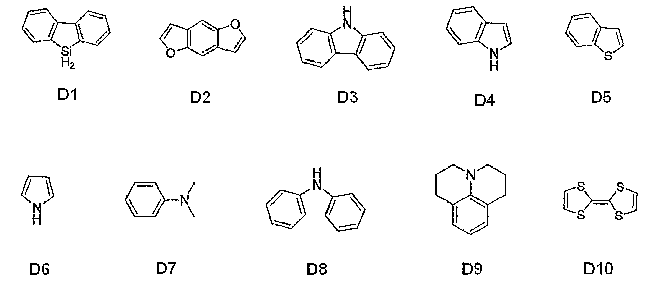
- R1、R2、R3、R4、R5、R6、R7およびR8の少なくとも1つが前記D3またはD9で表される骨格を含む電子供与基であることを特徴とする請求項7に記載の遅延蛍光材料。
- 一般式(1)のR9、R10、R11、R12、R13、R14、R15およびR16の少なくとも2つが電子吸引基であることを特徴とする請求項1~8のいずれか一項に記載の遅延蛍光材料。
- 一般式(1)のR9、R10、R11およびR12の少なくとも1つが電子吸引基であって、R13、R14、R15およびR16の少なくとも1つが電子吸引基であることを特徴とする請求項1~8のいずれか一項に記載の遅延蛍光材料。
- 一般式(1)のR10またはR11が電子吸引基であって、R14またはR15が電子吸引基であることを特徴とする請求項1~8のいずれか一項に記載の遅延蛍光材料。
- 一般式(1)のR10またはR11がシアノ基であって、R14またはR15がシアノ基であることを特徴とする請求項1~8のいずれか一項に記載の遅延蛍光材料。
- 陽極、陰極、および前記陽極と前記陰極の間に発光層を含む少なくとも1層の有機層を有する有機エレクトロルミネッセンス素子であって、請求項1~12のいずれか一項に記載の遅延蛍光材料を前記発光層に含むことを特徴とする有機エレクトロルミネッセンス素子。
- 下記一般式(1’)で表される化合物。


- R1、R2、R3、R4、R5、R6、R7およびR8の少なくとも1つは下記D1~D8のいずれかで表される骨格を含む電子供与基であることを特徴とする請求項14に記載の化合物。
- R1、R2、R3、R4、R5、R6、R7およびR8の少なくとも1つが前記D9で表される骨格を含む電子供与基であることを特徴とする請求項15に記載の化合物。
Priority Applications (5)
| Application Number | Priority Date | Filing Date | Title |
|---|---|---|---|
| CN201280035233.4A CN103688384B (zh) | 2011-07-15 | 2012-07-13 | 迟滞荧光材料及使用其的有机电致发光元件 |
| US14/233,012 US10454038B2 (en) | 2011-07-15 | 2012-07-13 | Delayed-fluorescence material and organic electroluminescence element using same |
| KR1020147003189A KR20140058550A (ko) | 2011-07-15 | 2012-07-13 | 지연 형광 재료 및 그것을 사용한 유기 일렉트로 루미네선스 소자 |
| JP2013524707A JP5875011B2 (ja) | 2011-07-15 | 2012-07-13 | 遅延蛍光材料およびそれを用いた有機エレクトロルミネッセンス素子 |
| EP12814370.8A EP2733761A4 (en) | 2011-07-15 | 2012-07-13 | MATERIAL WITH DELAYED FLUORESCENCE AND ORGANIC ELECTROLUMINESCENT ELEMENT THEREWITH |
Applications Claiming Priority (2)
| Application Number | Priority Date | Filing Date | Title |
|---|---|---|---|
| JP2011157032 | 2011-07-15 | ||
| JP2011-157032 | 2011-07-15 |
Publications (1)
| Publication Number | Publication Date |
|---|---|
| WO2013011955A1 true WO2013011955A1 (ja) | 2013-01-24 |
Family
ID=47558133
Family Applications (1)
| Application Number | Title | Priority Date | Filing Date |
|---|---|---|---|
| PCT/JP2012/067970 Ceased WO2013011955A1 (ja) | 2011-07-15 | 2012-07-13 | 遅延蛍光材料およびそれを用いた有機エレクトロルミネッセンス素子 |
Country Status (7)
| Country | Link |
|---|---|
| US (1) | US10454038B2 (ja) |
| EP (1) | EP2733761A4 (ja) |
| JP (1) | JP5875011B2 (ja) |
| KR (1) | KR20140058550A (ja) |
| CN (1) | CN103688384B (ja) |
| TW (1) | TW201309696A (ja) |
| WO (1) | WO2013011955A1 (ja) |
Cited By (40)
| Publication number | Priority date | Publication date | Assignee | Title |
|---|---|---|---|---|
| WO2014148493A1 (ja) * | 2013-03-18 | 2014-09-25 | 出光興産株式会社 | 発光装置 |
| WO2014157619A1 (ja) | 2013-03-29 | 2014-10-02 | 国立大学法人九州大学 | 有機エレクトロルミネッセンス素子 |
| JP2014532050A (ja) * | 2011-09-28 | 2014-12-04 | ソルヴェイ(ソシエテ アノニム) | 発光素子用のスピロビフルオレン化合物 |
| WO2015022974A1 (ja) | 2013-08-14 | 2015-02-19 | 国立大学法人九州大学 | 有機エレクトロルミネッセンス素子 |
| JP2015037138A (ja) * | 2013-08-14 | 2015-02-23 | コニカミノルタ株式会社 | 有機エレクトロルミネッセンス素子、有機エレクトロルミネッセンス素子用金属錯体、並びに表示装置及び照明装置 |
| JP2015038941A (ja) * | 2013-08-19 | 2015-02-26 | コニカミノルタ株式会社 | 有機エレクトロルミネッセンス素子、それに用いる蛍光発光性化合物、当該有機エレクトロルミネッセンス素子を具備する照明装置及び表示装置 |
| JP2015508568A (ja) * | 2011-12-22 | 2015-03-19 | サイノーラ・ゲゼルシャフト・ミト・ベシュレンクテル・ハフツング | Oled及び他の光電子デバイスのための有機分子 |
| WO2015175680A1 (en) * | 2014-05-14 | 2015-11-19 | President And Fellows Of Harvard College | Organic light-emitting diode materials |
| KR20150140322A (ko) * | 2013-04-08 | 2015-12-15 | 메르크 파텐트 게엠베하 | 열 활성화 지연 형광 재료를 갖는 유기 전계발광 디바이스 |
| KR20150143552A (ko) * | 2013-04-08 | 2015-12-23 | 메르크 파텐트 게엠베하 | 유기 전계발광 디바이스 |
| KR20160054582A (ko) * | 2013-09-11 | 2016-05-16 | 메르크 파텐트 게엠베하 | 유기 전계발광 디바이스 |
| JP2016518710A (ja) * | 2013-04-08 | 2016-06-23 | メルク パテント ゲーエムベーハー | 有機エレクトロルミネッセント素子 |
| JP2016520999A (ja) * | 2013-04-08 | 2016-07-14 | メルク パテント ゲーエムベーハー | 遅延蛍光を有する有機発光素子 |
| WO2018117241A1 (ja) * | 2016-12-21 | 2018-06-28 | 国立大学法人九州大学 | 発光材料、化合物および有機発光素子 |
| US10497883B2 (en) | 2014-03-11 | 2019-12-03 | Kyulux, Inc. | Organic light-emitting device, host material, light-emitting material, and compound |
| US10559757B2 (en) | 2014-09-03 | 2020-02-11 | Kyulux, Inc. | Host material for delayed fluorescent materials, organic light-emitting device and compound |
| WO2020076796A1 (en) | 2018-10-09 | 2020-04-16 | Kyulux, Inc. | Novel composition of matter for use in organic light-emitting diodes |
| US10825992B2 (en) | 2011-09-28 | 2020-11-03 | Sumitomo Chemical Co., Ltd | Spirobifluorene compounds for light emitting devices |
| US10892423B2 (en) | 2016-12-07 | 2021-01-12 | Samsung Display Co., Ltd. | Condensed cyclic compound and organic light-emitting device including the same |
| WO2021157593A1 (ja) | 2020-02-04 | 2021-08-12 | 株式会社Kyulux | 組成物、膜、有機発光素子、発光組成物を提供する方法およびプログラム |
| US11101440B2 (en) | 2015-07-01 | 2021-08-24 | Kyushu University, National University Corporation | Organic electroluminescent device |
| WO2021235549A1 (ja) | 2020-05-22 | 2021-11-25 | 株式会社Kyulux | 化合物、発光材料および発光素子 |
| WO2022025248A1 (ja) | 2020-07-31 | 2022-02-03 | 株式会社Kyulux | 化合物、発光材料および発光素子 |
| US11335872B2 (en) | 2016-09-06 | 2022-05-17 | Kyulux, Inc. | Organic light-emitting device |
| WO2022168956A1 (ja) | 2021-02-04 | 2022-08-11 | 株式会社Kyulux | 化合物、発光材料および有機発光素子 |
| US11476435B2 (en) | 2017-08-24 | 2022-10-18 | Kyushu University, National University Corporation | Film and organic light-emitting device containing perovskite-type compound and organic light-emitting material |
| US11482679B2 (en) | 2017-05-23 | 2022-10-25 | Kyushu University, National University Corporation | Compound, light-emitting lifetime lengthening agent, use of n-type compound, film and light-emitting device |
| WO2022244503A1 (ja) | 2021-05-20 | 2022-11-24 | 株式会社Kyulux | 有機発光素子 |
| WO2022270354A1 (ja) | 2021-06-23 | 2022-12-29 | 株式会社Kyulux | 化合物、発光材料および有機発光素子 |
| WO2022270602A1 (ja) | 2021-06-23 | 2022-12-29 | 株式会社Kyulux | 有機発光素子および膜 |
| WO2023282224A1 (ja) | 2021-07-06 | 2023-01-12 | 株式会社Kyulux | 有機発光素子およびその設計方法 |
| JPWO2023053835A1 (ja) * | 2021-09-28 | 2023-04-06 | ||
| WO2023090288A1 (ja) | 2021-11-19 | 2023-05-25 | 株式会社Kyulux | 化合物、発光材料および発光素子 |
| WO2023140130A1 (ja) | 2022-01-19 | 2023-07-27 | 株式会社Kyulux | 化合物、発光材料および有機発光素子 |
| US11930654B2 (en) | 2017-07-06 | 2024-03-12 | Kyulux, Inc. | Organic light-emitting element |
| WO2024111223A1 (ja) | 2022-11-22 | 2024-05-30 | 株式会社Kyulux | 化合物、発光材料および発光素子 |
| US12048175B2 (en) | 2015-12-28 | 2024-07-23 | Kyushu University, National University Corporation | Organic electroluminescent device |
| WO2024166785A1 (ja) | 2023-02-10 | 2024-08-15 | 株式会社Kyulux | 化合物、発光材料および発光素子 |
| WO2024181526A1 (ja) | 2023-03-01 | 2024-09-06 | 株式会社Kyulux | 化合物、発光材料および発光素子 |
| WO2024204430A1 (ja) | 2023-03-27 | 2024-10-03 | 株式会社Kyulux | 有機発光素子 |
Families Citing this family (47)
| Publication number | Priority date | Publication date | Assignee | Title |
|---|---|---|---|---|
| KR101803537B1 (ko) * | 2012-02-09 | 2017-11-30 | 가부시키가이샤 한도오따이 에네루기 켄큐쇼 | 발광 소자 |
| US10593886B2 (en) | 2013-08-25 | 2020-03-17 | Molecular Glasses, Inc. | OLED devices with improved lifetime using non-crystallizable molecular glass mixture hosts |
| US10461269B2 (en) | 2013-12-20 | 2019-10-29 | Molecular Glasses, Inc. | Crosslinkable, /polymerizable and combinations thereof charge-transporting molecular glass mixtures, luminescent molecular glass mixtures, or combinations thereof for organic light emitting diodes and other organic electronics and photonics applications and method of making same |
| WO2015117100A1 (en) | 2014-02-02 | 2015-08-06 | Molaire Consulting Llc | Noncrystallizable sensitized layers for oled and oeds |
| CN103985822B (zh) * | 2014-05-30 | 2017-05-10 | 广州华睿光电材料有限公司 | 有机混合物、包含其的组合物、有机电子器件及应用 |
| EP3230403B1 (de) * | 2014-12-12 | 2019-10-09 | Merck Patent GmbH | Organische verbindungen mit löslichen gruppen |
| EP3038181A1 (en) | 2014-12-22 | 2016-06-29 | Solvay SA | Organic electronic devices comprising acridine derivatives in an emissive layer free of heavy atom compounds |
| CN107278335B (zh) | 2014-12-29 | 2020-06-30 | 圣安德鲁斯大学董事会 | 发光电化学电池和化合物 |
| EP3882243B1 (en) * | 2015-11-10 | 2023-01-04 | Kyushu University National University Corporation | Dicyanopyrazine compound, luminescent material and light transmitter using same |
| US11555128B2 (en) | 2015-11-12 | 2023-01-17 | Guangzhou Chinaray Optoelectronic Materials Ltd. | Printing composition, electronic device comprising same and preparation method for functional material thin film |
| CN108137634B (zh) | 2015-12-04 | 2020-11-20 | 广州华睿光电材料有限公司 | 一种金属有机配合物及其在电子器件中的应用 |
| US20190378991A1 (en) | 2016-11-23 | 2019-12-12 | Guangzhou Chinaray Optoelectronic Materials Ltd. | Organic mixture, composition, and organic electronic component |
| US11518723B2 (en) | 2016-11-23 | 2022-12-06 | Guangzhou Chinaray Optoelectronic Materials Ltd. | Fused ring compound, high polymer, mixture, composition and organic electronic component |
| EP3546532B1 (en) | 2016-11-23 | 2021-06-02 | Guangzhou Chinaray Optoelectronic Materials Ltd. | Printing ink composition, preparation method therefor, and uses thereof |
| US11447496B2 (en) | 2016-11-23 | 2022-09-20 | Guangzhou Chinaray Optoelectronic Materials Ltd. | Nitrogen-containing fused heterocyclic ring compound and application thereof |
| CN109790194B (zh) | 2016-11-23 | 2021-07-23 | 广州华睿光电材料有限公司 | 金属有机配合物、高聚物、组合物及有机电子器件 |
| US11453745B2 (en) | 2016-11-23 | 2022-09-27 | Guangzhou Chinaray Optoelectronic Materials Ltd. | High polymer, mixture containing same, composition, organic electronic component, and monomer for polymerization |
| WO2018095397A1 (zh) | 2016-11-23 | 2018-05-31 | 广州华睿光电材料有限公司 | 含硼有机化合物及应用、有机混合物、有机电子器件 |
| CN109790457B (zh) | 2016-11-23 | 2023-06-30 | 广州华睿光电材料有限公司 | 芳香胺衍生物及其制备方法和用途 |
| US11672174B2 (en) | 2016-12-08 | 2023-06-06 | Guangzhou Chinaray Optoelectronic Materials Ltd. | Pyrene-triazine derivative and applications thereof in organic electronic component |
| EP3553152B1 (en) | 2016-12-08 | 2021-02-17 | Guangzhou Chinaray Optoelectronic Materials Ltd. | Mixture, composition and organic electronic device |
| WO2018108108A1 (zh) | 2016-12-13 | 2018-06-21 | 广州华睿光电材料有限公司 | 共轭聚合物及其在有机电子器件的应用 |
| WO2018113785A1 (zh) | 2016-12-22 | 2018-06-28 | 广州华睿光电材料有限公司 | 含呋喃交联基团的聚合物及其应用 |
| WO2018113786A1 (zh) | 2016-12-22 | 2018-06-28 | 广州华睿光电材料有限公司 | 基于狄尔斯–阿尔德反应的可交联聚合物及其在有机电子器件中的应用 |
| KR101989028B1 (ko) | 2017-01-31 | 2019-06-14 | 주식회사 엘지화학 | 폴리이미드 및 이로부터 제조된 플렉시블 디스플레이용 폴리이미드 필름 |
| US11616201B2 (en) * | 2017-02-24 | 2023-03-28 | Idemitsu Kosan Co., Ltd. | Specific ladder type compounds for organic light emitting devices |
| EP3367456B1 (en) * | 2017-02-28 | 2025-03-26 | Samsung Electronics Co., Ltd. | Organic light-emitting device |
| US10472564B2 (en) * | 2017-09-26 | 2019-11-12 | Feng-wen Yen | Delayed fluorescence compound and organic electroluminescent device using the same |
| US10622566B2 (en) * | 2017-10-22 | 2020-04-14 | Feng-wen Yen | Polyheteroaromatic compound and organic electroluminescence device using the same |
| CN111247658B (zh) | 2017-12-14 | 2023-04-04 | 广州华睿光电材料有限公司 | 过渡金属配合物、聚合物、混合物、组合物及其应用 |
| CN111247159A (zh) | 2017-12-14 | 2020-06-05 | 广州华睿光电材料有限公司 | 一种过渡金属配合物材料及其在电子器件的应用 |
| CN111278839B (zh) | 2017-12-14 | 2023-10-17 | 广州华睿光电材料有限公司 | 一种有机金属配合物、高聚物、混合物、组合物及有机电子器件 |
| WO2019120263A1 (zh) | 2017-12-21 | 2019-06-27 | 广州华睿光电材料有限公司 | 有机混合物及其在有机电子器件中的应用 |
| CN111212829B (zh) * | 2018-02-23 | 2023-08-04 | 株式会社Lg化学 | 螺环化合物及包含其的有机发光装置 |
| WO2019182411A1 (ko) * | 2018-03-23 | 2019-09-26 | 주식회사 엘지화학 | 헤테로고리 화합물 및 이를 포함하는 유기 발광 소자 |
| KR102716501B1 (ko) | 2018-04-12 | 2024-10-14 | 삼성디스플레이 주식회사 | 헤테로시클릭 화합물 및 이를 포함한 유기 발광 소자 |
| KR102717925B1 (ko) * | 2018-12-05 | 2024-10-15 | 엘지디스플레이 주식회사 | 유기발광다이오드 및 이를 포함하는 유기발광장치 |
| EP3896070A4 (en) * | 2018-12-14 | 2022-11-16 | Idemitsu Kosan Co., Ltd. | ORGANIC ELECTROLUMINESCENT ELEMENT, COMPOUND, MATERIAL FOR ORGANIC ELECTROLUMINESCENT ELEMENT AND ELECTRONIC DEVICE |
| US12351594B2 (en) | 2019-04-11 | 2025-07-08 | Merck Patent Gmbh | Materials for organic electroluminescent devices |
| US12593607B2 (en) | 2019-11-04 | 2026-03-31 | Udc Ireland Limited | Materials for organic electroluminescent devices |
| KR102806909B1 (ko) | 2019-11-08 | 2025-05-15 | 삼성디스플레이 주식회사 | 유기 전계 발광 소자 및 유기 전계 발광 소자용 다환 화합물 |
| TW202134252A (zh) | 2019-11-12 | 2021-09-16 | 德商麥克專利有限公司 | 有機電致發光裝置用材料 |
| KR20220157456A (ko) | 2020-03-23 | 2022-11-29 | 메르크 파텐트 게엠베하 | 유기 전계 발광 디바이스용 재료 |
| KR102776384B1 (ko) | 2020-05-06 | 2025-03-10 | 삼성디스플레이 주식회사 | 발광 소자 및 이를 포함하는 전자 장치 |
| KR102797538B1 (ko) | 2020-05-19 | 2025-04-21 | 삼성디스플레이 주식회사 | 유기 발광 소자 및 이를 포함한 전자 장치 |
| CN116745296A (zh) | 2021-01-13 | 2023-09-12 | 浙江光昊光电科技有限公司 | 一种有机化合物、组合物及其在有机电子器件中的应用 |
| KR20250110873A (ko) | 2022-11-17 | 2025-07-21 | 메르크 파텐트 게엠베하 | 유기 전계발광 디바이스용 재료 |
Citations (8)
| Publication number | Priority date | Publication date | Assignee | Title |
|---|---|---|---|---|
| JPH07278537A (ja) | 1994-04-07 | 1995-10-24 | Hoechst Ag | スピロ化合物およびエレクトロルミネセンス材料としてのそれらの使用 |
| JP2001307879A (ja) | 2000-04-17 | 2001-11-02 | Toray Ind Inc | 発光素子 |
| JP2002121547A (ja) | 2000-10-17 | 2002-04-26 | Samsung Sdi Co Ltd | 有機電界発光素子用青色発光化合物及びこれを用いた有機電界発光素子 |
| JP2006256982A (ja) | 2005-03-15 | 2006-09-28 | Sangaku Renkei Kiko Kyushu:Kk | スピロビフルオレン化合物 |
| JP2006528836A (ja) | 2003-07-21 | 2006-12-21 | メルク パテント ゲーエムベーハー | 有機エレクトロルミネッセンス素子 |
| JP2009203176A (ja) * | 2008-02-27 | 2009-09-10 | Toyo Ink Mfg Co Ltd | 有機エレクトロルミネッセンス素子用材料および化合物 |
| JP2009538841A (ja) * | 2006-05-31 | 2009-11-12 | メルク パテント ゲーエムベーハー | 有機エレクトロルミネセンス素子のための新規な材料 |
| JP2010027681A (ja) | 2008-07-15 | 2010-02-04 | Nippon Hoso Kyokai <Nhk> | 有機el素子および有機elディスプレイ |
Family Cites Families (12)
| Publication number | Priority date | Publication date | Assignee | Title |
|---|---|---|---|---|
| CA1261717A (en) | 1982-12-23 | 1989-09-26 | John R. Bacon | Method and apparatus for oxygen determination |
| US5830138A (en) | 1996-12-16 | 1998-11-03 | Trustees Of The University Of Pennsylvania | Intravascular catheter probe for clinical oxygen, pH and CO2 measurement |
| JP3835600B2 (ja) | 2001-11-14 | 2006-10-18 | 富士電機ホールディングス株式会社 | 酸素濃度計測素子とその製造方法 |
| JP4311707B2 (ja) * | 2002-08-28 | 2009-08-12 | キヤノン株式会社 | 有機発光素子 |
| DE10333232A1 (de) | 2003-07-21 | 2007-10-11 | Merck Patent Gmbh | Organisches Elektrolumineszenzelement |
| JP4280618B2 (ja) | 2003-12-11 | 2009-06-17 | キヤノン株式会社 | 有機発光素子 |
| JP2008096360A (ja) | 2006-10-13 | 2008-04-24 | Osaka Univ | 酸素分子検出方法、酸素分子検出プローブおよびバイオイメージング方法 |
| JP4930943B2 (ja) | 2007-05-11 | 2012-05-16 | 国立大学法人群馬大学 | 酸素濃度測定試薬および酸素濃度測定方法 |
| US8389725B2 (en) * | 2008-02-29 | 2013-03-05 | Arizona Board Of Regents For And On Behalf Of Arizona State University | Tridentate platinum (II) complexes |
| TWI385235B (zh) | 2008-07-22 | 2013-02-11 | Ind Tech Res Inst | 有機化合物及包含其之有機電激發光裝置 |
| DE102009032922B4 (de) * | 2009-07-14 | 2024-04-25 | Merck Patent Gmbh | Materialien für organische Elektrolumineszenzvorrichtungen, Verfahren zu deren Herstellung, deren Verwendung sowie elektronische Vorrichtung |
| JP5828518B2 (ja) | 2011-07-15 | 2015-12-09 | 国立大学法人九州大学 | 遅延蛍光材料、それを用いた有機エレクトロルミネッセンス素子および化合物 |
-
2012
- 2012-07-13 CN CN201280035233.4A patent/CN103688384B/zh active Active
- 2012-07-13 EP EP12814370.8A patent/EP2733761A4/en not_active Withdrawn
- 2012-07-13 JP JP2013524707A patent/JP5875011B2/ja active Active
- 2012-07-13 WO PCT/JP2012/067970 patent/WO2013011955A1/ja not_active Ceased
- 2012-07-13 KR KR1020147003189A patent/KR20140058550A/ko not_active Withdrawn
- 2012-07-13 US US14/233,012 patent/US10454038B2/en active Active
- 2012-07-16 TW TW101125558A patent/TW201309696A/zh unknown
Patent Citations (8)
| Publication number | Priority date | Publication date | Assignee | Title |
|---|---|---|---|---|
| JPH07278537A (ja) | 1994-04-07 | 1995-10-24 | Hoechst Ag | スピロ化合物およびエレクトロルミネセンス材料としてのそれらの使用 |
| JP2001307879A (ja) | 2000-04-17 | 2001-11-02 | Toray Ind Inc | 発光素子 |
| JP2002121547A (ja) | 2000-10-17 | 2002-04-26 | Samsung Sdi Co Ltd | 有機電界発光素子用青色発光化合物及びこれを用いた有機電界発光素子 |
| JP2006528836A (ja) | 2003-07-21 | 2006-12-21 | メルク パテント ゲーエムベーハー | 有機エレクトロルミネッセンス素子 |
| JP2006256982A (ja) | 2005-03-15 | 2006-09-28 | Sangaku Renkei Kiko Kyushu:Kk | スピロビフルオレン化合物 |
| JP2009538841A (ja) * | 2006-05-31 | 2009-11-12 | メルク パテント ゲーエムベーハー | 有機エレクトロルミネセンス素子のための新規な材料 |
| JP2009203176A (ja) * | 2008-02-27 | 2009-09-10 | Toyo Ink Mfg Co Ltd | 有機エレクトロルミネッセンス素子用材料および化合物 |
| JP2010027681A (ja) | 2008-07-15 | 2010-02-04 | Nippon Hoso Kyokai <Nhk> | 有機el素子および有機elディスプレイ |
Non-Patent Citations (4)
| Title |
|---|
| HUNG ET AL.: "An ambipolar host material provides highly efficient saturated red PhOLEDs possessing simple device structures", PHYSICAL CHEMISTRY CHEMICAL PHYSICS, vol. 10, 13 August 2008 (2008-08-13), pages 5822 - 5825, XP055142437 * |
| KU ET AL.: "Spiro-Configured Bipolar Host Materials for Highly Efficient Electrophosphorescent Devices", CHEMISTRY-AN ASIAN JOURNAL, vol. 7, 13 October 2011 (2011-10-13), pages 133 - 142, XP055142438 * |
| See also references of EP2733761A4 |
| SHIZUO TOKITO; CHIHAYA ADACHI; YUKIHIDE MURATA: "Organic EL Display", OHM PUBLISHING |
Cited By (66)
| Publication number | Priority date | Publication date | Assignee | Title |
|---|---|---|---|---|
| US10825992B2 (en) | 2011-09-28 | 2020-11-03 | Sumitomo Chemical Co., Ltd | Spirobifluorene compounds for light emitting devices |
| JP2014532050A (ja) * | 2011-09-28 | 2014-12-04 | ソルヴェイ(ソシエテ アノニム) | 発光素子用のスピロビフルオレン化合物 |
| JP2015508568A (ja) * | 2011-12-22 | 2015-03-19 | サイノーラ・ゲゼルシャフト・ミト・ベシュレンクテル・ハフツング | Oled及び他の光電子デバイスのための有機分子 |
| US11730052B2 (en) | 2013-03-18 | 2023-08-15 | Idemitsu Kosan Co., Ltd. | Light-emitting device |
| WO2014148493A1 (ja) * | 2013-03-18 | 2014-09-25 | 出光興産株式会社 | 発光装置 |
| WO2014157619A1 (ja) | 2013-03-29 | 2014-10-02 | 国立大学法人九州大学 | 有機エレクトロルミネッセンス素子 |
| US10600983B2 (en) | 2013-03-29 | 2020-03-24 | Kyulux, Inc. | Organic electroluminescent device comprising delayed fluorescent materials |
| KR20150140322A (ko) * | 2013-04-08 | 2015-12-15 | 메르크 파텐트 게엠베하 | 열 활성화 지연 형광 재료를 갖는 유기 전계발광 디바이스 |
| US10069079B2 (en) | 2013-04-08 | 2018-09-04 | Merck Patent Gmbh | Organic electroluminescent device with thermally activated delayed fluorescence material |
| KR20150143552A (ko) * | 2013-04-08 | 2015-12-23 | 메르크 파텐트 게엠베하 | 유기 전계발광 디바이스 |
| KR102361072B1 (ko) * | 2013-04-08 | 2022-02-09 | 메르크 파텐트 게엠베하 | 열 활성화 지연 형광 재료를 갖는 유기 전계발광 디바이스 |
| JP2016514908A (ja) * | 2013-04-08 | 2016-05-23 | メルク パテント ゲーエムベーハー | 有機エレクトロルミネッセント素子 |
| JP2016518710A (ja) * | 2013-04-08 | 2016-06-23 | メルク パテント ゲーエムベーハー | 有機エレクトロルミネッセント素子 |
| JP2016520999A (ja) * | 2013-04-08 | 2016-07-14 | メルク パテント ゲーエムベーハー | 遅延蛍光を有する有機発光素子 |
| JP2016521455A (ja) * | 2013-04-08 | 2016-07-21 | メルク パテント ゲーエムベーハー | 熱活性化遅延蛍光材料をもつ有機エレクトロルミネッセント素子 |
| KR102177883B1 (ko) * | 2013-04-08 | 2020-11-12 | 메르크 파텐트 게엠베하 | 유기 전계발광 디바이스 |
| JP2019149554A (ja) * | 2013-04-08 | 2019-09-05 | メルク パテント ゲーエムベーハー | 有機エレクトロルミネッセント素子 |
| EP2984152B1 (de) | 2013-04-08 | 2018-04-25 | Merck Patent GmbH | Organische elektrolumineszenzvorrichtung |
| US10249828B2 (en) | 2013-04-08 | 2019-04-02 | Merck Patent Gmbh | Organic electroluminescent device |
| EP3706182A1 (en) | 2013-08-14 | 2020-09-09 | Kyushu University National University Corporation | Organic electroluminescent device |
| US11450817B2 (en) | 2013-08-14 | 2022-09-20 | Kyulux, Inc. | Organic electroluminescent device |
| EP4152910A1 (en) | 2013-08-14 | 2023-03-22 | Kyulux, Inc. | Organic electroluminescent device |
| US11944010B2 (en) | 2013-08-14 | 2024-03-26 | Kyulux, Inc. | Organic electroluminescent device |
| WO2015022974A1 (ja) | 2013-08-14 | 2015-02-19 | 国立大学法人九州大学 | 有機エレクトロルミネッセンス素子 |
| US10862047B2 (en) | 2013-08-14 | 2020-12-08 | Kyushu University, National University Corporation | Organic electroluminescent device |
| JP2015037138A (ja) * | 2013-08-14 | 2015-02-23 | コニカミノルタ株式会社 | 有機エレクトロルミネッセンス素子、有機エレクトロルミネッセンス素子用金属錯体、並びに表示装置及び照明装置 |
| JP2015038941A (ja) * | 2013-08-19 | 2015-02-26 | コニカミノルタ株式会社 | 有機エレクトロルミネッセンス素子、それに用いる蛍光発光性化合物、当該有機エレクトロルミネッセンス素子を具備する照明装置及び表示装置 |
| KR102246399B1 (ko) * | 2013-09-11 | 2021-04-29 | 메르크 파텐트 게엠베하 | 유기 전계발광 디바이스 |
| EP3044286B1 (de) | 2013-09-11 | 2018-01-31 | Merck Patent GmbH | Organische elektrolumineszenzvorrichtung |
| JP2016536802A (ja) * | 2013-09-11 | 2016-11-24 | メルク パテント ゲーエムベーハー | 電子素子 |
| KR20160054582A (ko) * | 2013-09-11 | 2016-05-16 | 메르크 파텐트 게엠베하 | 유기 전계발광 디바이스 |
| US10497883B2 (en) | 2014-03-11 | 2019-12-03 | Kyulux, Inc. | Organic light-emitting device, host material, light-emitting material, and compound |
| WO2015175680A1 (en) * | 2014-05-14 | 2015-11-19 | President And Fellows Of Harvard College | Organic light-emitting diode materials |
| US9972795B2 (en) | 2014-05-14 | 2018-05-15 | Presidents And Fellows Of Harvard College | Organic light-emitting diode materials |
| US10559757B2 (en) | 2014-09-03 | 2020-02-11 | Kyulux, Inc. | Host material for delayed fluorescent materials, organic light-emitting device and compound |
| US11101440B2 (en) | 2015-07-01 | 2021-08-24 | Kyushu University, National University Corporation | Organic electroluminescent device |
| US12048175B2 (en) | 2015-12-28 | 2024-07-23 | Kyushu University, National University Corporation | Organic electroluminescent device |
| US11335872B2 (en) | 2016-09-06 | 2022-05-17 | Kyulux, Inc. | Organic light-emitting device |
| US10892423B2 (en) | 2016-12-07 | 2021-01-12 | Samsung Display Co., Ltd. | Condensed cyclic compound and organic light-emitting device including the same |
| US11637244B2 (en) | 2016-12-21 | 2023-04-25 | Kyushu University, National University Corporation | Light-emitting material, compound, and organic light-emitting element |
| WO2018117241A1 (ja) * | 2016-12-21 | 2018-06-28 | 国立大学法人九州大学 | 発光材料、化合物および有機発光素子 |
| US11482679B2 (en) | 2017-05-23 | 2022-10-25 | Kyushu University, National University Corporation | Compound, light-emitting lifetime lengthening agent, use of n-type compound, film and light-emitting device |
| US11930654B2 (en) | 2017-07-06 | 2024-03-12 | Kyulux, Inc. | Organic light-emitting element |
| US11476435B2 (en) | 2017-08-24 | 2022-10-18 | Kyushu University, National University Corporation | Film and organic light-emitting device containing perovskite-type compound and organic light-emitting material |
| WO2020076796A1 (en) | 2018-10-09 | 2020-04-16 | Kyulux, Inc. | Novel composition of matter for use in organic light-emitting diodes |
| WO2021157642A1 (ja) | 2020-02-04 | 2021-08-12 | 株式会社Kyulux | ホスト材料、組成物および有機発光素子 |
| WO2021157593A1 (ja) | 2020-02-04 | 2021-08-12 | 株式会社Kyulux | 組成物、膜、有機発光素子、発光組成物を提供する方法およびプログラム |
| WO2021235549A1 (ja) | 2020-05-22 | 2021-11-25 | 株式会社Kyulux | 化合物、発光材料および発光素子 |
| WO2022025248A1 (ja) | 2020-07-31 | 2022-02-03 | 株式会社Kyulux | 化合物、発光材料および発光素子 |
| WO2022168956A1 (ja) | 2021-02-04 | 2022-08-11 | 株式会社Kyulux | 化合物、発光材料および有機発光素子 |
| WO2022244503A1 (ja) | 2021-05-20 | 2022-11-24 | 株式会社Kyulux | 有機発光素子 |
| WO2022270354A1 (ja) | 2021-06-23 | 2022-12-29 | 株式会社Kyulux | 化合物、発光材料および有機発光素子 |
| WO2022270602A1 (ja) | 2021-06-23 | 2022-12-29 | 株式会社Kyulux | 有機発光素子および膜 |
| WO2023282224A1 (ja) | 2021-07-06 | 2023-01-12 | 株式会社Kyulux | 有機発光素子およびその設計方法 |
| JPWO2023053835A1 (ja) * | 2021-09-28 | 2023-04-06 | ||
| WO2023053835A1 (ja) | 2021-09-28 | 2023-04-06 | 株式会社Kyulux | 化合物、組成物、ホスト材料、電子障壁材料および有機発光素子 |
| WO2023090288A1 (ja) | 2021-11-19 | 2023-05-25 | 株式会社Kyulux | 化合物、発光材料および発光素子 |
| WO2023140130A1 (ja) | 2022-01-19 | 2023-07-27 | 株式会社Kyulux | 化合物、発光材料および有機発光素子 |
| WO2024111223A1 (ja) | 2022-11-22 | 2024-05-30 | 株式会社Kyulux | 化合物、発光材料および発光素子 |
| EP4624468A1 (en) | 2022-11-22 | 2025-10-01 | Kyulux, Inc. | Compound, light-emitting material and light-emitting element |
| WO2024166785A1 (ja) | 2023-02-10 | 2024-08-15 | 株式会社Kyulux | 化合物、発光材料および発光素子 |
| EP4663634A1 (en) | 2023-02-10 | 2025-12-17 | Kyulux, Inc. | Compound, light-emitting material, and light-emitting element |
| WO2024181526A1 (ja) | 2023-03-01 | 2024-09-06 | 株式会社Kyulux | 化合物、発光材料および発光素子 |
| EP4674848A1 (en) | 2023-03-01 | 2026-01-07 | Kyulux, Inc. | Compound, light-emitting material, and light-emitting element |
| WO2024204430A1 (ja) | 2023-03-27 | 2024-10-03 | 株式会社Kyulux | 有機発光素子 |
| EP4694635A1 (en) | 2023-03-27 | 2026-02-11 | Kyulux, Inc. | Organic light emitting element |
Also Published As
| Publication number | Publication date |
|---|---|
| CN103688384B (zh) | 2016-03-09 |
| US10454038B2 (en) | 2019-10-22 |
| US20140138669A1 (en) | 2014-05-22 |
| JPWO2013011955A1 (ja) | 2015-02-23 |
| EP2733761A4 (en) | 2015-06-17 |
| CN103688384A (zh) | 2014-03-26 |
| KR20140058550A (ko) | 2014-05-14 |
| EP2733761A1 (en) | 2014-05-21 |
| JP5875011B2 (ja) | 2016-03-02 |
| TW201309696A (zh) | 2013-03-01 |
Similar Documents
| Publication | Publication Date | Title |
|---|---|---|
| JP5875011B2 (ja) | 遅延蛍光材料およびそれを用いた有機エレクトロルミネッセンス素子 | |
| JP5565742B2 (ja) | 有機エレクトロルミネッセンス素子およびそれに用いる化合物 | |
| JP5828518B2 (ja) | 遅延蛍光材料、それを用いた有機エレクトロルミネッセンス素子および化合物 | |
| JP5667042B2 (ja) | 芳香族アミン誘導体及びそれを用いた有機エレクトロルミネッセンス素子 | |
| JP5565743B2 (ja) | 有機エレクトロルミネッセンス素子およびそれに用いる化合物 | |
| JP4002040B2 (ja) | 有機エレクトロルミネッセンス素子 | |
| JPH09268283A (ja) | 有機エレクトロルミネッセンス素子用発光材料およびそれを使用した有機エレクトロルミネッセンス素子 | |
| JP3924943B2 (ja) | 有機エレクトロルミネッセンス素子材料およびそれを使用した有機エレクトロルミネッセンス素子 | |
| JP2006045398A (ja) | 有機エレクトロルミネッセンス素子用材料およびそれを使用した有機エレクトロルミネッセンス素子 | |
| JP2005082702A (ja) | 有機エレクトロルミネッセンス用素子材料およびそれを用いた有機エレクトロルミネッセンス素子 | |
| JP4380277B2 (ja) | 有機エレクトロルミネッセンス素子用材料およびそれを用いた有機エレクトロルミネッセンス素子 | |
| JP2005082703A (ja) | 有機エレクトロルミネッセンス用素子材料およびそれを用いた有機エレクトロルミネッセンス素子 | |
| JP4690244B2 (ja) | テトラ−フェニルシラン骨格を有するフルオレン化合物、それを用いた発光層ホスト材料、ホールブロック材料および有機el素子 | |
| JP4682503B2 (ja) | 有機エレクトロルミネッセンス素子用材料およびそれを用いた有機エレクトロルミネッセンス素子 | |
| JP2013098419A (ja) | 有機エレクトロルミネッセンス素子、並びにそれに用いる銅錯体および発光材料 | |
| JP2007306020A (ja) | 有機エレクトロルミネッセンス素子 | |
| JP2009024175A (ja) | 有機エレクトロルミネッセンス素子用材料およびそれを使用した有機エレクトロルミネッセンス素子 | |
| JP2007306019A (ja) | 有機エレクトロルミネッセンス素子 |
Legal Events
| Date | Code | Title | Description |
|---|---|---|---|
| WWE | Wipo information: entry into national phase |
Ref document number: 201280035233.4 Country of ref document: CN |
|
| 121 | Ep: the epo has been informed by wipo that ep was designated in this application |
Ref document number: 12814370 Country of ref document: EP Kind code of ref document: A1 |
|
| ENP | Entry into the national phase |
Ref document number: 2013524707 Country of ref document: JP Kind code of ref document: A |
|
| NENP | Non-entry into the national phase |
Ref country code: DE |
|
| WWE | Wipo information: entry into national phase |
Ref document number: 14233012 Country of ref document: US |
|
| WWE | Wipo information: entry into national phase |
Ref document number: 2012814370 Country of ref document: EP |
|
| ENP | Entry into the national phase |
Ref document number: 20147003189 Country of ref document: KR Kind code of ref document: A |