WO2013015014A1 - 超接合半導体装置 - Google Patents
超接合半導体装置 Download PDFInfo
- Publication number
- WO2013015014A1 WO2013015014A1 PCT/JP2012/064007 JP2012064007W WO2013015014A1 WO 2013015014 A1 WO2013015014 A1 WO 2013015014A1 JP 2012064007 W JP2012064007 W JP 2012064007W WO 2013015014 A1 WO2013015014 A1 WO 2013015014A1
- Authority
- WO
- WIPO (PCT)
- Prior art keywords
- region
- parallel
- layer
- temperature detection
- semiconductor device
- Prior art date
- Legal status (The legal status is an assumption and is not a legal conclusion. Google has not performed a legal analysis and makes no representation as to the accuracy of the status listed.)
- Ceased
Links
Images

Classifications
-
- H—ELECTRICITY
- H10—SEMICONDUCTOR DEVICES; ELECTRIC SOLID-STATE DEVICES NOT OTHERWISE PROVIDED FOR
- H10D—INORGANIC ELECTRIC SEMICONDUCTOR DEVICES
- H10D84/00—Integrated devices formed in or on semiconductor substrates that comprise only semiconducting layers, e.g. on Si wafers or on GaAs-on-Si wafers
- H10D84/101—Integrated devices comprising main components and built-in components, e.g. IGBT having built-in freewheel diode
- H10D84/141—VDMOS having built-in components
- H10D84/143—VDMOS having built-in components the built-in components being PN junction diodes
-
- H—ELECTRICITY
- H10—SEMICONDUCTOR DEVICES; ELECTRIC SOLID-STATE DEVICES NOT OTHERWISE PROVIDED FOR
- H10D—INORGANIC ELECTRIC SEMICONDUCTOR DEVICES
- H10D62/00—Semiconductor bodies, or regions thereof, of devices having potential barriers
- H10D62/10—Shapes, relative sizes or dispositions of the regions of the semiconductor bodies; Shapes of the semiconductor bodies
- H10D62/102—Constructional design considerations for preventing surface leakage or controlling electric field concentration
- H10D62/103—Constructional design considerations for preventing surface leakage or controlling electric field concentration for increasing or controlling the breakdown voltage of reverse-biased devices
- H10D62/105—Constructional design considerations for preventing surface leakage or controlling electric field concentration for increasing or controlling the breakdown voltage of reverse-biased devices by having particular doping profiles, shapes or arrangements of PN junctions; by having supplementary regions, e.g. junction termination extension [JTE]
- H10D62/109—Reduced surface field [RESURF] PN junction structures
- H10D62/111—Multiple RESURF structures, e.g. double RESURF or 3D-RESURF structures
-
- H—ELECTRICITY
- H10—SEMICONDUCTOR DEVICES; ELECTRIC SOLID-STATE DEVICES NOT OTHERWISE PROVIDED FOR
- H10D—INORGANIC ELECTRIC SEMICONDUCTOR DEVICES
- H10D84/00—Integrated devices formed in or on semiconductor substrates that comprise only semiconducting layers, e.g. on Si wafers or on GaAs-on-Si wafers
- H10D84/01—Manufacture or treatment
- H10D84/0123—Integrating together multiple components covered by H10D12/00 or H10D30/00, e.g. integrating multiple IGBTs
- H10D84/0126—Integrating together multiple components covered by H10D12/00 or H10D30/00, e.g. integrating multiple IGBTs the components including insulated gates, e.g. IGFETs
- H10D84/016—Integrating together multiple components covered by H10D12/00 or H10D30/00, e.g. integrating multiple IGBTs the components including insulated gates, e.g. IGFETs the components including vertical IGFETs
-
- H—ELECTRICITY
- H10—SEMICONDUCTOR DEVICES; ELECTRIC SOLID-STATE DEVICES NOT OTHERWISE PROVIDED FOR
- H10D—INORGANIC ELECTRIC SEMICONDUCTOR DEVICES
- H10D84/00—Integrated devices formed in or on semiconductor substrates that comprise only semiconducting layers, e.g. on Si wafers or on GaAs-on-Si wafers
- H10D84/01—Manufacture or treatment
- H10D84/02—Manufacture or treatment characterised by using material-based technologies
- H10D84/03—Manufacture or treatment characterised by using material-based technologies using Group IV technology, e.g. silicon technology or silicon-carbide [SiC] technology
- H10D84/038—Manufacture or treatment characterised by using material-based technologies using Group IV technology, e.g. silicon technology or silicon-carbide [SiC] technology using silicon technology, e.g. SiGe
-
- H—ELECTRICITY
- H10—SEMICONDUCTOR DEVICES; ELECTRIC SOLID-STATE DEVICES NOT OTHERWISE PROVIDED FOR
- H10D—INORGANIC ELECTRIC SEMICONDUCTOR DEVICES
- H10D84/00—Integrated devices formed in or on semiconductor substrates that comprise only semiconducting layers, e.g. on Si wafers or on GaAs-on-Si wafers
- H10D84/80—Integrated devices formed in or on semiconductor substrates that comprise only semiconducting layers, e.g. on Si wafers or on GaAs-on-Si wafers characterised by the integration of at least one component covered by groups H10D12/00 or H10D30/00, e.g. integration of IGFETs
- H10D84/811—Combinations of field-effect devices and one or more diodes, capacitors or resistors
-
- H—ELECTRICITY
- H10—SEMICONDUCTOR DEVICES; ELECTRIC SOLID-STATE DEVICES NOT OTHERWISE PROVIDED FOR
- H10W—GENERIC PACKAGES, INTERCONNECTIONS, CONNECTORS OR OTHER CONSTRUCTIONAL DETAILS OF DEVICES COVERED BY CLASS H10
- H10W40/00—Arrangements for thermal protection or thermal control
-
- H—ELECTRICITY
- H10—SEMICONDUCTOR DEVICES; ELECTRIC SOLID-STATE DEVICES NOT OTHERWISE PROVIDED FOR
- H10D—INORGANIC ELECTRIC SEMICONDUCTOR DEVICES
- H10D62/00—Semiconductor bodies, or regions thereof, of devices having potential barriers
- H10D62/10—Shapes, relative sizes or dispositions of the regions of the semiconductor bodies; Shapes of the semiconductor bodies
- H10D62/124—Shapes, relative sizes or dispositions of the regions of semiconductor bodies or of junctions between the regions
- H10D62/126—Top-view geometrical layouts of the regions or the junctions
- H10D62/127—Top-view geometrical layouts of the regions or the junctions of cellular field-effect devices, e.g. multicellular DMOS transistors or IGBTs
-
- H—ELECTRICITY
- H10—SEMICONDUCTOR DEVICES; ELECTRIC SOLID-STATE DEVICES NOT OTHERWISE PROVIDED FOR
- H10D—INORGANIC ELECTRIC SEMICONDUCTOR DEVICES
- H10D62/00—Semiconductor bodies, or regions thereof, of devices having potential barriers
- H10D62/10—Shapes, relative sizes or dispositions of the regions of the semiconductor bodies; Shapes of the semiconductor bodies
- H10D62/17—Semiconductor regions connected to electrodes not carrying current to be rectified, amplified or switched, e.g. channel regions
- H10D62/393—Body regions of DMOS transistors or IGBTs
Definitions
- the present invention relates to a superjunction semiconductor device having a super junction structure, and more particularly to a superjunction semiconductor device provided with a temperature detection element.
- a method using a diode as a temperature detection element is known.
- a forward voltage drop value hereinafter simply referred to as a forward voltage (VF)
- junction temperature the temperature characteristic of the forward voltage of a diode
- the junction temperature of the element can be obtained from the detected forward voltage (VF).
- the device can be protected from thermal destruction by reducing the gate voltage of the device and limiting the operating current.
- FIG. 2 is a cross-sectional view of a main part showing the configuration of a MOS type semiconductor device having a conventional temperature detecting element.
- FIG. 2 shows an end cross-sectional view of the MOS type semiconductor device 100.
- a temperature detecting element comprising a diode (described as a temperature detecting diode in FIG. 2) 3 is formed on the surface of a part of the n ⁇ drift layer 12 of the element active portion 1 via an insulating film 5.
- a MOS type semiconductor device 100 having a temperature detection structure mounted thereon is publicly known (for example, see Patent Document 1 below).
- a superjunction semiconductor device having a super junction (hereinafter sometimes abbreviated as SJ or superjunction) structure.
- SJ superjunction semiconductor device having a super junction
- It has a parallel structure (hereinafter referred to as a parallel pn layer) alternately and repeatedly arranged in the direction.
- the p-type region and the n-type region constituting the parallel pn layer have a low breakdown voltage at the time of off and all the p-type regions in the parallel pn layer even when each region is a low-resistance region having a high impurity concentration.
- the depletion layer extending from the pn junction between the region and the n-type region is set to such a narrow width as to quickly deplete the entire parallel pn layer. For this reason, the SJ structure is known as a structure in which both low on-resistance and high breakdown voltage characteristics can be obtained simultaneously (for example, see Patent Document 2 below).
- An object of the present invention is to provide a superjunction semiconductor device capable of preventing thermal destruction and preventing a decrease in breakdown voltage in order to solve the above-described problems caused by the prior art.
- a superjunction semiconductor device has a first orientation oriented in a direction perpendicular to one main surface of a semiconductor substrate having a high impurity concentration of the first conductivity type.
- the first conductive type semiconductor region includes a parallel pn layer in which the conductive type semiconductor region and the second conductive type semiconductor region are alternately adjacent at a predetermined pitch in a direction parallel to the main surface of the semiconductor substrate.
- a superjunction semiconductor device having a configuration in which a current is passed in an on state and a voltage is blocked by depleting the parallel pn layer in an off state, and has the following characteristics.
- An element active portion serving as a main current path is provided.
- a temperature detection region in which the pitch between the first conductivity type semiconductor region and the second conductivity type semiconductor region of the parallel pn layer is narrower than the predetermined pitch is provided in the element active portion.
- a first conductivity type semiconductor layer is provided on the surface of the parallel pn layer in the temperature detection region via an insulating film.
- a second conductive type semiconductor layer is provided on the surface of the parallel pn layer in the temperature detection region via an insulating film, and is arranged so as to form a pn junction in contact with the first conductive type semiconductor layer. It has been.
- a temperature detecting element including the first conductive semiconductor layer and the second conductive semiconductor layer as main semiconductor layers;
- the element active portion includes an insulating gate structure, and the insulating film on the surface of the parallel pn layer in the temperature detection region is the insulating gate structure. It is preferable that the gate insulating film is thicker than the gate insulating film.
- the superjunction semiconductor device is the above-described invention, further comprising a withstand voltage structure portion that is disposed on an outer periphery of the element active portion so as to surround the element active portion, and holds a withstand voltage. It is more preferable that the insulating film on the surface of the parallel pn layer has the same thickness as the field insulating film protecting the surface of the breakdown voltage structure portion.
- the planar pattern of the parallel pn layers in the temperature detection region is such that the first conductivity type semiconductor region and the second conductivity type semiconductor region are aligned.
- a stripe shape extending in a direction orthogonal to the direction may be used.
- a planar pattern of the parallel pn layer in the element active portion is a direction in which the first conductivity type semiconductor region and the second conductivity type semiconductor region are aligned.
- the stripe-like plane pattern of the parallel pn layer in the temperature detection region is parallel to the stripe-like plane pattern of the parallel pn layer in the element active portion. Or they may be orthogonal.
- the parallel pn layer in the temperature detection region is arranged in a matrix in the second conductivity type semiconductor region in the first conductivity type semiconductor region. It is also preferable to have a planar pattern.
- the temperature detecting element may be polysilicon.
- the breakdown voltage is reduced.
- a superjunction semiconductor device including a temperature detection element can be obtained.
- the temperature detecting element can be provided in the superjunction semiconductor device, the element temperature can be detected quickly and reflected in the on-current to protect the element from thermal destruction.
- the superjunction semiconductor device According to the superjunction semiconductor device according to the present invention, it is possible to provide a superjunction semiconductor device capable of preventing thermal breakdown and preventing a decrease in breakdown voltage.
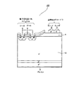
- FIG. 1 is a cross-sectional view showing the configuration of the superjunction semiconductor device according to the first embodiment of the present invention.
- FIG. 2 is a cross-sectional view of a main part showing the configuration of a MOS type semiconductor device having a conventional temperature detecting element.
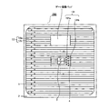
- FIG. 3 is a plan view showing the configuration of the superjunction semiconductor device according to the first embodiment of the present invention.
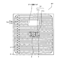
- FIG. 4 is a plan view showing the configuration of the superjunction semiconductor device according to the second embodiment of the present invention.
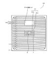
- FIG. 5 is a plan view showing the configuration of the superjunction semiconductor device according to the third embodiment of the present invention.
- FIG. 1 is a cross-sectional view showing the configuration of the superjunction semiconductor device according to the first embodiment of the present invention.
- FIG. 3 is a plan view showing the configuration of the superjunction semiconductor device according to the first embodiment of the present invention.
- 1 is a cross-sectional view taken along line AA ′ of FIG.
- the same reference numerals are given to portions common to FIG. 2.
- the superjunction semiconductor device according to the first embodiment of the present invention shown in FIGS. 1 and 3 is an SJ-MOSFET 200 including a temperature detecting element.
- This SJ-MOSFET 200 is provided on the same n + semiconductor substrate 6 with an element active portion 1 provided with a MOS gate structure 10 and a temperature detection element (hereinafter referred to as a temperature detection diode 3) including a diode 3. Temperature detection region 4 provided.
- the drift layer 12 includes a parallel pn in which n-type regions (hereinafter referred to as n drift regions) with high impurity concentration and p-type regions (hereinafter referred to as p partition regions) are alternately arranged. It consists of layers (SJ cells).
- a drift layer 12 under the MOS gate structure 10 in the element active portion 1 is provided with a main SJ cell 13.
- the temperature detection region 4 is provided in the element active portion 1.
- fine SJ cells 131 having a repetitive pitch narrower than the repetitive pitch of the main SJ cell 13 are provided in the drift layer 12 with the insulating film 5 interposed therebetween.
- FIG. 3 is a plan view of the entire SJ-MOSFET 200 including the temperature detection diode 3 according to the first embodiment of the present invention.
- the MOS gate structure 10 and the metal film (gate) on the surface of the parallel pn layer are clarified so that the plane pattern of the parallel pn layer (main SJ cell 13 and fine SJ cell 131) of the SJ-MOSFET 200 is clear.
- the electrode pad and the insulating film are not shown.
- this SJ-MOSFET 200 has a low resistance (high impurity concentration) n + semiconductor substrate 6 and a parallel pn layer (main SJ cell 13 and fine SJ cell 131) formed on the surface thereof. .
- the main SJ cell 13 is formed in the element active portion 1, and the fine SJ cell 131 is formed in the temperature detection region 4.
- N + semiconductor substrate 6 of the low resistance serves as the n + drain region, the metal electrode formed on the back surface of the n + drain region functions as the drain electrode 7.
- a laminated metal film such as titanium (Ti) -nickel (Ni) -gold (Au) that can be soldered is formed by a sputtering method or a vapor deposition method.
- a depletion layer rapidly spreads from each pn junction between the high impurity concentration n drift regions 13b and 131b and the p partition regions 13a and 131a to each region on both sides of the pn junction when off.
- width hereinafter simply referred to as width
- width in the direction in which both regions are aligned so that each region on both sides is completely depleted at low voltage, low on-voltage and high breakdown voltage can be achieved. Can be achieved.
- the arrangement pitch between the p partition region and the n drift region constituting each cell is different between the main SJ cell 13 and the fine SJ cell 131.
- the widths of the p partition region 131a and the n drift region 131b in the fine SJ cell 131 are narrower than the widths of the p partition region 13a and the n drift region 13b of the main SJ cell 13. The reason why the arrangement pitch of each region in the fine SJ cell 131 is made narrower than the arrangement pitch of each region of the main SJ cell 13 is to prevent a decrease in breakdown voltage.
- the n drift region 131b and the p partition region 131a of the parallel pn layer in the temperature detection region 4 have the same width or the same arrangement pitch as the n drift region 13b and the p partition region 13a of the parallel pn layer of the element active unit 1.
- the insulating film 5 of the parallel pn layer There arises a problem that the portion (top portion) in contact with the substrate is not sufficiently depleted. As a result, electric field concentration is likely to occur in a portion that is not depleted, and the breakdown voltage is reduced. Therefore, the fine SJ cell 131 is arranged with the above-described configuration.
- the main SJ cell 13 is composed of an n drift region 13b and a p partition region 13a which are repeatedly arranged adjacent to each other in a direction parallel to the main surface of the n + semiconductor substrate 6.
- the fine SJ cell 131 includes an n drift region 131 b and a p partition region 131 a that are arranged repeatedly adjacent to each other in a direction parallel to the main surface of the n + semiconductor substrate 6.
- the n drift regions 13 b and 131 b and the p partition regions 13 a and 131 a have a layer shape or a column shape having a narrow width and extending in a direction perpendicular to the main surface of the n + semiconductor substrate 6. As shown in FIG.
- the planar pattern of the n drift region 13b and the p partition region 13a in the element active portion 1 is, for example, a stripe extending in a direction orthogonal to the direction in which the n drift region 13b and the p partition region 13a are arranged.
- the n drift region 131b and the p partition region 131a in the temperature detection region 4 are also striped planar patterns extending in a direction orthogonal to the direction in which the n drift region 131b and the p partition region 131a are arranged as shown in FIG. It is.
- the n drift region 131b and the p partition region 131a in the temperature detection region 4 are parallel to the n drift region 13b and the p partition region 13a in the element active portion 1.
- the array pitch of the striped planar patterns of the n drift region 131b and the p partition region 131a is about one half of the array pitch of the striped planar patterns of the n drift region 13b and the p partition region 13a in the element active portion 1. Is preferred.
- the reason is that the interdiffusion between the n drift region 131b and the p partition region 131a in the temperature detection region 4 is increased, and the impurity concentration in both regions can be reduced by compensating the impurity concentration. It is because it becomes easy to spread.
- the extending directions of the striped planar patterns of the parallel pn layers of the element active portion 1 and the temperature detection region 4 are parallel to each other.
- a white rectangular region illustrated above the temperature detection region 4 in the element active portion 1 is a gate electrode pad portion.
- a breakdown voltage structure 2 that relaxes the electric field at the end of the element active portion 1 and holds the breakdown voltage is provided so as to surround the outer periphery of the element active portion 1.
- the breakdown voltage structure 2 is not different from the breakdown voltage structure of a conventional MOSFET, and thus a detailed description thereof is omitted.
- a p base region 14 is provided in the surface layer opposite to the n + semiconductor substrate 6 side of each p partition region 13 a in the same manner as a normal MOSFET. Inside the p base region 14, an n + source region 15 and a high concentration p + contact region 14a are provided so as to be exposed on the surface of the parallel pn layer opposite to the n + semiconductor substrate 6 side. Yes. On the surface of the portion of the p base region 14 sandwiched between the n + source region 15 and the n drift region 13b, a gate electrode 16 made of a polycrystalline silicon film is provided via a gate insulating film 5a.
- a source electrode 17 in common contact is provided on the surfaces of the n + source region 15 and the p + contact region 14a by a metal film mainly composed of aluminum (Al).
- the gate electrode 16 is covered by the interlayer insulating film 8 and further ensures electrical insulation from the source electrode 17 covering the interlayer insulating film 8.
- the temperature detection diode 3 is formed on the surface opposite to the n + semiconductor substrate 6 side of the fine SJ cell 131 through the thick insulating film 5.
- the temperature detection diode 3 is composed of a p + anode region and an n + cathode region deposited so as to be in contact with the surface of the insulating film 5, and has a pn junction between both regions.
- An anode electrode is provided on the surface of the p + anode region, and a cathode electrode is provided on the surface of the n + cathode region.
- the insulating film 5 is preferably as thick as possible in order to suppress mutual interference between the temperature detection diode 3 and the fine SJ cell 131.
- an insulating film 5 as an oxide film formed at the same time as a field oxide film formed as a protective film on the drift layer surface of the breakdown voltage structure portion 2 not shown in FIG. Since it becomes the same thickness as a film
- the temperature detection diode 3 is formed in a state where it is electrically insulated from the fine SJ cell 131 by the insulating film 5.
- an influence such as a field plate effect in the breakdown voltage structure portion 2 extends to the parallel pn layer (fine SJ cell 131) immediately below the insulating film 5.
- the depletion may be insufficient.
- the repetition pitch of the fine SJ cells 131 below the temperature detection diode 3 in the temperature detection region 4 is made narrower than the repetition pitch of the main SJ cells 13 in the element active unit 1, thereby preventing a reduction in breakdown voltage. Occurs.
- the SJ-MOSFET 200 according to the first embodiment has the conventional SJ-MOSFET 200.
- the breakdown voltage drop that has occurred in the SJ-MOSFET is prevented, and the breakdown voltage can be increased.
- the p base region 14 is not formed on the fine SJ cell 131 below the temperature detection region 4.
- the fine SJ cell 131 has a longer cell length in the direction perpendicular to the main surface of the n + semiconductor substrate 6 than the main SJ cell 13 because the p base region 14 is not formed.
- the effect of achieving a higher breakdown voltage than the element active portion 1 is also expected. Further, since the process for forming the p base region 14 in the temperature detection region 4 is not required, the manufacturing cost can be suppressed. Note that the temperature detection region 4 may not be arranged at the center of the element active portion 1 as shown in FIG. That is, the temperature detection region 4 may be provided anywhere in the element active portion 1.
- FIG. 4 is a plan view showing the configuration of the superjunction semiconductor device according to the second embodiment of the present invention.
- the difference between the SJ-MOSFET 300 according to the second embodiment and the SJ-MOSFET 200 according to the first embodiment is that the stripe-like planar pattern of the temperature detection region 4 and the stripe-like planar pattern of the element active portion 1 are orthogonal to each other. It is a point.
- the fine SJ cell 141 in the temperature detection region 4 is a striped planar pattern extending in a direction orthogonal to the direction in which the n drift region 141b and the p partition region 141a are arranged, as shown in FIG. The same as the fine SJ cell.
- the micro SJ cell 141 is different from the micro SJ cell shown in FIG. 3 in that the extending direction of the stripe of the planar pattern of the fine SJ cell 141 is orthogonal to the extending direction of the stripe of the planar pattern of the main SJ cell 13 of the element active portion 1. Even when the configuration of the fine SJ cell shown in FIG. 4 is adopted, the same effect as in the first embodiment can be obtained.
- the stripe-like plane patterns of the fine SJ cell 141 and the main SJ cell 13 orthogonal to each other the degree of freedom in designing the repeat pitch of the SJ cell is increased, miniaturization is facilitated, and higher breakdown voltage is facilitated. become.
- FIG. 5 is a plan view showing the configuration of the superjunction semiconductor device according to the third embodiment of the present invention.
- the SJ-MOSFET 400 according to the third embodiment is different from the SJ-MOSFETs 200 and 300 according to the first and second embodiments in that the fine SJ cell 151 in the temperature detection region 4 has a lattice-like planar pattern.
- the lattice-like planar pattern is a planar pattern in which, for example, p partition regions 151a having a rectangular planar shape are arranged in a matrix in the n drift region 151b.
- the fine SJ cell 151 has the same effect as that of the first embodiment by making the arrangement pitch of the lattice-like planar pattern narrower than the arrangement pitch of the stripe-like planar pattern of the main SJ cell 13. .
- a fine SJ cell having a repetitive pitch narrower than the repetitive pitch of the main SJ cell is disposed below the temperature detection diode in the temperature detection region via an insulating film.
- the present invention has been described by taking the SJ-MOSFET as an example.
- the present invention is not limited to the above-described embodiment, and can be applied to various superjunction semiconductor devices including a temperature detection diode.
- the first conductivity type is n-type and the second conductivity type is p-type.
- the first conductivity type is p-type and the second conductivity type is n-type. It holds.
- the superjunction semiconductor device according to the present invention is useful for a power semiconductor device used for a switching element that repeats an on / off operation.
Landscapes
- Metal-Oxide And Bipolar Metal-Oxide Semiconductor Integrated Circuits (AREA)
- Semiconductor Integrated Circuits (AREA)
- Chemical & Material Sciences (AREA)
- Composite Materials (AREA)
Abstract
Description
以下、本発明の実施の形態1にかかる超接合半導体装置について、SJ-MOSFETを例に詳細に説明する。図1は、本発明の実施の形態1にかかる超接合半導体装置の構成を示す断面図である。図3は、本発明の実施の形態1にかかる超接合半導体装置の構成を示す平面図である。図1は、図3のA-A’線における断面図である。図1,3において図2と共通の部分には同一の符号を付けている。図1,3に示す本発明の実施の形態1にかかる超接合半導体装置は、温度検出用素子を備えるSJ-MOSFET200である。このSJ-MOSFET200は、同一のn+半導体基板6上に、MOSゲート構造10が設けられた素子活性部1と、ダイオード3からなる温度検出用素子(以下、温度検出ダイオード3とする)が設けられた温度検出領域4とを備える。
図4は、本発明の実施の形態2にかかる超接合半導体装置の構成を示す平面図である。実施の形態2にかかるSJ-MOSFET300が実施の形態1にかかるSJ-MOSFET200とは異なる点は、温度検出領域4のストライプ状の平面パターンと素子活性部1のストライプ状の平面パターンとが直交している点である。図4に示すように、温度検出領域4内の微細SJセル141がnドリフト領域141b及びp仕切り領域141aが並ぶ方向と直交する方向に延びるストライプ状の平面パターンである点は、図3に示す微細SJセルと同様である。微細SJセル141の平面パターンのストライプの延びる方向が素子活性部1のメインSJセル13の平面パターンのストライプの延びる方向と直交する点が、図3に示す微細SJセルと異なる。図4に示す微細SJセルの構成とした場合においても、実施の形態1と同様の効果が得られる。微細SJセル141とメインSJセル13とのストライプ状の平面パターンを相互に直交させることにより、SJセルの繰り返しピッチの設計自由度が上がり、微細化が容易になるとともに、より高耐圧化が容易になる。
図5は、本発明の実施の形態3にかかる超接合半導体装置の構成を示す平面図である。実施の形態3にかかるSJ-MOSFET400が実施の形態1,2にかかるSJ-MOSFET200,300とは異なる点は、温度検出領域4内の微細SJセル151が格子状の平面パターンである点である。格子状の平面パターンとは、例えばnドリフト領域151b内に、矩形状の平面形状を有するp仕切り領域151aをマトリクス状に配置した平面パターンである。実施の形態3においても微細SJセル151は格子状の平面パターンの配列ピッチをメインSJセル13のストライプ状の平面パターンの配列ピッチより狭くすることにより、実施の形態1と同様の効果が得られる。
2 耐圧構造部
3 温度検出ダイオード
4 温度検出領域
5 絶縁膜
6 n+半導体基板
7 ドレイン電極
8 層間絶縁膜
10 MOSゲート構造
12 ドリフト層
13 メインSJセル
13a p仕切り領域
13b nドリフト領域
14 pベース領域
15 n+ソース領域
16 ゲート電極
17 ソース電極
131,141,151 微細SJセル
131a,141a,151a p仕切り領域
131b,141b,151b nドリフト領域
200,300,400 SJ-MOSFET
Claims (8)
- 第1導電型の高不純物濃度の半導体基板の一方の主面の垂直方向に配向する第1導電型半導体領域と第2導電型半導体領域とが、前記半導体基板の主面に平行な方向に所定のピッチで繰り返し交互に隣接する並列pn層をドリフト層として備え、前記第1導電型半導体領域にオン状態で電流を流し、オフ状態では前記並列pn層を空乏化して電圧を阻止する構成を有する超接合半導体装置であって、
主電流経路となる素子活性部と、
前記素子活性部内に設けられた、前記並列pn層の前記第1導電型半導体領域と前記第2導電型半導体領域とのピッチが前記所定のピッチよりも狭い温度検出領域と、
前記温度検出領域の前記並列pn層の表面に絶縁膜を介して設けられた第1導電型半導体層と、
前記温度検出領域の前記並列pn層の表面に絶縁膜を介して設けられ、前記第1導電型半導体層と接してpn接合を構成するように配置された第2導電型半導体層と、
前記第1導電型半導体層と前記第2導電型半導体層とを主たる半導体層とする温度検出用素子と、
を備えることを特徴とする超接合半導体装置。 - 前記素子活性部は絶縁ゲート構造を備え、
前記温度検出領域内の前記並列pn層の表面の前記絶縁膜が、前記絶縁ゲート構造を構成するゲート絶縁膜よりも厚いことを特徴とする請求項1に記載の超接合半導体装置。 - 前記素子活性部を囲むように前記素子活性部の外周に配置され、耐圧を保持する耐圧構造部をさらに備え、
前記温度検出領域内の前記並列pn層の表面の前記絶縁膜が、前記耐圧構造部の表面を保護するフィールド絶縁膜と同程度の厚さを有することを特徴とする請求項2に記載の超接合半導体装置。 - 前記温度検出領域内の前記並列pn層の平面パターンが、前記第1導電型半導体領域と前記第2導電型半導体領域とが並ぶ方向に直交する方向に延びるストライプ状であることを特徴とする請求項1に記載の超接合半導体装置。
- 前記素子活性部内の前記並列pn層の平面パターンが、前記第1導電型半導体領域と前記第2導電型半導体領域とが並ぶ方向に直交する方向に延びるストライプ状であり、
前記温度検出領域内の前記並列pn層のストライプ状の平面パターンが、前記素子活性部内の前記並列pn層のストライプ状の平面パターンに対して平行であることを特徴とする請求項4に記載の超接合半導体装置。 - 前記素子活性部内の前記並列pn層の平面パターンが、前記第1導電型半導体領域と前記第2導電型半導体領域とが並ぶ方向に直交する方向に延びるストライプ状であり、
前記温度検出領域内の前記並列pn層のストライプ状の平面パターンが、前記素子活性部内の前記並列pn層のストライプ状の平面パターンに対して直交していることを特徴とする請求項4に記載の超接合半導体装置。 - 前記温度検出領域内の前記並列pn層は、前記第1導電型半導体領域内に前記第2導電型半導体領域がマトリクス状に配置された平面パターンを有することを特徴とする請求項1に記載の超接合半導体装置。
- 前記温度検出用素子がポリシリコンであることを特徴とする請求項1~7のいずれか一つに記載の超接合半導体装置。
Priority Applications (4)
| Application Number | Priority Date | Filing Date | Title |
|---|---|---|---|
| JP2013525609A JP5720788B2 (ja) | 2011-07-22 | 2012-05-30 | 超接合半導体装置 |
| EP12818128.6A EP2736072B1 (en) | 2011-07-22 | 2012-05-30 | Superjunction semiconductor device |
| CN201280034308.7A CN103650141B (zh) | 2011-07-22 | 2012-05-30 | 超结半导体装置 |
| US14/079,101 US20140061644A1 (en) | 2011-07-22 | 2013-11-13 | Super-junction semiconductor device |
Applications Claiming Priority (2)
| Application Number | Priority Date | Filing Date | Title |
|---|---|---|---|
| JP2011-160756 | 2011-07-22 | ||
| JP2011160756 | 2011-07-22 |
Related Child Applications (1)
| Application Number | Title | Priority Date | Filing Date |
|---|---|---|---|
| US14/079,101 Continuation US20140061644A1 (en) | 2011-07-22 | 2013-11-13 | Super-junction semiconductor device |
Publications (1)
| Publication Number | Publication Date |
|---|---|
| WO2013015014A1 true WO2013015014A1 (ja) | 2013-01-31 |
Family
ID=47600874
Family Applications (1)
| Application Number | Title | Priority Date | Filing Date |
|---|---|---|---|
| PCT/JP2012/064007 Ceased WO2013015014A1 (ja) | 2011-07-22 | 2012-05-30 | 超接合半導体装置 |
Country Status (6)
| Country | Link |
|---|---|
| US (1) | US20140061644A1 (ja) |
| EP (1) | EP2736072B1 (ja) |
| JP (1) | JP5720788B2 (ja) |
| CN (1) | CN103650141B (ja) |
| TW (1) | TWI567975B (ja) |
| WO (1) | WO2013015014A1 (ja) |
Cited By (6)
| Publication number | Priority date | Publication date | Assignee | Title |
|---|---|---|---|---|
| JP2016171198A (ja) * | 2015-03-12 | 2016-09-23 | エスアイアイ・セミコンダクタ株式会社 | 半導体装置 |
| US9935169B2 (en) | 2015-08-11 | 2018-04-03 | Fuji Electric Co., Ltd. | Semiconductor device and method of manufacturing the same |
| JP2019068290A (ja) * | 2017-10-02 | 2019-04-25 | 京セラ株式会社 | チップ型圧電デバイス及びその製造方法 |
| US10276654B2 (en) | 2014-07-04 | 2019-04-30 | Fuji Electric Co., Ltd. | Semiconductor device with parallel PN structures |
| DE102014008894B4 (de) | 2013-06-14 | 2019-05-02 | Infineon Technologies Ag | Erfassungselement für Halbleiter |
| JP2020077734A (ja) * | 2018-11-07 | 2020-05-21 | 三菱電機株式会社 | 半導体装置およびその製造方法 |
Families Citing this family (16)
| Publication number | Priority date | Publication date | Assignee | Title |
|---|---|---|---|---|
| US9614043B2 (en) | 2012-02-09 | 2017-04-04 | Vishay-Siliconix | MOSFET termination trench |
| US9842911B2 (en) | 2012-05-30 | 2017-12-12 | Vishay-Siliconix | Adaptive charge balanced edge termination |
| JP6197294B2 (ja) * | 2013-01-16 | 2017-09-20 | 富士電機株式会社 | 半導体素子 |
| US9887259B2 (en) | 2014-06-23 | 2018-02-06 | Vishay-Siliconix | Modulated super junction power MOSFET devices |
| KR102098996B1 (ko) | 2014-08-19 | 2020-04-08 | 비쉐이-실리코닉스 | 초접합 금속 산화물 반도체 전계 효과 트랜지스터 |
| US9881997B2 (en) * | 2015-04-02 | 2018-01-30 | Fuji Electric Co., Ltd. | Semiconductor device and manufacturing method of semiconductor device |
| CN106560909B (zh) * | 2015-09-30 | 2019-05-28 | 中芯国际集成电路制造(上海)有限公司 | 测试结构及其形成方法、测试方法 |
| JP6805620B2 (ja) * | 2016-08-10 | 2020-12-23 | 富士電機株式会社 | 半導体装置 |
| JP6747195B2 (ja) * | 2016-09-08 | 2020-08-26 | 富士電機株式会社 | 半導体装置および半導体装置の製造方法 |
| JP7092188B2 (ja) * | 2018-04-19 | 2022-06-28 | 日産自動車株式会社 | 半導体装置及びその製造方法 |
| CN108878305B (zh) * | 2018-06-29 | 2020-09-25 | 上海华虹宏力半导体制造有限公司 | 超结器件的终端结构的耐压验证方法 |
| JP7080166B2 (ja) * | 2018-12-21 | 2022-06-03 | 三菱電機株式会社 | 半導体装置、および、半導体装置の製造方法 |
| CN113035949A (zh) * | 2019-12-25 | 2021-06-25 | 株洲中车时代半导体有限公司 | Igbt芯片 |
| JP7454454B2 (ja) * | 2020-06-18 | 2024-03-22 | ルネサスエレクトロニクス株式会社 | 半導体装置およびその製造方法 |
| WO2021260851A1 (ja) * | 2020-06-24 | 2021-12-30 | 三菱電機株式会社 | 半導体装置およびその製造方法 |
| CN112349715B (zh) * | 2020-11-05 | 2024-03-26 | 宁波宝芯源功率半导体有限公司 | 具有温度及电压检测功能的功率半导体器件及制作方法 |
Citations (4)
| Publication number | Priority date | Publication date | Assignee | Title |
|---|---|---|---|---|
| JPH06117942A (ja) | 1992-10-06 | 1994-04-28 | Fuji Electric Co Ltd | 半導体装置 |
| JP2006313892A (ja) * | 2005-04-07 | 2006-11-16 | Toshiba Corp | 半導体素子 |
| JP2006324432A (ja) | 2005-05-18 | 2006-11-30 | Fuji Electric Holdings Co Ltd | 半導体装置およびその製造方法 |
| JP2009147297A (ja) * | 2007-11-20 | 2009-07-02 | Denso Corp | Soi基板を用いた半導体装置およびその製造方法 |
Family Cites Families (26)
| Publication number | Priority date | Publication date | Assignee | Title |
|---|---|---|---|---|
| JPH0334360A (ja) * | 1989-06-29 | 1991-02-14 | Nec Corp | 半導体装置 |
| JP3982842B2 (ja) * | 1993-08-18 | 2007-09-26 | 株式会社ルネサステクノロジ | 半導体装置 |
| JP2701824B2 (ja) * | 1996-02-09 | 1998-01-21 | 株式会社デンソー | 半導体装置 |
| JP3911566B2 (ja) * | 1998-01-27 | 2007-05-09 | 富士電機デバイステクノロジー株式会社 | Mos型半導体装置 |
| JP4774580B2 (ja) * | 1999-08-23 | 2011-09-14 | 富士電機株式会社 | 超接合半導体素子 |
| JP4765012B2 (ja) * | 2000-02-09 | 2011-09-07 | 富士電機株式会社 | 半導体装置及びその製造方法 |
| JP3899231B2 (ja) * | 2000-12-18 | 2007-03-28 | 株式会社豊田中央研究所 | 半導体装置 |
| JP2002190575A (ja) * | 2000-12-21 | 2002-07-05 | Toyota Industries Corp | 半導体装置およびその製造方法 |
| JP2002208702A (ja) * | 2001-01-10 | 2002-07-26 | Mitsubishi Electric Corp | パワー半導体装置 |
| JP4140232B2 (ja) * | 2001-12-07 | 2008-08-27 | 株式会社デンソー | 半導体装置 |
| EP1469523B1 (en) * | 2003-04-18 | 2008-12-24 | STMicroelectronics S.r.l. | A junction electronic component and an integrated power device incorporating said component |
| JP4166627B2 (ja) * | 2003-05-30 | 2008-10-15 | 株式会社デンソー | 半導体装置 |
| US7541643B2 (en) * | 2005-04-07 | 2009-06-02 | Kabushiki Kaisha Toshiba | Semiconductor device |
| JP4921730B2 (ja) * | 2005-06-20 | 2012-04-25 | 株式会社東芝 | 半導体装置 |
| US8084815B2 (en) * | 2005-06-29 | 2011-12-27 | Fairchild Korea Semiconductor Ltd. | Superjunction semiconductor device |
| DE102007063721B4 (de) * | 2006-03-22 | 2014-05-08 | Denso Corporation | Schaltkreis mit einem Transistor und einer Ansteuerschaltung zur Ansteuerung des Transistors |
| JP2008177328A (ja) * | 2007-01-18 | 2008-07-31 | Denso Corp | 半導体装置およびその製造方法 |
| JP5309497B2 (ja) * | 2007-08-09 | 2013-10-09 | 富士電機株式会社 | 半導体装置 |
| JP5298488B2 (ja) * | 2007-09-28 | 2013-09-25 | 富士電機株式会社 | 半導体装置 |
| US8278731B2 (en) * | 2007-11-20 | 2012-10-02 | Denso Corporation | Semiconductor device having SOI substrate and method for manufacturing the same |
| US8089134B2 (en) * | 2008-02-06 | 2012-01-03 | Fuji Electric Sytems Co., Ltd. | Semiconductor device |
| JP5560538B2 (ja) * | 2008-05-22 | 2014-07-30 | 富士電機株式会社 | 半導体装置の製造方法 |
| US20120273916A1 (en) * | 2011-04-27 | 2012-11-01 | Yedinak Joseph A | Superjunction Structures for Power Devices and Methods of Manufacture |
| JP2011066184A (ja) * | 2009-09-17 | 2011-03-31 | Renesas Electronics Corp | 半導体装置、及びその製造方法 |
| CN102214689B (zh) * | 2010-04-06 | 2012-11-07 | 上海华虹Nec电子有限公司 | 超级结器件的终端保护结构及其制造方法 |
| JP5757101B2 (ja) * | 2011-02-17 | 2015-07-29 | 富士電機株式会社 | 超接合半導体素子 |
-
2012
- 2012-05-30 EP EP12818128.6A patent/EP2736072B1/en not_active Not-in-force
- 2012-05-30 CN CN201280034308.7A patent/CN103650141B/zh not_active Expired - Fee Related
- 2012-05-30 WO PCT/JP2012/064007 patent/WO2013015014A1/ja not_active Ceased
- 2012-05-30 JP JP2013525609A patent/JP5720788B2/ja not_active Expired - Fee Related
- 2012-07-19 TW TW101126043A patent/TWI567975B/zh not_active IP Right Cessation
-
2013
- 2013-11-13 US US14/079,101 patent/US20140061644A1/en not_active Abandoned
Patent Citations (4)
| Publication number | Priority date | Publication date | Assignee | Title |
|---|---|---|---|---|
| JPH06117942A (ja) | 1992-10-06 | 1994-04-28 | Fuji Electric Co Ltd | 半導体装置 |
| JP2006313892A (ja) * | 2005-04-07 | 2006-11-16 | Toshiba Corp | 半導体素子 |
| JP2006324432A (ja) | 2005-05-18 | 2006-11-30 | Fuji Electric Holdings Co Ltd | 半導体装置およびその製造方法 |
| JP2009147297A (ja) * | 2007-11-20 | 2009-07-02 | Denso Corp | Soi基板を用いた半導体装置およびその製造方法 |
Non-Patent Citations (1)
| Title |
|---|
| See also references of EP2736072A4 |
Cited By (8)
| Publication number | Priority date | Publication date | Assignee | Title |
|---|---|---|---|---|
| DE102014008894B4 (de) | 2013-06-14 | 2019-05-02 | Infineon Technologies Ag | Erfassungselement für Halbleiter |
| US10276654B2 (en) | 2014-07-04 | 2019-04-30 | Fuji Electric Co., Ltd. | Semiconductor device with parallel PN structures |
| JP2016171198A (ja) * | 2015-03-12 | 2016-09-23 | エスアイアイ・セミコンダクタ株式会社 | 半導体装置 |
| US9935169B2 (en) | 2015-08-11 | 2018-04-03 | Fuji Electric Co., Ltd. | Semiconductor device and method of manufacturing the same |
| US10026812B2 (en) | 2015-08-11 | 2018-07-17 | Fuji Electric Co., Ltd. | Semiconductor device and method of manufacturing the same |
| JP2019068290A (ja) * | 2017-10-02 | 2019-04-25 | 京セラ株式会社 | チップ型圧電デバイス及びその製造方法 |
| JP2020077734A (ja) * | 2018-11-07 | 2020-05-21 | 三菱電機株式会社 | 半導体装置およびその製造方法 |
| JP7055087B2 (ja) | 2018-11-07 | 2022-04-15 | 三菱電機株式会社 | 半導体装置およびその製造方法 |
Also Published As
| Publication number | Publication date |
|---|---|
| CN103650141B (zh) | 2016-06-29 |
| EP2736072A1 (en) | 2014-05-28 |
| JPWO2013015014A1 (ja) | 2015-02-23 |
| TW201316506A (zh) | 2013-04-16 |
| TWI567975B (zh) | 2017-01-21 |
| JP5720788B2 (ja) | 2015-05-20 |
| CN103650141A (zh) | 2014-03-19 |
| EP2736072B1 (en) | 2017-01-11 |
| US20140061644A1 (en) | 2014-03-06 |
| EP2736072A4 (en) | 2015-02-25 |
Similar Documents
| Publication | Publication Date | Title |
|---|---|---|
| JP5720788B2 (ja) | 超接合半導体装置 | |
| CN103022115B (zh) | 半导体装置 | |
| JP4839519B2 (ja) | 半導体装置 | |
| JP5509908B2 (ja) | 半導体装置およびその製造方法 | |
| CN102468337B (zh) | 半导体器件 | |
| JP6729003B2 (ja) | 半導体装置および半導体装置の製造方法 | |
| JP6009731B2 (ja) | 半導体装置 | |
| JP2013149761A (ja) | 半導体装置 | |
| JP5321377B2 (ja) | 電力用半導体装置 | |
| JPWO2019069580A1 (ja) | 半導体装置 | |
| JP7091693B2 (ja) | 半導体装置 | |
| JP5751763B2 (ja) | 半導体装置 | |
| JP6795032B2 (ja) | 半導体装置 | |
| JPWO2019017104A1 (ja) | 半導体装置 | |
| JP6277173B2 (ja) | 半導体装置 | |
| JP2024045650A (ja) | 炭化珪素半導体装置および炭化珪素半導体装置の製造方法 | |
| JP2020141003A (ja) | スイッチング素子とその製造方法 | |
| JP6278549B2 (ja) | 半導体装置 | |
| US20150221641A1 (en) | Semiconductor device | |
| JP2012004466A (ja) | 半導体装置 | |
| JP2021168334A (ja) | 半導体装置 | |
| JP2019054195A (ja) | 半導体装置 | |
| JP6289600B2 (ja) | 半導体装置 | |
| JP5884772B2 (ja) | 半導体装置 | |
| WO2024122162A1 (ja) | スイッチング素子 |
Legal Events
| Date | Code | Title | Description |
|---|---|---|---|
| 121 | Ep: the epo has been informed by wipo that ep was designated in this application |
Ref document number: 12818128 Country of ref document: EP Kind code of ref document: A1 |
|
| ENP | Entry into the national phase |
Ref document number: 2013525609 Country of ref document: JP Kind code of ref document: A |
|
| REEP | Request for entry into the european phase |
Ref document number: 2012818128 Country of ref document: EP |
|
| WWE | Wipo information: entry into national phase |
Ref document number: 2012818128 Country of ref document: EP |
|
| NENP | Non-entry into the national phase |
Ref country code: DE |