WO2013015348A1 - Diamant polycristallin, son procédé de fabrication, outil de rainurage, mollette de rainurage, molette, outil rotatif, orifice de jet d'eau, filière de tréfilage, outil de coupe et source d'électrons - Google Patents
Diamant polycristallin, son procédé de fabrication, outil de rainurage, mollette de rainurage, molette, outil rotatif, orifice de jet d'eau, filière de tréfilage, outil de coupe et source d'électrons Download PDFInfo
- Publication number
- WO2013015348A1 WO2013015348A1 PCT/JP2012/068932 JP2012068932W WO2013015348A1 WO 2013015348 A1 WO2013015348 A1 WO 2013015348A1 JP 2012068932 W JP2012068932 W JP 2012068932W WO 2013015348 A1 WO2013015348 A1 WO 2013015348A1
- Authority
- WO
- WIPO (PCT)
- Prior art keywords
- graphite
- polycrystalline diamond
- diamond
- carbon
- gas
- Prior art date
- Legal status (The legal status is an assumption and is not a legal conclusion. Google has not performed a legal analysis and makes no representation as to the accuracy of the status listed.)
- Ceased
Links
Images

Classifications
-
- C—CHEMISTRY; METALLURGY
- C01—INORGANIC CHEMISTRY
- C01B—NON-METALLIC ELEMENTS; COMPOUNDS THEREOF; METALLOIDS OR COMPOUNDS THEREOF NOT COVERED BY SUBCLASS C01C
- C01B32/00—Carbon; Compounds thereof
- C01B32/25—Diamond
-
- B—PERFORMING OPERATIONS; TRANSPORTING
- B01—PHYSICAL OR CHEMICAL PROCESSES OR APPARATUS IN GENERAL
- B01J—CHEMICAL OR PHYSICAL PROCESSES, e.g. CATALYSIS OR COLLOID CHEMISTRY; THEIR RELEVANT APPARATUS
- B01J3/00—Processes of utilising sub-atmospheric or super-atmospheric pressure to effect chemical or physical change of matter; Apparatus therefor
- B01J3/06—Processes using ultra-high pressure, e.g. for the formation of diamonds; Apparatus therefor, e.g. moulds or dies
- B01J3/062—Processes using ultra-high pressure, e.g. for the formation of diamonds; Apparatus therefor, e.g. moulds or dies characterised by the composition of the materials to be processed
-
- C—CHEMISTRY; METALLURGY
- C01—INORGANIC CHEMISTRY
- C01B—NON-METALLIC ELEMENTS; COMPOUNDS THEREOF; METALLOIDS OR COMPOUNDS THEREOF NOT COVERED BY SUBCLASS C01C
- C01B32/00—Carbon; Compounds thereof
- C01B32/25—Diamond
- C01B32/26—Preparation
-
- C—CHEMISTRY; METALLURGY
- C04—CEMENTS; CONCRETE; ARTIFICIAL STONE; CERAMICS; REFRACTORIES
- C04B—LIME, MAGNESIA; SLAG; CEMENTS; COMPOSITIONS THEREOF, e.g. MORTARS, CONCRETE OR LIKE BUILDING MATERIALS; ARTIFICIAL STONE; CERAMICS; REFRACTORIES; TREATMENT OF NATURAL STONE
- C04B35/00—Shaped ceramic products characterised by their composition; Ceramics compositions; Processing powders of inorganic compounds preparatory to the manufacturing of ceramic products
- C04B35/515—Shaped ceramic products characterised by their composition; Ceramics compositions; Processing powders of inorganic compounds preparatory to the manufacturing of ceramic products based on non-oxide ceramics
- C04B35/52—Shaped ceramic products characterised by their composition; Ceramics compositions; Processing powders of inorganic compounds preparatory to the manufacturing of ceramic products based on non-oxide ceramics based on carbon, e.g. graphite
-
- B—PERFORMING OPERATIONS; TRANSPORTING
- B01—PHYSICAL OR CHEMICAL PROCESSES OR APPARATUS IN GENERAL
- B01J—CHEMICAL OR PHYSICAL PROCESSES, e.g. CATALYSIS OR COLLOID CHEMISTRY; THEIR RELEVANT APPARATUS
- B01J2203/00—Processes utilising sub- or super atmospheric pressure
- B01J2203/06—High pressure synthesis
- B01J2203/0605—Composition of the material to be processed
- B01J2203/061—Graphite
-
- B—PERFORMING OPERATIONS; TRANSPORTING
- B01—PHYSICAL OR CHEMICAL PROCESSES OR APPARATUS IN GENERAL
- B01J—CHEMICAL OR PHYSICAL PROCESSES, e.g. CATALYSIS OR COLLOID CHEMISTRY; THEIR RELEVANT APPARATUS
- B01J2203/00—Processes utilising sub- or super atmospheric pressure
- B01J2203/06—High pressure synthesis
- B01J2203/065—Composition of the material produced
- B01J2203/0655—Diamond
-
- C—CHEMISTRY; METALLURGY
- C04—CEMENTS; CONCRETE; ARTIFICIAL STONE; CERAMICS; REFRACTORIES
- C04B—LIME, MAGNESIA; SLAG; CEMENTS; COMPOSITIONS THEREOF, e.g. MORTARS, CONCRETE OR LIKE BUILDING MATERIALS; ARTIFICIAL STONE; CERAMICS; REFRACTORIES; TREATMENT OF NATURAL STONE
- C04B2235/00—Aspects relating to ceramic starting mixtures or sintered ceramic products
- C04B2235/02—Composition of constituents of the starting material or of secondary phases of the final product
- C04B2235/30—Constituents and secondary phases not being of a fibrous nature
- C04B2235/42—Non metallic elements added as constituents or additives, e.g. sulfur, phosphor, selenium or tellurium
-
- C—CHEMISTRY; METALLURGY
- C04—CEMENTS; CONCRETE; ARTIFICIAL STONE; CERAMICS; REFRACTORIES
- C04B—LIME, MAGNESIA; SLAG; CEMENTS; COMPOSITIONS THEREOF, e.g. MORTARS, CONCRETE OR LIKE BUILDING MATERIALS; ARTIFICIAL STONE; CERAMICS; REFRACTORIES; TREATMENT OF NATURAL STONE
- C04B2235/00—Aspects relating to ceramic starting mixtures or sintered ceramic products
- C04B2235/02—Composition of constituents of the starting material or of secondary phases of the final product
- C04B2235/30—Constituents and secondary phases not being of a fibrous nature
- C04B2235/42—Non metallic elements added as constituents or additives, e.g. sulfur, phosphor, selenium or tellurium
- C04B2235/422—Carbon
- C04B2235/427—Diamond
-
- Y—GENERAL TAGGING OF NEW TECHNOLOGICAL DEVELOPMENTS; GENERAL TAGGING OF CROSS-SECTIONAL TECHNOLOGIES SPANNING OVER SEVERAL SECTIONS OF THE IPC; TECHNICAL SUBJECTS COVERED BY FORMER USPC CROSS-REFERENCE ART COLLECTIONS [XRACs] AND DIGESTS
- Y10—TECHNICAL SUBJECTS COVERED BY FORMER USPC
- Y10T—TECHNICAL SUBJECTS COVERED BY FORMER US CLASSIFICATION
- Y10T428/00—Stock material or miscellaneous articles
- Y10T428/29—Coated or structually defined flake, particle, cell, strand, strand portion, rod, filament, macroscopic fiber or mass thereof
- Y10T428/2982—Particulate matter [e.g., sphere, flake, etc.]
Definitions
- the present invention relates to polycrystalline diamond and a method for producing the same, a scribe tool, a scribe wheel, a dresser, a rotating tool, a water jet orifice, a wire drawing die, a cutting tool, and an electron emission source.
- Diamond to which a different element other than carbon is uniformly added hereinafter referred to as “heterogeneous element-added nanopolycrystalline diamond”
- group III element-added nanopolycrystalline diamond group V element-added nanopolycrystalline diamond
- the present invention relates to a method and various tools and electron emission sources using the polycrystalline diamond.
- nano-polycrystalline diamond sintered body has hardness exceeding natural single-crystal diamond and has excellent properties as a tool.
- the nano-polycrystalline diamond is originally an insulator, but by adding another element such as an appropriate dopant, further functions such as conductivity can be imparted to the diamond. Further, by appropriately selecting an element to be added to diamond, various characteristics such as optical characteristics, electrical characteristics, and mechanical characteristics of diamond can be changed.
- nanopolycrystalline diamond is originally an insulator, but conductivity can be imparted to diamond by adding an element serving as an acceptor to diamond.
- the above literature describes a method for synthesizing boron-added diamond.
- conductivity can be imparted to the diamond by adding an element serving as a donor to the diamond.
- an element serving as a donor for example, Japanese Unexamined Patent Application Publication No. 2010-222165 describes a diamond layer containing an element capable of imparting conductivity.
- electrons can be emitted from n-type diamond, but it has been impossible to obtain n-type diamond doped with a donor at a high concentration by high-temperature and high-pressure synthesis.
- CVD vapor phase synthesis
- an element solid as a dopant an oxide of the element as a dopant, a hydride, a compound such as a halide is used, but when these are used, The hydride, oxide, etc. of the dopant remain or produce a compound. Due to these catalytic actions, the diamond crystal grains after conversion may become abnormally large locally.
- the above-mentioned problem is a problem that can occur when a different element other than a dopant is added to diamond.
- Non-Patent Document 1 boron is dissolved in graphite by reacting graphite (graphite) and B 4 C.
- graphite graphite
- B 4 C graphite
- the graphite powder and the acceptor element powder such as boron are pulverized as finely as possible and selected strictly, and then mixed or further subjected to a heat reaction treatment, as in the case described above.
- the method which uses what was made as a raw material is mentioned.
- n-type conductivity can be imparted to diamond by adding an element serving as a donor to diamond.
- the diamond having n-type conductivity has electron emission characteristics as described above. Utilizing this characteristic, diamond having n-type conductivity can be used for, for example, an electron gun.
- Single crystal synthesis and gas phase synthesis are known as methods for producing conductive diamond. However, it is very difficult to produce nano-polycrystalline diamond having n-type conductivity in which a donor element is uniformly added by using either single crystal synthesis or vapor phase synthesis.
- the simplest method for adding donor atoms to diamond is to use graphite powder and donor element powder as fine as possible, pulverize them as closely as possible, and mix or further heat-react the raw materials. Is mentioned.
- diamond crystal grains are likely to grow partly rapidly, and it has been difficult to obtain nano-polycrystalline diamond having uniform nano-sized crystal grains.
- the present invention has been made in view of the above problems, and one object of the present invention is to provide a nano-polycrystalline diamond in which different elements other than carbon are uniformly added to diamond and a method for producing the same. It is in.
- Another object of the present invention is to provide nano-polycrystalline diamond in which an acceptor element is uniformly added to diamond at an unprecedented level and a production method thereof, a scribe tool using the polycrystalline diamond, a scribe wheel, a dresser, a rotary tool, It is an object to provide a water jet orifice, a wire drawing die, and a cutting tool.
- Still another object of the present invention is to provide nano polycrystalline diamond in which a donor element is uniformly added to diamond, a method for producing the same, and an electron emission source produced using the polycrystalline diamond.
- the polycrystalline diamond according to the present invention is composed of carbon, a different element which is added so as to be dispersed at an atomic level in the carbon and is an element other than carbon, and inevitable impurities.
- the crystal grain size of the polycrystalline diamond is about 500 nm or less.
- the heterogeneous elements are preferably dispersed in carbon as substitutional isolated atoms.
- the concentration of the different element is, for example, about 1 ⁇ 10 14 / cm 3 or more and 1 ⁇ 10 22 / cm 3 or less.
- the polycrystalline diamond can be produced by sintering graphite obtained by pyrolyzing a mixed gas of a gas containing different elements and a hydrocarbon gas at a temperature of 1500 ° C. or higher.
- the method for producing polycrystalline diamond according to the present invention comprises a step of preparing graphite in which a different element other than carbon is dispersed so as to be dispersed at an atomic level in carbon, and And performing a heat treatment to convert the graphite directly into diamond.
- the step of converting the graphite into diamond it is preferable to heat the graphite in a high-pressure press without adding a sintering aid or a catalyst.
- a mixed gas of a gas containing a different element and a hydrocarbon gas is introduced into a vacuum chamber, and the mixed gas is pyrolyzed at a temperature of 1500 ° C. or higher to add the different element onto the substrate. It may include a step of forming the performed graphite.
- the graphite formed on the substrate may be heated in a high-pressure press.
- the mixed gas is preferably flowed toward the surface of the substrate.
- methane gas can be used as the hydrocarbon gas.
- the polycrystalline diamond according to another aspect of the present invention is composed of carbon, a group III element added so as to be dispersed in the carbon at an atomic level, and unavoidable impurities.
- the crystal grain size (maximum length of crystal grains) of the polycrystalline diamond is about 500 nm or less.
- the group III element is preferably dispersed in carbon as a substitutional isolated atom.
- the concentration of the group III element is, for example, about 1 ⁇ 10 14 / cm 3 or more and about 1 ⁇ 10 22 / cm 3 or less.
- the polycrystalline diamond can be produced by sintering graphite obtained by pyrolyzing a mixed gas of a gas containing a group III element and a hydrocarbon gas at a temperature of 1500 ° C. or higher.
- a method for producing polycrystalline diamond according to another aspect of the present invention includes a step of preparing graphite in which a group III element is dispersed in carbon at an atomic level, and a heat treatment of the graphite in a high-pressure press apparatus. And converting the graphite into diamond.
- the step of converting the graphite into diamond it is preferable to heat-treat the graphite in a high-pressure press without adding a sintering aid or a catalyst.
- the step of preparing the graphite is to introduce a mixed gas of a group III element-containing gas and a hydrocarbon gas into a vacuum chamber, and thermally decompose the mixed gas at a temperature of 1500 ° C. or higher to form graphite on the substrate.
- the process to perform may be included.
- the graphite formed on the substrate may be subjected to heat treatment at 1500 ° C. or higher under a high pressure of 8 GPa or higher.
- the mixed gas is preferably flowed toward the surface of the substrate.
- methane gas can be used as the hydrocarbon gas.
- the above polycrystalline diamond can be used for various tools. Specifically, the polycrystalline diamond can be used for a scribe tool, a scribe wheel, a dresser, a rotating tool, a water jet orifice, a wire drawing die, and a cutting tool.
- the polycrystalline diamond according to still another aspect of the present invention is composed of carbon, a group V element added so as to be dispersed at an atomic level in the carbon, and unavoidable impurities.
- the crystal grain size of the polycrystalline diamond is about 500 nm or less.
- the group V elements are preferably dispersed in carbon as substitutional isolated atoms.
- the concentration of the group V element is, for example, about 1 ⁇ 10 14 / cm 3 or more and 1 ⁇ 10 22 / cm 3 or less.
- the polycrystalline diamond can be produced by sintering graphite obtained by pyrolyzing a mixed gas of a gas containing a group V element and a hydrocarbon gas at a temperature of 1500 ° C. or higher.
- a method for producing polycrystalline diamond according to still another aspect of the present invention includes a step of preparing graphite having a crystal grain size of 10 ⁇ m or less, wherein a group V element is added so as to be dispersed at an atomic level in carbon, and a high temperature And subjecting the graphite to heat treatment in a high-pressure press to convert the graphite to diamond.
- the step of converting the graphite into diamond it is preferable to heat treat the graphite in a high-temperature and high-pressure press without adding a sintering aid or a catalyst.
- a mixed gas of a gas containing a group V element and a hydrocarbon gas is introduced into a vacuum chamber, and the mixed gas is pyrolyzed at a temperature of 1500 ° C. or more to form graphite on the substrate.
- the process to perform may be included.
- the step of converting the graphite into diamond the graphite formed on the substrate may be subjected to heat treatment in a high-temperature and high-pressure press.
- the mixed gas is preferably flowed toward the surface of the substrate.
- methane gas can be used as the hydrocarbon gas.
- the electron emission source according to the present invention is manufactured using the above-mentioned polycrystalline diamond.
- the different elements are added so as to be dispersed at the atomic level in the carbon, so that the different elements can be added to the diamond with an unprecedented level of uniformity.
- the heterogeneous element other than carbon is subjected to a heat treatment so as to disperse in the carbon at an atomic level and converted to polycrystalline diamond. Therefore, it is possible to produce polycrystalline diamond in which different elements are uniformly added at an unprecedented level.
- the group III element is added so as to be dispersed at an atomic level in carbon, the group III element is added to the diamond with an unprecedented level of uniformity. And p-type conductivity can be imparted to the nano-polycrystalline diamond.
- the graphite added with the group III element dispersed in carbon at an atomic level is subjected to a heat treatment to be converted into polycrystalline diamond. Therefore, nanopolycrystalline diamond in which a group III element is uniformly added can be produced at an unprecedented level, and p-type conductivity can be imparted to the nanopolycrystalline diamond.
- the polycrystalline diamond according to the present invention has excellent oxidation resistance, it is useful for tools such as a scribe tool, a scribe wheel, a dresser, a rotating tool, a water jet orifice, a wire drawing die, and a cutting tool.
- the group V element is added so as to be dispersed at an atomic level in the carbon. Therefore, the group V element is added to the diamond with an unprecedented level of uniformity. N-type conductivity can be imparted to the polycrystalline diamond.
- graphite having a crystal grain size of 10 ⁇ m or less is added in such a manner that a group V element is dispersed at an atomic level in carbon in a high-temperature and high-pressure press. Since it is converted into polycrystalline diamond by heat treatment, it is possible to produce polycrystalline diamond in which a group V element is uniformly added at an unprecedented level. Conventionally, particles of a few microns are segregated at least, but in the present invention, compounds other than diamond segregate even when using a high-intensity X-ray facility such as Spring 8 at a level that cannot be separated with a resolution of a few microns.
- the group V element can be uniformly added to the diamond so that the group V element exists as a substitutional element at the carbon position at an atomic level. Further, n-type conductivity can be imparted to the polycrystalline diamond, and the polycrystalline diamond has electron emission characteristics.
- the electron emission source according to the present invention is manufactured using the above-mentioned polycrystalline diamond, it has both excellent electron emission characteristics and durability.
- the different element-added nano-polycrystalline diamond in the present embodiment includes a different element added so as to be dispersed at the atomic level in carbon constituting the polycrystalline diamond body.
- the “heterogeneous element” refers to an element that can be added to diamond and is an element other than carbon constituting diamond and not an inevitable impurity contained in diamond.
- the different elements include nitrogen, hydrogen, group III elements, group V elements, silicon, metals such as transition metals, rare earths, and the like.
- a different element may be added to diamond alone, or a plurality of different elements may be added to diamond at the same time.
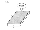
- the nano-polycrystalline diamond 1 of the present embodiment includes a heterogeneous element 3 that is formed on a substrate 2 and uniformly dispersed at the atomic level.
- “dispersing at an atomic level” means, for example, when solid carbon is produced by mixing carbon and a heterogeneous element in a gas phase to solidify in a vacuum atmosphere.
- the dispersion state at a level where different elements are dispersed in the solid carbon that is, this state is a state in which no isolated element or compound other than diamond is formed.
- the nano-polycrystalline diamond 1 can be produced by subjecting graphite formed on a base material to a heat treatment.
- Graphite is an integral solid and includes a crystallized portion.
- the polycrystalline diamond 1 has a flat plate shape, but it can be considered to have an arbitrary shape and thickness.
- the nano-polycrystalline diamond 1 and the graphite basically have the same shape.
- the above-mentioned different elements can be added to the graphite at the stage of forming the graphite.
- a mixed gas of a gas containing a different element and a hydrocarbon gas is thermally decomposed at a temperature of 1500 ° C. or more to form graphite on the base material, and at the same time, the different element can be added to the graphite.
- the different elements can be uniformly added to the graphite at the atomic level.
- a desired amount of the different element can be uniformly added at the atomic level.
- the thermal decomposition of the mixed gas can be carried out in a vacuum chamber, and at this time, by setting the degree of vacuum in the vacuum chamber to be relatively high, mixing of impurities into graphite can be suppressed.
- unintended inevitable impurities are mixed in the graphite.
- the inevitable impurities include nitrogen, hydrogen, oxygen, boron, silicon, transition metals, and the like, and elements other than the above different elements can be used.
- the amount of each inevitable impurity is about 0.01% by mass or less. That is, the concentration of inevitable impurities in graphite is about the detection limit or less in SIMS (Secondary Ion Mass Spectrometry) analysis. Moreover, about the transition metal, the density
- ICP Inductively Coupled Plasma
- the nano-polycrystalline diamond of the present embodiment uniformly contains different elements at the atomic level as described above, and the amount of impurities is extremely small.
- atoms of different elements in carbon do not aggregate in a cluster shape, and are in a state of being distributed almost uniformly throughout the entire diamond. Ideally, the atoms of the different elements exist in the carbon in an isolated state.
- the nano-polycrystalline diamond of the present embodiment includes the different elements dispersed at the atomic level in carbon, nano-polycrystalline diamond in which the different elements are uniformly added can be obtained at an unprecedented level. .
- different elements can be uniformly dispersed in the nano-polycrystalline diamond at the atomic level, desired characteristics and functions can be effectively imparted to the diamond.
- the addition of appropriate elements can improve the diamond's mechanical properties, such as effectively increasing the wear resistance of the diamond, and improve the electrical properties of the diamond, such as imparting conductivity to the diamond. It is also possible to improve the optical properties of the diamond by, for example, uniformly coloring the diamond.
- nitrogen can be selected as the different element.
- nitrogen can be dispersed in the diamond at the atomic level. That is, nitrogen atoms can be isolated and introduced into diamond. At this time, the nitrogen atoms are present in the carbon (diamond body) in a state where the nitrogen atoms are substituted. That is, the nitrogen atom is not simply mixed in the carbon, but is in a state in which the nitrogen atom and the carbon atom are chemically bonded.
- nano-polycrystalline diamond of the present embodiment to which nitrogen is added, nitrogen is dispersed in the diamond at the atomic level, so that there is almost no nitrogen mixed in the diamond in an aggregated state. Therefore, when the nano-polycrystalline diamond is irradiated with an electron beam and heated at 600 ° C. or higher, the diamond can be colored red or the like. Further, the added nitrogen does not aggregate at the crystal grain boundaries of diamond, and since there are very few impurities in diamond, abnormal growth of diamond crystals can be effectively suppressed. As a result, colored nano-polycrystalline diamond is obtained while being a polycrystalline body having a crystal grain size (maximum length of crystal grains) of 10 to 500 nm.
- the above-mentioned different elements such as nitrogen are dispersed at the atomic level in the diamond body, so that the concentration distribution of the different elements in the diamond hardly occurs. Also from this, local abnormal growth of diamond crystal grains can be effectively suppressed. As a result, compared with the conventional example, the size of diamond crystal grains can be made uniform.
- the concentration of the different elements in the diamond can be arbitrarily set.
- the concentration of different elements can be increased or decreased. In either case, since different elements can be dispersed in diamond at the atomic level, it is possible to effectively suppress the concentration distribution of different elements in diamond.
- the added concentration of the different elements is preferably in the range of about 10 14 to 10 22 / cm 3 in total in order to keep the crystal grain size of the polycrystalline diamond in the range of about 10 to 500 nm.
- the substrate is heated to a temperature of about 1500 ° C. to 3000 ° C. in a vacuum chamber.
- a well-known method can be adopted as the heating method.
- the base material any metal, inorganic ceramic material, or carbon material can be used as long as it can withstand a temperature of about 1500 ° C. to 3000 ° C.
- the base material is preferably made of carbon from the viewpoint of preventing impurities from being mixed into the raw material graphite. More preferably, it is conceivable that the base material is composed of diamond or graphite with very few impurities. In this case, at least the surface of the substrate may be composed of diamond or graphite.
- a hydrocarbon gas and a gas containing a different element are introduced into the vacuum chamber.
- the degree of vacuum in the vacuum chamber is set to about 20 to 100 Torr.
- the hydrocarbon gas and the gas containing the different element can be mixed in the vacuum chamber, and the graphite in which the different element is taken in at the atomic level can be formed on the heated substrate.
- unnecessary components do not remain.
- the base material may be heated after the introduction of the mixed gas to form graphite containing a different element on the base material.
- the hydrocarbon gas for example, methane gas can be used.
- methane gas can be used as the gas containing a different element.
- the gas containing a different element it is preferable to employ a hydride of a different element or a gas of an organic compound.
- a hydride as a different element, the hydride of a different element can be easily decomposed at a high temperature.
- an organic compound as the different element, a state in which the different element is surrounded by carbon, that is, a state where the different elements are isolated from each other can be obtained. Thereby, it becomes easy to take in different elements into graphite in an isolated state.
- a gas of methylamine or the like can be used.
- methane gas and methylamine gas are bubbled with argon gas to make a mixed gas, the mixed gas can be introduced into the vacuum chamber at a ratio of 10 ⁇ 7 % to 100%.
- each gas can be mixed efficiently near a base material, and the graphite containing a different element can be efficiently produced
- the hydrocarbon gas and the heterogeneous element-containing gas may be supplied from directly above the base material toward the base material, or may be supplied toward the base material from an oblique direction or a horizontal direction. It is also conceivable to install a guide member that guides a hydrocarbon gas or a gas containing a different element to the base material in the vacuum chamber.
- Sintered graphite in a high-pressure press machine which is manufactured as described above and added so that different elements, other than carbon, are dispersed at the atomic level in carbon, can be dissimilar at an unprecedented level. It is possible to produce a nano-polycrystalline diamond doped with different elements in which elements are uniformly added. That is, nano-polycrystalline diamond having nano-sized crystal grains is obtained after sintering of graphite.
- the crystal grain size of polycrystalline diamond can be about 10 to 500 nm.
- the step of converting graphite to diamond it is preferable to heat treat graphite under high pressure without adding a sintering aid or a catalyst.
- the graphite formed on the substrate may be subjected to heat treatment in an ultrahigh pressure apparatus.
- elements that are usually difficult to add to diamond can be confined in an isolated state in the diamond crystal by rapid crystal formation.
- the graphite that can be used for producing the nano-polycrystalline diamond according to the present embodiment is, for example, crystalline or polycrystalline that partially includes a crystallized portion.
- the density of graphite is preferably greater than 0.8 g / cm 3 . Thereby, the volume change at the time of sintering graphite can be made small. Also, from the viewpoint of improving the yield by reducing the volume change when graphite is sintered, the density of graphite should be about 1.4 g / cm 3 or more and 2.0 g / cm 3 or less experimentally. Is more preferable.
- the density of the graphite is within the above range is that when the density of the graphite is lower than 1.4 g / cm 3 , the volume change during the high-temperature and high-pressure process is too large, and the temperature control may not be possible. It is possible. Moreover, if the density of graphite is larger than 2.0 g / cm 3 , the probability that diamond will crack may be doubled or more.
- Methane gas and methylamine were mixed 1: 1 in a vacuum chamber, and the mixed gas was sprayed onto a diamond substrate heated to 1900 ° C. At this time, the degree of vacuum in the vacuum chamber was set to 20 to 30 Torr. Then, graphite containing nitrogen was deposited on the substrate. The bulk density of this graphite was 2.0 g / cm 3 .
- the above graphite was converted to diamond at a synthesis temperature of 2300 ° C. and 15 GPa to obtain nano-polycrystalline diamond to which nitrogen was added.
- the crystal grain size of the polycrystalline diamond was 10 to 200 nm.
- red nanopolycrystalline diamond was obtained.
- Methane gas and trimethylamine were mixed 1: 1 in a vacuum chamber, and the mixed gas was sprayed onto a diamond substrate heated to 1900 ° C. At this time, the degree of vacuum in the vacuum chamber was set to 20 to 30 Torr. Then, graphite containing nitrogen was deposited on the substrate. The bulk density of this graphite was 2.0 g / cm 3 . According to ICP elemental analysis, the nitrogen concentration in the graphite was 100 ppm.
- the above graphite was converted to diamond at a synthesis temperature of 2300 ° C. and 15 GPa to obtain nano-polycrystalline diamond to which nitrogen was added.
- the crystal grain size of the polycrystalline diamond was 10 to 200 nm.
- this polycrystalline diamond was irradiated with an electron beam and annealed at a high temperature of 800 ° C., a light red nano-polycrystalline diamond was obtained.
- Methane gas and methylamine were mixed 1: 1 in a vacuum chamber, and the mixed gas was sprayed onto a diamond substrate heated to 1900 ° C. At this time, the degree of vacuum in the vacuum chamber was 100 Torr. Then, graphite containing nitrogen was deposited on the substrate. The bulk density of this graphite was 2.0 g / cm 3 . According to ICP elemental analysis, the nitrogen concentration in the graphite was 100 ppm.
- the above graphite was converted to diamond at a synthesis temperature of 2300 ° C. and 15 GPa to obtain nano-polycrystalline diamond to which nitrogen was added.
- the crystal grain size of the polycrystalline diamond was 10 to 200 nm.
- red nanopolycrystalline diamond was obtained.
- Methane gas and trimethylamine were mixed 1: 1 in a vacuum chamber, and the mixed gas was sprayed onto a diamond substrate heated to 1900 ° C. At this time, the degree of vacuum in the vacuum chamber was 100 Torr. Then, graphite containing nitrogen was deposited on the substrate. The bulk density of this graphite was 2.0 g / cm 3 . According to ICP elemental analysis, the nitrogen concentration in the graphite was 150 ppm.
- the above graphite was converted to diamond at a synthesis temperature of 2300 ° C. and 15 GPa to obtain nano-polycrystalline diamond to which nitrogen was added.
- the crystal grain size of the polycrystalline diamond was 10 to 200 nm.
- this polycrystalline diamond was irradiated with an electron beam and annealed at a high temperature of 800 ° C., a light red nano-polycrystalline diamond was obtained.
- the degree of vacuum in the vacuum chamber is set to 20 to 100 Torr, and a hydrocarbon gas and a gas containing nitrogen are mixed in the vacuum chamber and heated to a temperature of about 1900 ° C.
- a graphite in which nitrogen was dispersed at an atomic level and having a bulk density of about 2.0 g / cm 3 in a solid phase could be produced on the substrate.
- the graphite into diamond at a synthesis temperature of 2300 ° C. and 15 GPa, nitrogen is dispersed at the atomic level, and the crystal grain size (maximum length of crystal grains) is about 10 to 200 nm. It was also confirmed that polycrystalline diamond could be produced. However, even under conditions other than those described above, it is considered that nanopolycrystalline diamond having excellent characteristics can be produced within the scope described in the claims.
- the group III element-added nanopolycrystalline diamond in the present embodiment includes a group III element added so as to be dispersed at the atomic level in carbon constituting the polycrystalline diamond body.
- the nano-polycrystalline diamond of the present embodiment is a polycrystalline diamond having a nano-sized crystal grain size that does not use a binder.
- the group III element is an element that can take a bond with one electron less than carbon, and is an element that serves as an acceptor in diamond.
- Examples of the group III element include boron, aluminum, gallium, indium, and thallium. One or more elements selected from these elements can be used, but other elements having the same function may be used. Among group III elements, boron is preferred, but it is also possible to use mixed elements in combination with boron and other elements.
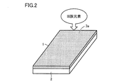
- the nano-polycrystalline diamond 1 of the present embodiment includes a group III element 3a formed on the substrate 2 and uniformly dispersed at the atomic level.
- group III element is dispersed at an atomic level means, for example, that carbon and a group III element are mixed in a gas phase in a vacuum atmosphere to solidify solid carbon. When produced, it means a dispersion state at a level where group III elements are dispersed in the solid carbon.
- the nano-polycrystalline diamond 1 can be produced by subjecting graphite formed on a base material to heat treatment under high temperature and high pressure.
- Graphite is an integral solid and includes a crystallized portion.
- the nanopolycrystalline diamond 1 has a flat plate shape, but it may be an arbitrary shape and thickness.
- the nano-polycrystalline diamond 1 and the graphite basically have the same shape.
- the group III element can be added to the graphite during the formation of the graphite. Specifically, a mixed gas of a gas containing a group III element and a hydrocarbon gas is pyrolyzed at a temperature of 1500 ° C. or higher to form graphite on the substrate, and at the same time, a group III element is added to the graphite. Can do.
- Examples of the gas containing the group III element include a first gas composed of a hydride of a group III element, and an organometallic second gas composed of one or more gases selected from trimethyl boron, triethyl boron, and trimethyl borate.
- An organometallic third gas composed of one or more gases selected from trimethylaluminum, triethylaluminum, dimethylaluminum hydride and triisobutylaluminum, an organometallic composed of one or more gases selected from trimethylgallium and triethylgallium
- a fourth gas of the system an organometallic fifth gas composed of one or more gases selected from trimethylindium and triethylindium
- an organometallic system composed of one or more gases selected from trimethylthallium and triethylthallium Use one of the sixth gases Possible it is. It is also conceivable to appropriately mix two or more of the above gases.
- the group III element As described above, by adding a group III element to the graphite forming raw material gas in the gas phase and adding the group III element to the graphite, the group III element is uniformly added to the graphite at the atomic level. can do. Further, by appropriately adjusting the addition amount of the gas containing the group III element to the hydrocarbon gas, a desired amount of the group III element can be added to the graphite.
- the thermal decomposition of the mixed gas can be carried out in a vacuum chamber, and at this time, by setting the degree of vacuum in the vacuum chamber to be relatively high, mixing of impurities into the graphite can be suppressed.
- unintended inevitable impurities are mixed in the graphite.
- the inevitable impurities include nitrogen, hydrogen, oxygen, silicon, transition metals, and the like, and elements other than the above group III elements that are intended to be added.
- the amount of each inevitable impurity is about 0.01% by mass or less. That is, the concentration of inevitable impurities in graphite is about the detection limit or less in SIMS (Secondary Ion Mass Spectrometry) analysis. Moreover, about the transition metal, the density
- ICP Inductively Coupled Plasma
- FIG. 3 shows an example of boron and impurity distribution in nano-polycrystalline diamond in the present embodiment.
- the boron-added nanopolycrystalline diamond shown in FIG. 3 was obtained by heat-treating graphite containing boron, which is a group III element, at 2000 ° C.
- B 4 C as a boron source and graphite prepared by a conventional method are mixed and heat-treated at 2000 ° C. in a vacuum atmosphere of 10 ⁇ 2 Pa to fix boron to the graphite.
- the result of comparing the mixing ratio of B 4 C between the boron-doped nanopolycrystalline diamond obtained by melting and the boron-doped nanopolycrystalline diamond of the present embodiment is shown.
- the B 4 C mixing rate increases as the concentration of boron added increases. It can be seen that in the form of boron-doped nanopolycrystalline diamond, even when the boron concentration to be added increases, the B 4 C mixing rate is extremely low, less than 0.01% by mass.
- the nano-polycrystalline diamond of the present embodiment contains a group III element uniformly at the atomic level as described above, but has an extremely small amount of impurities.
- atoms of group III elements do not aggregate in a cluster shape in carbon, and are in a state of being almost uniformly dispersed throughout the diamond.
- the atoms of the group III element are present in isolation from each other in the carbon.
- Group III element atoms are present in carbon (diamond body) in a state of substitution with carbon atoms, and are not simply mixed in carbon, but group III element atoms and carbon atoms are chemically bonded. It becomes the state that did.
- the nanopolycrystalline diamond of the present embodiment includes a group III element dispersed at an atomic level in carbon, the nanopolycrystalline diamond in which the group III element is uniformly added at an unprecedented level is provided. can get. Further, since the group III element can be uniformly dispersed at the atomic level in the nanopolycrystalline diamond, desired p-type conductivity can be imparted over the entire diamond.
- the group III element is dispersed in the diamond at the atomic level, so that the group III element mixed in the diamond in an aggregated state as described above Almost does not exist. Further, the added group III element does not aggregate at the crystal grain boundary of diamond, and the impurities in the diamond are extremely small, so that abnormal growth of the diamond crystal can be effectively suppressed. As a result, nano-polycrystalline diamond having a nano-sized crystal grain size (maximum crystal grain length) of 10 to 500 nm and p-type conductivity is obtained.
- the concentration distribution of group III elements in the diamond is difficult to occur. Also from this, local abnormal growth of diamond crystal grains can be effectively suppressed. As a result, compared with the conventional example, the size of diamond crystal grains can be made uniform.
- the concentration of group III elements in diamond can be arbitrarily set. It is possible to increase or decrease the concentration of the group III element in diamond. In any case, since the group III element can be uniformly dispersed in the diamond, it is possible to effectively suppress the concentration distribution of the group III element in the diamond. Thereby, it is possible to effectively suppress the occurrence of variation in local conductivity of diamond.
- the concentration of the Group III element is preferably in the range of about 10 14 to 10 22 / cm 3 in order to impart p-type conductivity to diamond.
- the group III element addition concentration is preferably about 10 19 / cm 3 or more, and in order to impart semiconductivity to diamond, a group III element The addition concentration of is preferably about 10 14 to less than 10 19 / cm 3 .
- the group III element-added nanopolycrystalline diamond of the present embodiment has the same hardness as the non-doped nanopolycrystalline diamond and has p-type conductivity.
- a cutting tool is manufactured using the nano-polycrystalline diamond of this embodiment, it has been found that it has cutting performance and life (wear resistance) equivalent to or higher than that of non-doped nano-polycrystalline diamond while having conductivity. It was. Further, when the insulating material is cut, the nano-polycrystalline diamond has conductivity, so that there is an advantage that adhesion of shavings due to static electricity is suppressed.
- the use of the nanopolycrystalline diamond of the present embodiment will be described in detail later.
- the substrate is heated to a temperature of about 1500 ° C. to 3000 ° C. in a vacuum chamber.
- a well-known method can be adopted as the heating method.
- the base material any metal, inorganic ceramic material, or carbon material can be used as long as it can withstand a temperature of about 1500 ° C. to 3000 ° C.
- the base material is preferably made of carbon from the viewpoint of preventing impurities from being mixed into the raw material graphite. More preferably, it is conceivable that the base material is composed of diamond or graphite with very few impurities. In this case, at least the surface of the substrate may be composed of diamond or graphite.
- a hydrocarbon gas and a gas containing a group III element are introduced into the vacuum chamber.
- the degree of vacuum in the vacuum chamber is set to about 20 to 100 Torr.
- hydrocarbon gas and the gas containing a group III element can be mixed within a vacuum chamber.
- graphite in which a group III element is taken in at an atomic level can be formed on the substrate.
- the base material may be heated after introducing the mixed gas to form graphite containing a group III element on the base material.
- methane gas can be used as the hydrocarbon gas.
- the gas containing a group III element the various gases described above can be used.
- a mixed gas of a hydrocarbon gas and a gas containing a group III element can be introduced into the vacuum chamber at a ratio of 10 ⁇ 7 % to 100%, for example.
- a hydrocarbon gas and a gas containing a group III element During the formation of graphite, it is preferable to flow a hydrocarbon gas and a gas containing a group III element toward the surface of the substrate. Thereby, each gas can be mixed efficiently in the vicinity of the substrate, and graphite containing a group III element can be efficiently generated on the substrate.
- the hydrocarbon gas and the group III element-containing gas may be supplied from directly above the base material toward the base material, or may be supplied from the oblique direction or the horizontal direction toward the base material. It is also conceivable to install a guide member that guides hydrocarbon gas or group III element-containing gas to the base material in the vacuum chamber.
- the step of converting graphite to diamond it is preferable to heat treat graphite under high pressure without adding a sintering aid or catalyst.
- the graphite formed on the substrate may be subjected to heat treatment at a high temperature and high pressure of 8 GPa or more and 1500 ° C. or more.
- the graphite that can be used for producing the nano-polycrystalline diamond according to the present embodiment is, for example, crystalline or polycrystalline that partially includes a crystallized portion.
- the density of graphite is preferably greater than 0.8 g / cm 3 . Thereby, the volume change at the time of sintering graphite can be made small. Also, from the viewpoint of improving the yield by reducing the volume change when graphite is sintered, the density of graphite should be about 1.4 g / cm 3 or more and 2.0 g / cm 3 or less experimentally. Is more preferable.
- the density of the graphite is within the above range is that when the density of the graphite is lower than 1.4 g / cm 3 , the volume change during the high-temperature and high-pressure process is too large, and the temperature control may not be possible. It is possible. Moreover, if the density of graphite is larger than 2.0 g / cm 3 , the probability that diamond will crack may be doubled or more.
- a trivalent atom occupies a part of tetravalent carbon.
- the number of covalently bonded electrons becomes insufficient in the system, but the diamond structure can be maintained by obtaining electrons from the outside.
- n-type diamond when the donor is activated and emits electrons, the electrons occupy the conduction state, that is, the energy state created by banding of antibonding orbitals. For this reason, it is considered that the diamond bond tends to be weakened.
- the nano-polycrystalline diamond of the present embodiment has a high Knoop hardness equivalent to that of the non-doped binder-less nano-polycrystalline diamond.
- Such nano-polycrystalline diamond is useful for tools used in various machining processes.
- the inventors of the present invention manufactured a cutting tool using boron-doped nanopolycrystalline diamond prepared by the method of the present embodiment and containing 0.1% by mass, 0.3% by mass, and 0.6% by mass of boron, respectively.
- the amount of wear on the flank surface was as small as 3 ⁇ m or less even when cutting 30 km.
- the amount of wear on the flank face was more than twice that of the above boron-doped nanopolycrystalline diamond. .
- boron-doped nanopolycrystalline diamond of the present embodiment polycrystalline diamond doped with boron by a conventional method, non-doped nanopolycrystalline diamond, and single-crystal diamond are prepared, and a # 1500 grindstone is used.
- polishing was performed by applying a load of 2.5 kg for 30 minutes at 250 rpm, it was confirmed that the wear amount of the boron-added nanopolycrystalline diamond of this embodiment was as extremely small as 0.01 to 0.02 ⁇ m / min. .
- the amount of wear of other diamonds including non-doped nanopolycrystalline diamond was more than five times the amount of wear of the boron-doped nanopolycrystalline diamond of the present embodiment.
- the nano-polycrystalline diamond of the present embodiment has conductivity, it can be applied to electric discharge machining. More specifically, the nano-polycrystalline diamond of the present embodiment can be applied to a tool for producing a complicated three-dimensional shape such as a concave curved surface.
- the concentration of boron added to diamond is in the range of about 10 20 to 10 22 / cm 3 in order to obtain a good conductor that can be applied to electric discharge machining. It is preferable.
- the concentration of boron added to diamond is preferably 10 22 / cm 3 or less.
- the inventors of the present application have higher heat resistance in an aerobic atmosphere than non-doped nanopolycrystalline diamond to which a different element is not added ( It has also been found that the (oxidation resistance) can be improved.
- the inventors of the present application prepared boron-doped nanopolycrystalline diamond containing 0.1% by mass, 0.3% by mass, and 0.6% by mass of boron, respectively, by the method of the present embodiment.
- the residual amount of boron-doped nanopolycrystalline diamond of this embodiment was There were more than four times the remaining amount of non-doped nanopolycrystalline diamond. That is, it was confirmed that the boron-doped nanopolycrystalline diamond of the present embodiment has excellent heat resistance (oxidation resistance) in an aerobic atmosphere.
- the boron-doped nanopolycrystalline diamond according to the present embodiment when exposed to high temperature in an aerobic atmosphere, a boron oxide film is formed on the surface of the nanopolycrystalline diamond. For this reason, the boron-added nanopolycrystalline diamond according to the present embodiment has better oxidation resistance than ordinary polycrystalline diamond. Therefore, the nano-polycrystalline diamond of the present embodiment is also useful for a cutting tool, and complex shapes can be processed by using the nano-polycrystalline diamond. In addition, it is possible to provide a cutting tool capable of extending the tool life and capable of processing while maintaining high shape accuracy.
- boron is dispersed at an atomic level in the diamond, so that a boron oxide film is formed almost uniformly over the entire surface of diamond exposed to high temperature in an aerobic atmosphere. be able to. For this reason, oxidation resistance becomes very high and the above-mentioned effect becomes remarkable.
- the insulating nano-polycrystalline diamond can be applied only to a planar tool.
- the tool shape is limited to a rectangular cutting tool composed of only a flat surface, which is made of single crystal diamond, a V-shaped cutting tool, an R cutting tool composed of a flat surface and one curved surface, or the like.
- the rotary tool is also limited to a simple shape having a planar configuration, such as a ball-end mill having a cutting edge shape obtained by cutting off a part of a flat R bit arc, or a drill having four corners of a quadrangular pyramid as cutting edges.
- the conductive nanopolycrystalline diamond of the present embodiment is excellent in oxidation resistance, and therefore various blade edge polishing methods can be employed. Therefore, it can be applied to a cutting tool or a rotary tool having a more complicated shape than that of insulating nano-polycrystalline diamond.
- the nano-polycrystalline diamond of the present embodiment is extremely excellent in wear resistance and can be applied to such a tool.
- single crystal diamond is used as the material for the orifice for water jet.
- the amount of wear varies depending on the crystal orientation (uneven wear), so that there is a problem that the desired cutting width cannot be obtained with the passage of time of use.
- the orifice made of single crystal diamond has surfaces with various crystal orientations in the circumferential direction of the inner surface of the orifice hole. ing. Therefore, even if the orifice hole inner surface has a cylindrical shape at the beginning of use, the wear of the surface that easily wears in a short time with use of the orifice progresses, the cylindrical shape collapses, and the inner surface shape of the orifice hole changes from the cylindrical shape to 6 It expands to a polygon such as a square. As a result, there arises a problem that the desired cutting width cannot be obtained as described above.
- Sintered diamond is produced by sintering diamond particles using a metal binder such as cobalt, and a metal binder exists between the diamond particles.
- a metal binder such as cobalt
- the wear proceeds in a short time. If the binder decreases, diamond particles also drop off, and the orifice hole expands, resulting in a problem that a stable cutting width cannot be obtained for a long time.
- the nano-polycrystalline diamond of the present embodiment is polycrystalline and extremely excellent in wear resistance, so that the above-mentioned uneven wear can be effectively suppressed. Moreover, since the nano-polycrystalline diamond of this Embodiment does not contain a binder, the progress of wear at the binder portion can also be avoided. Therefore, the nano-polycrystalline diamond of the present embodiment is also useful for water jet orifices.
- the inner surface of the die hole has surfaces of various crystal orientations in the circumferential direction, as in the case of the orifice for water jet. Therefore, even when the shape of the inner surface of the die hole is circular at the beginning of use, wear of the surface that is easily worn proceeds in a short time, and the shape of the inner surface of the die hole is changed from a circular shape to a polygonal shape such as a hexagon. It will spread. As a result, there is a problem that the target wire diameter and roundness cannot be obtained.
- the binder is removed using an acid, but the diamond particles fall off due to the low bonding force between the diamond particles, and the desired wire diameter and roundness cannot be obtained. is there.
- polycrystalline diamond produced by CVD which is a polycrystalline diamond containing no binder.
- CVD chemical vapor deposition
- polycrystalline diamond containing no binder obtained by direct conversion sintering by indirect heating at an ultrahigh pressure and high temperature of 8 GPa or more and 2200 ° C. or more using high-purity graphite as a starting material. In this case, since the oxidation resistance is poor, there is a problem that wear tends to proceed and the life is short.
- the nano-polycrystalline diamond of the present embodiment can effectively suppress uneven wear, and since it does not contain a binder, it is also possible to avoid the progress of wear at the binder portion.
- the nano-polycrystalline diamond of the present embodiment has a large bonding force between diamond particles, has conductivity, and is excellent in oxidation resistance, and thus is useful for a wire drawing die.
- the nano-polycrystalline diamond of the present embodiment is also useful for tools such as a scribe tool, a scribe wheel, and a dresser.
- Methane gas and trimethyl boron were mixed at a ratio of 1: 1 in a vacuum chamber, and the mixed gas was sprayed onto a diamond substrate heated to 1900 ° C. At this time, the degree of vacuum in the vacuum chamber was set to 20 to 30 Torr. Then, boron-containing graphite was deposited on the substrate. The bulk density of this graphite was 2.0 g / cm 3 . According to ICP elemental analysis, the boron concentration in the graphite was 0.06% by mass.
- the graphite was converted to diamond at a synthesis temperature of 2200 ° C. and 15 GPa to obtain nano-polycrystalline diamond to which boron was added.
- the polycrystalline diamond had a crystal grain size (maximum crystal grain length) of 10 to 100 nm. From the X-ray pattern, no precipitation of B 4 C was observed.
- This nanopolycrystalline diamond had a Knoop hardness of 120 GPa. A substrate having a size of 3 mm ⁇ 1 mm was cut out from the nano-polycrystalline diamond, and the electric resistance of the substrate was measured.
- Methane gas and trimethyl borate were mixed 1: 1 in a vacuum chamber, and the mixed gas was sprayed onto a diamond substrate heated to 1900 ° C. At this time, the degree of vacuum in the vacuum chamber was set to 20 to 30 Torr. Then, boron-containing graphite was deposited on the substrate. The bulk density of this graphite was 2.0 g / cm 3 . According to ICP elemental analysis, the boron concentration in the graphite was 0.5% by mass.
- the graphite was converted to diamond at a synthesis temperature of 2200 ° C. and 15 GPa to obtain nano-polycrystalline diamond to which boron was added.
- the crystal grain size of the polycrystalline diamond was 10 to 100 nm, respectively. From the X-ray pattern, no precipitation of B 4 C was observed.
- This nanopolycrystalline diamond had a Knoop hardness of 120 GPa.
- a substrate having a size of 3 mm ⁇ 1 mm was cut out from the nano-polycrystalline diamond, and the electric resistance of the substrate was measured.
- Methane gas and trimethyl borate were mixed 1: 1 in a vacuum chamber, and the mixed gas was sprayed onto a diamond substrate heated to 1900 ° C. At this time, the degree of vacuum in the vacuum chamber was set to 20 to 30 Torr. Then, boron-containing graphite was deposited on the substrate. The bulk density of this graphite was 2.0 g / cm 3 . According to ICP elemental analysis, the boron concentration in the graphite was 0.5% by mass.
- the graphite was converted to diamond at a synthesis temperature of 2200 ° C. and 8 GPa to obtain nano-polycrystalline diamond to which boron was added.
- the crystal grain size of the polycrystalline diamond was 10 to 100 nm, respectively. From the X-ray pattern, no precipitation of B 4 C was observed.
- This nanopolycrystalline diamond had a Knoop hardness of 120 GPa.
- a substrate having a size of 3 mm ⁇ 1 mm was cut out from the nano-polycrystalline diamond, and the electric resistance of the substrate was measured.
- Methane gas and trimethyl borate were mixed 1: 1 in a vacuum chamber, and the mixed gas was sprayed onto a diamond substrate heated to 1900 ° C. At this time, the degree of vacuum in the vacuum chamber was set to 20 to 30 Torr. Then, boron-containing graphite was deposited on the substrate. The bulk density of this graphite was 2.0 g / cm 3 . According to ICP elemental analysis, the boron concentration in the graphite was 0.5% by mass.
- the graphite was converted to diamond at a synthesis temperature of 1800 ° C. and 15 GPa to obtain nano-polycrystalline diamond to which boron was added.
- the crystal grain size of the polycrystalline diamond was 10 to 100 nm, respectively. From the X-ray pattern, no precipitation of B 4 C was observed.
- This nanopolycrystalline diamond had a Knoop hardness of 120 GPa.
- a substrate having a size of 3 mm ⁇ 1 mm was cut out from the nano-polycrystalline diamond, and the electric resistance of the substrate was measured.
- scribe tools with 4 points at the tip were produced.
- 200 scribe grooves having a length of 50 mm were formed on a sapphire substrate with a load of 20 g.
- the amount of wear of the nano-polycrystalline diamond of the above example was 0. 0 compared to the scribing tool made of single crystal diamond. Less than doubled.
- non-doped nanopolycrystalline diamond is inferior in heat-resistant oxidation characteristics as compared to boron-doped nanopolycrystalline diamond of this example, so the amount of wear at the tip of the scribe tool at a high temperature is three times that of this example. .
- the nano-polycrystalline diamond of the above example for the scribe tool the nano-polycrystalline diamond is hardly worn, and therefore the change in the tool shape is small, which is remarkable as compared with the non-doped nano-polycrystalline diamond. It was confirmed that it had a long life.
- a single-point (conical) dresser was manufactured using the nano-polycrystalline diamond of the above example and non-doped nano-polycrystalline diamond.
- Each of the produced dressers was abraded using a WA (hoofed alumina) grindstone under the conditions of a low stone peripheral speed of 30 m / sec and a cutting depth of 0.05 mm. Then, when the wear amount of the dresser was measured with a height gauge meter, the wear amount of the nano-polycrystalline diamond of the above example was reduced to 0.3 times or less compared to the dresser made of single crystal diamond.
- the non-doped nanopolycrystalline diamond is inferior to the boron-doped nanopolycrystalline diamond of this example in terms of heat-resistant oxidation characteristics, so that the wear amount at the high temperature of the dresser tip is four times that of this example.
- the nano-polycrystalline diamond of the above-mentioned example as a dresser, the nano-polycrystalline diamond is hardly worn, and therefore the change in the tool shape is small, which is remarkable as compared with the non-doped nano-polycrystalline diamond. It was confirmed that it had a lifetime.
- a drill having a diameter of 1 mm and a blade length of 3 mm was produced using the nanopolycrystalline diamond of the above example and non-doped nanopolycrystalline diamond.
- a hole was made in a cemented carbide (WC-Co) plate having a thickness of 1.0 mm under the conditions of a rotation speed of 4000 rotations / minute and a feed of 2 ⁇ m / revolution.
- the number of holes that could be drilled before the drill was worn or broken was more than five times greater than that of single crystal diamond drills.
- non-doped nano-polycrystalline diamond is inferior in heat-resistant oxidation characteristics as compared with boron-doped nano-polycrystalline diamond of this example, so that the wear amount of the drill tip at a high temperature is four times that of this example.
- the nano-polycrystalline diamond of the above example for the drill the nano-polycrystalline diamond is hardly worn, and therefore the change in the tool shape is small, which is remarkable as compared with the non-doped nano-polycrystalline diamond. It was confirmed that it had a lifetime.
- nano-polycrystalline diamond used for the wire drawing die boron-added nano-polycrystalline diamond having an additive element of boron, a concentration of 1 ⁇ 10 18 / cm 3 , and a crystal grain size of 100 nm was used. Using this nano-polycrystalline diamond, a wire drawing die having a pore diameter of ⁇ 30 ⁇ m was produced.
- the die life was evaluated using the wire drawing die. Specifically, when drawing time until a die having a hole diameter of ⁇ 30 ⁇ m was expanded to ⁇ 32 ⁇ m was measured, the drawing time was 5 times that when single crystal diamond was used, and when non-doped nanopolycrystalline diamond was used. It turns out that it is 2 times.
- non-doped nano-polycrystalline diamond is inferior in heat-resistant oxidation characteristics as compared to boron-doped nano-polycrystalline diamond of this example, so that the amount of wear on the drawing friction surface at high temperature is five times that of this example. It was.
- the nano-polycrystalline diamond of the above example for the wire drawing die, the nano-polycrystalline diamond is hardly worn, and therefore the change in the tool shape is small, compared with the non-doped nano-polycrystalline diamond. It was confirmed that the product had a remarkable lifetime.
- nano-polycrystalline diamond used for the orifice for the abrasive water jet boron-doped nano-polycrystalline diamond having an additive element of boron, a concentration of 1 ⁇ 10 19 / cm 3 and a crystal grain size of 200 nm was used.
- boron-doped nano-polycrystalline diamond having an additive element of boron, a concentration of 1 ⁇ 10 19 / cm 3 and a crystal grain size of 200 nm was used.
- a polygonal water jet orifice having a rectangular shape with a short side of 150 ⁇ m and a long side of 300 ⁇ m was produced.
- the cutting performance was evaluated using the above water jet orifice. Specifically, when the cutting time until the long side of the water jet orifice was expanded to 400 ⁇ m was measured, the cutting time was 20 in comparison with polycrystalline diamond containing Co as a metal binder and a diamond particle diameter of 5 ⁇ m. It turned out to be double.
- non-doped nano-polycrystalline diamond is inferior in heat-resistant oxidation characteristics compared to boron-doped nano-polycrystalline diamond of this example, so the wear amount of the diamond surface of the holes that come into contact with high-temperature abrasive particles (hard particles) However, it was 3.5 times that of the present example.
- the nano-polycrystalline diamond of the above example for the nozzle the nano-polycrystalline diamond is hardly worn, and therefore the change in the tool shape is small, which is remarkable as compared with the non-doped nano-polycrystalline diamond. It was confirmed that it had a lifetime.
- the above conductive nano-polycrystalline diamond was joined to the cutting tool body in an inert atmosphere using an active brazing material. After polishing the surface of the polycrystalline diamond, the flank face was cut by electric discharge machining to produce an R bite. For comparison, a tool (Comparative Example A) using a sintered diamond containing a conventional Co binder was similarly produced by electric discharge machining.
- the edge line accuracy of the cutting edge by electric discharge machining was 2 to 5 ⁇ m or less depending on the diameter of the diamond abrasive grains contained in Comparative Example A made of sintered diamond, whereas boron-added nanopolycrystalline diamond ( In Invention Example 1), it was as good as 0.5 ⁇ m or less.
- the processing time was also the same as in Comparative Example A.
- a boron-added nano-polycrystalline diamond tool (Invention Example 2), a non-doped nano-polycrystalline diamond tool (Comparative Example B), and a single-crystal diamond tool (Comparative Example C) were prepared. Cutting evaluation was performed. As for Inventive Example 2 and Comparative Example B, a precise cutting edge accuracy of 0.1 ⁇ m or less was obtained.
- Example 2 of the polished finish has a wear amount of about 2 ⁇ m, which is very good compared to the wear amount of Comparative Example B of 3.5 ⁇ m and that of Comparative Example C of 3.5 ⁇ m. It was found that the wear resistance was equivalent to or better than that of the nano-polycrystalline diamond and the tool life was excellent.
- non-doped nano-polycrystalline diamond is high in the atmosphere at a high temperature of 600 ° C. or higher. It burned by the oxygen and gradually decreased in mass. At 950 ° C., the cutting tool was significantly deformed, and 80% of the nanopolycrystalline diamond was burned out.
- the nano-polycrystalline diamond of the above example has excellent wear resistance and does not burn out even at high temperatures, and therefore changes in the tool shape. It was confirmed that the oxidation resistance was smaller than that of non-doped nanopolycrystalline diamond.
- nanopolycrystalline diamond was obtained directly from graphite at a synthesis temperature of 2200 ° C. and 15 GPa.
- the crystal grain size of the nanopolycrystalline diamond was 10 to 100 nm. From the X-ray pattern, no precipitation of B 4 C or the like was observed.
- the Knoop hardness of this polycrystalline diamond was 125 GPa.
- a substrate having a size of 3 mm ⁇ 1 mm was cut out from the nanopolycrystalline diamond and measured for electric resistance. As a result, the electric resistance value was 500 ⁇ .
- the conductive nano-polycrystalline diamond was joined to the cutting tool body in an inert atmosphere using an active brazing material, and the surface of the polycrystalline diamond was polished. Further, a boron-doped polycrystalline diamond tool (Invention Example 3), a non-doped nano-polycrystalline diamond tool (Comparative Example D), and a single crystal diamond tool (Comparative Example E) were prepared by cutting the flank face by polishing. Evaluation was performed.
- the inventive example 3 and the comparative tool D both have a precise cutting edge accuracy of 0.1 ⁇ m or less.
- Boron-doped nanopolycrystalline diamond which has superior oxidation resistance compared to non-doped nanopolycrystalline diamond, is extremely less affected by thermal degradation due to frictional heat during cutting and reactive wear at high temperatures. High performance can be obtained compared to single crystal diamond.
- the nano-polycrystalline diamond of the above-described example has excellent wear resistance, and therefore the change in the tool shape is small, and the non-doped nano-polycrystalline diamond. It was confirmed that remarkable performance was exhibited compared to.
- the above conductive nano-polycrystalline diamond was joined to the tool body using an active brazing material in an inert atmosphere. After polishing the surface of the polycrystalline diamond, the flank face was cut by electric discharge machining to produce a ⁇ 0.5 mm ball end mill (Invention Example 4) having two twisted cutting edges. For comparison, a tool (Comparative Example F) using sintered diamond containing a conventional Co binder was similarly produced by electric discharge machining.
- the edge line accuracy of the cutting edge by electric discharge machining was about 2 to 5 ⁇ m in Comparative Example F made of sintered diamond, depending on the grain size of the diamond abrasive grains contained, whereas boron-doped nanopolycrystalline diamond In (Invention Example 4), it was as good as 0.5 ⁇ m or less. Furthermore, using an undoped nano-polycrystalline diamond, an end mill having the same shape was manufactured by laser processing, and the flank face was locally polished to finish the cutting edge quality (Comparative Example G).
- Boron-doped nanopolycrystalline diamond which has superior oxidation resistance compared to non-doped nanopolycrystalline diamond, is extremely less affected by thermal degradation and reactive wear due to frictional heat during cutting. High performance can be obtained compared to nano-polycrystalline diamond and single-crystal diamond.
- the nano-polycrystalline diamond of the above-described embodiment is used for a rotary tool, the nano-polycrystalline diamond has excellent wear resistance, and therefore the change in the tool shape is small, and the non-doped nano-polycrystalline diamond. It was confirmed that remarkable performance was exhibited compared to.
- a scribing wheel having a diameter of 3 mm, a thickness of 0.8 mm, and a blade edge opening angle of 120 ° was produced from the obtained polycrystal by electric discharge machining, and the glass substrate was subjected to scribing evaluation.
- the tiremond polycrystal of this example could scribe a long distance of about 250 km.
- a scribing wheel having the same shape was made from non-doped polycrystalline diamond and single-crystal diamond, and the glass substrate was similarly scribed. It was possible to scribe 240 km, which was almost the same as that of single crystal diamond, but could only scribe a distance of 1/3 with single crystal diamond.
- non-doped nanopolycrystalline diamond is inferior in heat-resistant oxidation characteristics compared to boron-doped nanopolycrystalline diamond of this example, so the amount of wear on the outer periphery of the scribe wheel that becomes high is 1.5 times that of this example. became.
- the nano-polycrystalline diamond of the above example for the scribe wheel the nano-polycrystalline diamond is hardly worn, and therefore the change in the tool shape is small, which is remarkable as compared with the non-doped nano-polycrystalline diamond. It was confirmed that it had a long life.
- the nanopolycrystalline diamond of this example exhibited excellent tool life, wear resistance, oxidation resistance, etc. by applying it to various tools.
- nanopolycrystalline diamond having excellent characteristics can be produced within the scope described in the claims.
- the group V element-added nanopolycrystalline diamond in the present embodiment includes a group V element added so as to be dispersed at the atomic level in carbon constituting the polycrystalline diamond body.
- the V group element is an element that can form a bond with one electron more than carbon, and is an element that becomes a donor in diamond.
- Examples of the group V element include phosphorus, nitrogen, arsenic, antimony, and bismuth. One or more elements selected from these elements can be used, but other elements having the same function may be used.
- group V elements phosphorus is preferable. However, phosphorus may be used alone, or a mixed element in which phosphorus and other elements are combined can be used.
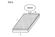
- the nano-polycrystalline diamond 1 of the present embodiment includes a group V element 3b formed on the substrate 2 and uniformly dispersed at the atomic level.
- V group element is dispersed at the atomic level means that carbon and a V group element are mixed in a gas phase state in a vacuum atmosphere to solidify solid carbon. When produced, it means a dispersion state at a level where the group V element is dispersed in the solid carbon.
- the nano-polycrystalline diamond 1 can be produced by subjecting graphite formed on a base material to a heat treatment.
- Graphite is an integral solid and includes a crystallized portion.
- the nanopolycrystalline diamond 1 has a flat plate shape, but it is conceivable to have an arbitrary shape and thickness.
- the nano-polycrystalline diamond 1 and the graphite basically have the same shape.
- the group V element can be added to the graphite at the stage of graphite formation. Specifically, a mixed gas of a gas containing a group V element and a hydrocarbon gas is pyrolyzed at a temperature of 1500 ° C. or more to form graphite on the substrate, and at the same time, the group V element is added to the graphite. Can do.
- the gas containing a group V element for example, a gas made of a hydride of a group V element can be used.
- An organometallic gas containing a group V element can also be used.
- phosphorus is added to graphite, one or more gases selected from trimethyl phosphorus, triethyl phosphorus, trimethyl phosphine, triphenyl phosphine, and tertiary butyl phosphine can be used.
- nitrogen is added to graphite, One or more gases selected from trimethylhydrazine and ammonia can be used.
- one or more gases selected from trimethylarsenic, triethylarsenic, and tertiarybutylarsine are used.
- one or more gases selected from trimethylantimony, triethylantimony, and tertiarybutylantimony can be used.
- bismuth to graphite Trimethyl bismuth, triethyl bismuth, tarsha rib It may be used one or more gases selected from Rubisumasu. It is also conceivable to appropriately mix two or more of the above gases.
- a group V element is mixed in a raw material gas for forming graphite in a gas phase, and the group V element is added to the graphite, so that the group V element is uniformly added to the graphite at the atomic level. can do. Further, by appropriately adjusting the addition amount of the gas containing the group V element to the hydrocarbon gas, a desired amount of the group V element can be added to the graphite.
- the thermal decomposition of the mixed gas can be carried out in a vacuum chamber, and at this time, by setting the degree of vacuum in the vacuum chamber to be relatively high, mixing of impurities into the graphite can be suppressed.
- unintended inevitable impurities are mixed in the graphite.
- the inevitable impurities include hydrogen, oxygen, boron, silicon, transition metals, and the like, and examples include elements other than the above group V elements.
- the amount of each inevitable impurity is about 0.01% by mass or less. That is, the concentration of inevitable impurities in graphite is about the detection limit or less in SIMS (Secondary Ion Mass Spectrometry) analysis. Moreover, about the transition metal, the density
- ICP Inductively Coupled Plasma
- the nano-polycrystalline diamond of the present embodiment contains a group V element uniformly at the atomic level as described above, but has a very small amount of impurities.
- atoms of group V elements do not agglomerate in a cluster shape in carbon, and are in a state of being almost uniformly dispersed throughout the entire diamond.
- the atoms of the group V element exist in an isolated state in the carbon.
- the atoms of group V elements are present in carbon (diamond body) in a state of substitution with carbon atoms, and are not simply mixed in the carbon, but the atoms of group V elements and carbon atoms are chemically bonded. It becomes the state that did.
- the nanopolycrystalline diamond of the present embodiment includes a group V element dispersed at an atomic level in carbon, a nanopolycrystalline diamond in which a group V element is uniformly added at an unprecedented level is provided. can get. Further, since the group V element can be uniformly dispersed at the atomic level in the nanopolycrystalline diamond, desired n-type conductivity can be imparted over the entire diamond. As a result, it is possible to impart excellent electron emission characteristics to diamond.
- a needle-shaped electron gun (electron emission source) having a shape that can be accommodated in a virtual cylindrical body having a thickness of 6 ⁇ m and a height of 25 ⁇ m was manufactured, and when the electron emission characteristics were investigated, this electron gun was found to be 5 kV. It has been found that an emission current of 150 ⁇ A can be steadily taken out by the extraction voltage, and can be used as a high-performance electron source.
- this electron gun is composed of nano-polycrystalline diamond, so it has no anisotropy and is excellent in durability.
- the needle breaks when a discharge occurs even once.
- the electron gun using nanopolycrystalline diamond according to the present embodiment does not break even after 5 to 10 discharges, and changes in characteristics after discharge are small. It turns out that there is a merit. Specifically, it was confirmed that the emission current was about 150 ⁇ A ⁇ 10 ⁇ A and that the change in the emission current was very small with an extraction voltage of 5 kV.
- the group V element-doped nanopolycrystalline diamond of the present embodiment for an electron gun, high-performance and stable electron emission characteristics can be realized while improving the durability of the electron gun.
- the group V element is dispersed in the diamond at the atomic level, so that the group V element mixed in the diamond in an aggregated state as described above. Almost does not exist. Further, the added group V element does not aggregate at the crystal grain boundary of diamond, and since there are very few impurities in diamond, the abnormal growth of the diamond crystal can be effectively suppressed. As a result, nano-polycrystalline diamond having a nano-sized crystal grain size (maximum crystal grain length) of 10 to 500 nm and n-type conductivity can be obtained.
- the concentration distribution of group V elements in the diamond is less likely to occur. Also from this, local abnormal growth of diamond crystal grains can be effectively suppressed. As a result, compared with the conventional example, the size of diamond crystal grains can be made uniform.
- the concentration of group V elements in diamond can be arbitrarily set.
- the concentration of the group V element in diamond can be increased or decreased.
- the group V element can be uniformly dispersed in the diamond, it is possible to effectively suppress the concentration distribution of the group V element in the diamond. Thereby, it is possible to effectively suppress the occurrence of variation in local conductivity of diamond.
- the addition concentration of the group V element is preferably in the range of about 10 14 to 10 22 / cm 3 in order to impart n-type conductivity to diamond.
- the addition concentration of the group V element is preferably about 10 19 / cm 3 or more, and in order to impart semiconductivity to diamond, the group V element The addition concentration of is preferably about 10 14 to less than 10 19 / cm 3 .
- the substrate is heated to a temperature of about 1500 ° C. to 3000 ° C. in a vacuum chamber.
- a well-known method can be adopted as the heating method.
- the base material any metal, inorganic ceramic material, or carbon material can be used as long as it can withstand a temperature of about 1500 ° C. to 3000 ° C.
- the base material is preferably made of carbon from the viewpoint of preventing impurities from being mixed into the raw material graphite. More preferably, it is conceivable that the base material is composed of diamond or graphite with very few impurities. In this case, at least the surface of the substrate may be composed of diamond or graphite.
- a hydrocarbon gas and a gas containing a group V element are introduced into the vacuum chamber.
- the degree of vacuum in the vacuum chamber is set to about 20 to 100 Torr.
- hydrocarbon gas and the gas containing a V group element can be mixed within a vacuum chamber.
- graphite in which a group V element is taken in at an atomic level can be formed on the substrate.
- the base material may be heated after the introduction of the mixed gas to form graphite containing a group V element on the base material.
- methane gas can be used as the hydrocarbon gas.
- the gas containing a group V element the various gases described above can be used.
- a mixed gas of a hydrocarbon gas and a gas containing a group V element can be introduced into the vacuum chamber at a ratio of 10 ⁇ 7 % to 100%, for example.
- a hydrocarbon gas and a gas containing a group V element flow toward the surface of the base material.
- each gas can be mixed efficiently in the vicinity of the substrate, and graphite containing a group V element can be efficiently generated on the substrate.
- the hydrocarbon gas or the group V element-containing gas may be supplied from directly above the base material toward the base material, or may be supplied toward the base material from an oblique direction or a horizontal direction. It is also conceivable to install a guide member that guides hydrocarbon gas or group V element-containing gas to the base material in the vacuum chamber.
- the crystal grain size in the crystallized portion of graphite is 10 ⁇ m or less as described above so that the crystal grain size of the diamond after conversion is on the order of nanometers.
- the crystal grain size of polycrystalline diamond can be about 10 to 500 nm.
- the step of converting graphite to diamond it is preferable to heat treat graphite in a high-temperature and high-pressure press without adding a sintering aid or catalyst. Further, in the step of converting graphite into diamond, the graphite formed on the base material may be subjected to heat treatment in a high-temperature high-pressure press.
- the graphite that can be used for producing the nano-polycrystalline diamond according to the present embodiment is, for example, crystalline or polycrystalline that partially includes a crystallized portion.
- the density of graphite is preferably greater than 0.8 g / cm 3 . Thereby, the volume change at the time of sintering graphite can be made small. Also, from the viewpoint of improving the yield by reducing the volume change when graphite is sintered, the density of graphite should be about 1.4 g / cm 3 or more and 2.0 g / cm 3 or less experimentally. Is more preferable.
- the density of the graphite is within the above range is that when the density of the graphite is lower than 1.4 g / cm 3 , the volume change during the high-temperature and high-pressure process is too large, and the temperature control may not be possible. It is possible. Moreover, if the density of graphite is larger than 2.0 g / cm 3 , the probability that diamond will crack may be doubled or more.
- Methane gas and trimethyl phosphorus were mixed at 1: 1 in a vacuum chamber, and the mixed gas was sprayed onto a diamond substrate heated to 1900 ° C. At this time, the degree of vacuum in the vacuum chamber was set to 20 to 30 Torr. As a result, graphite containing phosphorus was deposited on the substrate. The bulk density of this graphite was 2.0 g / cm 3 .
- the crystal grain size (maximum length of crystal grains) of graphite was about 100 nm to 10 ⁇ m. According to ICP elemental analysis, the phosphorus concentration in the graphite was 0.06%.
- the above graphite was converted to diamond at a synthesis temperature of 2200 ° C. and 15 GPa in a high-temperature and high-pressure press apparatus to obtain nano-polycrystalline diamond to which phosphorus was added.
- the crystal grain size of the polycrystalline diamond was 10 to 100 nm, respectively. From the X-ray pattern, no precipitation of phosphorus single phase was observed.
- This nanopolycrystalline diamond had a Knoop hardness of 120 GPa.
- a substrate having a size of 3 mm ⁇ 1 mm was cut out from the nano-polycrystalline diamond, and the electrical resistance of the substrate was measured to find 1 k ⁇ .
- Methane gas and trimethyl phosphate were mixed at a ratio of 1: 1 in a vacuum chamber, and the mixed gas was sprayed onto a diamond substrate heated to 1900 ° C. At this time, the degree of vacuum in the vacuum chamber was set to 20 to 30 Torr. As a result, graphite containing phosphorus was deposited on the substrate. The bulk density of this graphite was 2.0 g / cm 3 . In addition, according to SEM (Scanning Electron Microscope) observation, the crystal grain size of graphite was about 100 nm to 10 ⁇ m. According to ICP elemental analysis, the phosphorus concentration in the graphite was 0.5%.
- the above graphite was converted to diamond at a synthesis temperature of 2200 ° C. and 15 GPa in a high-temperature and high-pressure press apparatus to obtain nano-polycrystalline diamond to which phosphorus was added.
- the crystal grain size of the polycrystalline diamond was 10 to 100 nm, respectively. From the X-ray pattern, no precipitation of phosphorus single phase was observed.
- This nanopolycrystalline diamond had a Knoop hardness of 120 GPa.
- a substrate having a size of 3 mm ⁇ 1 mm was cut out from the nano-polycrystalline diamond, and the electric resistance of the substrate was measured.
- the electron emission characteristics of the nanopolycrystalline diamond of Example 19 were examined by the following method.
- a needle-shaped electron gun (electron emission source) having a shape that can be accommodated in a virtual cylindrical body having a thickness of 6 ⁇ m and a height of 25 ⁇ m was produced.
- This electron gun can constantly extract an emission current of 150 ⁇ A with an extraction voltage of 5 kV. Further, this electron gun did not break even after 5 to 10 discharges, and the electron emission characteristics after the discharge were stable with a very small change of 150 ⁇ A ⁇ 10 ⁇ A at an extraction voltage of 5 kV.
- the electrical resistance of the polycrystalline diamond was 800 k ⁇ .
- the degree of vacuum in the vacuum chamber is set to 20 to 30 Torr, and a hydrocarbon gas and a gas containing phosphorus are mixed in the vacuum chamber and heated to a temperature of about 1900 ° C.
- a hydrocarbon gas and a gas containing phosphorus are mixed in the vacuum chamber and heated to a temperature of about 1900 ° C.
Landscapes
- Chemical & Material Sciences (AREA)
- Organic Chemistry (AREA)
- Life Sciences & Earth Sciences (AREA)
- Inorganic Chemistry (AREA)
- Geology (AREA)
- General Life Sciences & Earth Sciences (AREA)
- Engineering & Computer Science (AREA)
- Ceramic Engineering (AREA)
- Chemical Kinetics & Catalysis (AREA)
- Structural Engineering (AREA)
- Materials Engineering (AREA)
- Manufacturing & Machinery (AREA)
- Carbon And Carbon Compounds (AREA)
- Crystals, And After-Treatments Of Crystals (AREA)
Abstract
L'invention porte sur du nanodiamant polycristallin (1) qui comporte du carbone, un élément étranger qui n'est pas du carbone (3) ajouté de façon à être dispersé dans tout le carbone à un niveau atomique et les impuretés inévitables. Ledit diamant polycristallin présente une taille des grains cristallins inférieure ou égale à 500 nm et peut être fabriqué en soumettant du graphite, auquel un élément étranger qui n'est pas du carbone a été ajouté de façon à être amené à être dispersé dans tout le carbone à un niveau atomique, à un traitement thermique dans un dispositif de type presse à haute pression.
Priority Applications (7)
| Application Number | Priority Date | Filing Date | Title |
|---|---|---|---|
| EP20204082.0A EP3805156A1 (fr) | 2011-07-28 | 2012-07-26 | Diamant polycristallin, son procédé de fabrication, outil de rainurage, mollette de rainurage, molette, outil rotatif, orifice de jet d'eau, filière de tréfilage, outil de coupe et source d'électrons |
| EP12818264.9A EP2738140B1 (fr) | 2011-07-28 | 2012-07-26 | Diamant polycristallin, son procédé de fabrication, outil de rainurage, mollette de rainurage, molette, outil rotatif, orifice de jet d'eau, filière de tréfilage, outil de coupe et source d'électrons |
| CN201280037943.0A CN103717530B (zh) | 2011-07-28 | 2012-07-26 | 多晶金刚石及其制法、划线工具、划线轮、修整器、旋转工具、水射流喷嘴、拉丝模具、切削工具、以及电子发射源 |
| US14/235,763 US9714197B2 (en) | 2011-07-28 | 2012-07-26 | Polycrystalline diamond and manufacturing method thereof, scribe tool, scribing wheel, dresser, rotating tool, orifice for water jet, wiredrawing die, cutting tool, and electron emission source |
| US15/163,298 US20160264422A1 (en) | 2011-07-28 | 2016-05-24 | Polycrystalline diamond and manufacturing method thereof, scribe tool, scribing wheel, dresser, rotating tool, orifice for water jet, wiredrawing die, cutting tool, and electron emission source |
| US15/167,315 US9878956B2 (en) | 2011-07-28 | 2016-05-27 | Polycrystalline diamond and manufacturing method thereof, scribe tool, scribing wheel, dresser, rotating tool, orifice for water jet, wiredrawing die, cutting tool, and electron emission source |
| US15/980,340 US10829379B2 (en) | 2011-07-28 | 2018-05-15 | Polycrystalline diamond and manufacturing method thereof, scribe tool, scribing wheel, dresser, rotating tool, orifice for water jet, wiredrawing die, cutting tool, and electron emission source |
Applications Claiming Priority (6)
| Application Number | Priority Date | Filing Date | Title |
|---|---|---|---|
| JP2011165749A JP5891639B2 (ja) | 2011-07-28 | 2011-07-28 | 多結晶ダイヤモンドおよびその製造方法、スクライブツール、スクライブホイール、ドレッサー、回転工具、ウォータージェット用オリフィス、伸線ダイス、ならびに切削工具 |
| JP2011165747A JP5891637B2 (ja) | 2011-07-28 | 2011-07-28 | 多結晶ダイヤモンドおよびその製造方法 |
| JP2011-165747 | 2011-07-28 | ||
| JP2011-165749 | 2011-07-28 | ||
| JP2011165748A JP5891638B2 (ja) | 2011-07-28 | 2011-07-28 | 多結晶ダイヤモンドおよびその製造方法ならびに電子放出源 |
| JP2011-165748 | 2011-07-28 |
Related Child Applications (3)
| Application Number | Title | Priority Date | Filing Date |
|---|---|---|---|
| US14/235,763 A-371-Of-International US9714197B2 (en) | 2011-07-28 | 2012-07-26 | Polycrystalline diamond and manufacturing method thereof, scribe tool, scribing wheel, dresser, rotating tool, orifice for water jet, wiredrawing die, cutting tool, and electron emission source |
| US15/163,298 Division US20160264422A1 (en) | 2011-07-28 | 2016-05-24 | Polycrystalline diamond and manufacturing method thereof, scribe tool, scribing wheel, dresser, rotating tool, orifice for water jet, wiredrawing die, cutting tool, and electron emission source |
| US15/167,315 Division US9878956B2 (en) | 2011-07-28 | 2016-05-27 | Polycrystalline diamond and manufacturing method thereof, scribe tool, scribing wheel, dresser, rotating tool, orifice for water jet, wiredrawing die, cutting tool, and electron emission source |
Publications (1)
| Publication Number | Publication Date |
|---|---|
| WO2013015348A1 true WO2013015348A1 (fr) | 2013-01-31 |
Family
ID=47601186
Family Applications (1)
| Application Number | Title | Priority Date | Filing Date |
|---|---|---|---|
| PCT/JP2012/068932 Ceased WO2013015348A1 (fr) | 2011-07-28 | 2012-07-26 | Diamant polycristallin, son procédé de fabrication, outil de rainurage, mollette de rainurage, molette, outil rotatif, orifice de jet d'eau, filière de tréfilage, outil de coupe et source d'électrons |
Country Status (4)
| Country | Link |
|---|---|
| US (4) | US9714197B2 (fr) |
| EP (2) | EP2738140B1 (fr) |
| CN (1) | CN103717530B (fr) |
| WO (1) | WO2013015348A1 (fr) |
Cited By (5)
| Publication number | Priority date | Publication date | Assignee | Title |
|---|---|---|---|---|
| JP2015030817A (ja) * | 2013-08-05 | 2015-02-16 | 住友電気工業株式会社 | 砥粒、研磨用スラリー、ワイヤーソー、結合体、工具および砥粒の製造方法 |
| WO2015184285A1 (fr) * | 2014-05-30 | 2015-12-03 | Baker Hughes Incorporated | Procédés de formation de diamant polycristallin et éléments de coupe et outils comprenant du diamant polycristallin |
| WO2018092364A1 (fr) * | 2016-11-16 | 2018-05-24 | 住友電工ハードメタル株式会社 | Procédé d'usinage de matériau à usiner, machine-outil, et procédé de fabrication d'élément, à l'aide d'un outil diamant équipé d'un diamant nanopolycristallin ou d'un diamant monocristallin synthétisé en phase vapeur |
| JPWO2021106075A1 (fr) * | 2019-11-26 | 2021-06-03 | ||
| WO2024239115A1 (fr) * | 2023-05-24 | 2024-11-28 | Morrow Corey | Méthode de fabrication d'un verre de montre |
Families Citing this family (11)
| Publication number | Priority date | Publication date | Assignee | Title |
|---|---|---|---|---|
| JP6007762B2 (ja) * | 2012-12-06 | 2016-10-12 | 住友電気工業株式会社 | ダイヤモンド多結晶体およびその製造方法、ならびに工具 |
| US20160161991A1 (en) * | 2014-12-08 | 2016-06-09 | Rubicon Technology, Inc. | Ultra-Thin, Passively Cooled Sapphire Windows |
| CN105561882A (zh) * | 2015-12-28 | 2016-05-11 | 河南广度超硬材料有限公司 | 一种多晶金刚石的制造方法 |
| US11761062B2 (en) | 2016-06-28 | 2023-09-19 | Schlumberger Technology Corporation | Polycrystalline diamond constructions |
| WO2018101346A1 (fr) * | 2016-11-30 | 2018-06-07 | 住友電気工業株式会社 | Diamant polycristallin ainsi que procédé de fabrication de celui-ci, outil de rainurage, roue de rainurage, dresseur, outil rotatif, filière à étirer, outil de coupe, électrode, et procédé d'usinage mettant en œuvre un diamant polycristallin |
| EP3549911B1 (fr) * | 2016-11-30 | 2022-06-01 | Sumitomo Electric Industries, Ltd. | Diamant polycristallin ainsi que procédé de fabrication de celui-ci, outil de coupe, et procédé d'usinage mettant en uvre un diamant polycristallin |
| WO2019077888A1 (fr) * | 2017-10-20 | 2019-04-25 | 住友電気工業株式会社 | Diamant monocristallin synthétique, outil, et procédé de production de diamant monocristallin synthétique |
| RU2680512C1 (ru) * | 2017-11-21 | 2019-02-21 | Федеральное государственное бюджетное учреждение науки Институт физики высоких давлений им. Л.Ф. Верещагина Российской академии наук (ИФВД РАН) | Способ получения наноразмерных алмазов |
| EP3834967A4 (fr) * | 2018-08-06 | 2022-05-04 | Sumitomo Electric Hardmetal Corp. | Outil de tournage |
| CN111304750A (zh) * | 2020-04-03 | 2020-06-19 | 湖州中芯半导体科技有限公司 | 一种提高cvd钻石硬度的方法 |
| US12186815B2 (en) | 2020-06-22 | 2025-01-07 | Sumitomo Electric Hardmetal Corp. | Cutting tool |
Citations (7)
| Publication number | Priority date | Publication date | Assignee | Title |
|---|---|---|---|---|
| JPH1045473A (ja) * | 1996-08-01 | 1998-02-17 | Toyo Tanso Kk | 耐酸化性に優れた熱分解炭素被覆黒鉛材 |
| JP2003292397A (ja) * | 2002-04-01 | 2003-10-15 | Techno Network Shikoku Co Ltd | ダイヤモンド多結晶体およびその製造方法 |
| WO2004104272A1 (fr) * | 2003-05-26 | 2004-12-02 | Sumitomo Electric Industries, Ltd. | Electrode a diamant et procede de production |
| JP2006045026A (ja) * | 2004-08-06 | 2006-02-16 | Sumitomo Electric Ind Ltd | 導電性ダイヤモンド被覆基板 |
| JP2009067609A (ja) * | 2007-09-11 | 2009-04-02 | Sumitomo Electric Ind Ltd | 高純度ダイヤモンド多結晶体およびその製造方法 |
| JP2010045184A (ja) * | 2008-08-12 | 2010-02-25 | Kobe Steel Ltd | 熱伝導性プレート部品及びこれを備えた電子部品 |
| JP2010222165A (ja) | 2009-03-23 | 2010-10-07 | Toyo Tanso Kk | ダイヤモンド薄膜を被覆した炭素材料及びその製造方法 |
Family Cites Families (2)
| Publication number | Priority date | Publication date | Assignee | Title |
|---|---|---|---|---|
| US5698328A (en) | 1994-04-06 | 1997-12-16 | The Regents Of The University Of California | Diamond thin film electron emitter |
| CN1735716A (zh) * | 2003-05-26 | 2006-02-15 | 住友电气工业株式会社 | 金刚石涂敷的电极及其制备方法 |
-
2012
- 2012-07-26 WO PCT/JP2012/068932 patent/WO2013015348A1/fr not_active Ceased
- 2012-07-26 EP EP12818264.9A patent/EP2738140B1/fr active Active
- 2012-07-26 US US14/235,763 patent/US9714197B2/en active Active
- 2012-07-26 CN CN201280037943.0A patent/CN103717530B/zh active Active
- 2012-07-26 EP EP20204082.0A patent/EP3805156A1/fr active Pending
-
2016
- 2016-05-24 US US15/163,298 patent/US20160264422A1/en not_active Abandoned
- 2016-05-27 US US15/167,315 patent/US9878956B2/en active Active
-
2018
- 2018-05-15 US US15/980,340 patent/US10829379B2/en active Active
Patent Citations (7)
| Publication number | Priority date | Publication date | Assignee | Title |
|---|---|---|---|---|
| JPH1045473A (ja) * | 1996-08-01 | 1998-02-17 | Toyo Tanso Kk | 耐酸化性に優れた熱分解炭素被覆黒鉛材 |
| JP2003292397A (ja) * | 2002-04-01 | 2003-10-15 | Techno Network Shikoku Co Ltd | ダイヤモンド多結晶体およびその製造方法 |
| WO2004104272A1 (fr) * | 2003-05-26 | 2004-12-02 | Sumitomo Electric Industries, Ltd. | Electrode a diamant et procede de production |
| JP2006045026A (ja) * | 2004-08-06 | 2006-02-16 | Sumitomo Electric Ind Ltd | 導電性ダイヤモンド被覆基板 |
| JP2009067609A (ja) * | 2007-09-11 | 2009-04-02 | Sumitomo Electric Ind Ltd | 高純度ダイヤモンド多結晶体およびその製造方法 |
| JP2010045184A (ja) * | 2008-08-12 | 2010-02-25 | Kobe Steel Ltd | 熱伝導性プレート部品及びこれを備えた電子部品 |
| JP2010222165A (ja) | 2009-03-23 | 2010-10-07 | Toyo Tanso Kk | ダイヤモンド薄膜を被覆した炭素材料及びその製造方法 |
Non-Patent Citations (1)
| Title |
|---|
| E. A. EKIMOV ET AL., NATURE, vol. 428, 2004, pages 542 - 545 |
Cited By (8)
| Publication number | Priority date | Publication date | Assignee | Title |
|---|---|---|---|---|
| JP2015030817A (ja) * | 2013-08-05 | 2015-02-16 | 住友電気工業株式会社 | 砥粒、研磨用スラリー、ワイヤーソー、結合体、工具および砥粒の製造方法 |
| WO2015184285A1 (fr) * | 2014-05-30 | 2015-12-03 | Baker Hughes Incorporated | Procédés de formation de diamant polycristallin et éléments de coupe et outils comprenant du diamant polycristallin |
| US9945185B2 (en) | 2014-05-30 | 2018-04-17 | Baker Hughes Incorporated | Methods of forming polycrystalline diamond |
| US10125551B2 (en) | 2014-05-30 | 2018-11-13 | Baker Hughes, A Ge Company, Llc | Cutting elements and earth-boring tools comprising polycrystalline diamond |
| WO2018092364A1 (fr) * | 2016-11-16 | 2018-05-24 | 住友電工ハードメタル株式会社 | Procédé d'usinage de matériau à usiner, machine-outil, et procédé de fabrication d'élément, à l'aide d'un outil diamant équipé d'un diamant nanopolycristallin ou d'un diamant monocristallin synthétisé en phase vapeur |
| JPWO2018092364A1 (ja) * | 2016-11-16 | 2019-10-10 | 住友電工ハードメタル株式会社 | ナノ多結晶ダイヤモンドまたは気相合成単結晶ダイヤモンドを備えるダイヤモンド工具を用いた、被加工材の加工方法、工作機械、及び、部材の製造方法 |
| JPWO2021106075A1 (fr) * | 2019-11-26 | 2021-06-03 | ||
| WO2024239115A1 (fr) * | 2023-05-24 | 2024-11-28 | Morrow Corey | Méthode de fabrication d'un verre de montre |
Also Published As
| Publication number | Publication date |
|---|---|
| CN103717530B (zh) | 2017-11-14 |
| US10829379B2 (en) | 2020-11-10 |
| US20160264422A1 (en) | 2016-09-15 |
| US20140186629A1 (en) | 2014-07-03 |
| US20160272546A1 (en) | 2016-09-22 |
| US9714197B2 (en) | 2017-07-25 |
| EP2738140A1 (fr) | 2014-06-04 |
| US9878956B2 (en) | 2018-01-30 |
| US20180257992A1 (en) | 2018-09-13 |
| EP2738140A4 (fr) | 2015-11-18 |
| EP3805156A1 (fr) | 2021-04-14 |
| EP2738140B1 (fr) | 2020-12-23 |
| CN103717530A (zh) | 2014-04-09 |
Similar Documents
| Publication | Publication Date | Title |
|---|---|---|
| WO2013015348A1 (fr) | Diamant polycristallin, son procédé de fabrication, outil de rainurage, mollette de rainurage, molette, outil rotatif, orifice de jet d'eau, filière de tréfilage, outil de coupe et source d'électrons | |
| JP5891639B2 (ja) | 多結晶ダイヤモンドおよびその製造方法、スクライブツール、スクライブホイール、ドレッサー、回転工具、ウォータージェット用オリフィス、伸線ダイス、ならびに切削工具 | |
| EP3549911B1 (fr) | Diamant polycristallin ainsi que procédé de fabrication de celui-ci, outil de coupe, et procédé d'usinage mettant en uvre un diamant polycristallin | |
| JP6752143B2 (ja) | 合成単結晶ダイヤモンド、合成単結晶ダイヤモンドの製造方法及び合成単結晶ダイヤモンドを用いた工具 | |
| CN109890753B (zh) | 多晶金刚石及其制法 | |
| JP6232817B2 (ja) | ナノ多結晶ダイヤモンドおよびこれを備える工具 | |
| JP2018203559A (ja) | 多結晶ダイヤモンドおよびその製造方法、スクライブツール、スクライブホイール、ドレッサー、回転工具、ウォータージェット用オリフィス、伸線ダイス、切削工具、電極ならびに多結晶ダイヤモンドを用いた加工方法 | |
| WO2021106075A1 (fr) | Outil de mesure ayant une partie pointe en diamant polycristallin | |
| JP2015030816A (ja) | 砥粒、研磨用スラリー、ワイヤーソー、結合体および砥粒の製造方法 | |
| JP5891638B2 (ja) | 多結晶ダイヤモンドおよびその製造方法ならびに電子放出源 | |
| JP2018197178A (ja) | 多結晶ダイヤモンドおよびその製造方法、スクライブツール、スクライブホイール、ドレッサー、回転工具、ウォータージェット用オリフィス、伸線ダイス、切削工具、電極ならびに多結晶ダイヤモンドを用いた加工方法 | |
| JP6743666B2 (ja) | 多結晶ダイヤモンドおよびその製造方法、スクライブツール、スクライブホイール、ドレッサー、回転工具、ウォータージェット用オリフィス、伸線ダイス、切削工具、電極ならびに多結晶ダイヤモンドを用いた加工方法 | |
| JP6349644B2 (ja) | 多結晶立方晶窒化ホウ素およびその製造方法 | |
| JP6194685B2 (ja) | 砥粒、研磨用スラリー、ワイヤーソー、結合体、工具および砥粒の製造方法 | |
| JP6307809B2 (ja) | ナノ多結晶ダイヤモンドおよびそれを備える工具 | |
| JP2018087117A (ja) | 多結晶ダイヤモンドおよびその製造方法、スクライブツール、スクライブホイール、ドレッサー、回転工具、伸線ダイス、切削工具、電極ならびに多結晶ダイヤモンドを用いた加工方法 | |
| JP6848361B2 (ja) | ダイヤモンドの研磨方法、ダイヤモンド切削工具の製造方法、およびダイヤモンドの製造方法 | |
| TW202239704A (zh) | 具有包含多晶鑽石之前端部之測定用工具 |
Legal Events
| Date | Code | Title | Description |
|---|---|---|---|
| 121 | Ep: the epo has been informed by wipo that ep was designated in this application |
Ref document number: 12818264 Country of ref document: EP Kind code of ref document: A1 |
|
| NENP | Non-entry into the national phase |
Ref country code: DE |
|
| WWE | Wipo information: entry into national phase |
Ref document number: 14235763 Country of ref document: US |
|
| WWE | Wipo information: entry into national phase |
Ref document number: 2012818264 Country of ref document: EP |