WO2013018176A1 - Dispositif d'éclairage - Google Patents
Dispositif d'éclairage Download PDFInfo
- Publication number
- WO2013018176A1 WO2013018176A1 PCT/JP2011/067528 JP2011067528W WO2013018176A1 WO 2013018176 A1 WO2013018176 A1 WO 2013018176A1 JP 2011067528 W JP2011067528 W JP 2011067528W WO 2013018176 A1 WO2013018176 A1 WO 2013018176A1
- Authority
- WO
- WIPO (PCT)
- Prior art keywords
- light emitting
- lamp
- substrate
- wiring pattern
- pipe
- Prior art date
- Legal status (The legal status is an assumption and is not a legal conclusion. Google has not performed a legal analysis and makes no representation as to the accuracy of the status listed.)
- Ceased
Links
Images





Classifications
-
- F—MECHANICAL ENGINEERING; LIGHTING; HEATING; WEAPONS; BLASTING
- F21—LIGHTING
- F21K—NON-ELECTRIC LIGHT SOURCES USING LUMINESCENCE; LIGHT SOURCES USING ELECTROCHEMILUMINESCENCE; LIGHT SOURCES USING CHARGES OF COMBUSTIBLE MATERIAL; LIGHT SOURCES USING SEMICONDUCTOR DEVICES AS LIGHT-GENERATING ELEMENTS; LIGHT SOURCES NOT OTHERWISE PROVIDED FOR
- F21K9/00—Light sources using semiconductor devices as light-generating elements, e.g. using light-emitting diodes [LED] or lasers
- F21K9/20—Light sources comprising attachment means
- F21K9/27—Retrofit light sources for lighting devices with two fittings for each light source, e.g. for substitution of fluorescent tubes
-
- H—ELECTRICITY
- H05—ELECTRIC TECHNIQUES NOT OTHERWISE PROVIDED FOR
- H05B—ELECTRIC HEATING; ELECTRIC LIGHT SOURCES NOT OTHERWISE PROVIDED FOR; CIRCUIT ARRANGEMENTS FOR ELECTRIC LIGHT SOURCES, IN GENERAL
- H05B45/00—Circuit arrangements for operating light-emitting diodes [LED]
-
- F—MECHANICAL ENGINEERING; LIGHTING; HEATING; WEAPONS; BLASTING
- F21—LIGHTING
- F21Y—INDEXING SCHEME ASSOCIATED WITH SUBCLASSES F21K, F21L, F21S and F21V, RELATING TO THE FORM OR THE KIND OF THE LIGHT SOURCES OR OF THE COLOUR OF THE LIGHT EMITTED
- F21Y2103/00—Elongate light sources, e.g. fluorescent tubes
- F21Y2103/10—Elongate light sources, e.g. fluorescent tubes comprising a linear array of point-like light-generating elements
-
- F—MECHANICAL ENGINEERING; LIGHTING; HEATING; WEAPONS; BLASTING
- F21—LIGHTING
- F21Y—INDEXING SCHEME ASSOCIATED WITH SUBCLASSES F21K, F21L, F21S and F21V, RELATING TO THE FORM OR THE KIND OF THE LIGHT SOURCES OR OF THE COLOUR OF THE LIGHT EMITTED
- F21Y2115/00—Light-generating elements of semiconductor light sources
- F21Y2115/10—Light-emitting diodes [LED]
-
- H—ELECTRICITY
- H10—SEMICONDUCTOR DEVICES; ELECTRIC SOLID-STATE DEVICES NOT OTHERWISE PROVIDED FOR
- H10H—INORGANIC LIGHT-EMITTING SEMICONDUCTOR DEVICES HAVING POTENTIAL BARRIERS
- H10H20/00—Individual inorganic light-emitting semiconductor devices having potential barriers, e.g. light-emitting diodes [LED]
- H10H20/80—Constructional details
- H10H20/85—Packages
- H10H20/857—Interconnections, e.g. lead-frames, bond wires or solder balls
-
- H—ELECTRICITY
- H10—SEMICONDUCTOR DEVICES; ELECTRIC SOLID-STATE DEVICES NOT OTHERWISE PROVIDED FOR
- H10W—GENERIC PACKAGES, INTERCONNECTIONS, CONNECTORS OR OTHER CONSTRUCTIONAL DETAILS OF DEVICES COVERED BY CLASS H10
- H10W90/00—Package configurations
Definitions
- Embodiments of the present invention relate to a lighting device including a lamp having a semiconductor light emitting element such as an LED (light emitting diode).
- a semiconductor light emitting element such as an LED (light emitting diode).
- LED light source for an illumination device having a plurality of LEDs.
- a wiring pattern is formed and a plurality of LED bare chips are mounted. Each LED chip is electrically connected to the wiring pattern by a bonding wire.
- a plurality of LED light sources are prepared, and their substrates are attached to a metal apparatus body.
- the device main body of the LED lighting device provided with such a light source is generally grounded.
- each LED chip of the light source emits light.
- the LED lighting device includes a straight tube type LED lamp having a base at both ends and sockets for supporting both ends of the lamp.
- the socket of this lighting device is generally a rotation mounting type.
- the LED lamp is attached to this socket in the following procedure. First, the lamp pin of the base is inserted from the tip of the socket, and the base of the base on which the lamp pin protrudes is disposed on the front side of the socket. Next, the LED lamp is rotated 90 degrees.
- the lamp pin is electrically connected to the terminal fitting disposed in the socket and mechanically supported.
- the straight tube fluorescent lamp attached to the lighting device in this manner emits light by being supplied with power through a socket that supports both ends or one of the sockets.
- the operation of attaching and detaching the LED lamp is preferable in that it does not differ from the conventional attachment and detachment operation of the straight tube type fluorescent lamp.
- the wiring pattern of the lamp is arranged close to the main body of the apparatus. For this reason, stray capacitance may occur between the grounded metal device body and the wiring pattern. It has been confirmed that the size of the stray capacitance increases as the area of the wiring pattern forming the electrode for this capacitance increases.
- the present inventors have found a phenomenon in which a straight tube type LED lamp is lit darkly due to this stray capacitance.
- the device body at the ground potential is one electrode, and the wiring pattern is the other electrode.
- each LED chip emits light erroneously.
- Such erroneous light emission is called dark lighting.
- the dark lighting is noticeable when the power is turned off in a dark environment. Therefore, in developing an illuminating device that supports a straight tube type LED lamp, it is required not to emit the dark light as described above.
- Embodiment is providing the illuminating device which can prevent the dark lighting in the state in which the power supply was turned off.
- a straight tube lamp supported by the first and second sockets includes a long pipe made of translucent resin material, a light emitting module accommodated in the pipe, and a pipe A first cap attached to one end and a second cap attached to the other end of the pipe are provided.
- a wiring pattern having a mounting pad and a conductive connection portion is formed on the substrate of the light emitting module.
- a semiconductor light emitting element having a pair of electrodes is fixed on each mounting pad. One electrode is electrically connected to the conductive connection portion. The other electrode and the mounting pad are electrically connected.
- the first base has two lamp pins electrically connected to the wiring pattern.
- the second base is made non-conductive with the wiring pattern.
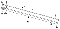
- FIG. 1 is a perspective view illustrating the lighting apparatus according to the first embodiment.
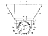
- FIG. 2 is a cross-sectional view showing the lighting apparatus of FIG.
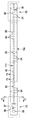
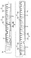
- FIG. 3 is a front view showing a state in which a plurality of light emitting modules included in the lamp of the lighting fixture of FIG. 1 are arranged.
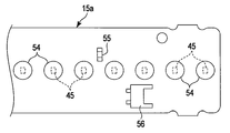
- FIG. 4 is a front view showing one of the light emitting modules of FIG.
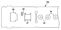
- FIG. 5 is an enlarged front view showing a portion F5 in FIG. 6 is an enlarged front view showing the F6 portion in FIG. 7 is a cross-sectional view taken along line F7-F7 in FIG.
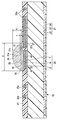
- FIG. 8 is a cross-sectional view taken along line F8-F8 in FIG.
- FIG. 9 is a front view showing the light emitting module of FIG.
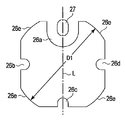
- FIG. 10 is an enlarged view of a portion F10 in FIG.
- FIG. 11 is an enlarged view showing a part of F11 in FIG.
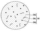
- FIG. 12 is a schematic diagram illustrating a configuration of a sealing member included in the light emitting module of FIG. 4.
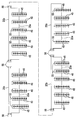
- FIG. 13 is a front view showing a wiring pattern of the light emitting module of FIG.
- FIG. 14 is a diagram showing an electric circuit of a lamp provided in the lighting fixture of FIG.
- FIG. 15 is a connection diagram of the lighting fixture of FIG.
- the lighting device of Embodiment 1 includes a device main body provided in a non-grounded state; a lighting device that outputs direct current: a first socket that is attached to the device main body and is supplied with the output of the lighting device; and the lighting device.
- a second socket attached to the apparatus body in a non-conductive state and paired with the first socket; a straight tube lamp removably supported by the first and second sockets; The lamp has the following configuration.
- the lamp includes a pipe formed in a long shape by a light-transmitting material having electrical insulation; a substrate formed long in a direction in which the pipe extends, and a mounting pad arranged in the longitudinal direction of the substrate; A wiring pattern having a plurality of conductive connection portions is formed on the substrate, a semiconductor light emitting element having a pair of electrodes is fixed on each mounting pad, and one electrode and the conductive connection portion are electrically connected.
- a light emitting module formed by electrically connecting the other electrode and the mounting pad and housed in the pipe; and having two lamp pins electrically connected to the wiring pattern
- a first base attached to one end in the longitudinal direction of the pipe and supported by the first socket; and having a lamp pin and being non-conductive with the wiring pattern at the other end in the longitudinal direction of the pipe
- Comprises attached to, a second cap is supported on the second socket.
- a polycarbonate resin can be suitably used as the translucent material forming the pipe.
- This pipe is preferably formed by mixing an appropriate amount of a light diffusing material with a resin material.
- a single-layer or multi-layer resin substrate, a ceramic substrate, or the like can be used as the substrate.
- a metal foil such as aluminum, iron, or copper is laminated on the back surface. Thereby, it is possible to suppress the warpage of the substrate and improve the heat dissipation from the substrate.
- the semiconductor light-emitting element can typically be an LED (light-emitting diode) chip, but a semiconductor laser can also be used, and an EL (electroluminescence) element can also be used. Is possible.
- the emission color may be any of red, green, and blue. It is also possible to use a combination of LED chips of different emission colors.
- the electrical connection between the electrode of the light emitting element and the conductive connection portion can be performed using, for example, a wire, but is not limited thereto.
- the electrical connection between the electrode of the light emitting element and the mounting pad can also be performed using a wire, but this is not restrictive.
- a back electrode in which the light emitting element is connected to the terminal is used. When it has, it may be responsible for electrical connection by adhering the back electrode to the mounting pad.
- the first and second sockets are used in conformity with the shape of the lamp pins of the first and second caps. For example, if the lamp pin of the base is bent in an L shape, it is desirable to use a socket that matches that.
- the apparatus main body is not grounded, and the second socket is not electrically connected to the lighting device.
- the light emitting module is electrically insulated by a pipe that accommodates the light emitting module.
- the wiring pattern of the light emitting module is electrically connected only to the lamp pin provided in the first base on the power supply side, and is not electrically connected to the lamp pin provided in the second base.
- the lamp is not grounded while being supported by the first and second sockets of the apparatus main body.
- stray capacitance does not occur between the apparatus main body and the wiring pattern of the light emitting module in the pipe. Therefore, when the lamp is turned off, dark lighting of the lamp due to stray capacitance is prevented.
- the substrate of the light emitting module is separated from the metal portion of the second base at a distance that the potential of the lamp pin of the second base does not reach the wiring pattern in Embodiment 1. .
- external noise may be superimposed on the lamp pin of the second base that is mechanically supported without being electrically connected to the second socket in the first embodiment. In this case, since external noise is prevented from spreading from the second base to the wiring pattern of the light emitting module, the light emitting operation of the light emitting module is properly maintained.
- the wiring pattern according to Embodiment 1 has a plurality of pattern portions, and these pattern portions are formed by a mounting region and a conductive region integrally extending from the mounting region.
- a mounting region and a conductive region of the pattern portion adjacent to the substrate are aligned in the width direction of the substrate, and the mounting region extends in the longitudinal direction of the substrate and is formed in a size that allows a plurality of the mounting pads to be provided.
- the conductive region has a plurality of the conductive connection portions, and the plurality of light emitting elements and the mounting pads and the conductive portions of the pattern portions adjacent to each other through the first and second wires connected thereto are electrically connected.
- the connecting part is electrically connected.
- a plurality of light emitting elements are mounted in the mounting regions of the respective pattern portions of the wiring pattern, and these light emitting elements are electrically connected in parallel.
- the pattern portions adjacent in the longitudinal direction of the substrate are electrically connected in series. For this reason, each light emitting element can be light-emitted simultaneously by the electric power feeding through a 1st nozzle
- a capacitor is mounted on the substrate in Embodiment 3, and the capacitor is electrically connected in parallel to the plurality of light emitting elements disposed in the mounting area.
- the noise when noise is superimposed on the wiring pattern after the lamp is turned off, the noise bypasses the light emitting element and flows to the capacitor. Thereby, it is possible to expect an effect that it is possible to prevent erroneous lighting in a state where the power is turned off.
- reference numeral 1 exemplifies a direct-mounted one-lamp lighting fixture.
- the luminaire 1 includes an apparatus main body (apparatus main body) 2, a lighting device 3, sockets 4a and 4b that make a pair, a reflecting member 5, a straight tube lamp 11 that forms a light source, and the like.
- the apparatus main body 2 is made of, for example, an elongated metal plate.
- the apparatus main body 2 extends in the front and back direction of the paper surface depicting FIG.
- the apparatus main body 2 is fixed to, for example, an indoor ceiling using a plurality of screws (not shown).
- the lighting device 3 is fixed to the middle portion of the device body 2 in the longitudinal direction.
- the lighting device 3 is configured to receive a commercial AC power supply and generate a DC output, and supplies the DC output to a lamp 11 described later.
- a power terminal block (not shown), a plurality of member support brackets, a pair of socket support members, and the like are attached to the apparatus main body 2.
- the power supply terminal block is connected with a power line of commercial AC power drawn from behind the ceiling. Furthermore, the power terminal block is electrically connected to the lighting device 3 via an in-appliance wiring (not shown).
- the sockets 4a and 4b are connected to the socket support member and disposed at both ends in the longitudinal direction of the apparatus main body 2, respectively.
- the sockets 4a and 4b are of a rotational mounting type. These sockets 4a and 4b are dedicated sockets suitable for bases 13a and 13b provided in the lamp 11 described later.
- the sockets 4a and 4b are provided with a pair of terminal fittings 8 or 9 to which lamp pins 16a and 16b described later are connected.
- the terminal fitting 8 of the socket 4a on one side is connected to the lighting device 3 via the in-apparatus wiring as shown in FIG. No wiring is connected to the terminal fitting 9 of the other socket 4b.
- the reflecting member 5 has, for example, a metal bottom plate portion 5a, a side plate portion 5b, and an end plate 5c, and has a trough shape with an open upper surface.
- the bottom plate portion 5a is flat.
- the side plate portion 5b is bent obliquely upward from both ends in the width direction of the bottom plate portion 5a.
- the end plate 5c closes the end surface opening formed by the longitudinal ends of the bottom plate portion 5a and the side plate portion 5b.
- the metal plate that forms the bottom plate portion 5a and the side plate portion 5b is made of a color steel plate whose surface exhibits a white color. For this reason, the surface of the baseplate part 5a and the side plate part 5b is a reflective surface.
- socket through holes are opened at both longitudinal ends of the bottom plate portion 5a.
- the reflection member 5 covers the device main body 2 and each component attached thereto. This state is held by a removable decorative screw 6 (see FIG. 1).
- the decorative screw 6 penetrates the bottom plate portion 5a upward and is screwed into the member support fitting. This decorative screw 6 can be manually operated without using a tool.
- the sockets 4a and 4b protrude through the socket through holes to the lower side of the bottom plate portion 5a.
- the lighting fixture 1 is not limited to one lamp, and can be implemented as a two-lamp lighting fixture that includes two pairs of sockets and can support two lamps 11 described below.
- the lamp 11 detachably supported by the sockets 4a and 4b will be described below with reference to FIGS.
- the lamp 11 has the same dimensions and outer diameter as the existing fluorescent lamp.
- the lamp 11 includes a pipe 12, first and second caps 13 a and 13 b attached to both ends of the pipe 12, a beam 14, and at least one, for example, four light emitting modules 15. In the case of distinguishing the four light emitting modules 15, the subscripts a to d are attached and illustrated and described.
- the pipe 12 is formed in a long shape with a translucent resin material.
- a resin material forming the pipe 12 a polycarbonate resin mixed with a light diffusing material can be suitably used.
- the diffuse transmittance of the pipe 12 is preferably 90% to 95%.
- the pipe 12 has a pair of convex parts 12a on the inner surface of the upper part in its use state.
- the first base 13 a is attached to one end of the pipe 12 in the longitudinal direction
- the second base 13 b is attached to the other end in the longitudinal direction of the pipe 12.
- These first and second caps 13a and 13b are detachably connected to the sockets 4a and 4b.
- the lamp 11 supported by the sockets 4 a and 4 b by this connection is disposed immediately below the bottom plate portion 5 a of the reflecting member 5. A part of the light emitted from the lamp 11 to the outside enters the side plate portion 5 b of the reflecting member 5.
- the first base 13a has two lamp pins 16a protruding to the outside. These lamp pins 16a are electrically insulated from each other. At the same time, the tip portions of the two lamp pins 16a are bent at a substantially right angle so as to be separated from each other and have an L shape.
- the second base 13b has a single lamp pin 16b projecting to the outside.
- the lamp pin 16b has a cylindrical shaft portion and a front end portion (not shown) which is provided at the front end and has an elliptical shape or an oval shape, and has a side T shape.
- the lamp pin 16a of the first base 13a is connected to the terminal fitting 8 of the socket 4a, and the lamp pin 16b of the second base 13b is connected to the terminal fitting 9 of the socket 4b, whereby the lamp 11 is connected to the sockets 4a and 4b.
- Mechanically supported In this supported state, power can be supplied to the lamp 11 by the terminal fitting 8 in the first socket 4a and the lamp pin 16a of the first base 13a in contact therewith.
- the beam 14 is accommodated in the pipe 12.
- the beam 14 is a bar material having excellent mechanical strength, and is formed of, for example, an aluminum alloy for weight reduction. Both longitudinal ends of the beam 14 are electrically insulated and connected to the caps 13a and 13b.
- the beam 14 has, for example, a plurality of substrate support portions 14a each having a rib shape (only one is shown in FIG. 2).
- the four light emitting modules 15a to 15d are all formed in a long and narrow rectangle, and are arranged in a straight line.
- the length of this module row is substantially equal to the total length of the beam 14.
- the light emitting modules 15a to 15d are fixed by screws (not shown) that are screwed into the beam 14 through the light emitting modules 15a to 15d.
- the light emitting modules 15a to 15d are accommodated in the pipe 12 together with the beam 14. In this supported state, both ends in the width direction of the light emitting modules 15a to 15d are placed on the convex portions 12a of the pipe 12. Accordingly, the light emitting modules 15a to 15d are disposed substantially horizontally above the maximum width portion in the pipe 12.
- Each light emitting module 15 includes a substrate 21, a wiring pattern 25, a protection member 41, a plurality of light emitting elements 45, a first wire 51, a second wire 52, a sealing member 54, and various electrical components 55. To 59.
- the substrate 21 has a base 22, a metal foil 23, and a cover layer 24.
- the base 22 is made of a flat plate made of resin such as glass epoxy resin.
- This glass epoxy resin substrate (FR-4) has a low thermal conductivity and is relatively inexpensive.
- the base 22 may be formed of a glass composite substrate (CEM-3) or other synthetic resin material.
- the metal foil 23 is laminated on the back surface of the substrate 21 and is made of, for example, copper foil.
- the cover layer 24 is laminated over the metal foil 23 and the back surface of the peripheral portion of the base 22.
- the cover layer 24 is made of a resist layer made of an insulating material such as synthetic resin.
- the substrate 21 is reinforced by the metal foil 23 and the cover layer 24 laminated on the back surface thereof so as not to warp.
- the wiring pattern 25 has a three-layer structure as shown in FIGS. 7 and 8 and is formed on the surface of the base 22 (that is, the surface of the substrate 21).
- the first layer U is formed of copper plated on the surface of the base 22.
- the second layer M is plated on the first layer U and is formed of nickel.
- the third layer T is plated on the second layer M and is made of silver.
- the surface of the wiring pattern 25 is made of silver.
- the silver third layer T forms a reflecting surface, and the total light reflectance thereof is 90% or more.
- FIG. 13 shows in detail the wiring pattern 25 formed on the substrate 21 of the light emitting module 15a.
- a first wiring pattern 25a and a second wiring pattern 25b are provided.
- the first wiring pattern 25 a has a plurality of pattern portions 31 arranged in the longitudinal direction of the substrate 21. Each pattern portion 31 is formed by a mounting region 31a and a conductive region 31b.
- the mounting region 31 a extends in the longitudinal direction of the substrate 21, and is formed in such a size that a plurality of mounting pads 26 described later are arranged in the longitudinal direction of the substrate 21. For this reason, the width
- the conductive region 31b is integrally extended from the mounting region 31a.
- the conductive region 31b has a portion along an edge extending in the longitudinal direction of the substrate 21 and a plurality of branch portions branched substantially perpendicularly from this portion. The leading end of each branch portion forms a conductive connecting portion 27 described later.
- the mounting region 31 a of one pattern portion 31 and the conductive region 31 b of the other pattern portion 31 are arranged in a pair in the thickness direction of the substrate 21. ing.
- the number of the branch portions is the same as the number of mounting pads 26 to be described later formed in the mounting region 31a paired with the conductive region 31b having the branch portion.
- the configuration of the wiring pattern formed on the substrate 21 of the other light emitting modules 15b to 15c is the same as the wiring pattern 25 of the light emitting module 15a described above although not shown. Therefore, redundant description is omitted.
- the substrate 21 of the light emitting module 15d closest to the second base 4b is separated from the metal portion of the second base 4b by a predetermined distance. This distance is approximately 6 mm, for example. Such a separation distance prevents the potential due to the external noise superimposed on the lamp pin 16b of the second cap 4b from reaching the wiring pattern 25 formed on the substrate 21 of the light emitting module 15d. Thereby, the light emission operation
- a white resist layer mainly composed of an electrically insulating synthetic resin can be suitably used.
- This white resist layer functions as a reflective layer having a high light reflectance.
- the protection member 41 is formed on the substrate 21 so as to cover most of the wiring pattern 25.
- the protection member 41 covers the wiring pattern 25 while leaving a plurality of positions of the second wiring pattern 25 b among the wiring patterns 25 as mounting pads 26. At the same time, the protection member 41 covers the wiring pattern 25 while leaving the leading end portions of the plurality of branches included in the first wiring pattern 25 a among the wiring patterns 25 as the conductive connection portions 27. Furthermore, the protection member 41 covers the wiring pattern 25 except for mounting locations for electrical components 55 to 59 described later.
- Each mounting pad 26 and each conductive connection portion 27 are formed in a portion where the third layer T is exposed without being covered with the protective member 41 when the protective member 41 is formed on the substrate 21. As shown in FIG. 9, the mounting pads 26 are arranged in the longitudinal direction of the substrate 21. Each conductive connection portion 27 is arranged in the vicinity of each mounting pad 26 in a pair with each mounting pad 26. Therefore, the respective conductive connection portions 27 are arranged in the longitudinal direction of the substrate 21 at the same arrangement pitch as that of the mounting pads 26.
- the mounting pad 26 has grooves 26a to 26d in at least one place, for example, four places in the periphery.
- the grooves 26a to 26b are separated from each other by 90 degrees.
- the depths of the grooves 26a to 26b are 1/10 to 1/5 of the pad diameter D1, which will be described later.
- the peripheral edge of the mounting pad 26 has an edge portion 26e having an arc shape every 90 degrees. Each edge portion 26e is formed between the grooves 26a to 26d adjacent to each other in the circumferential direction of the mounting pad 26.
- the mounting pad 26 Since the mounting pad 26 has the grooves 26a to 26b and the edge 26e, the mounting pad 26 has a substantially clover shape.
- the groove 26a is larger than the other three grooves 26b to 26d, and the conductive connection portion 27 is disposed inside thereof.
- the mounting pad 26 is formed symmetrically with respect to a straight line L (shown by a one-dot chain line in FIG. 10) passing through the center and the conductive connection portion 27.
- the mounting pad 26 having a substantially clover shape and the conductive connection portion 27 provided in the groove 26a can contribute to reducing the diameter D of the sealing member 54 described later.
- the pad diameter D1 of the mounting pad 26 is, for example, 3.6 mm.
- the pad diameter D1 is a dimension between the edge portions 26e positioned in pairs with the center of the mounting pad 26 as a boundary.
- the protective member 41 is filled in each of the grooves 26a to 26b.
- the portion of the protection member 41 filled in the grooves 26a to 26b is referred to as a filling portion 42 (see FIGS. 7 and 11).
- Each filling portion 42 forms a convex portion that protrudes toward the center of the mounting pad 26.
- These filling portions 42 protrude from the surface of the third layer T in the stacking direction of the wiring pattern 25 (see FIG. 7).
- At least one of the filling portions 42 is used as a reference for determining the mounting position when a light emitting element 45 described later is mounted on the mounting pad 26.
- the filling portion 42 for the groove 26 a is filled in the groove 26 a avoiding the conductive connection portion 27.
- the plurality of light emitting elements 45 are LED bare chips.
- an LED bare chip that emits blue light is used as the bare chip.
- An LED bare chip has a light emitting layer on one surface of an element substrate made of sapphire and has a rectangular planar shape.
- an electrode 45b forming an anode and an electrode 45a forming a cathode are provided in the light emitting layer side by side, for example, in the longitudinal direction of an LED bare chip.
- These light emitting elements 45 have the other surface of the element substrate opposite to the one surface fixed to a mounting pad 26 which is a reflective surface using an adhesive 46 (see FIGS. 7 and 8).
- each light emitting element 45 is bonded on the mounting pad 26 such that the alignment of the electrodes 45 a and 45 b is aligned with the grooves 26 a and 26 c of the mounting pad 26.
- the light emitting elements 45 thus mounted on the mounting pads 26 form a light emitting element array arranged in the longitudinal direction of the substrate 21 (the direction in which the central axis extends). In this row, the arrangement pitch of the light emitting elements 45 is 5 mm or more and 9 mm below.
- the bonding portion of the light emitting element 45 is the central portion of the mounting pad 26. As a result, the light emitted from the light emitting element 45 and incident on the mounting pad 26 can be reflected in the reflective surface area around the light emitting element 45.
- the light incident on the mounting pad 26 becomes stronger as it approaches the light emitting element 45, and this strong light can be reflected by the reflection surface region.
- the grooves 26a to 26d are out of the reflective surface area that reflects the strong light. Therefore, the area of the surface (reflection surface) of the mounting pad 26 is reduced by the grooves 26 a to 26 d in the peripheral portion of the mounting pad 26. However, this does not substantially reduce the reflection performance of the mounting pad 26 and can be ignored.
- the light emitting element 45 Since light emission of the light emitting element 45 composed of a bare LED chip is realized by passing a forward current through a pn junction of a semiconductor, the light emitting element 45 is a solid element that directly converts electric energy into light.
- the light emitting element 45 that emits light by such a light emission principle has an energy saving effect as compared with an incandescent bulb that incandescents a filament to a high temperature by energization and emits visible light by its thermal radiation.
- the adhesive 46 preferably has heat resistance in order to obtain adhesion durability, and further has translucency so that reflection can be performed directly under the light emitting element 45.
- a silicone resin adhesive can be suitably used as such an adhesive 46.
- the first wire 51 and the second wire 52 are an example of conductive means. These wires are made of fine metal wires such as gold fine wires, and are wired using a bonding machine.
- the first wire 51 is provided by electrically connecting the light emitting element 45 and the conductive connection portion 27 of the first wiring pattern 25a.
- one end 51 a of the first wire 51 is connected to the electrode 45 a of the light emitting element 45 by first bonding.
- the other end portion 51 b of the first wire 51 is connected to the conductive connection portion 27 by the second bonding.
- One end 51 a of the first wire 51 protrudes in the direction away from the light emitting element 45 in the thickness direction of the light emitting element 45.
- the conductive connection portion 27 is closer to the substrate 21 than the electrodes 45 a and 45 b of the light emitting element 45 with respect to the thickness direction of the light emitting element 45.
- the other end portion 51 b of the first wire 51 is connected to the conductive connection portion 27 at an angle.
- the intermediate part 51c of the first wire 51 is a part occupying between the one end part 51a and the other end part 51b. As shown in FIG. 7, the intermediate portion 51 c is formed so as to bend from the one end portion 51 a and be parallel to the light emitting element 45.
- the protrusion height h of the intermediate portion 51c with respect to the light emitting element 45 is defined as 75 ⁇ m or more and 125 ⁇ m or less, preferably 60 ⁇ m or more and 100 ⁇ m or less.
- the intermediate portion 51 c of the first wire 51 is bent from the one end portion 51 a so as to be parallel to the light emitting element 45 includes that the intermediate portion 51 c is parallel to the light emitting element 45. .
- the intermediate portion 51 c may not be completely parallel to the light emitting element 45 due to manufacturing variations. Such variations are also included in the scope of the phrase “to be parallel”.
- the intermediate portion 51 c of the first wire 51 is substantially parallel to the light emitting element 45. Therefore, an aspect in which the intermediate portion 51c of the first wire 51 is obliquely bent from the one end portion 51a and the angle between the one end portion 51a and the intermediate portion 51c is an acute angle is out of the scope of the wording. It is.
- the intermediate portion 51c and the other end portion 51b of the first wire 51 wired as described above extend in a direction orthogonal to the direction in which the light emitting elements 45 form a row.
- Such wiring is realized by the above-described arrangement of the light emitting element 45 with respect to the mounting pad 26. With this wiring, the length of the first wire 51 can be shortened. For this reason, the cost of the 1st wire 51 can be reduced compared with the case where the 1st wire 51 is wired diagonally with respect to a light emitting element in planar view.
- the second wire 52 is provided by connecting the light emitting element 45 and the mounting pad 26 formed of a part of the first wiring pattern 25a by wire bonding.
- one end of the second wire 52 is connected to the electrode 45b of the light emitting element 45 by first bonding.
- the other end of the second wire 52 is connected to the mounting pad 26 by second bonding.
- the plurality of light emitting elements 45 mounted on the mounting region 31a of each pattern unit 31 are electrically connected in parallel to each other, and these light emitting element groups connected in parallel are electrically connected in series. Yes.
- This circuit configuration is shown in FIG.
- the light emitting elements 45 can emit light all at once by feeding through the first cap 13a. At the same time, when the first wire 51 and the second wire 52 are disconnected due to, for example, a bonding failure, even if the power supply to one light emitting element 45 is stopped, the entire lamp 11 is connected by the parallel connection. Does not stop flashing.
- the sealing member 54 is formed by mixing an appropriate amount of a phosphor 54b and a filler 54c with a resin 54a as a main component, as schematically shown in FIG.
- the resin 54a may be any thermoplastic resin having translucency.
- a resin silicone resin is preferably used for the resin 54a. Since the resin-based silicone resin has a three-dimensionally crosslinked structure, the phosphor 54b that is harder than the translucent silicone rubber is excited by the light emitted from the light emitting element 45, and the light emitting element 45 emits. It emits light of a color different from the color of light. In Example 1, since the light emitting element 45 emits blue light, a yellow phosphor that emits yellow light having a complementary color relationship to the blue light by the excitation is used. Thereby, white light can be emitted as output light of the lamp 11 which is a light emitting device.
- the sealing member 54 is formed on the substrate 21 by sealing the mounting pad 26, the conductive connection portion 27, the light emitting element 45, the first wire 51, and the second wire 52.
- the sealing member 54 is formed by being dripped over the light emitting element 45 in an uncured state, and then cured by heat treatment.
- a dispenser or the like is used for dropping (potting) the sealing member 54.
- the cured sealing members 54 are arranged on the substrate 21 at predetermined intervals in the longitudinal direction of the substrate 21, and are arranged in a sealing member row according to the row of the light emitting elements 45.
- the cured sealing member 54 is bonded onto the substrate 21 and rises from the bonded bottom surface to form a dome shape or Mt. Fuji shape.
- the diameter D (see FIG. 7) of the sealing member 54 is defined as 1.0 to 1.4 times the pad diameter D1, and in the case of Example 1, the diameter D is 4.0 mm to 5.0 mm. Thereby, a part of the mounting pad 26 does not protrude from the sealing member 54. At the same time, the number of sealing members 54 is not excessive with respect to the mounting pad 26, and the amount of the sealing member 54 used can be made appropriate while maintaining the aspect ratio described later. There is no frame or the like surrounding the light emitting element 45 or the like in order to define the height H and the diameter D of the sealing member 54 from the bottom surface. Therefore, the diameter D and height H of the sealing member 54 are controlled by the amount of dripping of the sealing member 54, the hardness, and the time until it is cured.
- the raised height H of the sealing member 54 with respect to the light emitting element 45 is 1.0 mm or more.
- the aspect ratio of the sealing member 54 is set to 0.22 to 1.00.
- the aspect ratio of the sealing member 54 is a ratio (H / D) of the diameter D of the sealing member 54 to the height H of the rising of the sealing member 54 with respect to the light emitting element 45.
- the ratio of the orthogonal diameters of the sealing member 54 is 0.55 to 1.00.
- the ratio of the orthogonal diameters refers to the ratio of the diameters X and Y orthogonal to each other on the bottom surface of the sealing member 54 bonded to the substrate 21 as shown in FIG.
- the diameter X is a diameter of the bottom surface arbitrarily drawn through the center of the light emitting element 45.
- the diameter Y is the diameter of the bottom surface drawn perpendicular to the diameter X.
- the electrical component 55 shown in any of FIGS. 4 to 6 is a capacitor.
- the electrical component 56 is a connector.
- the electrical component 57 is a rectifying diode.
- the electrical component 58 is a resistor.
- the electrical component 59 is an input connector.
- the electrical component 55 made of a capacitor is mounted on each of the four light emitting modules 15.
- the capacitor is electrically connected in parallel to each of the light emitting element groups connected in parallel on the mounting region 31a of the first wiring pattern 25a as shown in FIG.
- the electrical component 55 arranged in this manner functions as a bypass element that bypasses the noise superimposed on the wiring pattern 25 of each light emitting module 15 to the light emitting element group. Thereby, the superimposition of noise on the light emitting element group is suppressed. Accordingly, it is possible to prevent the lamp 11 from being erroneously turned on due to noise flowing into the light emitting element 45 in a state where the power is turned off by the switch SW shown in FIG.
- the electrical component 56 formed of a connector has light-emitting modules 15 a and 15 d disposed at both ends in the longitudinal direction of the light-emitting module row formed by the four light-emitting modules 15. Has been implemented. Furthermore, the electrical components 56 are mounted on both ends in the longitudinal direction of the light emitting modules 15b and 15c disposed between the light emitting modules 15a and 15d, respectively. These electrical components 56 are connected to the terminal portion of the first wiring pattern 25a and the terminal portion of the second wiring pattern 25b (see FIG. 14).
- the electrical components 56 of the adjacent light emitting modules 15 are connected to each other by an unillustrated electric wire. With such connection, the light emitting modules 15 are electrically connected in series.
- the electrical components 57 to 59 are all mounted on the other end of the light emitting module 15a.
- An electrical component 59 composed of an input connector is connected to the wiring pattern 25 of the light emitting module 15a. Electric wires (not shown) connected to the electrical component 59 are respectively connected to the lamp pins 16a of the first base 13a disposed closer to the electrical component 59.
- the straight tube lamp 11 having the above-described configuration has a configuration in which the light emitting module 15 is electrically insulated by a pipe 12 that accommodates the light emitting module 15. At the same time, the wiring pattern 25 of the light emitting module 15 is electrically connected only to the two lamp pins 16a of the first base 13a on the power supply side. On the other hand, the lamp pin 16b and the wiring pattern 25 included in the second base 13b are in a non-conductive state and are not electrically connected.
- the lamp 11 is not grounded in a state where it is supported by the sockets 4a and 4b that make a pair of the apparatus main body 2. For this reason, stray capacitance is not generated between the apparatus main body 2 and the wiring pattern 25 included in the light emitting module 15 in the pipe 12.
- the straight tube type LED lamp 11 of the first embodiment it is possible to expect an effect that it is possible to prevent erroneous lighting in a state where the power is turned off.
- wiring for electrically connecting the wiring pattern 25 and the lamp pin 16b of the second base 13b is not necessary. Accordingly, it is not necessary to form the pattern portion that bears the wiring on the substrate 21 as a part of the wiring pattern 25. For this reason, formation of the wiring pattern 25 with respect to the board
- substrate 21 is easy, and the cost for forming the wiring pattern 25 can be reduced in connection with it. At the same time, an electric wire, a connector, and the like extending between the pattern portion and the lamp pin 16b of the second base 13b are not necessary. In this respect, the cost can be reduced.
- the lamp 11 described above no problem occurs even if the apparatus main body 2 is provided in a non-grounded state. Along with this, ground wiring is unnecessary, which is advantageous in installing the lighting fixture 1. Furthermore, by using the lamp 11 described above, it is not necessary to connect the power supply wire to the socket 4b that supports the second base 13a. Thereby, the number of the electric wires wired in the apparatus main body 2 decreases. In this respect, the cost can be reduced.
- each mounting pad 26 of the light emitting module 15 provided in the lamp 11 is formed with a part of the wiring pattern 25 made of silver. Thereby, each mounting pad 26 on which each of the light emitting elements 45 is mounted functions as a light reflecting surface.
- the sealing member 54 in which the mounting pad 26, the light emitting element 45, the conductive connection portion 27, the first wire 51, and the like are filled and sealed is formed of a resin-based silicone resin.
- the resin-based silicone resin has a three-dimensional cross-linking structure. For this reason, compared with silicone oil and silicone rubber, the performance of gas such as oxygen and water vapor is low.
- the oxygen permeability of the sealing member 54 is 1200 cm 3 (m 2 ⁇ day ⁇ atm) or less, and the water vapor permeability is 35 g / m 2 or less.
- the water vapor permeability is preferably 20 g / m 2 or less.
- the mounting pad 26 which is a silver reflection layer is sealed with a resin-based silicone resin having low gas permeability.
- the deterioration of the reflection performance due to the discoloration of the mounting pad 26 caused by the gas in the atmosphere or the gas generated from the resin substrate 21 being transmitted through the sealing member 54 is suppressed. Therefore, the luminous flux maintenance factor can be improved.
- the luminous flux maintenance factor of the straight tube type LED lamp provided conventionally is about 70% in 40,000 hours. In comparison with this, it was confirmed by the inventor's test that the lamp 11 of Example 1 can improve the luminous flux maintenance factor to 94% in 40,000 hours.
- the sealing member 54 expands and contracts. Along with this, stress is applied to the first wire 51 embedded in the sealing member 54.
- resin-based silicone resins have higher hardness than silicone rubber. If the hardness of the sealing member 54 is high, the stress applied to the first wire 51 increases as the protrusion height h of the first wire 51 with respect to the light emitting element 45 increases.
- the first wire 51 is wired in a low wiring loop. That is, the intermediate portion 51 c of the first wire 51 is formed to be bent from one end portion 51 a of the first wire 51 connected to the light emitting element 45 and to be parallel to the light emitting element 45. At the same time, the protrusion height h of the intermediate portion 51c with respect to the light emitting element 45 is not less than 75 ⁇ m and not more than 125 ⁇ m. As described above, the first wire 51 extending between the light emitting element 45 and the conductive connection portion 27 is wired with the height thereof being defined low.
- the phosphor 54b is mixed in the sealing member 54 provided in the lamp 11 of the first embodiment.
- the aspect ratio (H / D) representing the relationship between the height H of the sealing member 54 with respect to the light emitting element 45 and the diameter D of the sealing member 54 is defined as 0.22 to 1.00.
- the color difference in the angle is suppressed, and the color unevenness of the pipe 12 illuminated by the light emitted from the sealing member 54 and the side plate portion 5b of the reflecting member 5 illuminated by the light transmitted through the pipe 12 is uneven. It can be suppressed. In other words, it is possible to suppress a conspicuous mixture of a region in which the emission color of the light emitting element 45 is strong and shining with blueness and a region in which the emitted light from the phosphor 54b is strong and shining with yellowishness.
- Example 1 since the filler 54c is mixed with the sealing member 54, the hardness after the formation of the sealing member 54 is specified as 54 to 94 in Shore hardness. Thereby, it is possible to suppress the angular color difference.
- the Shore hardness of the sealing member 54 is in the range of (74 ⁇ 20).
- the thixotropy in the uncured state of the sealing member 54 provided by potting is improved. For this reason, it is suppressed that the potting sealing member spreads until it is heated and cured thereafter, and the height H is lowered.
- the predetermined aspect ratio (H / D) described above is secured, and the distance from the light emitting element 45 to each position on the surface of the sealing member 54 can be secured 1 mm or more.
- grooves 26a to 26d are formed in the peripheral portion of the mounting pad 26 provided in the lamp 11 of the first embodiment, and the filling portion 42 of the protective member 41 filled in these grooves 26a to 26d is sealed.
- the sealing member 54 is covered and bonded to the sealing member 54.
- Example 1 the adhesion between the silicone resin sealing member 54 and the silver surface of the mounting pad 26 covered with the sealing member 54 is inferior to the adhesion between the resins. Therefore, when the diameter D of the sealing member 54 is reduced, the possibility that the sealing member 54 is peeled off from the substrate 21 is increased.
- the filling portion 42 of the protective member 41 into the grooves 26a to 26d of the mounting pad 26 is bonded to the sealing member 54.
- etc. Is improved. Therefore, even when the mounting pad 26 is reduced in diameter, peeling of the mounting pad 26 is suppressed. For this reason, the usage-amount of the sealing member 54 can be reduced.
- it is suitable for increasing the arrangement density of the mounting pads 26 and the light emitting elements 45.
- the resin-made pipe 12 having the diffuse translucency that accommodates the light emitting module 15 diffuses the light emitted from the light emitting module 15 and emits it as illumination light to the outside.
- the light transmittance of the pipe 12 is 85% or less, and the arrangement pitch of the light emitting elements 45 is 5 mm or more and 9 mm or less.
- the tendency that the plurality of light emitting elements 45 arranged in the longitudinal direction of the substrate 21 become bright spots and appear in the pipe 12 increases.
- the arrangement pitch of the light emitting elements 45 is less than 5 mm, the light emitting elements 45 are arranged with high density along the longitudinal direction of the substrate 21.
- the arrangement pitch of the light emitting elements 45 exceeds 9 mm, the light emitting elements 45 are arranged in a low density along the longitudinal direction of the substrate 21 accordingly, and the tendency of the reflection is increased.
- the diffusion light transmittance of the pipe 12 and the arrangement pitch of the light emitting elements 45 are defined as described above, it is low cost that a plurality of light emitting elements 45 become bright spots and appear in the pipe 12. Can be suppressed. At the same time, the pipe 12 can be illuminated with a substantially uniform brightness.
Landscapes
- Engineering & Computer Science (AREA)
- Physics & Mathematics (AREA)
- Microelectronics & Electronic Packaging (AREA)
- Optics & Photonics (AREA)
- General Engineering & Computer Science (AREA)
- Non-Portable Lighting Devices Or Systems Thereof (AREA)
- Fastening Of Light Sources Or Lamp Holders (AREA)
- Led Device Packages (AREA)
- Arrangement Of Elements, Cooling, Sealing, Or The Like Of Lighting Devices (AREA)
Abstract
Priority Applications (3)
| Application Number | Priority Date | Filing Date | Title |
|---|---|---|---|
| JP2013526640A JP5672644B2 (ja) | 2011-07-29 | 2011-07-29 | 照明装置 |
| CN201190001122.2U CN203784659U (zh) | 2011-07-29 | 2011-07-29 | 照明装置 |
| PCT/JP2011/067528 WO2013018176A1 (fr) | 2011-07-29 | 2011-07-29 | Dispositif d'éclairage |
Applications Claiming Priority (1)
| Application Number | Priority Date | Filing Date | Title |
|---|---|---|---|
| PCT/JP2011/067528 WO2013018176A1 (fr) | 2011-07-29 | 2011-07-29 | Dispositif d'éclairage |
Publications (1)
| Publication Number | Publication Date |
|---|---|
| WO2013018176A1 true WO2013018176A1 (fr) | 2013-02-07 |
Family
ID=47628745
Family Applications (1)
| Application Number | Title | Priority Date | Filing Date |
|---|---|---|---|
| PCT/JP2011/067528 Ceased WO2013018176A1 (fr) | 2011-07-29 | 2011-07-29 | Dispositif d'éclairage |
Country Status (3)
| Country | Link |
|---|---|
| JP (1) | JP5672644B2 (fr) |
| CN (1) | CN203784659U (fr) |
| WO (1) | WO2013018176A1 (fr) |
Cited By (4)
| Publication number | Priority date | Publication date | Assignee | Title |
|---|---|---|---|---|
| FR3045777A1 (fr) * | 2015-12-22 | 2017-06-23 | Led-Ner | Filament led avec regulateur de courant et dispositif d'eclairage a filaments led |
| FR3045776A1 (fr) * | 2015-12-22 | 2017-06-23 | Led-Ner | Filament led et dispositif d'eclairage a filaments led |
| WO2022085411A1 (fr) * | 2020-10-19 | 2022-04-28 | 信威 村上 | Appareil d'éclairage |
| WO2022109369A1 (fr) * | 2020-11-20 | 2022-05-27 | Advanced Lighting Concepts, LLC | Dispositifs d'éclairage à del de puce sur carte |
Citations (4)
| Publication number | Priority date | Publication date | Assignee | Title |
|---|---|---|---|---|
| JPH0571886U (ja) * | 1992-02-28 | 1993-09-28 | 星和電機株式会社 | 交流駆動型led表示ユニット |
| JP3148178U (ja) * | 2008-10-28 | 2009-02-05 | 有限会社セルフ | 灯具 |
| JP2011060673A (ja) * | 2009-09-14 | 2011-03-24 | Funai Electric Co Ltd | バックライト装置及び液晶表示装置 |
| WO2011086906A1 (fr) * | 2010-01-13 | 2011-07-21 | パナソニック株式会社 | Lampe à diodes électroluminescentes |
-
2011
- 2011-07-29 WO PCT/JP2011/067528 patent/WO2013018176A1/fr not_active Ceased
- 2011-07-29 JP JP2013526640A patent/JP5672644B2/ja not_active Expired - Fee Related
- 2011-07-29 CN CN201190001122.2U patent/CN203784659U/zh not_active Expired - Fee Related
Patent Citations (4)
| Publication number | Priority date | Publication date | Assignee | Title |
|---|---|---|---|---|
| JPH0571886U (ja) * | 1992-02-28 | 1993-09-28 | 星和電機株式会社 | 交流駆動型led表示ユニット |
| JP3148178U (ja) * | 2008-10-28 | 2009-02-05 | 有限会社セルフ | 灯具 |
| JP2011060673A (ja) * | 2009-09-14 | 2011-03-24 | Funai Electric Co Ltd | バックライト装置及び液晶表示装置 |
| WO2011086906A1 (fr) * | 2010-01-13 | 2011-07-21 | パナソニック株式会社 | Lampe à diodes électroluminescentes |
Cited By (7)
| Publication number | Priority date | Publication date | Assignee | Title |
|---|---|---|---|---|
| FR3045777A1 (fr) * | 2015-12-22 | 2017-06-23 | Led-Ner | Filament led avec regulateur de courant et dispositif d'eclairage a filaments led |
| FR3045776A1 (fr) * | 2015-12-22 | 2017-06-23 | Led-Ner | Filament led et dispositif d'eclairage a filaments led |
| WO2022085411A1 (fr) * | 2020-10-19 | 2022-04-28 | 信威 村上 | Appareil d'éclairage |
| JP2022066865A (ja) * | 2020-10-19 | 2022-05-02 | 信威 村上 | 照明器具 |
| JP7109102B2 (ja) | 2020-10-19 | 2022-07-29 | 信威 村上 | 照明器具 |
| WO2022109369A1 (fr) * | 2020-11-20 | 2022-05-27 | Advanced Lighting Concepts, LLC | Dispositifs d'éclairage à del de puce sur carte |
| US11359797B1 (en) | 2020-11-20 | 2022-06-14 | Advanced Lighting Concepts, LLC | Chip-on-board LED lighting devices |
Also Published As
| Publication number | Publication date |
|---|---|
| JPWO2013018176A1 (ja) | 2015-02-23 |
| CN203784659U (zh) | 2014-08-20 |
| JP5672644B2 (ja) | 2015-02-18 |
Similar Documents
| Publication | Publication Date | Title |
|---|---|---|
| JP5748081B2 (ja) | 発光装置及び照明装置 | |
| CN101794762B (zh) | 光源模块以及照明装置 | |
| JP5887519B2 (ja) | ランプ及び照明装置 | |
| US20140009936A1 (en) | Lighting device and light source device | |
| WO2010058808A1 (fr) | Lampe à del | |
| JP6440060B2 (ja) | 発光装置、及びそれを用いた照明装置 | |
| CN103307481A (zh) | 发光装置以及使用该发光装置的照明装置和照明器具 | |
| WO2012043543A1 (fr) | Dispositif électroluminescent et dispositif d'éclairage | |
| JP2010135747A (ja) | 発光モジュールおよび照明装置 | |
| CN203115588U (zh) | 光源装置以及照明装置 | |
| WO2011024861A1 (fr) | Dispositif émetteur de lumière et dispositif d'éclairage | |
| JP5347515B2 (ja) | 照明装置 | |
| JP5672644B2 (ja) | 照明装置 | |
| WO2013121479A1 (fr) | Dispositif de source d'éclairage | |
| JP6136429B2 (ja) | ランプ | |
| JP2015015110A (ja) | 発光モジュール及び照明装置 | |
| CN203743933U (zh) | 发光模块以及照明装置 | |
| JP2013115005A (ja) | 照明装置 | |
| WO2013018177A1 (fr) | Lampe et dispositif d'éclairage | |
| JP5234363B2 (ja) | 発光装置及び照明装置 | |
| CN203812917U (zh) | 发光模块及照明装置 | |
| JP6052733B2 (ja) | 照明用光源及び照明装置 | |
| JP2008211157A (ja) | 半導体発光モジュール、装置 |
Legal Events
| Date | Code | Title | Description |
|---|---|---|---|
| WWE | Wipo information: entry into national phase |
Ref document number: 201190001122.2 Country of ref document: CN |
|
| 121 | Ep: the epo has been informed by wipo that ep was designated in this application |
Ref document number: 11870274 Country of ref document: EP Kind code of ref document: A1 |
|
| ENP | Entry into the national phase |
Ref document number: 2013526640 Country of ref document: JP Kind code of ref document: A |
|
| NENP | Non-entry into the national phase |
Ref country code: DE |
|
| 122 | Ep: pct application non-entry in european phase |
Ref document number: 11870274 Country of ref document: EP Kind code of ref document: A1 |