WO2013018268A1 - Bobine de transmission électrique et appareil d'alimentation en courant sans contact utilisant celle-ci - Google Patents
Bobine de transmission électrique et appareil d'alimentation en courant sans contact utilisant celle-ci Download PDFInfo
- Publication number
- WO2013018268A1 WO2013018268A1 PCT/JP2012/003979 JP2012003979W WO2013018268A1 WO 2013018268 A1 WO2013018268 A1 WO 2013018268A1 JP 2012003979 W JP2012003979 W JP 2012003979W WO 2013018268 A1 WO2013018268 A1 WO 2013018268A1
- Authority
- WO
- WIPO (PCT)
- Prior art keywords
- power transmission
- transmission coil
- planar coils
- planar
- coil
- Prior art date
- Legal status (The legal status is an assumption and is not a legal conclusion. Google has not performed a legal analysis and makes no representation as to the accuracy of the status listed.)
- Ceased
Links
Images


Classifications
-
- H—ELECTRICITY
- H01—ELECTRIC ELEMENTS
- H01F—MAGNETS; INDUCTANCES; TRANSFORMERS; SELECTION OF MATERIALS FOR THEIR MAGNETIC PROPERTIES
- H01F38/00—Adaptations of transformers or inductances for specific applications or functions
- H01F38/14—Inductive couplings
-
- H—ELECTRICITY
- H02—GENERATION; CONVERSION OR DISTRIBUTION OF ELECTRIC POWER
- H02J—ELECTRIC POWER NETWORKS; CIRCUIT ARRANGEMENTS OR SYSTEMS FOR SUPPLYING OR DISTRIBUTING ELECTRIC POWER; SYSTEMS FOR STORING ELECTRIC ENERGY
- H02J50/00—Circuit arrangements or systems for wireless supply or distribution of electric power
- H02J50/10—Circuit arrangements or systems for wireless supply or distribution of electric power using inductive coupling
-
- H—ELECTRICITY
- H02—GENERATION; CONVERSION OR DISTRIBUTION OF ELECTRIC POWER
- H02J—ELECTRIC POWER NETWORKS; CIRCUIT ARRANGEMENTS OR SYSTEMS FOR SUPPLYING OR DISTRIBUTING ELECTRIC POWER; SYSTEMS FOR STORING ELECTRIC ENERGY
- H02J50/00—Circuit arrangements or systems for wireless supply or distribution of electric power
- H02J50/40—Circuit arrangements or systems for wireless supply or distribution of electric power using two or more transmitting or receiving devices
- H02J50/402—Circuit arrangements or systems for wireless supply or distribution of electric power using two or more transmitting or receiving devices the two or more transmitting or the two or more receiving devices being integrated in the same unit, e.g. power mats with several coils or antennas with several sub-antennas
-
- H—ELECTRICITY
- H02—GENERATION; CONVERSION OR DISTRIBUTION OF ELECTRIC POWER
- H02J—ELECTRIC POWER NETWORKS; CIRCUIT ARRANGEMENTS OR SYSTEMS FOR SUPPLYING OR DISTRIBUTING ELECTRIC POWER; SYSTEMS FOR STORING ELECTRIC ENERGY
- H02J50/00—Circuit arrangements or systems for wireless supply or distribution of electric power
- H02J50/70—Circuit arrangements or systems for wireless supply or distribution of electric power involving the reduction of electric, magnetic or electromagnetic leakage fields
Definitions
- the present invention relates to a power transmission coil that transmits power in a non-contact manner and a non-contact power feeding apparatus using the power transmission coil.
- FIG. 5 is an exploded view of a conventional antenna device 100 using the non-contact power feeding technique disclosed in Patent Document 1.
- FIG. 5 is an exploded view of a conventional antenna device 100 using the non-contact power feeding technique disclosed in Patent Document 1.
- the antenna device 100 includes a plurality of printed circuit boards 101 and a plurality of spiral coils 103 respectively formed on the plurality of printed circuit boards 101.
- the plurality of spiral coils 103 have the same shape.
- the starting end and the terminal end of the spiral coil 103 are drawn out through a through hole 105 formed in the printed circuit board 101.
- the through-holes 105 come into contact with each other to form a common antenna feeding terminal. Therefore, the plurality of spiral coils 103 are connected in parallel to each other. Since the conductive resistance of the spiral coil 103 can be reduced by the parallel connection, the sharpness Q of the antenna device 100 can be sufficiently increased to increase the antenna radiation efficiency.
- the antenna device 100 shown in FIG. 5 can increase the antenna radiation efficiency, it is necessary to stack a plurality of printed boards 101 for this purpose. As described in Patent Document 1, if the antenna device 100 is applied to power supply to a contactless card for opening and closing a door of a vehicle, the power supplied to the contactless card is small. Therefore, even if the printed circuit boards 101 are stacked, the antenna device 100 is not so thick and can be installed on the door or wall of the vehicle.
- the spiral coil 103 on the printed circuit board 101 is thin, so it is necessary to stack a large number of printed circuit boards 101, and the antenna device 100 becomes thicker and larger.
- the power transmission coil has a plurality of planar coils arranged concentrically in the same plane.
- the plurality of planar coils are connected in parallel to each other.
- the plurality of planar coils are connected so that current flows in the same direction through the plurality of planar coils.
- This power transmission coil is thin and has high power transmission efficiency.
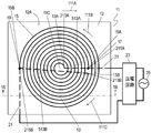
- FIG. 1A is a schematic configuration diagram of a power transmission coil according to an embodiment of the present invention.
- 1B is a cross-sectional view of the power transmission coil shown in FIG. 1A taken along line 1B-1B.
- FIG. 2 is a schematic configuration diagram of another power transmission coil in the embodiment.
- FIG. 3 is a schematic configuration diagram of still another power transmission coil according to the embodiment.
- FIG. 4A is a schematic configuration diagram of a non-contact power feeding device using a power transmission coil in the embodiment.
- 4B is a cross-sectional view of the non-contact power feeding device shown in FIG. 4A along line 4B-4B.
- FIG. 5 is an exploded view of a conventional antenna device.
- FIG. 1A is a schematic configuration diagram of a power transmission coil 11 according to an embodiment of the present invention.
- 1B is a cross-sectional view of power transmission coil 11 shown in FIG. 1A along line 1B-1B.
- the power transmission coil 11 includes a plurality of planar coils 13 and 15 arranged concentrically in the same plane.
- the planar coils 13 and 15 are electrically connected in parallel.
- the planar coils 13 and 15 are configured such that current flows in the same direction.
- planar coils 13 and 15 are concentrically arranged around the center point 11C in the same plane, it is not necessary to stack a plurality of coils, and the power transmission coil 11 can be thinned. Moreover, since the planar coils 13 and 15 are connected in parallel, the impedance is lowered. Further, since current flows in the same direction in the planar coils 13 and 15, the cancellation of the magnetic field in the vertical direction between the planar coils 13 and 15 is reduced. From these things, the power transmission efficiency of the power transmission coil 11 can be improved.
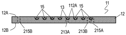
- the power transmission coil 11 includes a base 12 and planar coils 13 and 15 disposed on the surface 12A of the base 12.
- the substrate 12 has a plate shape having a surface 12A and a surface 12B opposite to the surface 12A.
- the planar coils 13 and 15 have a spiral shape extending around the center point 11C.
- the planar coil 13 is disposed inside the planar coil 15, and the planar coil 15 is disposed so as to surround the planar coil 13 outside the planar coil 13.
- a groove 112 ⁇ / b> A is formed on the surface 12 ⁇ / b> A of the base 12.
- the planar coils 13 and 15 are composed of litz wires inserted into the groove 112A.
- the base material 12 is made of a resin that is easy to process.
- the present invention is not limited to this.
- an insulating material having a high magnetic permeability such as a grooved ferrite substrate may be used. In this case, the groove processing is more difficult than the resin, but the leakage magnetic flux can be reduced and the power transmission efficiency can be increased.
- the planar coils 13 and 15 are composed of litz wires inserted into the grooves 112A formed on the surface 12A of the base material 12, but may be embedded in the base material 12, You may form with the conductor foil provided in the surface 12A.
- the planar coil 13 is wound a predetermined number of times in a counterclockwise direction around the center point 11C from the end 13A located in the vicinity of the center of the substrate 12, and extends to the end 13B.
- the end 13B is located farther from the center point 11C than the end 13A.
- the end 13A is located inside the spiral shape of the planar coil 13, and the end 13B is located outside the spiral shape.
- the planar coil 13 is drawn from the substrate 12 at the end 13B.
- the base material 12 is formed with through holes 213A and 213B which are located at the ends 13A and 13B of the planar coil 13 and penetrate from the surface 12A to the surface 12B.
- the litz wire constituting the planar coil 13 is led out from the ends 13A and 13B to the surface 12B of the substrate 12 through the through holes 213A and 213B.
- the ends 13A and 13B are located in the direction 111A from the center point 11C.
- the planar coil 15 extends from the end 15A located near the end 13B of the planar coil 13 to the end 15B by being wound a predetermined number of times counterclockwise in a spiral manner around the center point 11C.
- the end 15B is located farther from the center point 11C than the end 15A.
- the end 15A is located inside the spiral shape of the planar coil 15, and the end 15B is located outside the spiral shape.
- the planar coil 15 is drawn from the substrate 12 at the end 15B.
- the base material 12 is formed with through holes 215A and 215B that are located at the ends 15A and 15B of the planar coil 15 and penetrate from the surface 12A to the surface 12B.
- the litz wire constituting the planar coil 15 is led out from the ends 15A and 15B to the surface 12B of the substrate 12 through the through holes 215A and 215B.
- both the planar coils 13 and 15 are wound counterclockwise (circumferential direction 111B) around the center point 11C as viewed from the surface 12A. It may be wound around (around direction 111C opposite to the turn direction 111B).
- connection point 17 is located at the end 15A, and the end 13A is connected to the end 15A at the connection point 17 via a conducting wire 513A.
- connection point 19 is located at the end 15B, and the end 13B is connected to the end 15B at the connection point 19 via a conducting wire 513B.
- the thickness of the power transmission coil 11 is the thickness of one substrate 12, and the thickness is reduced. Can do.
- planar coils 13 and 15 have a circular spiral shape, this is not limited to a circular shape and may be a spiral shape such as an ellipse or a polygon.
- planar coils 13 and 15 are made to have substantially the same impedance. That is, by adjusting the thickness and length of the litz wire constituting the planar coils 13 and 15, the impedance of both is substantially within an error range (including measurement error and litz wire thickness and length error). It is adjusted to be equal. Since the planar coils 13 and 15 are connected in parallel, if the impedances of the planar coils 13 and 15 are different from each other, the current concentrates on the planar coil having a low impedance. As a result, the possibility that the life of the planar coil is shortened increases. Therefore, it is desirable to configure the planar coils 13 and 15 so that both impedances are substantially equal.
- the lead-out cable 21 is connected to the connection points 17 and 19.
- the lead cable 21 is electrically connected to the power transmission circuit 23.
- the power transmission circuit 23 has a function of converting the power of the system power supply 25 into a waveform suitable for power transmission.
- the electrical characteristics such as the voltage and frequency of the waveform may be appropriately determined according to the required power transmission specifications.
- the ends 13A and 15A located inside the spiral shapes of the planar coils 13 and 15 are electrically connected to each other, and the ends 13B and 15B located outside are electrically connected to each other. 15 are connected in parallel. Since the planar coils 13 and 15 are wound from the ends 13A and 15A to the ends 13B and 15B in the same circumferential direction 111B around the center point 11C, the current flowing from the power transmission circuit 23 is generated between the planar coils 13 and 15. It flows in the same direction (circumferential direction 111B or circular direction 111C) around the center point 11C. Thereby, since cancellation of the magnetic field in both the up-down directions is reduced, the efficiency of power transmission is improved.
- the efficiency when power transmission was performed using the power transmission coil 11 was measured.
- the efficiency of the power transmission coil of the comparative example provided with the base material 12 and the one planar coil which consists of one litz wire arranged on the surface 12A of the base material 12 as a comparison object was also measured.
- the power transmission coil 11 and the power transmission coil of the comparative example were used on the power transmission side, and a planar coil having the same shape and number of turns as the planar coil 13 was used as the power transmission coil on the power receiving side.
- the efficiency of the power transmission coil of the comparative example is 90%, and the efficiency of the power transmission coil 11 in the embodiment is 90.5%, which is 0.5 points higher than the power transmission coil of the comparative example. ing.
- the reason why the efficiency is improved in this way is that the planar coils 13 and 15 are connected in parallel, the impedance is reduced, and the direction of the current flowing through the planar coils 13 and 15 is the same, and the vertical direction of the two is the same. In other words, the canceling of the magnetic field at has been reduced. Since the power transmission coil 11 according to the embodiment can reduce the impedance, a large current can be passed through the power transmission coil 11 and a larger amount of power can be transmitted.
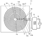
- FIG. 2 is a schematic configuration diagram of another power transmission coil 111 in the embodiment.
- the same reference numerals are assigned to the same parts as those of the power transmission coil 11 shown in FIG. 1A.
- the lead-out cable 21 extending from the parallel connection points 17 and 19 of the planar coils 13 and 15 is drawn out along the same line 111L in substantially the same direction.
- the lead-out direction of the lead-out cable 21 electrically connected to the inner end 13A of the planar coil 13 and the inner end 15A of the planar coil 15 is the same as that of the power transmission coil 11 shown in FIG. 12 on the right side. That is, the ends 13A and 15A are located in the direction 111A from the center point 11C.
- the lead-out direction of the lead-out cable 21 electrically connected to the end 13B of the planar coil 13 and the end 15B of the planar coil 15 is lower left of the base material 12 in the power transmission coil 11 shown in FIG.
- the ends 13B and 15B are also located in the direction 111A from the center point 11C. Accordingly, in the power transmission coil 111, the lead cables 21 from the parallel connection points 17 and 19 at the ends of the planar coils 13 and 15 are drawn along the same line 111L in substantially the same direction.
- drawing along substantially the same direction along the same line 111L means that the lead-out cables 21 are drawn out along the same line 111L in the same direction as close as possible without being in electrical contact with each other. Is defined to mean. Therefore, in the power transmission coil 111, as shown in FIG. 2, the lead cables 21 are arranged in the right direction of the base material 12 in a state of approaching without contacting each other.
- each lead-out cable 21 is drawn out in substantially the same direction, so that the wiring between each lead-out cable 21 and the power transmission circuit 23 can be easily routed.
- each lead-out cable 21 is arranged in parallel in the right direction of the base material 12.
- the drawer cable 21 may be twisted together. In this case, since the magnetic field generated from each lead-out cable 21 is further canceled out, it is possible to further increase the efficiency.
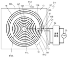
- FIG. 3 is a schematic configuration diagram of still another power transmission coil 211 in the embodiment. 3, the same reference numerals are assigned to the same portions as those of the power transmission coil 11 shown in FIG. 1A.
- the winding directions of the planar coils 13 and 15 are opposite to each other.
- the planar coils 13 and 15 can be configured in a single stroke with a single litz wire, so that the power transmission coil 211 can be made thin and highly efficient, and can be easily manufactured.
- the configuration of the planar coil 13 is the same as that of the power transmission coils 11 and 111 shown in FIGS. 1A and 2, and the planar coil 13 has an end 13A in the circumferential direction 111B around the center point 11C.
- the end 15 ⁇ / b> B of the planar coil 15 exists near the outer edge 12 ⁇ / b> C of the substrate 12, and is wound inward from there. That is, the planar coil 15 extends from the end 15A to the end 15B in the circumferential direction 111C opposite to the circumferential direction 111B around the center point 11C.
- the end 15A of the planar coil 15 is electrically connected to the end 13B of the planar coil 13 at the connection point 17 located at the end 15A.
- the planar coils 13 and 15 can be formed by a single litz wire folded at the connection point 17. Note that the end 13A of the planar coil 13 and the end 15B of the planar coil 15 are electrically connected at a connection point 19 located at the end 15B. As a result, the planar coils 13 and 15 are electrically connected in parallel.
- a lead-out cable 21 is electrically connected to the connection points 17 and 19, respectively.
- the connection point 17 is a point where the lead-out cable 21 is connected to the folded portion of one litz wire.
- planar coils 13 and 15 extend from the inner circumferential ends 13A and 15B in opposite circumferential directions 111B and 111C around the center point 11C, the planar coils 13 and 15 are counterclockwise due to the above-described current. It flows from the ends 13A and 15A to the ends 13B and 15B in the rotation direction 111B around the center point 11C.
- the power transmission coil 211 can be formed in which mutual cancellation of the magnetic field in the vertical direction is reduced. As a result, as with the power transmission coils 11 and 111, a highly efficient power transmission coil 211 can be realized.
- the winding direction of the planar coils 13 and 15 is not limited to that shown in FIG. 3, and any of them may be wound in the direction opposite to that in FIG.
- the planar coils 13 and 15 need to be wound from the inner ends 13A and 15A in mutually opposite circulation directions.
- the planar coils 13 and 15 are formed by folding one litz wire, the impedances of the planar coils 13 and 15 are substantially equal by adjusting their lengths. What should I do.
- each lead-out cable 21 is substantially in the same direction (the right side of the base material 12 in FIG. 3), that is, the center point. 11C is arranged so as to be drawn in the direction 111A.
- the configuration is not limited to this configuration, and the drawing direction of each drawing cable 21 may be different from that of the power transmission coil 11 shown in FIG. 1A.
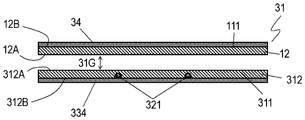
- FIG. 4A is a schematic configuration diagram of the non-contact power feeding device 31 using the power transmission coil 111 in the embodiment.
- the non-contact power feeding device 31 includes the power transmission coil 111 shown in FIG. 2 and another power transmission coil 311.
- the power transmission coil 311 has the same structure as the power transmission coil 111 shown in FIG. 2, that is, the base material 312 and the planar coil 313 shown in FIG. 315 and a drawer cable 321.
- the planar coils 313 and 315 are connected in parallel and are drawn out of the base material 312 by a lead-out cable 321.
- the base materials 12 and 312 are arranged to face each other.
- the lead-out cable 21 of the power transmission coil 11 having the base material 12 located on the back side is electrically connected to the system power supply 25 via the power transmission circuit 23.
- This configuration is the same as in the second embodiment. Since the power transmission coil 111 on the back side is connected to the power transmission circuit 23, it functions as a power transmission coil on the power transmission side.
- the power transmission coil 311 having the base material 312 located on the near side includes the planar coils 313 and 315 having the same shape as the planar coils 13 and 15, respectively. Accordingly, the power transmission coil 311 on the near side has the same shape as the power transmission coil 111 on the back side.
- the lead-out cable 321 of the power transmission coil 311 on the near side is arranged below the power transmission coil 311 as shown in FIG. 4A.
- the direction of the lead-out cables 21 and 321 of the power transmission coils 111 and 311 is not limited to that of FIG. 4A, and may be configured to be drawn out from any direction.
- the lead-out cable 321 in the power transmission coil 311 on the front side is electrically connected to the load 29 via the power receiving circuit 27. Accordingly, the power transmission coil 311 on the near side functions as the power transmission coil 311 on the power receiving side.
- FIG. 4B is a cross-sectional view of the non-contact power feeding device 31 shown in FIG. 4A taken along line 4B-4B.
- the power transmission coils 111 and 311 face each other so that the surfaces 12A and 312A of the base materials 12 and 312 face each other.
- the power transmission coils 111 and 311 are ferrites provided on the surfaces 12B and 312B of the base materials 12 and 312, respectively. It further has thin magnetic materials 34 and 334 such as sheets. Accordingly, the litz wire for drawing arranged on the surfaces 12B and 312B of the substrate 12 is not shown in FIG. 4A.
- the power of the system power supply 25 is converted into a waveform for performing non-contact power feeding by the power transmission circuit 23 and supplied to the power transmission coil 111 on the power transmission side.
- Power is transmitted from the power transmission coil 111 on the power transmission side to the power transmission coil 311 on the power reception side in a state where the surface 312A of the base material 12 faces the surface 312A of the base material 312 with a predetermined gap 31G.
- This power is converted into a power waveform suitable for the load 29 by the power receiving circuit 27 and then supplied to the load 29. Thereby, the electric power of the system power supply 25 can be supplied to the load 29 in a non-contact manner.
- the predetermined gap 31G is determined in advance as a gap required when performing non-contact power feeding.
- the load 29 may be configured to consume power, or may be configured to store power such as a secondary battery. Here, these are collectively referred to as a load 29.
- the planar coils 13 and 15 in the power transmission coil 111 on the power transmission side have the same shape as the planar coils 313 and 315 in the power transmission coil 311 on the power reception side, respectively.
- the power transmission coil 111 on the power transmission side and the power transmission coil 311 on the power reception side face each other. Accordingly, the magnetic field generated by the power transmission coil 111 on the power transmission side is magnetically coupled to the power transmission coil 311 on the power reception side facing each other with a predetermined gap 31G. At this time, the magnetic flux generated by the generated magnetic field is coupled to the power transmission coil 311 on the power receiving side at the shortest distance with a predetermined gap 31G. Therefore, it is possible to configure the power transmission coils 111 and 311 with higher efficiency compared to the case of using a normal planar coil.
- the power in the power transmission coils 111 and 311 of the non-contact power feeding device 31 in the embodiment is compared with the power transmission efficiency in the power transmission coil of the comparative example in which the planar coil is formed by only one litz wire.
- the transmission efficiency is improved by about 1.2%.
- the power transmission coils 111 and 311 can be more efficient than the power transmission coil 11 illustrated in FIG. 1A.
- the receiving-side planar coils 313 and 315 and the transmitting-side planar coils 13 and 15 have the same shape, and the transmitting-side power transmission coil 111 and the receiving-side power transmission coil 311 face each other. Therefore, it is possible to realize the power transmission coil 111 capable of further increasing efficiency in addition to thinning.
- the power transmission coil having the same shape as the power transmission coil 111 shown in FIG. 2 is used on both the power receiving side and the power transmission side, but the power transmission coils 11 and 211 shown in FIG. 1A and FIG. You may use for the power receiving side and the power transmission side.
- the power transmission coils on the power reception side and the power transmission side are not the same shape, a positional shift occurs and the efficiency decreases.
- the power transmission coil 11 shown in FIG. 1A is used on both the power reception side and the power transmission side, or the power transmission coil 211 shown in FIG. 3 is used on both the power reception side and the power transmission side.
- a device is obtained.
- the litz wire is used for the planar coils 13 and 15.
- the present invention is not limited to this, and one copper is used when used in a frequency range where the influence of the skin effect is small. A configuration using lines may also be used.
- the power transmission coils 11, 111, and 211 are configured to use two planar coils 13 and 15 as planar coils.
- the present invention is not limited to this, and the power transmission coil in the embodiment is a base material.
- the power transmission coils 11, 111, and 211 may be used not only for non-contact power feeding but also as a thin transformer coil.
- the power transmission coil according to the present invention can be reduced in thickness and efficiency, it is particularly useful as a power transmission coil for non-contact power feeding or a transformer.
- Non-contact power feeding device 111 Power transmission coil (power transmission coil on the power transmission side) 211 Power transmission coil 311 Power transmission coil (another power transmission coil, power transmission coil on the power receiving side) 313 planar coil (second planar coil, another planar coil) 315 planar coil (second planar coil, another planar coil)
Landscapes
- Engineering & Computer Science (AREA)
- Power Engineering (AREA)
- Computer Networks & Wireless Communication (AREA)
- Physics & Mathematics (AREA)
- Electromagnetism (AREA)
- Coils Of Transformers For General Uses (AREA)
Abstract
La présente invention a trait à une bobine de transmission électrique fournie avec une pluralité de bobines planes disposées de façon concentrique les unes par rapport aux autres, sur le même plan. Les bobines planes sont connectées en parallèle les unes par rapport aux autres. La pluralité de bobines planes est connectée de telle sorte que le courant circule à travers les bobines planes dans la même direction. Cette bobine de transmission de courant est fine, et son efficacité de transmission de courant est élevée.
Applications Claiming Priority (2)
| Application Number | Priority Date | Filing Date | Title |
|---|---|---|---|
| JP2011170686 | 2011-08-04 | ||
| JP2011-170686 | 2011-08-04 |
Publications (1)
| Publication Number | Publication Date |
|---|---|
| WO2013018268A1 true WO2013018268A1 (fr) | 2013-02-07 |
Family
ID=47628823
Family Applications (1)
| Application Number | Title | Priority Date | Filing Date |
|---|---|---|---|
| PCT/JP2012/003979 Ceased WO2013018268A1 (fr) | 2011-08-04 | 2012-06-19 | Bobine de transmission électrique et appareil d'alimentation en courant sans contact utilisant celle-ci |
Country Status (1)
| Country | Link |
|---|---|
| WO (1) | WO2013018268A1 (fr) |
Cited By (5)
| Publication number | Priority date | Publication date | Assignee | Title |
|---|---|---|---|---|
| WO2014181227A1 (fr) * | 2013-05-09 | 2014-11-13 | Tyco Electronics (Shanghai) Co. Ltd. | Circuit d'alimentation en energie sans contact |
| WO2015027917A1 (fr) * | 2013-08-29 | 2015-03-05 | 海尔集团技术研发中心 | Procédé d'alimentation électrique sans fil, appareil d'alimentation électrique sans fil et système d'alimentation électrique sans fil |
| JP2016513366A (ja) * | 2013-02-11 | 2016-05-12 | ザ リージェンツ オブ ザ ユニバーシティ オブ カリフォルニア | 分数巻数コイル巻線 |
| US20170155280A1 (en) * | 2015-11-27 | 2017-06-01 | Canon Kabushiki Kaisha | Power transmission apparatus wirelessly transmitting power to power receiving apparatus |
| US10511191B2 (en) | 2015-07-09 | 2019-12-17 | Qualcomm Incorporated | Apparatus and methods for wireless power transmitter coil configuration |
Citations (2)
| Publication number | Priority date | Publication date | Assignee | Title |
|---|---|---|---|---|
| JP2008136311A (ja) * | 2006-11-29 | 2008-06-12 | Asuka Electron Kk | 複合平面コイル |
| WO2011036863A1 (fr) * | 2009-09-24 | 2011-03-31 | パナソニック電工株式会社 | Système chargeur sans contact |
-
2012
- 2012-06-19 WO PCT/JP2012/003979 patent/WO2013018268A1/fr not_active Ceased
Patent Citations (2)
| Publication number | Priority date | Publication date | Assignee | Title |
|---|---|---|---|---|
| JP2008136311A (ja) * | 2006-11-29 | 2008-06-12 | Asuka Electron Kk | 複合平面コイル |
| WO2011036863A1 (fr) * | 2009-09-24 | 2011-03-31 | パナソニック電工株式会社 | Système chargeur sans contact |
Cited By (8)
| Publication number | Priority date | Publication date | Assignee | Title |
|---|---|---|---|---|
| JP2016513366A (ja) * | 2013-02-11 | 2016-05-12 | ザ リージェンツ オブ ザ ユニバーシティ オブ カリフォルニア | 分数巻数コイル巻線 |
| US10394270B2 (en) | 2013-02-11 | 2019-08-27 | The Regents Of The University Of California | Fractional turn coil winding |
| US11137789B2 (en) | 2013-02-11 | 2021-10-05 | The Regents Of The University Of California | Fractional turn coil winding |
| WO2014181227A1 (fr) * | 2013-05-09 | 2014-11-13 | Tyco Electronics (Shanghai) Co. Ltd. | Circuit d'alimentation en energie sans contact |
| US9941744B2 (en) | 2013-05-09 | 2018-04-10 | Tyco Electronics (Shanghai) Co. Ltd. | Non-contact power supply circuit |
| WO2015027917A1 (fr) * | 2013-08-29 | 2015-03-05 | 海尔集团技术研发中心 | Procédé d'alimentation électrique sans fil, appareil d'alimentation électrique sans fil et système d'alimentation électrique sans fil |
| US10511191B2 (en) | 2015-07-09 | 2019-12-17 | Qualcomm Incorporated | Apparatus and methods for wireless power transmitter coil configuration |
| US20170155280A1 (en) * | 2015-11-27 | 2017-06-01 | Canon Kabushiki Kaisha | Power transmission apparatus wirelessly transmitting power to power receiving apparatus |
Similar Documents
| Publication | Publication Date | Title |
|---|---|---|
| US11837877B2 (en) | Coil module, wireless charging transmitting apparatus, receiving apparatus, system, and terminal | |
| US11978583B2 (en) | Coil module, wireless charging transmitting apparatus, wireless charging receiving apparatus, wireless charging system, and mobile terminal | |
| US10122183B2 (en) | Thin film coil and electronic device having the same | |
| CN107275063B (zh) | 供电线圈单元、无线供电装置以及无线电力传输装置 | |
| US10158256B2 (en) | Contactless connector system tolerant of position displacement between transmitter coil and receiver coil and having high transmission efficiency | |
| JP6743432B2 (ja) | コイル装置 | |
| US10381148B2 (en) | Transformer and power converter using the same | |
| US11515084B2 (en) | Magnetic component and wireless power-transferring device including the same | |
| JP3226466U (ja) | コイルモジュールおよびそれを用いたワイヤレス電気エネルギー送信回路 | |
| JP6607007B2 (ja) | コイル装置 | |
| WO2020029664A1 (fr) | Module de bobine, appareil de transmission de charge sans fil, appareil de réception, système et terminal | |
| US10270290B2 (en) | Power supply device | |
| US10002708B2 (en) | Coil unit and wireless power transmission device | |
| CN110289156A (zh) | 线圈绕组、线圈模组、发射装置、接收装置、系统和终端 | |
| WO2013018268A1 (fr) | Bobine de transmission électrique et appareil d'alimentation en courant sans contact utilisant celle-ci | |
| JP2017212880A (ja) | ワイヤレス電力伝送装置 | |
| JP2016076645A (ja) | 平面コイル | |
| US9633762B2 (en) | Cable | |
| EP2998971B1 (fr) | Convertisseur de puissance comprenant un dispositif d'inductance avec blindage | |
| US9991749B2 (en) | Coil unit, wireless power feeding device, wireless power receiving device, and wireless power transmission device | |
| CN213660188U (zh) | 降低磁场干扰的变压器装置 | |
| US10862544B2 (en) | Magnetic coupler and communication system | |
| WO2021131607A1 (fr) | Dispositif de détection d'objet étranger, dispositif de transmission d'énergie, dispositif de réception d'énergie et système de transmission d'énergie | |
| US9935500B2 (en) | Coil unit, wireless power feeding device, wireless power receiving device, and wireless power transmission device | |
| WO2015122344A1 (fr) | Unité de bobines et système d'alimentation électrique la comportant |
Legal Events
| Date | Code | Title | Description |
|---|---|---|---|
| 121 | Ep: the epo has been informed by wipo that ep was designated in this application |
Ref document number: 12819881 Country of ref document: EP Kind code of ref document: A1 |
|
| NENP | Non-entry into the national phase |
Ref country code: DE |
|
| 122 | Ep: pct application non-entry in european phase |
Ref document number: 12819881 Country of ref document: EP Kind code of ref document: A1 |
|
| NENP | Non-entry into the national phase |
Ref country code: JP |