WO2013018603A1 - Procédé de fabrication de dispositif d'onde acoustique - Google Patents
Procédé de fabrication de dispositif d'onde acoustique Download PDFInfo
- Publication number
- WO2013018603A1 WO2013018603A1 PCT/JP2012/068786 JP2012068786W WO2013018603A1 WO 2013018603 A1 WO2013018603 A1 WO 2013018603A1 JP 2012068786 W JP2012068786 W JP 2012068786W WO 2013018603 A1 WO2013018603 A1 WO 2013018603A1
- Authority
- WO
- WIPO (PCT)
- Prior art keywords
- metal
- layer
- bonding
- metal layer
- piezoelectric
- Prior art date
- Legal status (The legal status is an assumption and is not a legal conclusion. Google has not performed a legal analysis and makes no representation as to the accuracy of the status listed.)
- Ceased
Links
Images




Classifications
-
- H—ELECTRICITY
- H03—ELECTRONIC CIRCUITRY
- H03H—IMPEDANCE NETWORKS, e.g. RESONANT CIRCUITS; RESONATORS
- H03H3/00—Apparatus or processes specially adapted for the manufacture of impedance networks, resonating circuits, resonators
- H03H3/007—Apparatus or processes specially adapted for the manufacture of impedance networks, resonating circuits, resonators for the manufacture of electromechanical resonators or networks
- H03H3/02—Apparatus or processes specially adapted for the manufacture of impedance networks, resonating circuits, resonators for the manufacture of electromechanical resonators or networks for the manufacture of piezoelectric or electrostrictive resonators or networks
-
- H—ELECTRICITY
- H03—ELECTRONIC CIRCUITRY
- H03H—IMPEDANCE NETWORKS, e.g. RESONANT CIRCUITS; RESONATORS
- H03H3/00—Apparatus or processes specially adapted for the manufacture of impedance networks, resonating circuits, resonators
- H03H3/007—Apparatus or processes specially adapted for the manufacture of impedance networks, resonating circuits, resonators for the manufacture of electromechanical resonators or networks
- H03H3/08—Apparatus or processes specially adapted for the manufacture of impedance networks, resonating circuits, resonators for the manufacture of electromechanical resonators or networks for the manufacture of resonators or networks using surface acoustic waves
Definitions
- the present invention relates to a method of manufacturing an acoustic wave device having a structure in which a piezoelectric thin film is bonded to a support substrate.
- a piezoelectric thin film is bonded to a support substrate.
- various methods have been proposed and adopted as a bonding method between a piezoelectric thin film and a support substrate.
- hydrophilization bonding in a bonding method called hydrophilization bonding (see Patent Document 1), first, an inorganic oxide layer is formed on each of a thin-film-side bonded surface and a supporting substrate-side bonded surface that are mirror-finished. Next, a hydroxyl group is formed on the surface of the inorganic oxide layer. Next, the surface of the inorganic oxide layer on the thin film side and the surface of the inorganic oxide layer on the support substrate side are overlapped, whereby the inorganic oxide layer on the thin film side and the inorganic on the support substrate side are formed by hydrogen bonding between hydroxyl groups. Bonding with the oxide layer. Next, by heat treatment at 200 ° C. or higher, H 2 O is desorbed from the hydrogen-bonded hydroxyl groups, thereby increasing the bonding strength between the inorganic oxide layer on the thin film side and the inorganic oxide layer on the support substrate side. Greatly improve.
- the mirror-finished joining surface on the thin film side and the joining surface on the support substrate side are sputter-etched in an inert gas atmosphere or in a vacuum to start from the surface. The contamination is removed and the surface is activated. In this state, the bonding surface on the thin film side and the bonding surface on the support substrate side are overlapped to firmly bond the bonding surface on the thin film side and the bonding surface on the support substrate side in a non-heating environment.
- metal diffusion joining In a joining method called metal diffusion joining, first, a metal layer is formed on each of the joining surface on the thin film side and the joining surface on the support substrate side. Next, by overlapping the metal layer on the thin film side and the metal layer on the support substrate side, the metal layer on the thin film side and the metal layer on the support substrate side are strong in an unheated environment by crystal rearrangement between the metal layers. To be joined.
- activated bonding and metal diffusion bonding can achieve strong bonding in a non-heated environment, and the difference in linear expansion coefficient between the piezoelectric body and the support substrate is a limitation on bonding. No.
- activated bonding has a low tolerance for surface contamination, and it is necessary to strictly manage the bonding environment during bonding. For this reason, it is difficult to stably realize strong bonding when continuously performing active bonding on a large number of objects to be processed.
- metal diffusion bonding can stably realize strong bonding, but since an acoustic wave device has a metal bonding layer, the types of devices that can be used are limited. For example, in a high-frequency device such as a filter or a duplexer, characteristic deterioration may be caused by leakage of a high-frequency signal to a metal bonding layer, and it is difficult to use metal diffusion bonding.
- an object of the present invention is to realize a method for manufacturing an acoustic wave device in which the type of device is not limited while stably realizing strong bonding.
- the method for manufacturing an acoustic wave device includes a first metal layer forming step, a second metal layer forming step, a metal bonding layer forming step, and a metal oxide layer forming step.
- the first metal layer forming step is a step of forming the first metal layer on the bonding surface side of the piezoelectric substrate made of a piezoelectric body.
- the second metal layer forming step is a step of forming the second metal layer on the bonding surface side of the support substrate. In the metal bonding layer forming step, the first metal layer and the second metal layer are overlapped, and the crystal of the first metal layer and the crystal of the second metal layer are rearranged to form the metal bonding layer. It is a process.
- the metal oxide layer forming step is a step of forming a metal oxide layer by oxidizing the metal bonding layer.
- the piezoelectric substrate and the support substrate are metal diffusion bonded via the metal bonding layer, it is possible to stably realize strong bonding.
- the conductivity of the metal bonding layer which causes deterioration of characteristics in the acoustic wave device, can be sufficiently lowered, greatly restricting the device type. To be relaxed.
- the above-described method for manufacturing an acoustic wave device preferably includes a first oxide layer forming step of forming a first oxide layer on the bonding surface side of the piezoelectric substrate.
- a second oxide layer forming step of forming a second oxide layer on the bonding surface side of the support substrate.
- the metal layer is made of a material having a negative oxide generation free energy.
- the metal oxide layer preferably has a thickness of 50 nm or less.
- the first oxide layer and the second oxide layer serve as an oxygen supply source, the time required for oxidation and the heating temperature in the case of oxidation by heating can be significantly reduced.
- the first metal layer and the second metal layer are made of the same material.
- the first metal layer forming step and the second metal layer forming step can be made substantially the same manufacturing step, and the formation of the first and second metal layers is facilitated.
- the bonding surface between the first metal layer and the second metal layer can be made high quality.
- the first metal layer forming step, the second metal layer forming step, and the metal bonding layer forming step are performed continuously in an inert gas atmosphere or in a vacuum. It is.
- the surfaces of the first and second metal layers are not oxidized by outside air or contaminated with contamination, and the metal bonding layer can be formed by superposing clean surfaces. Therefore, it is possible to realize strong bonding more stably.
- the ion implantation step is a step of implanting ions from the bonding surface side of the piezoelectric substrate.
- the separation step is a step of separating the bonding surface side region as a piezoelectric thin film from the defect layer of the piezoelectric substrate due to the ions by heating.
- the piezoelectric thin film can be formed with a stable film thickness and a desired crystal orientation, and the material utilization efficiency of the piezoelectric substrate can be increased.
- the ion distribution density is biased in the thickness direction of the piezoelectric thin film.
- the piezoelectric thin film is slightly warped, and difficulty in joining to the support substrate is likely to occur.
- the utility is very large.
- the piezoelectric substrate is preferably a piezoelectric single crystal substrate. In these manufacturing methods, it is possible to obtain an acoustic wave device that prevents signal leakage from the functional electrode while stably realizing strong bonding by utilizing crystal rearrangement between metal layers.
- the piezoelectric substrate and the support substrate can be joined firmly and stably. Since the metal bonding layer is oxidized to form a metal oxide layer, an elastic wave device without the metal bonding layer can be obtained, and the presence of the metal bonding layer does not cause deterioration of the characteristics of the elastic wave device. Restrictions on types are relaxed.
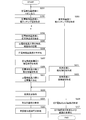
- FIG. 1 is a diagram for explaining a manufacturing flow of the SAW device of this embodiment.
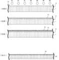
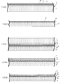
- 2 to 4 are schematic diagrams in each process of the manufacturing flow.
- the piezoelectric single crystal substrate 1 is prepared, and ions are implanted from the main surface 1A (joint surface 1A) side of the piezoelectric single crystal substrate 1 (S101).
- the defect layer 2 is formed at a predetermined depth from the bonding surface 1A of the piezoelectric single crystal substrate 1.
- This step corresponds to the ion implantation step in this embodiment.
- the defect layer 2 is a region where defects due to atoms of ions implanted into the piezoelectric single crystal substrate 1 are concentrated. This process is performed as a pre-process for separating the piezoelectric single crystal thin film 11 (not shown) having a very thin film thickness from the piezoelectric single crystal substrate 1 later.
- the piezoelectric single crystal substrate 1 used here is an LT substrate.
- the ions are hydrogen ions.
- hydrogen ions are implanted into the piezoelectric single crystal substrate 1 at an acceleration voltage of 80 KeV and a dose of 1.0 ⁇ 10 17 atoms / cm 2 .
- the defect layer 2 is formed at a depth of about 550 nm from the bonding surface 1A.
- the formation position of the defect layer 2 is determined by the acceleration voltage at the time of ion implantation. For example, when the defect layer 2 is formed at about half the depth, the acceleration voltage may be about halved.
- the material of the piezoelectric single crystal substrate 1 is not limited to the LT substrate, but may be LN (LiNbO 3 ), LBO (Li 2 B 4 O 7 ), langasite (La 3 Ga 5 SiO 14 ), KN (KNbO 3 ), etc.
- a piezoelectric material may be selected as appropriate.
- ions to be implanted may be appropriately selected from helium ions, argon ions, etc. in addition to hydrogen ions.
- a dielectric layer 21 is formed on the bonding surface 1A of the piezoelectric single crystal substrate 1 (S102).
- the dielectric layer 21 is provided to confine the surface acoustic wave in the SAW device and obtain good device characteristics.
- the dielectric layer 21 used here is a laminated film of a silicon oxide film (not shown) having a thickness of 700 nm and an aluminum nitride film (not shown) having a thickness of 1400 nm.
- the dielectric layer 21 is not an essential component and may not be provided.
- an oxide layer 31 is formed on the surface of the dielectric layer 21 (S103).
- This step corresponds to the first oxide layer forming step in the present embodiment.
- the surface of the oxide layer 31 is preferably planarized by a CMP (Chemical Mechanical Polishing) method or the like.
- the oxide layer 31 used here is a silicon oxide film.
- the oxide layer 31 may be made of any other material as long as it can be a source of oxygen supply to the metal bonding layer 43 (not shown).
- the film thickness may be appropriately adjusted according to the type and film thickness of the metal bonding layer 43 (not shown) so that sufficient oxygen can be supplied to the metal bonding layer 43 (not shown) later.
- the support substrate 12 is prepared, and the oxide layer 32 is formed on the surface of the support substrate 12 (S111).
- This step corresponds to the second oxide layer forming step in this embodiment.
- the surface of the oxide layer 32 is preferably planarized by a CMP method or the like.
- the oxide layer 32 used here is a silicon oxide film.
- the oxide layer 32 may be made of other materials as long as it is a material that later becomes an oxygen supply source to the metal bonding layer 43 (not shown). .
- the film thickness may be appropriately adjusted according to the type and film thickness of the metal bonding layer 43 (not shown) so that sufficient oxygen can be supplied to the metal bonding layer 43 (not shown) later.
- the first and second oxide layers 31 and 32 have an oxygen-rich composition rather than an energetically stable composition ratio as an oxide.
- the metal bonding layer 43 symbol not shown
- the support substrate 12 is an oxide
- the metal bonding layer 43 may be formed without forming a separate oxide layer on the support substrate 12 depending on the type and film thickness of the metal bonding layer 43 (reference symbol not shown). Oxygen for oxidation (not shown) can be sufficiently supplied.
- the support substrate 12 used here is an alumina substrate or a magnesia substrate.
- An alumina substrate or a magnesia substrate is a material having good thermal conductivity and a linear expansion coefficient close to that of a piezoelectric single crystal material.
- the subsequent metal bonding layer 43 Oxidation (not shown) can be performed at a lower temperature and in a shorter time.
- an ultrathin metal layer 41 is sputter-deposited on the surface of the oxide layer 31 on the piezoelectric single crystal substrate 1 side (S121). This step corresponds to the first metal layer forming step in the present embodiment.
- the metal layer 41 used here is a titanium thin film having a thickness of 1 nm or less.
- a very thin metal layer 42 is formed by sputtering on the surface of the oxide layer 32 on the support substrate 12 side (S122). This step corresponds to the second metal layer forming step in the present embodiment.
- the metal layer 42 is also a titanium thin film having a thickness of 1 nm or less.
- the metal layer 42 (reference not shown) on the support substrate 12 side and the metal layer 41 (reference not shown) on the piezoelectric single crystal substrate 1 side are overlapped to form 2 nm.
- a metal bonding layer 43 having the following thickness is formed (S123). This step corresponds to the metal bonding layer forming step in this embodiment.
- the formation process of the metal layers 41 and 42 and the formation process of the metal bonding layer 43 are continuously performed in a high vacuum of 10 ⁇ 6 Pa or less. For this reason, the titanium crystal on the surface on the piezoelectric single crystal substrate 1 side and the titanium crystal on the surface on the support substrate 12 side are rearranged at normal temperature without accompanying oxidation or moisture adsorption due to oxygen in the atmosphere. It will be. As a result, the metal layers 41 and 42 are firmly bonded by crystal rearrangement to form an integrated crystal, and the metal bonding layer 43 is formed.
- the metal layers 41 and 42 constituting the metal bonding layer 43 are preferably the same kind of metal material. This is because, in the case of dissimilar metal materials, a cavity portion may be formed in the bonded metal portion due to a difference in diffusion rate during heating, or the bonding strength may be deteriorated due to segregation.
- the metal layers 41 and 42 are preferably made of a metal material having a large diffusion coefficient (diffusion rate). This is because a metal material having a large diffusion coefficient can provide a large margin regarding the flatness of the joint surface.
- the metal layers 41 and 42 are preferably a metal material having a negative free energy of formation of oxides and are easily oxidized.
- the 1st metal layer 41 and the 2nd metal layer 42 consist of a single element.
- the 1st metal layer 41 and the 2nd metal layer 42 consist of a single element.
- the bonded body of the support substrate 12 and the piezoelectric single crystal substrate 1 firmly bonded via the metal bonding layer 43 is placed in a heating environment of about 250 ° C. (S124). Then, as shown in FIG. 3 (S124), the piezoelectric single crystal substrate 1 (symbol not shown) is separated by the defect layer 2 (symbol not shown), and the piezoelectric single crystal thin film 11 is formed. This step corresponds to the separation step in this embodiment.
- the piezoelectric single crystal thin film 11 having a very thin film thickness with a good film thickness distribution is easily manufactured. be able to.
- the crystal orientation of the piezoelectric single crystal substrate 1 can be arbitrarily set, by forming the piezoelectric single crystal thin film 11 using ion implantation into the piezoelectric single crystal substrate 1, the piezoelectric single crystal substrate 1 is formed.
- the crystal orientation of the crystal thin film 11 can also be set arbitrarily. Thereby, the piezoelectric single crystal thin film 11 having a crystal orientation desirable as the SAW device can be obtained, and the piezoelectric characteristics of the SAW device can be improved.
- the surface of the piezoelectric single crystal thin film 11 is planarized by a CMP method or the like (S125).
- the metal bonding layer 43 (not shown) is oxidized by heating to form a metal oxide layer 44 (S126).
- This step corresponds to the metal oxide layer forming step in this embodiment. Since the oxide layers 31 and 32 are in contact with the metal bonding layer 43 (not shown), oxygen used for the oxidation reaction is supplied from the oxide layers 31 and 32.
- the heating temperature and heating time for this oxidation may be adjusted according to the metal material and thickness of the metal bonding layer 43. For example, when the metal bonding layer 43 is a titanium thin film having a thickness of 1 nm, if the heating temperature is about 300 ° C. and the heating time is about 1 hour, the metal bonding layer 43 is sufficiently oxidized to form the metal oxide layer 44 and can do.
- the heat treatment for oxidizing the metal oxide layer 44 is performed separately from the heat treatment for separating the piezoelectric single crystal thin film 11, but the heat treatment for separating the piezoelectric single crystal thin film 11 is performed.
- the metal oxide layer 44 may be oxidized by adjusting the heating temperature and the heating time. Further, the heat treatment step for oxidizing the metal oxide layer 44 may be performed before the step of planarizing the surface of the piezoelectric single crystal thin film 11.
- the IDT electrode 50 and the wiring pattern 60A necessary for the operation of the SAW device are formed on the surface of the piezoelectric single crystal thin film 11 (S127).
- This step corresponds to the functional electrode forming step in the present embodiment.
- a laminated film of an aluminum film and a titanium film is used as the IDT electrode 50 and the wiring pattern 60A.
- the aluminum film may be formed using an alloy mainly containing aluminum, such as an Al—Cu alloy.
- the two-layer wiring portion 60B covering the wiring pattern 60A is formed to reduce the resistance of the wiring, and the IDT electrode 50 is covered with the insulating protective film 70 (S128). ). Thereafter, the SAW device is manufactured by singulation.
- the bonding strength between the piezoelectric single crystal substrate 1 and the support substrate 12 develops in a non-heated environment, so that heating to develop the bonding strength is unnecessary, and the piezoelectric single crystal substrate 1 Even if the difference in linear expansion coefficient between the support substrate 12 and the support substrate 12 is large, various problems are unlikely to occur during bonding.
- ions atoms are present in the crystal of the piezoelectric single crystal thin film 11, and the distribution density thereof is that of the piezoelectric single crystal thin film 11. Since it is biased in the thickness direction, the piezoelectric single crystal thin film 11 has a film stress.
- the piezoelectric single crystal thin film 11 (piezoelectric single crystal substrate 1) is easily peeled off from the support substrate 12 due to the addition of the film stress and the thermal stress, thereby realizing stable and strong bonding. Difficult to do. Therefore, the method of the present embodiment, in which strong bonding is manifested from the moment of bonding in a non-heated environment, is not affected by thermal stress at the time of bonding, so it is extremely effective for stably realizing strong bonding. It can be said that it is a simple method.
- the metal bonding layer 43 As a metal oxide layer 44 having a low electrical conductivity after bonding, the characteristics of the SAW device can be improved. Will be obtained.
- Table 1 shows the relationship between the thickness of the metal bonding layer and the characteristic deterioration rate.
- the characteristic deterioration referred to here indicates phase float. If this phase float exceeds 5%, it cannot be used as an acoustic wave device.
- the bonding layer thickness is 2.2 nm and the characteristic deterioration rate exceeds 5%. Therefore, the thickness of the metal bonding layer is desirably 2 nm or less. However, since the metal bonding layer is diffused by heating and oxidation, the metal oxide layer is wider than the metal bonding layer. When the thickness of the metal bonding layer is 2 nm or less, the thickness of the metal oxide layer is in a range up to about 50 nm.
- Second Embodiment a method for manufacturing an acoustic wave device according to the second embodiment of the present invention will be described using a method for manufacturing a SAW device as a specific example.
- the piezoelectric single crystal thin film in order to recover the piezoelectricity and crystallinity of the piezoelectric single crystal thin film that is lowered to a certain extent by ion implantation, the piezoelectric single crystal thin film is subjected to high-temperature heat treatment at about 500 ° C., and the support substrate at that time A manufacturing method for avoiding thermal deformation due to a difference in linear expansion coefficient between the piezoelectric single crystal thin film and the piezoelectric single crystal thin film will be described.
- FIG. 5 is a diagram for explaining the manufacturing flow of the SAW device of this embodiment.
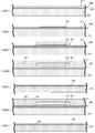
- 6 and 7 are schematic diagrams in each step of the first half of the manufacturing flow.
- the piezoelectric single crystal substrate 201 is prepared, and ions are implanted from the main surface 201A (joint surface 1A) side of the piezoelectric single crystal substrate 201 (S201). As a result, as shown in FIG. 6 (S201), the defect layer 202 is formed at a predetermined depth from the bonding surface 201A of the piezoelectric single crystal substrate 201.
- an etching target layer 291 is formed on the bonding surface 201A of the piezoelectric single crystal substrate 201 (S202).
- the surface of the etching target layer 291 is preferably planarized by a CMP method or the like. This etched layer 291 is to be removed later by etching.
- the layer to be etched 291 used here is a Cu film having a thickness of 3 ⁇ m.
- a temporary support substrate 212 is prepared, and an etching target layer 292 is also formed on the surface of the temporary support substrate 212 (S203).
- the surface of the etching target layer 292 is preferably planarized by a CMP method or the like.
- the temporary support substrate 212 used here is the same material as the piezoelectric single crystal substrate 201.
- the piezoelectric single crystal thin film 211 (symbol not shown) is later subjected to high-temperature heat treatment while being bonded to the temporary support substrate 212 made of the same kind of material. Can be prevented.
- the material of the temporary support substrate 212 may be another material having a small difference in linear expansion coefficient from that of the piezoelectric single crystal thin film 211 (not shown).
- the layer to be etched 292 used here is a Cu film having a thickness of 3 ⁇ m.
- the to-be-etched layer 292 (reference numeral not shown) and the to-be-etched layer 291 (reference numeral not shown) are joined to form the to-be-etched joining layer 293 (S204).
- metal diffusion bonding is used for bonding the etched layer 292 (not shown) and the etched layer 291 (not shown).
- the bonding method here is not limited to metal diffusion bonding, and other bonding methods may be used as long as the bonding method provides a certain degree of bonding strength.
- the bonded body of the temporary support substrate 212 and the piezoelectric single crystal substrate 201 bonded through the bonding layer 293 to be etched is placed in a heating environment of about 250 ° C. (S205). Then, as shown in FIG. 6 (S205), the piezoelectric single crystal substrate 201 (not shown) is separated by the defect layer 202 (not shown) to form a piezoelectric single crystal thin film 211. Subsequently, the bonded body of the temporary support substrate 212 and the piezoelectric single crystal thin film 211 bonded through the bonding layer 293 to be etched is placed in a high temperature environment of about 500 ° C.
- the crystallinity of the piezoelectric single crystal thin film 211 broken by the ion implantation is recovered. Since the temporary support substrate 212 and the piezoelectric single crystal substrate 201 (not shown) have the same material and the same linear expansion coefficient, deformation due to these heat treatments hardly occurs, and the piezoelectric single crystal substrate 201 is not destroyed. It is prevented.
- the surface of the piezoelectric single crystal thin film 211 is planarized by a CMP method or the like (S206).
- the thin film temporary support structure 200 in which the piezoelectric single crystal thin film 211 is bonded to the temporary support substrate 212 through the bonding layer 293 to be etched is configured.
- a dielectric layer 221 is formed on the surface of the piezoelectric single crystal thin film 211 in the thin film temporary support structure 200 (S207).
- an oxide layer 231 is formed on the surface of the dielectric layer 221 in the thin film temporary support structure 200 (S208).
- a support substrate 213 is prepared, and an oxide layer 233 is formed on the surface of the support substrate 213 (S211).
- an extremely thin metal layer 241 is formed on the surface of the oxide layer 231 in the thin film temporary support structure 200 (S221).
- a very thin metal layer 243 is formed on the surface of the oxide layer 233 on the support substrate 213 side (S222).
- the metal layer 243 (reference numeral not shown) on the support substrate 213 side and the metal layer 241 (reference numeral not shown) on the thin film temporary support structure 200 side are overlapped to be metal bonded.
- a layer 244 is formed (S223).
- the formation process of the above-mentioned metal layers 241 and 243 and this bonding process are continuously performed in a high vacuum, and the bonding between the metal layers 241 and 243 is realized by a metal diffusion bonding method.
- the bonded body obtained by bonding the piezoelectric single crystal thin film 211, the temporary support substrate 212, and the support substrate 213 is dipped in an etching solution such as nitric acid, the etched bonding layer 293 is etched, and the etched bonding layer 293 is etched. Then, the temporary support substrate 212 is removed (S224).
- an etching solution such as nitric acid
- the etched bonding layer 293 is etched
- the etched bonding layer 293 is etched.
- the temporary support substrate 212 is removed (S224).
- a metal oxide layer (not shown) is formed by oxidation of the metal bonding layer 244, and an IDT electrode and an insulating protective film are formed.
- the SAW device is manufactured (S225 ⁇ S226 ⁇ S227).
- the second embodiment there is almost no thermal stress that acts on the interface with the piezoelectric substrate, or thermal stress that acts on the interface with the piezoelectric substrate acts on the interface between the support substrate and the piezoelectric substrate. Since the smaller temporary support substrate is formed on the ion-implanted surface side of the piezoelectric substrate, it is possible to suppress the occurrence of defects in the piezoelectric thin film due to heating as compared with the conventional case. In addition, when the acoustic wave device according to the present invention is made of a piezoelectric single crystal material, it can be manufactured while suppressing problems. Since the support substrate itself is formed on the piezoelectric thin film after heating, it is not necessary to consider the thermal stress acting on the interface with the piezoelectric thin film due to heating, and a constituent material having an arbitrary linear expansion coefficient can be selected.
- the selectivity of the combination of the constituent material of the piezoelectric thin film and the constituent material of the support substrate can be enhanced.
- the temperature-frequency characteristics of the filter can be improved by making the linear expansion coefficient of the constituent material of the support substrate much smaller than the linear expansion coefficient of the piezoelectric thin film.
- a piezoelectric single crystal thin film 311 as shown in FIG. 9 (S301) is bonded to the temporary support substrate 312 through the bonding layer 393 to be etched by the same method as in the second embodiment.
- a thin film temporary support structure 300 is formed (S301).
- a lower electrode pattern 321 for driving the BAW device is formed on the surface of the piezoelectric single crystal thin film 311 in the temporary thin film support structure 300 (S302).
- a pattern 331 is formed (S303).
- a membrane support layer 341 is formed on the surface of the piezoelectric single crystal thin film 311 in the thin film temporary support structure 300 so as to cover the sacrificial layer pattern 331 (S304).
- the surface of the membrane support layer 341 is planarized by CMP after sputter deposition.
- the membrane support layer 341 used here is a silicon oxide film and is also used as an oxide layer later.
- a support substrate 313 is prepared, and an oxide layer 343 is formed on the surface of the support substrate 313 (S305).
- an ultrathin metal layer 351 is formed on the surface of the membrane support layer 341 in the thin film temporary support structure 300 (S306).
- an extremely thin metal layer 353 is formed on the surface of the oxide layer 343 on the support substrate 313 side (S307).
- a metal layer 353 (reference numeral not shown) on the support substrate 313 side and a metal layer 351 (reference numeral not shown) on the thin film temporary support structure 300 side are overlapped to form a metal.
- a bonding layer 354 is formed (S308).
- the formation process of the above-mentioned metal layers 351 and 353 and this bonding process are continuously performed in a high vacuum, and the bonding between the metal layers 351 and 353 is realized by a metal diffusion bonding method.
- the bonded body obtained by bonding the piezoelectric single crystal thin film 311, the temporary support substrate 312, and the support substrate 313 is dipped in an etching solution such as nitric acid, the etched bonding layer 393 is etched, and the etched bonding layer 393 is etched. Then, the temporary support substrate 312 is removed (S309).
- a structure in which the piezoelectric single crystal thin film 311 and the support substrate 313 are bonded via the metal bonding layer 354 as shown in FIG. 10 (S309) is formed.
- the metal bonding layer 354 (not shown) is oxidized by heating to form a metal oxide layer 355 (S310).
- the piezoelectric single crystal thin film 311 is opened and an upper electrode pattern for driving the BAW device is formed (S311).
- an etchant is introduced into the sacrificial layer pattern 331 (not shown) from the window of the piezoelectric single crystal thin film 311, and the sacrificial layer pattern 331 (not shown) is removed.
- a membrane space 331A is formed (S312).
- the BAW device is manufactured by dividing into individual pieces.
Landscapes
- Engineering & Computer Science (AREA)
- Manufacturing & Machinery (AREA)
- Physics & Mathematics (AREA)
- Acoustics & Sound (AREA)
- Surface Acoustic Wave Elements And Circuit Networks Thereof (AREA)
Abstract
La présente invention vise à mettre en œuvre un procédé de fabrication d'un dispositif d'onde acoustique par lequel le type de dispositif n'est pas limité, tout en obtenant de façon stable une soudure solide dans un environnement non chauffé. Une couche métallique est formée sur un côté face de soudure d'un substrat monocristallin piézoélectrique (S121). Une couche métallique est formée sur un côté face de soudure d'un substrat support (S122). Les couches métalliques sont superposées, les monocristaux métalliques sont ré-agencés en réseau dans un environnement non chauffé, et une couche de soudure métallique est formée (S123). Par la suite, la couche de soudure métallique est oxydée et une couche d'oxyde métallique est formée (S126).
Priority Applications (1)
| Application Number | Priority Date | Filing Date | Title |
|---|---|---|---|
| JP2013526836A JP5783252B2 (ja) | 2011-07-29 | 2012-07-25 | 弾性波デバイスの製造方法 |
Applications Claiming Priority (2)
| Application Number | Priority Date | Filing Date | Title |
|---|---|---|---|
| JP2011-166581 | 2011-07-29 | ||
| JP2011166581 | 2011-07-29 |
Publications (1)
| Publication Number | Publication Date |
|---|---|
| WO2013018603A1 true WO2013018603A1 (fr) | 2013-02-07 |
Family
ID=47629129
Family Applications (1)
| Application Number | Title | Priority Date | Filing Date |
|---|---|---|---|
| PCT/JP2012/068786 Ceased WO2013018603A1 (fr) | 2011-07-29 | 2012-07-25 | Procédé de fabrication de dispositif d'onde acoustique |
Country Status (2)
| Country | Link |
|---|---|
| JP (2) | JP5783252B2 (fr) |
| WO (1) | WO2013018603A1 (fr) |
Cited By (2)
| Publication number | Priority date | Publication date | Assignee | Title |
|---|---|---|---|---|
| JP2023545695A (ja) * | 2020-10-16 | 2023-10-31 | ソイテック | 膜を移転するための方法 |
| WO2025263426A1 (fr) * | 2024-06-20 | 2025-12-26 | 株式会社村田製作所 | Dispositif à ondes élastiques et son procédé de fabrication |
Families Citing this family (3)
| Publication number | Priority date | Publication date | Assignee | Title |
|---|---|---|---|---|
| WO2020189115A1 (fr) * | 2019-03-15 | 2020-09-24 | 日本電気硝子株式会社 | Substrat composite, dispositif électronique, procédé de fabrication de substrat composite et procédé de fabrication de dispositif électronique |
| MY207300A (en) | 2019-09-05 | 2025-02-15 | Canon Anelva Corp | Chemical bonding method and joined structure |
| WO2022172349A1 (fr) | 2021-02-10 | 2022-08-18 | キヤノンアネルバ株式会社 | Procédé de liaison chimique et composant électronique emballé |
Citations (2)
| Publication number | Priority date | Publication date | Assignee | Title |
|---|---|---|---|---|
| JP2006245990A (ja) * | 2005-03-03 | 2006-09-14 | Matsushita Electric Ind Co Ltd | 弾性表面波素子及びその製造方法 |
| WO2011065317A1 (fr) * | 2009-11-26 | 2011-06-03 | 株式会社村田製作所 | Dispositif piézoélectrique et procédé de fabrication de dispositif piézoélectrique |
Family Cites Families (8)
| Publication number | Priority date | Publication date | Assignee | Title |
|---|---|---|---|---|
| JPH10322158A (ja) * | 1997-05-20 | 1998-12-04 | Asahi Chem Ind Co Ltd | 圧電体基板とその製法及びそれを用いた弾性表面波機能素子 |
| JP2003017967A (ja) * | 2001-06-29 | 2003-01-17 | Toshiba Corp | 弾性表面波素子及びその製造方法 |
| JP3774782B2 (ja) * | 2003-05-14 | 2006-05-17 | 富士通メディアデバイス株式会社 | 弾性表面波素子の製造方法 |
| JP3929983B2 (ja) * | 2004-03-03 | 2007-06-13 | 富士通メディアデバイス株式会社 | 接合基板、弾性表面波素子および弾性表面波デバイス並びにその製造方法 |
| TWI253392B (en) * | 2004-03-29 | 2006-04-21 | Canon Kk | Dielectric member, piezoelectric member, ink jet head, ink jet recording apparatus and producing method for ink jet recording apparatus |
| JP2008109402A (ja) * | 2006-10-25 | 2008-05-08 | Toshiba Corp | 薄膜圧電共振器およびその製造方法 |
| JP5637136B2 (ja) * | 2009-07-07 | 2014-12-10 | 株式会社村田製作所 | 弾性波デバイスおよび弾性波デバイスの製造方法 |
| JP5229399B2 (ja) * | 2009-10-30 | 2013-07-03 | 株式会社村田製作所 | 圧電デバイスの製造方法 |
-
2012
- 2012-07-25 WO PCT/JP2012/068786 patent/WO2013018603A1/fr not_active Ceased
- 2012-07-25 JP JP2013526836A patent/JP5783252B2/ja active Active
-
2015
- 2015-07-15 JP JP2015141022A patent/JP5983834B2/ja active Active
Patent Citations (2)
| Publication number | Priority date | Publication date | Assignee | Title |
|---|---|---|---|---|
| JP2006245990A (ja) * | 2005-03-03 | 2006-09-14 | Matsushita Electric Ind Co Ltd | 弾性表面波素子及びその製造方法 |
| WO2011065317A1 (fr) * | 2009-11-26 | 2011-06-03 | 株式会社村田製作所 | Dispositif piézoélectrique et procédé de fabrication de dispositif piézoélectrique |
Cited By (4)
| Publication number | Priority date | Publication date | Assignee | Title |
|---|---|---|---|---|
| JP2023545695A (ja) * | 2020-10-16 | 2023-10-31 | ソイテック | 膜を移転するための方法 |
| US12448284B2 (en) | 2020-10-16 | 2025-10-21 | Soitec | Membrane transfer method |
| JP7766685B2 (ja) | 2020-10-16 | 2025-11-10 | ソイテック | 膜を移転するための方法 |
| WO2025263426A1 (fr) * | 2024-06-20 | 2025-12-26 | 株式会社村田製作所 | Dispositif à ondes élastiques et son procédé de fabrication |
Also Published As
| Publication number | Publication date |
|---|---|
| JP5983834B2 (ja) | 2016-09-06 |
| JP5783252B2 (ja) | 2015-09-24 |
| JP2015222970A (ja) | 2015-12-10 |
| JPWO2013018603A1 (ja) | 2015-03-05 |
Similar Documents
| Publication | Publication Date | Title |
|---|---|---|
| JP5835329B2 (ja) | 圧電デバイス、および、圧電デバイスの製造方法 | |
| CN102668376B (zh) | 压电设备以及压电设备的制造方法 | |
| JP5983834B2 (ja) | 弾性波デバイスの製造方法 | |
| JP4407127B2 (ja) | Soiウエーハの製造方法 | |
| JP2015502655A (ja) | シリコン・オン・インシュレータ物質およびそれを製造する方法 | |
| WO2012128268A1 (fr) | Dispositif piézoélectrique et son procédé de fabrication | |
| JP2004259970A (ja) | Soiウエーハの製造方法及びsoiウエーハ | |
| JP4421652B2 (ja) | Soiウェーハの製造方法 | |
| JP5471379B2 (ja) | 圧電デバイスの製造方法 | |
| JP5613580B2 (ja) | 基板の製造方法 | |
| CN113193109A (zh) | 一种复合薄膜的制备方法及复合薄膜 | |
| JP2012074462A (ja) | 圧電デバイスの製造方法 | |
| JP7262421B2 (ja) | 圧電体複合基板およびその製造方法 | |
| JP2012204439A (ja) | 貼合せsoiウェーハの製造方法 | |
| JP2011176097A (ja) | 貼り合わせsoiウェーハ及びその製造方法 | |
| WO2012059350A2 (fr) | Procédé de traitement de structure multicouche | |
| JP2013251334A (ja) | 複合基板の製造方法 |
Legal Events
| Date | Code | Title | Description |
|---|---|---|---|
| 121 | Ep: the epo has been informed by wipo that ep was designated in this application |
Ref document number: 12819952 Country of ref document: EP Kind code of ref document: A1 |
|
| ENP | Entry into the national phase |
Ref document number: 2013526836 Country of ref document: JP Kind code of ref document: A |
|
| NENP | Non-entry into the national phase |
Ref country code: DE |
|
| 122 | Ep: pct application non-entry in european phase |
Ref document number: 12819952 Country of ref document: EP Kind code of ref document: A1 |