WO2013018661A1 - 有機エレクトロルミネッセンス素子及びその製造方法 - Google Patents
有機エレクトロルミネッセンス素子及びその製造方法 Download PDFInfo
- Publication number
- WO2013018661A1 WO2013018661A1 PCT/JP2012/069034 JP2012069034W WO2013018661A1 WO 2013018661 A1 WO2013018661 A1 WO 2013018661A1 JP 2012069034 W JP2012069034 W JP 2012069034W WO 2013018661 A1 WO2013018661 A1 WO 2013018661A1
- Authority
- WO
- WIPO (PCT)
- Prior art keywords
- organic
- layer
- organic thin
- glass transition
- thin film
- Prior art date
- Legal status (The legal status is an assumption and is not a legal conclusion. Google has not performed a legal analysis and makes no representation as to the accuracy of the status listed.)
- Ceased
Links
Images



Classifications
-
- H—ELECTRICITY
- H10—SEMICONDUCTOR DEVICES; ELECTRIC SOLID-STATE DEVICES NOT OTHERWISE PROVIDED FOR
- H10K—ORGANIC ELECTRIC SOLID-STATE DEVICES
- H10K50/00—Organic light-emitting devices
- H10K50/10—OLEDs or polymer light-emitting diodes [PLED]
- H10K50/11—OLEDs or polymer light-emitting diodes [PLED] characterised by the electroluminescent [EL] layers
-
- H—ELECTRICITY
- H10—SEMICONDUCTOR DEVICES; ELECTRIC SOLID-STATE DEVICES NOT OTHERWISE PROVIDED FOR
- H10K—ORGANIC ELECTRIC SOLID-STATE DEVICES
- H10K2101/00—Properties of the organic materials covered by group H10K85/00
- H10K2101/40—Interrelation of parameters between multiple constituent active layers or sublayers, e.g. HOMO values in adjacent layers
Definitions
- the present invention relates to an organic electroluminescence element and a method for manufacturing the same.
- This application claims priority based on Japanese Patent Application No. 2011-168595 filed in Japan on August 1, 2011, the contents of which are incorporated herein by reference.
- OLED Organic Light Emitting Diode
- Organic electroluminescence (organic EL) devices date back to 1965 when Helfrich et al. Discovered that a blue EL was produced by applying a high voltage to an anthracene single crystal. However, since a thick single crystal having a thickness of 1 mm was used, the driving voltage of this element reached several hundred volts. For this reason, in order to reduce the voltage, studies from single crystals to thin films have been advanced, and EL light emission can be obtained with an applied voltage of several tens of volts. However, since it has a single-layer structure consisting of only the light-emitting layer, all the processes of electron injection and hole carrier injection, transport, and recombination are carried on one material, and the degree of freedom in device design is extremely low.
- the conventional organic EL element applies a high voltage of about 100 mV / cm to a thin film layer having a thickness of about 100 nm, a short circuit between the electrodes tends to occur.
- the reason for applying a high voltage is that the carrier mobility of the organic layer is small. If an organic layer having a high mobility can be formed, the applied voltage can be reduced and power consumption can be reduced.
- the mobility of a carrier transport layer of a current general organic EL element is 10 ⁇ 5 cm 2 / Vsec to 10 ⁇ 3 cm 2 / Vsec, and even an amorphous material is 10 ⁇ 3 cm 2 / Vsec. The degree is said to be the limit.
- the term “amorphous” means that there is no crystallinity, that is, there is no regularity in the higher order structure of the molecule.
- the orientation of molecules is prioritized in the horizontal direction with respect to the substrate surface.
- an organic EL element it is important to use an amorphous material having high flatness as a molecule (an organic molecule or an organic compound) constituting the element, and to suppress a short circuit between electrodes. Then, in the laminated structure of the thin film in the organic EL element, the thin film made of a material having the lowest glass transition point (Tg) is subjected to heat treatment at a temperature of about ⁇ 20 ° C., thereby densifying the thin film.
- Tg glass transition point
- the aspect of the present invention has been made in view of the above circumstances, and provides an organic EL element with low power consumption and excellent reliability and durability.
- One embodiment of the present invention includes a base material, a pair of electrodes on the base material, and an organic electroluminescence layer having at least two layers of organic thin films provided between the pair of electrodes, and includes at least two layers Among the organic thin films, the two or more organic thin films have a glass transition point of a material contained in the two or more organic thin films, or have a melting point when they do not have a glass transition point.
- two or more organic thin films each include a light emitting layer, the light emitting layer includes a host material and a light emitting material, and two or more layers of the organic thin film.
- the organic thin film is closer to the base material as the melting point is higher when the glass transition point of the material contained in the organic thin film of two or more layers other than the light emitting material, or the glass transition point is not included. It may be arranged as follows.
- the organic electroluminescent layer includes a light emitting layer and an electron transport layer as the two or more organic thin films, and the electron transport layer and the base material
- the light-emitting layer is disposed between and the light-emitting layer contains a host material and a light-emitting material, and if the host material does not have a glass transition point or a glass transition point, the melting point is the electron transport It may be higher than the glass transition point or the melting point of the material constituting the layer.
- the organic electroluminescent layer includes a light emitting layer and a hole transport layer as the two or more organic thin films, and the hole transport layer
- the light emitting layer is disposed between the base material, the light emitting layer includes a host material and a light emitting material, and if the host material does not have a glass transition point or a glass transition point, the melting point is It may be higher than the glass transition point or melting point of the material constituting the hole transport layer.
- two or more organic thin films are adjacent to each other, and the two or more organic thin films adjacent to each other are materials constituting the organic thin film.
- the glass transition point or the difference between the melting points may be 10 ° C. or more.
- the material included in at least one of the organic thin films may be a ⁇ -electron conjugated organic molecule.
- one electrode, an organic electroluminescence layer, and the other electrode are laminated in this order on a substrate, and the formation of the organic electroluminescence layer includes at least two organic thin films. From the temperature lower than the glass transition point or the melting point of the material constituting the organic thin film during or after the film formation of the organic thin film other than the lowermost layer of the organic thin film of at least two layers.
- the organic electroluminescent layer is formed by applying the organic thin film during or after film formation except for the lowermost layer of the organic thin film. 10 ° C. or higher than the glass transition point or melting point of the material constituting the organic thin film formed immediately before in the temperature range from 20 ° C. to 20 ° C. higher than the glass transition point or melting point of the constituent material Heat treatment may be performed at a low temperature.
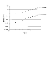
- FIG. 1 It is a schematic sectional drawing which illustrates the principal part of the organic EL element which concerns on 1 aspect of this invention. It is a schematic sectional drawing for demonstrating the manufacturing method of the organic EL element shown in FIG. It is a schematic sectional drawing for demonstrating the manufacturing method of the organic EL element shown in FIG. It is a schematic sectional drawing for demonstrating the manufacturing method of the organic EL element shown in FIG. 2 is a graph showing the relationship between the heating temperature after film formation of a 2-methyl-9,10-bis (naphthalen-2-yl) anthracene (MADN) film and the molecular orientation and current density in the heated MADN film. is there.
- FIG. 1 2-methyl-9,10-bis (naphthalen-2-yl) anthracene
- FIG. 2 is a view showing a stable structure of 2-methyl-9,10-bis (naphthalen-2-yl) anthracene (MADN).
- FIG. 2 is a diagram showing the molecular structure of 2-methyl-9,10-bis (naphthalen-2-yl) anthracene (MADN) and the HOMO distribution.
- FIG. 2 is a diagram showing the molecular structure and LUMO distribution of 2-methyl-9,10-bis (naphthalen-2-yl) anthracene (MADN).
- FIG. 2 is a view showing a stable structure of N, N′-di (naphthalen-1-yl) -N, N′-diphenyl-benzidine ( ⁇ -NPD).
- FIG. 2 is a diagram showing the molecular structure of N, N′-di (naphthalen-1-yl) -N, N′-diphenyl-benzidine ( ⁇ -NPD) and the HOMO distribution.
- FIG. 4 is a view showing a stable structure of 4,4 ′, 4 ′′ -tris (carbazol-9-yl) triphenylamine (TCTA).
- FIG. 3 is a diagram showing the molecular structure and HOMO distribution of 4,4 ′, 4 ′′ -tris (carbazol-9-yl) triphenylamine (TCTA).
- FIG. 3 is a view showing a stable structure of 2,9-dimethyl-4,7-diphenyl-1,10-phenanthroline (BCP).
- BCP 2,9-dimethyl-4,7-diphenyl-1,10-phenanthroline
- FIG. 2 is a diagram showing the molecular structure and LUMO distribution of 2,9-dimethyl-4,7-diphenyl-1,10-phenanthroline (BCP). It is a figure which shows the stable structure of N, N- dicarbazolyl-3,5-benzene (m-CP). It is a figure which shows the molecular structure and distribution of HOMO of N, N- dicarbazolyl-3,5-benzene (m-CP). It is a top view which illustrates the principal part of one Embodiment of the display apparatus provided with the organic EL element shown in FIG.
- FIG. 2 is an equivalent circuit diagram of one pixel illustrating a main part of an embodiment of a display device including the organic EL element shown in FIG. 1.
- FIG. 1 is an equivalent circuit diagram of one pixel illustrating a main part of an embodiment of a display device including the organic EL element shown in FIG. 1.
- FIG. 2 is a plan view of one pixel illustrating a main part of an embodiment of a display device including the organic EL element shown in FIG. 1.
- 3 is a schematic cross-sectional view illustrating the main part of the element of Example 1.
- FIG. 6 is a schematic cross-sectional view illustrating the main part of an element of Example 2.
- FIG. 6 is a graph showing measurement results of current-voltage characteristics for the elements of Example 2 and Comparative Example 2. It is a schematic sectional drawing explaining the method of confirming the lamination
- the organic electroluminescence (hereinafter sometimes abbreviated as “organic EL”) element includes a pair of electrodes on a base material, and has two or more layers of organic thin films between the pair of electrodes.
- Tg glass transition point
- the pair of electrodes function as an anode or a cathode, respectively.
- FIG. 1 is a schematic cross-sectional view illustrating the main part of the organic EL element according to this embodiment.
- a first electrode 12, an organic EL layer 13, and a second electrode 14 are laminated on a base material 11 in this order, and are roughly configured. That is, the organic EL element 1 includes a pair of electrodes including a first electrode 12 and a second electrode 14 and an organic EL layer 13 sandwiched between the pair of electrodes on a substrate 11. is there.
- the base material 11 As the base material 11, a glass substrate can be illustrated.
- the thickness of the base material 11 is preferably 0.1 mm to 3 mm.
- the first electrode 12 and the second electrode 14 function as an anode or a cathode, respectively.
- Cathode materials include alkali metals such as lithium, sodium, potassium, cesium, etc .; alkaline earth metals such as magnesium, calcium, barium; aluminum; copper; silicon; an alloy composed of two or more of these metals; one or more of these Examples include compounds other than alloys containing metals.
- lithium, cesium, calcium, barium, aluminum, sodium potassium alloy, cesium compound, magnesium alloy, barium compound, aluminum lithium alloy, aluminum copper alloy, and aluminum copper silicon alloy are preferable from the viewpoint of good stability.
- fluorine compounds can be exemplified as preferable examples.
- the cathode may be a plurality of layers in which layers made of two or more kinds of materials are laminated, and the number of layers at this time is not particularly limited.
- a preferable example of the cathode having a plurality of layers is one in which a calcium layer and an aluminum layer are laminated.
- ITO indium tin oxide
- IZO indium zinc oxide
- Cd 2 SnO 4 cadmium stannate
- zinc oxide copper iodide
- gold platinum Etc.
- the film thicknesses of the first electrode 12 and the second electrode 14 are each preferably 20 nm to 200 nm.
- the organic EL layer 13 has a hole injection layer 13a, a hole transport layer 13b, a light emitting layer 13c, a hole prevention layer 13d, from the first electrode 12 side serving as an anode to the second electrode 14 side serving as a cathode.
- the electron transport layer 13e and the electron injection layer 13f are laminated in this order, and are roughly configured.
- the hole injection layer 13a, the hole transport layer 13b, the light emitting layer 13c, the hole prevention layer 13d, the electron transport layer 13e, and the electron injection layer 13f may each have a single layer structure or a multilayer structure.
- the hole injection layer 13a efficiently injects holes from the first electrode 12.
- the hole transport layer 13b efficiently transports holes to the light emitting layer 13c.
- the electron transport layer 13e efficiently transports electrons to the light emitting layer 13c.
- the electron injection layer 13f efficiently injects electrons from the second electrode 14. These correspond to the carrier injecting and transporting layer.
- the hole injection layer 13a, the hole transport layer 13b, the light emitting layer 13c, the hole prevention layer 13d, the electron transport layer 13e, and the electron injection layer 13f may be any of an organic thin film and an inorganic thin film. Of these layers, at least two layers are organic thin films.
- the material of the hole injection layer 13a and the hole transport layer 13b may be a known material, and preferably an oxide such as vanadium oxide (V 2 O 5 ) or molybdenum oxide (MoO 3 ) or an inorganic p-type semiconductor.
- an oxide such as vanadium oxide (V 2 O 5 ) or molybdenum oxide (MoO 3 ) or an inorganic p-type semiconductor.
- the material of the hole injection layer 13a is preferably a material having a lower HOMO energy level than the material of the hole transport layer 13b from the viewpoint of more efficiently injecting and transporting holes from the anode. And as a material of the positive hole transport layer 13b, a thing with the mobility of a hole higher than the material of the positive hole injection layer 13a is preferable.
- the hole injection layer 13a and the hole transport layer 13b may optionally contain an additive (donor, acceptor, etc.). And in order to improve the injection
- the acceptor may be a known one, and may be either an inorganic material or an organic material.
- Preferred examples of the inorganic material include gold (Au), platinum (Pt), tungsten (W), iridium (Ir), phosphorus oxychloride (POCl 3 ), hexafluoroarsenate ion (AsF 6 ⁇ ), and chlorine.
- Au gold
- platinum Pt
- Ir iridium
- POCl 3 phosphorus oxychloride
- hexafluoroarsenate ion AsF 6 ⁇
- chlorine chlorine
- bromine (Br) bromine
- V 2 O 5 vanadium oxide
- MoO 3 molybdenum oxide
- Preferred examples of the organic material include 7,7,8,8, -tetracyanoquinodimethane (TCNQ), tetrafluorotetracyanoquinodimethane (TCNQF 4 ), tetracyanoethylene (TCNE), hexacyanobutadiene (HCNB). ), Compounds having a cyano group such as dicyclodicyanobenzoquinone (DDQ); compounds having a nitro group such as trinitrofluorenone (TNF), dinitrofluorenone (DNF); fluoranil; chloranil; bromanyl and the like.
- TCNQ dicyclodicyanobenzoquinone
- TNF trinitrofluorenone
- DNF dinitrofluorenone
- fluoranil chloranil; bromanyl and the like.
- the acceptor is preferably a compound having a cyano group because it has a higher effect of increasing the hole concentration.
- the film thickness of the hole injection layer 13a is preferably 1 nm to 500 nm.
- the thickness of the hole transport layer 13b is preferably 5 nm to 500 nm.
- the material of the light emitting layer (organic light emitting layer) 13c may be a known material, may be only an organic light emitting material, or may be a combination of a light emitting dopant and a host material, and optionally, a hole transport material or an electron transport material. , Additives (donors, acceptors, etc.) may be included. Each of the above materials may be dispersed in a polymer material (binding resin) or an inorganic material. From the viewpoint of luminous efficiency and durability, the material of the light emitting layer 13c is preferably a material in which a luminescent dopant is dispersed in a host material.
- the organic light emitting material can be classified into a low molecular light emitting material and a polymer light emitting material, and may be classified into a fluorescent material or a phosphorescent material.
- low molecular weight organic materials (including host materials) used for the light emitting layer (organic light emitting layer) 13c include aromatics such as 4,4′-bis (2,2′-diphenylvinyl) -biphenyl (DPVBi).
- Preferred examples of the polymer organic material used for the light emitting layer (organic light emitting layer) 13c include poly (2-decyloxy-1,4-phenylene) (DO-PPP), poly [2,5-bis- [2- ( N, N, N-triethylammonium) ethoxy] -1,4-phenyl-alt-1,4-phenyllene] dibromide (PPP-NEt 3+ ), poly [2- (2′-ethylhexyloxy) -5 Methoxy-1,4-phenylenevinylene] (MEH-PPV), poly [5-methoxy- (2-propanoxysulfonide) -1,4-phenylenevinylene] (MPS-PPV), poly [2,5- Polyphenylenevinylene derivatives such as bis- (hexyloxy) -1,4-phenylene- (1-cyanovinylene)] (CN-PPV); poly (9,9-dioctylfluorene
- the organic light emitting material is preferably a low molecular light emitting material, and a phosphorescent material having high luminous efficiency is preferable from the viewpoint of reducing power consumption.
- p-quaterphenyl 3,5,3,5 tetra-tert-butylsecphenyl, 3,5,3,5 tetra-tert-butyl-
- Illustrative examples include fluorescent materials such as p-quinckphenyl.
- a fluorescent light-emitting material such as a styryl derivative; bis [(4,6-difluorophenyl) -pyridinato-N, C2 ′] picolinate iridium (III) (FIrpic), bis (4 ′, 6 '-Difluorophenylpolydinato) tetrakis (1-pyrazolyl) borate iridium (III) (FIr6) and the like, and in the case of a green light emitting material, tris (2-phenylpyridinato) iridium (Ir (ppy) 3 ) Examples thereof include phosphorescent organic metal complexes.
- the film thickness of the light emitting layer 13c is preferably 5 nm to 500 nm.
- the material of the hole blocking layer 13d, the electron transport layer 13e, and the electron injection layer 13f may be a known material, and preferably an inorganic material that is an n-type semiconductor if it is a low molecular weight material; 1,3-bis [2- (2,2′-bipyridin-6-yl) -1,3,4-oxadiazo-5-yl] benzene (Bpy-OXD, Tg 102 ° C.), 1,3-bis (5- (4- ( tert-butyl) phenyl) -1,3,4-oxadiazol-2-yl) benzene (OXD7) and other oxadiazole derivatives; 3- (4-biphenyl) -4-phenyl-5-tert-butylphenyl -Triazole derivatives such as 1,2,4-triazole (TAZ); thiopyrazine dioxide derivatives; benzoquinone derivatives; naphthoquinone derivatives; anthr
- examples of the material of the electron injection layer 13f include fluorides such as lithium fluoride (LiF) and barium fluoride (BaF 2 ); oxides such as lithium oxide (Li 2 O) and the like.
- the material of the electron injection layer 13f is preferably a material having a higher LUMO energy level than the material of the electron transport layer 13e from the viewpoint of more efficiently injecting and transporting electrons from the cathode. And as a material of the electron carrying layer 13e, the thing whose electron mobility is higher than the material of the electron injection layer 13f is preferable.
- the electron transport layer 13e and the electron injection layer 13f may optionally contain an additive (donor, acceptor, etc.). And in order to improve electron transport and injection
- the donor may be a known one, and may be either an inorganic material or an organic material.
- Preferred examples of the inorganic material include alkali metals such as lithium, sodium, and potassium; alkaline earth metals such as magnesium and calcium; rare earth elements; aluminum (Al); silver (Ag); copper (Cu); ) Etc. can be illustrated.
- organic material examples include compounds having an aromatic tertiary amine skeleton, condensed polycyclic compounds which may have a substituent such as phenanthrene, pyrene, perylene, anthracene, tetracene and pentacene, tetrathiafulvalene ( TTF), dibenzofuran, phenothiazine, carbazole and the like.
- a substituent such as phenanthrene, pyrene, perylene, anthracene, tetracene and pentacene, tetrathiafulvalene ( TTF), dibenzofuran, phenothiazine, carbazole and the like.
- Examples of the compound having an aromatic tertiary amine skeleton include anilines; phenylenediamines; N, N, N ′, N′-tetraphenylbenzidine, N, N′-bis- (3-methylphenyl) -N, Benzidines such as N′-bis- (phenyl) -benzidine, N, N′-di (naphthalen-1-yl) -N, N′-diphenyl-benzidine; triphenylamine, 4,4′4 ′′ -tris (N, N-diphenyl-amino) -triphenylamine, 4,4′4 ′′ -tris (N-3-methylphenyl-N-phenyl-amino) -triphenylamine, 4,4′4 ′′ -tris ( Triphenylamines such as N- (1-naphthyl) -N-phenyl-amino) -triphenylamine; N, N′-di
- the condensed polycyclic compound has a substituent means that one or more hydrogen atoms in the condensed polycyclic compound are substituted with a group other than a hydrogen atom (substituent).
- the number of groups is not particularly limited, and all hydrogen atoms may be substituted with a substituent.
- the position of the substituent is not particularly limited. Examples of the substituent include an alkyl group having 1 to 10 carbon atoms, an alkoxy group having 1 to 10 carbon atoms, an alkenyl group having 2 to 10 carbon atoms, an alkenyloxy group having 2 to 10 carbon atoms, and an aryl having 6 to 15 carbon atoms.
- the alkyl group may be linear, branched or cyclic, and examples of the linear or branched alkyl group include a methyl group, an ethyl group, an n-propyl group, an isopropyl group, and an n-butyl group.
- the cyclic alkyl group may be monocyclic or polycyclic, cyclopropyl group, cyclobutyl group, cyclopentyl group, cyclohexyl group, cycloheptyl group, cyclooctyl group, cyclononyl group, cyclodecyl group, norbornyl group, isobornyl group.
- the alkoxy group include a monovalent group in which the alkyl group is bonded to an oxygen atom.
- Examples of the alkenyl group include those in which one single bond (C—C) between carbon atoms is substituted with a double bond (C ⁇ C) in the alkyl group having 2 to 10 carbon atoms.
- Examples of the alkenyloxy group include a monovalent group in which the alkenyl group is bonded to an oxygen atom.
- the aryl group may be monocyclic or polycyclic, and the number of ring members is not particularly limited, and preferred examples include a phenyl group, a 1-naphthyl group, and a 2-naphthyl group.
- Examples of the aryloxy group include a monovalent group in which the aryl group is bonded to an oxygen atom.
- Examples of the halogen atom include a fluorine atom, a chlorine atom, a bromine atom, and an iodine atom.
- the donor is preferably a compound having an aromatic tertiary amine skeleton, a condensed polycyclic compound which may have a substituent, or an alkali metal because the effect of increasing the electron concentration is higher.
- the film thickness of the electron transport layer 13e is preferably 5 nm to 500 nm.
- the film thickness of the electron injection layer 13f is preferably 0.1 nm to 100 nm.
- the material constituting the organic thin film of two or more layers has a higher glass transition point (Tg) as the layer is closer to the base material 11. That is, the two or more layers of the organic thin film are arranged so that the higher the glass transition point of the material contained in the two or more layers of the organic thin film, the closer to the substrate.
- Tg glass transition point
- the two or more layers of the organic thin film are arranged so that the higher the glass transition point of the material contained in the two or more layers of the organic thin film, the closer to the substrate.
- a layer having a melting point close to the substrate 11 instead of the glass transition point The higher the one.
- a material having a glass transition point and a material having no glass transition point may be mixed.
- the glass transition point or the melting point is described above.
- the organic thin film satisfying the relationship is two layers or more. Although only two layers may be sufficient as the organic thin film satisfy
- Preferred embodiments include those satisfying the relationship of Tga>Tgb>Tgd>Tge> Tgf.
- the material constituting the organic thin film other than the light emitting material does not have a glass transition point or a glass transition point.
- the melting point of the layer closer to the substrate 11 may be higher.
- the light emitting layer 13c has an organic thin film (for example, it has the light emitting layer 13c as an organic thin film), and the glass transition point or melting
- the hole injection layer 13a, the hole transport layer 13b, the hole prevention layer 13d, the electron transport layer 13e, and the electron injection layer 13f are all organic thin films as described above, and the light emitting layer 13c is also an organic thin film.
- the glass transition point of the host material is Tgc, as a particularly preferred embodiment, one satisfying the relationship of Tga> Tgb> Tgc> Tgd> Tge> Tgf can be exemplified.
- the light emitting layer 13c has an organic thin film containing a host material and a light emitting material (for example, the light emitting layer 13c is an organic thin film).
- the electron transport layer 13e located above the light emitting layer 13c is an organic thin film.
- the host material constituting the light emitting layer 13c has a glass transition point or a melting point when it does not have a glass transition point. It is preferably higher than the glass transition point or melting point of the material constituting 13e.
- the difference in glass transition point or melting point of the materials constituting the organic thin films adjacent to each other is preferably 10 ° C. or higher.
- each layer which comprises an organic electroluminescent layer was demonstrated so far, for example, host material can be used also as a hole transport material or an electron transport material, and a hole transport material and an electron transport material are also hosts. Can be used as material.
- the organic EL element 1 can be manufactured by the following method, for example.
- 2A to 2C are schematic cross-sectional views for explaining a method for manufacturing the organic EL element 1.
- FIG. 2A the first electrode 12 is formed on the base material 11 by a sputtering method, a vacuum deposition method, or the like.
- the hole injection layer 13a, the hole transport layer 13b, the light emitting layer 13c, the hole prevention layer 13d, the electron transport layer 13e, and the electron injection layer 13f are arranged in this order on the first electrode 12.
- the organic EL layer 13 is formed by stacking. Each layer constituting the organic EL layer 13 can be formed by a known wet process, dry process, laser transfer method, or the like.
- a coating method such as a spin coating method, a dipping method, a doctor blade method, a discharge coating method, a spray coating method or the like using a liquid in which each material (material) constituting each layer is dissolved or dispersed in a solvent.
- a printing method such as an inkjet method, a relief printing method, an intaglio printing method, a screen printing method, or a micro gravure coating method can be exemplified.
- the liquid may contain additives for adjusting the physical properties of the liquid, such as a leveling agent and a viscosity modifier.
- resistance heating vapor deposition method electron beam (EB) vapor deposition method, molecular beam epitaxy (MBE) method, sputtering method, organic vapor deposition (OVPD) using each material (material) constituting each layer.
- EB electron beam
- MBE molecular beam epitaxy
- sputtering method organic vapor deposition
- OVPD organic vapor deposition
- the organic thin film having a glass transition point or a melting point of the constituent material has the above relationship, that is, two or more organic thin films other than the lowest layer are being formed.
- the glass transition point of the material constituting the organic thin film formed immediately before and in the temperature range of 20 ° C. to 20 ° C. higher than the glass transition point or melting point of the material constituting the organic thin film
- heat treatment is performed at a temperature lower than the melting point.
- the “two or more organic thin films” to be heat-treated are not necessarily continuous (in contact with each other), and an inorganic thin film or the like may be present therebetween.
- the organic thin film formed immediately before refers to the organic thin film positioned in the uppermost layer among the organic thin films positioned below the organic thin film to be heat-treated.
- the organic EL element 1 is well controlled in the orientation of the molecules constituting the organic thin film, regardless of whether the organic thin film is crystalline or amorphous.
- the injection efficiency and transport efficiency of carriers (electrons and holes) between the electrode and the organic thin film and between the organic thin films are improved, and the organic EL element 1 has a low driving voltage and low power consumption. .
- mixing of organic thin films and film roughness are suppressed, and the reliability and durability are excellent.
- the temperature lower than the glass transition point or the melting point of the material constituting the organic thin film formed immediately before is preferably 10 ° C. or lower than the glass transition point or the melting point.
- the material constituting the organic thin film is preferably a ⁇ -electron conjugated organic molecule. Thereby, the organic EL element 1 becomes further excellent in the said effect.
- the heat treatment is preferably performed under an inert gas atmosphere or under reduced pressure.
- the inert gas may be a known gas such as nitrogen gas, helium gas, or argon gas.
- the pressure when performing under reduced pressure is preferably 1 ⁇ 10 ⁇ 5 to 1 ⁇ 10 ⁇ 1 Pa.
- the organic thin film it is preferable to heat the organic thin film to be treated from the substrate 11 side. By doing in this way, the organic thin film by which the orientation was controlled better can be formed.
- the heat treatment may be performed by a known method, and may be any of a method of directly heating a heat source in contact with a heating target and a method of heating indirectly without contacting a heat source to the heating target.
- any heating method resistance heating, induction heating, microwave heating, infrared heating, arc heating, plasma heating, electron beam heating, ion beam heating, laser heating, or the like can be applied.
- An example is as follows. Using the following 2-methyl-9,10-bis (naphthalen-2-yl) anthracene (MADN, Tg 120 ° C.) as a molecule constituting the organic thin film, on a 120 nm thick IZO film on a glass substrate, A single layer thin film (MADN film) having a film thickness of 100 nm was formed by vacuum deposition, and this was heat-treated at a predetermined temperature (heating temperature) for 30 minutes.
- membrane was evaluated, the current density in the applied voltage 2V of a MADN film
- the results are shown in FIG.
- the two-dot chain line indicates S in the x direction of the anthracene skeleton.
- the solid line indicates S in the y direction of the anthracene skeleton.
- the broken line indicates the current density of the MADN film at an applied voltage of 2V.
- the evaluation of the molecular orientation state was performed by calculating the value of the orientation parameter S.
- the orientation parameter S is a value that quantifies the orientation direction of molecules in the thin film formed on the substrate (see “Applied Physics Letters, 93, 2008, 173302”), and depends on the extinction coefficient k of the thin film. And represented by the following formula (A).
- FIG. 4A is a diagram showing a stable structure of MADN. More specifically, the x direction indicates the short axis direction of the anthracene skeleton in MADN, and the y direction indicates the long axis direction of the anthracene skeleton in MADN.
- the stable structure of MADN shown here is obtained by a non-empirical molecular orbital calculation method level B3LYP / 6-31G (d) using general-purpose quantum chemical calculation software Gaussian09W (manufactured by Gaussian).
- the MADN HOMO distribution obtained by an ab initio molecular orbital calculation method using Gaussian09W is shown in FIG. 4B, and the LUMO distribution is shown in FIG. 4C together with the molecular structure.
- a Hartree-Fock method As a calculation method at the time of creation and execution of an input file, a Hartree-Fock method, a density functional (DFT) method, an MP (Moller Pelset perturbation theory) method, and a CC (Coupled Cluster theory) method can be selected.
- the DFT method is adopted.
- HOMO and LUMO are calculated simultaneously with the calculation of the stable structure, and the distribution of HOMO and LUMO is visualized by Gaussian View.
- Gaussian 09W As general-purpose quantum chemical calculation software used in the ab initio molecular orbital calculation method, Gaussian series (including Gaussian 09W) manufactured by Gaussian, USA, MarcoModel manufactured by Schrodinger, Examples include Spartan manufactured by Wavefunction, ABINIT-MP / BioStation manufactured by Advanced Software, and Gaussian09 (Gaussian09W, Gaussian09M) is particularly preferable.
- the glass transition point of MADN is 120 ° C., whereas when the heating temperature of the substrate is 100 ° C. or higher, the current density increases under the same measurement conditions. This means that when the heating temperature is 100 ° C. or higher, the applied voltage for obtaining the same current density can be reduced. That is, the carrier mobility is increased by setting the lower limit value of the heating temperature to a temperature 20 ° C. lower than the glass transition point of MADN.
- the upper limit value of the temperature is 140 ° C., but at a temperature of 150 ° C. or higher, the MADN film becomes rough. That is, film roughness is suppressed by setting the upper limit of the heating temperature to a temperature 20 ° C. higher than the glass transition point of MADN.
- the carrier mobility is increased because the ⁇ -electron conjugate plane (xy plane in FIG. 4A) of the anthracene skeleton in MADN is oriented substantially parallel to the substrate surface.
- the ⁇ -electron conjugated surface is oriented substantially parallel to the substrate surface means not only the case where the ⁇ -electron conjugated surface is completely parallel to the substrate surface, but also the ⁇ -electron conjugated surface and the substrate surface. It indicates that the anthracene skeleton is oriented so that the angle formed by the material surface is less than 45 °.
- HOMO and LUMO of MADN are mainly present in the anthracene skeleton and hardly exist in the naphthalene skeleton. Therefore, the ⁇ -electron conjugated surface in which molecular orbitals involved in carrier movement (HOMO when the ⁇ -electron conjugated organic molecule has hole transportability, LUMO when electron transportability) is mainly distributed with respect to the substrate surface
- HOMO when the ⁇ -electron conjugated organic molecule has hole transportability
- LUMO when electron transportability is mainly distributed with respect to the substrate surface
- the overlap of orbits of ⁇ electrons involved in carrier movement increases, and the carrier mobility increases.
- HOMO or LUMO may be evenly distributed over a plurality of ⁇ electron conjugated surfaces. In this case, it is preferable to align the ⁇ -electron conjugated surface having the largest area substantially parallel to the substrate surface, thereby further improving carrier transportability.
- MADN is carrier transportability.
- this MADN film is transported by charge.
- the carrier transport property of the MADN film is improved, and the driving voltage of the organic EL element can be lowered.
- Preferred ⁇ -electron conjugated organic molecules in the present embodiment include benzene skeleton, naphthalene skeleton, anthracene skeleton, phenanthroline skeleton, benzofuran skeleton, benzodifuran skeleton, triazine skeleton, imidazole skeleton, benzimidazole skeleton, triazole skeleton, pyridine skeleton, oxadiazole.
- Examples thereof include those having a ⁇ -electron conjugated surface such as a skeleton and a carbazole skeleton.
- the second electrode 14 is then formed on the organic EL layer 13 by a vacuum deposition method or the like, as shown in FIG. 2C.
- the organic EL element 1 shown in FIG. 1 is obtained.
- the organic EL element according to the present embodiment is not limited to that shown in FIG. 1, and the organic EL layer 13 has two or more organic thin films, and the material constituting the organic thin film is a glass transition point or glass. When it does not have a transition point, the melting point of the layer closer to the substrate 11 only needs to be higher.
- a part of the structure of the organic EL element 1 may be changed as appropriate, such as an organic EL layer provided with a light emitting layer and a carrier transport layer, and the structure of the organic EL layer 13 is as follows. It can be illustrated. (1) An organic EL layer in which a hole transport layer and a light emitting layer are laminated in this order from the first electrode 12 side to the second electrode 14 side.
- An organic EL layer in which a hole injection layer, a hole transport layer, a light emitting layer, a hole prevention layer, and an electron transport layer are laminated in this order from the first electrode 12 side to the second electrode 14 side.
- Organic in which a hole injection layer, a hole transport layer, a light emitting layer, a hole prevention layer, an electron transport layer, and an electron injection layer are laminated in this order from the first electrode 12 side to the second electrode 14 side EL layer.
- the hole injection layer, the hole transport layer, the electron blocking layer, the light emitting layer, the hole blocking layer, the electron transport layer, and the electron injection layer are arranged in this order.
- Laminated organic EL layer From the first electrode 12 side to the second electrode 14 side, the hole injection layer, the hole transport layer, the electron blocking layer, the light emitting layer, the hole blocking layer, the electron transport layer, and the electron injection layer are arranged in this order.
- the electron blocking layer may be a known one for organic EL, may have a single layer structure or a multilayer structure, and may be either an organic thin film or an inorganic thin film. And when it is an organic thin film, it is preferable to make it have the relationship of said glass transition point or melting
- a light emitting layer has an organic thin film containing a host material and a light emitting material (for example, a light emitting layer as an organic thin film).
- a host material for example, a light emitting layer as an organic thin film.
- the host material constituting the light-emitting layer has a glass transition point, or a melting point if it does not have a glass transition point. It is preferable that the glass transition point or melting point of the material constituting
- the organic EL element according to the present embodiment functions as a light emitting element without the organic EL layer having a light emitting layer for confining carriers, the organic EL layer has two or more organic thin films, and these glasses.
- the transition point or melting point may satisfy the above relationship.
- Organic EL elements other than the organic EL element 1 as described above can also be manufactured by the same method as the organic EL element 1 by performing the same heat treatment on the organic thin film.
- the orientation of the heat-treated two or more layers of organic thin films is controlled, and the roughness of these organic thin films and the mixing between adjacent organic thin films are suppressed. Therefore, carrier mobility becomes high, it is not necessary to apply a high voltage, power consumption is small, and reliability and durability are excellent. This is the same even if the organic thin film is amorphous. Therefore, the organic EL element according to the present embodiment prevents, for example, an interelectrode short circuit. This eliminates the need for multilayering or thickening of the organic thin film, which has conventionally been taken as a preventive measure, so that the organic EL device according to this embodiment can be manufactured easily and at low cost.
- the organic EL element which concerns on this embodiment, the following is mentioned as a method of confirming whether the organic thin film layer is formed in the desired lamination order, and each layer has a desired glass transition point.
- the organic EL element is polished obliquely as shown in FIG. Elemental analysis is performed for each layer of the exposed cross section to identify the material. By measuring the glass transition temperature of these materials, it is possible to confirm whether the organic thin film layers are formed in a desired stacking order and whether each layer has a desired glass transition point.
- the organic EL element is polished obliquely as shown in FIG. While this organic EL element is overheated, the exposed cross section is observed using a microscope or the like, and the state of the organic thin film layer is confirmed, whereby the glass transition temperature and the stacking order thereof can be confirmed.
- ⁇ -electron conjugated organic molecules other than MADN will be exemplified among materials suitable for the material constituting the organic thin film to which the present embodiment is applied.
- the ⁇ -electron conjugated organic molecules are not limited to those exemplified here.
- N, N′-di (naphthalen-1-yl) -N, N′-diphenyl-benzidine was determined by the level B3LYP / 6-31G of ab initio molecular orbital calculation using Gaussian09W.
- FIG. 5A shows the stable structure
- FIG. 5B shows the molecular structure and the HOMO distribution obtained by the above calculation method.
- ⁇ -NPD is suitable as a material for the hole transport layer or the hole injection layer
- HOMO involved in hole transport is mainly distributed in the biphenyl skeleton near the center
- HOMO in the naphthalene skeleton is slight. .
- ⁇ -NPD when ⁇ -NPD is used for forming a hole transport layer or a hole injection layer, ⁇ ⁇ NPD is formed so that the ⁇ -electron conjugate plane of the biphenyl skeleton, not the naphthalene skeleton, is substantially parallel to the substrate surface. It is considered that the carrier mobility can be increased by orienting the -NPD.
- Fig. 4 shows the stable structure of the following 4,4 ', 4 "-tris (carbazol-9-yl) triphenylamine (TCTA) determined by the level B3LYP / 6-31G of the ab initio molecular orbital calculation method using Gaussian09W.
- FIG. 6A shows the molecular structure and the HOMO distribution obtained by the above calculation method, respectively.
- TCTA hole transporting
- HOMO involved in hole transport is distributed throughout the molecule.
- the carbazole skeleton has the widest ⁇ -electron conjugated surface, at least one ⁇ -electron conjugate of the carbazole skeleton is present. It is considered that the carrier mobility can be increased by orienting the TCTA so that the surface is substantially parallel to the substrate surface.
- FIG. 7A shows the stable structure of 2,9-dimethyl-4,7-diphenyl-1,10-phenanthroline (BCP) shown below determined by the level B3LYP / 6-31G of the ab initio molecular orbital calculation method using Gaussian09W.
- FIG. 7B shows the molecular structure and LUMO distribution obtained by the above calculation method.
- BCP is suitable as a material for the electron transport layer or the electron injection layer, and LUMO involved in electron transport is mainly distributed in the phenanthroline skeleton.
- BCP when BCP is used for forming an electron transport layer or an electron injection layer, carrier transfer is achieved by orienting the BCP so that the ⁇ -electron conjugate plane of the phenanthroline skeleton is substantially parallel to the substrate surface. It is thought that the degree can be increased.
- m-CP N, N-dicarbazolyl-3,5-benzene
- FIG. 8A The stable structure of the following N, N-dicarbazolyl-3,5-benzene (m-CP) is shown in FIG. 8A, and the molecular structure and HOMO distribution are shown in FIG. 8B.
- m-CP is suitable as a material for a hole transport layer, a hole injection layer, or a light emitting layer (host material), and HOMO involved in hole transport is mainly distributed in the carbazole skeleton. Therefore, it is considered that the carrier mobility can be increased by orienting m-CP so that the ⁇ -electron conjugate plane of the carbazole skeleton is substantially parallel to the substrate surface.
- TAPC 4,4 ′-(cyclohexane-1,1-diyl) bis (N, N-di-p-tolylaniline)
- TAPC 4,4 ′-(cyclohexane-1,1-diyl) bis
- Each benzene skeleton has a ⁇ -electron conjugated surface, each ⁇ -electron conjugated surface is hexagonal or circular, and HOMO involved in hole transport is mainly distributed in the benzene skeleton bonded to the cyclohexane skeleton. ing. Therefore, it is considered that the carrier mobility can be increased by orienting the TAPC so that the ⁇ -electron conjugate plane of the benzene skeleton is substantially parallel to the substrate surface.
- DPAS 2,2′-bis (N, N-diphenylamine) -9,9′-spirobifluorene
- ⁇ HOMO that has an electron conjugate plane and participates in hole transport is mainly distributed in the diphenylamine skeleton. Therefore, it is considered that the carrier mobility can be increased by orienting the DPAS so that the ⁇ -electron conjugate plane of the diphenylamine skeleton is substantially parallel to the substrate surface.
- N1, N1 ′-(biphenyl-4,4′-diyl) bis (N1-phenyl-N4, N4-di-m-tolylbenzene-1,4-diamine) (DNTPD) is used as the hole transport layer or positive layer. It is suitable as a material for the hole injection layer, and each benzene skeleton is not coplanar, and each benzene skeleton has a ⁇ -electron conjugate plane.
- HOMO spreads to four benzene skeletons (two phenylene groups constituting one biphenylene group and two phenylene groups not corresponding to the phenylene group) sandwiched between nitrogen atoms. Therefore, it is considered that the carrier mobility can be increased by orienting DNTPD so that the ⁇ -electron conjugate planes of these benzene skeletons are substantially parallel to the substrate surface.
- N3, N3 ′′ ′, N3 ′′ ′-tetra-p-tolyl- [1,1 ′: 2 ′, 1 ′′: 2 ′′, 1 ′′ ′-quarterphenyl] -3,3 ′′ ′-diamine BTPD) is suitable as a material for the hole transport layer or the hole injection layer, and each benzene skeleton is not coplanar, and each benzene skeleton has a ⁇ -electron conjugate plane.
- HOMO is mainly distributed in the benzene skeleton bonded to the nitrogen atom. Therefore, it is considered that carrier mobility can be increased by orienting BTPD so that the ⁇ -electron conjugate planes of these benzene skeletons are substantially parallel to the substrate surface.
- the following 4,4 ′-(diphenylsilanediyl) bis (N, N-di-p-tolylaniline) (DTASi) is suitable as a material for the hole transport layer or the hole injection layer, It has a ⁇ -electron conjugate plane.
- HOMO involved in hole transport is mainly distributed in the benzene skeleton bonded to the nitrogen atom. Therefore, it is considered that the carrier mobility can be increased by orienting DTASi so that the ⁇ -electron conjugate planes of these benzene skeletons are substantially parallel to the substrate surface.
- the following 2,2-bis (4-carbazol-9-ylphenyl) adamantine (Ad-Cz) is suitable as a material for the hole transport layer or the hole injection layer, and each carbazole skeleton and each benzene skeleton are Have separate non-parallel ⁇ -electron conjugate surfaces.
- HOMO involved in hole transport is mainly distributed in the carbazole skeleton. Therefore, it is considered that the carrier mobility can be increased by orienting Ad—Cz so that the ⁇ -electron conjugate plane of the carbazole skeleton is substantially parallel to the substrate surface.
- CBP 4,4′-bis (carbazol-9-yl) biphenyl
- each carbazole skeleton and each benzene skeleton have separate ⁇ -electron conjugate surfaces.
- Not all ⁇ -electron conjugate planes are parallel to each other.
- HOMO is mainly distributed in the carbazole skeleton. Therefore, it is considered that the hole mobility can be increased by orienting the CBP so that the ⁇ -electron conjugate plane of the carbazole skeleton is substantially parallel to the substrate surface.
- LUMO is mainly distributed in a biphenyl skeleton sandwiched between nitrogen atoms. Therefore, it is considered that the electron mobility can be increased by orienting the CBP so that the ⁇ -electron conjugate plane of the biphenyl skeleton is substantially parallel to the substrate surface.
- the following diphenyl-di (o-tolyl) silane (UGH1) is suitable as a material for the light emitting layer (host material), and each benzene skeleton has a ⁇ -electron conjugate plane that is not parallel to each other.
- HOMO is mainly distributed in a benzene skeleton having a methyl group (o-tolyl group). Therefore, it is considered that the hole mobility can be increased by orienting UGH1 so that the ⁇ -electron conjugate planes of these benzene skeletons are substantially parallel to the substrate surface.
- LUMO is mainly distributed in a benzene skeleton (phenyl group) having no methyl group. Therefore, it is considered that the electron mobility can be increased by orienting UGH1 so that the ⁇ -electron conjugate planes of these benzene skeletons are substantially parallel to the substrate surface.
- the following 1,4-bistriphenylsilylbenzene (UGH2) is suitable as a material for the light emitting layer (host material), and each benzene skeleton has a ⁇ -electron conjugate plane that is not parallel to each other.
- HOMO and LUMO are mainly distributed in a benzene skeleton sandwiched between silicon atoms. Therefore, it is considered that the carrier mobility can be increased by orienting UGH2 so that the ⁇ -electron conjugate plane of the benzene skeleton is substantially parallel to the substrate surface.
- the following 9,9 ′-(5- (triphenylsilyl) -1,3-phenylene) bis (9H-carbazole) (SimCP) is suitable as a material of the light emitting layer (host material), and each carbazole skeleton,
- the benzene skeletons have ⁇ -electron conjugate planes that are not separately parallel to each other.
- HOMO is mainly distributed in the carbazole skeleton. Therefore, it is considered that the hole mobility can be increased by aligning SimCP so that the ⁇ -electron conjugate plane of the carbazole skeleton is substantially parallel to the substrate surface.
- LUMO is mainly distributed in the central benzene skeleton (a benzene skeleton in which one triphenylsilyl group and two carbazolyl groups are bonded to each other). Therefore, it is considered that the electron mobility can be increased by orienting SimCP so that the ⁇ -electron conjugate plane of the benzene skeleton is substantially parallel to the substrate surface.
- the following bis (3,5-di (9H-carbazol-9-yl) phenyl) diphenylsilane (SimCP2) is suitable as a material for the light-emitting layer (host material), and each carbazole skeleton and each benzene skeleton are separated separately. ⁇ -electron conjugate surfaces that are not parallel to each other. HOMO is mainly distributed in the carbazole skeleton. Therefore, it is considered that hole mobility can be increased by orienting SimCP2 so that the ⁇ -electron conjugate plane of the carbazole skeleton is substantially parallel to the substrate surface.
- LUMO is mainly distributed in a benzene skeleton in which silicon atoms and nitrogen atoms are bonded together. Therefore, it is considered that the electron mobility can be increased by orienting SimCP2 so that the ⁇ -electron conjugate plane of the benzene skeleton is substantially parallel to the substrate surface.
- SPPO1 9,9-spirobifluoren-2-yl-diphenyl-phosphine oxide
- each benzene skeleton is a ⁇ -electron conjugate plane that is not parallel to each other.
- SPPO1 9,9-spirobifluoren-2-yl-diphenyl-phosphine oxide
- HOMO involved in hole transport is mainly distributed in the fluorene skeleton that is not bonded to the phosphorus atom. Therefore, it is considered that the hole mobility can be increased by orienting SPPO1 so that the ⁇ -electron conjugate plane of the fluorene skeleton is substantially parallel to the substrate surface.
- LUMO involved in electron transport is mainly distributed in the fluorene skeleton bonded to the phosphorus atom. Therefore, it is considered that the electron mobility can be increased by orienting SPPO1 so that the ⁇ -electron conjugate plane of the fluorene skeleton is substantially parallel to the substrate surface.
- the following propane-2,2′-diylbis (4,1-phenylene) dibenzoate (MMA1) is suitable as a material for the light emitting layer (host material), and each benzene skeleton is a ⁇ -electron conjugate plane that is not separately parallel to each other.
- Have HOMO is mainly distributed in a benzene skeleton bonded to oxygen atoms. Therefore, it is considered that the hole mobility can be increased by orienting MMA1 so that the ⁇ -electron conjugate plane of the benzene skeleton is substantially parallel to the substrate surface.
- LUMO is mainly distributed in the terminal benzene skeleton (benzene skeleton bonded to the carbonyl group). Therefore, it is considered that the electron mobility can be increased by orienting MMA1 so that the ⁇ -electron conjugate plane of the benzene skeleton is substantially parallel to the substrate surface.
- the following 9- (4-tert-butylphenyl) -3,6-bis (triphenylsilyl) -9H-carbazole (CzSi) is suitable as a material for the light emitting layer (host material), and includes a carbazole skeleton and other benzenes.
- the skeletons have ⁇ -electron conjugate surfaces that are not separately parallel to each other.
- HOMO and LUMO are mainly distributed in the carbazole skeleton. Therefore, it is considered that the carrier mobility can be increased by orienting CzSi so that the ⁇ -electron conjugate plane of the carbazole skeleton is substantially parallel to the substrate surface.
- the following 4,4′-bis (diphenylphosphine oxide) biphenyl (PO1) is suitable as a material for the light emitting layer (host material), and has two benzene skeletons near the center (two benzene skeletons constituting a biphenylene group). Are on the same plane, have one ⁇ -electron conjugate plane, and are not parallel to the ⁇ -electron conjugate plane of the other benzene skeleton. HOMO and LUMO are mainly distributed in the two benzene skeletons. Therefore, it is considered that the carrier mobility can be increased by orienting PO1 so that the ⁇ -electron conjugate planes of these two benzene skeletons are substantially parallel to the substrate surface.
- the following 2,2′-bis (4-carbazol-9-yl) phenyl) -biphenyl is suitable as a material for the light emitting layer (host material), and the carbazole skeleton on both ends and the four near the center
- the benzene skeletons are not coplanar and have ⁇ -electron conjugate surfaces that are not parallel to each other.
- HOMO is mainly distributed in the carbazole skeleton. Therefore, it is considered that the hole mobility can be increased by orienting the BCBP so that the ⁇ -electron conjugate plane of the carbazole skeleton is substantially parallel to the substrate surface.
- LUMO is mainly distributed in four benzene skeletons. Therefore, it is considered that the electron mobility can be increased by orienting the BCBP so that the ⁇ electron conjugate planes of these benzene skeletons are substantially parallel to the substrate surface.
- the following 2,8-bis (diphenylphosphoryl) dibenzo [b, d] thiophene (PPT) is suitable as a material for the light emitting layer (host material), and the dibenzothiophene skeleton and the benzene skeleton near the center are parallel to each other. And HOMO and LUMO are mainly distributed in the dibenzothiophene skeleton. Therefore, it is considered that the carrier mobility can be increased by orienting the PPT so that the ⁇ -electron conjugate plane of the dibenzothiophene skeleton is substantially parallel to the substrate surface.
- HM-A1 4- (diphenylphosphoyl) -N, N-diphenylaniline
- HM-A1 is suitable as a material for the light emitting layer (host material), and each benzene skeleton has a ⁇ -electron conjugate surface that is not separately parallel to each other.
- HOMO is mainly distributed in the N, N-diphenylaniline skeleton. Therefore, it is considered that the hole mobility can be increased by orienting HM-A1 so that the ⁇ -electron conjugate plane of the N, N-diphenylaniline skeleton is substantially parallel to the substrate surface.
- LUMO is mainly distributed in a benzene skeleton sandwiched between nitrogen atoms and phosphorus atoms. Therefore, it is considered that the electron mobility can be increased by orienting HM-A1 so that the ⁇ -electron conjugate plane of the benzene skeleton is substantially parallel to the substrate surface.
- CZBDF 9,9 ′-((2,6-diphenylbenzo [1,2-b: 4,5-b ′] difuran-3,7-diyl) bis (4,1-phenylene)) bis (9H-carbazole )
- CZBDF 9,9 ′-((2,6-diphenylbenzo [1,2-b: 4,5-b ′] difuran-3,7-diyl) bis (4,1-phenylene)) bis (9H-carbazole ) (CZBDF) is suitable as a material for the light-emitting layer (host material), and has a benzodifuran skeleton, carbazole skeletons on both ends, and other benzene skeletons that are not parallel to each other, and HOMO and LUMO are benzodifurans. Mainly distributed in the skeleton. Therefore, it is considered that the carrier mobility can be increased by orienting the CZBDF so that the ⁇ -electron conjugate
- the following 2,4-bis (phenoxy) -6- (3-methyldiphenylamino) -1,3,5-triazine (BPMT) is suitable as a material for the light emitting layer (host material), and includes a triazine skeleton, each benzene
- the skeleton has ⁇ -electron conjugate surfaces that are not parallel to each other.
- HOMO is mainly distributed in the diphenylamino skeleton. Therefore, it is considered that the hole mobility can be increased by orienting the BPMT so that the ⁇ -electron conjugate plane of the diphenylamino skeleton is substantially parallel to the substrate surface.
- LUMO is mainly distributed in a triazine skeleton and a benzene skeleton bonded to an oxygen atom. Therefore, it is considered that the electron mobility can be increased by orienting BPMT so that the ⁇ -electron conjugate planes of these triazine skeleton and benzene skeleton are substantially parallel to the substrate surface.
- TPBI (1-phenyl-1H-benzimidazole)
- TPBI 1,3,5-benztolyl-1H-benzimidazole
- Each benzimidazole skeleton and each benzene skeleton have ⁇ -electron conjugate planes that are not parallel to each other, and the LUMO involved in electron transport is mainly distributed in the benzene skeleton near the center (the benzene skeleton to which three benzimidazole skeletons are bonded) Therefore, it is considered that the carrier mobility can be increased by orienting TPBI so that the ⁇ -electron conjugate plane of the benzene skeleton is substantially parallel to the substrate surface.
- the following 3- (4-biphenyl) -4-phenyl-5-tert-butylphenyl-1,2,4-triazole (TAZ) is suitable as a material for the electron transport layer or the electron injection layer.
- the benzene skeleton has ⁇ -electron conjugate planes that are not parallel to each other, and LUMO involved in electron transport is mainly distributed among the two benzene skeletons constituting the biphenyl group that are bonded to the triazole skeleton. Therefore, it is considered that the carrier mobility can be increased by orienting TAZ so that the ⁇ -electron conjugate plane of the benzene skeleton is substantially parallel to the substrate surface.
- BPhen 4,7-diphenyl-1,10-phenanthroline
- LUMO involved in transport is mainly distributed in the phenanthroline skeleton. Therefore, it is considered that the carrier mobility can be increased by orienting BPhen so that the ⁇ -electron conjugate plane of the phenanthroline skeleton is substantially parallel to the substrate surface.
- the following diphenylbis (4- (pyridin-3-yl) phenyl) silane (DPPS) is suitable as a material for the electron transport layer or the electron injection layer, and each pyridine skeleton and each benzene skeleton are not parallel to each other.
- LUMO involved in electron transport is mainly distributed in the pyridine skeleton and the benzene skeleton bonded to the pyridine skeleton. Therefore, it is considered that the carrier mobility can be increased by orienting the DPPS so that the ⁇ -electron conjugate planes of the pyridine skeleton and the benzene skeleton are substantially parallel to the substrate surface.
- TmPyPB 1,3,5-tri [(3-pyridyl) -phen-3-yl] benzene
- LUMO which has a non-parallel ⁇ -electron conjugate plane and is involved in electron transport is mainly distributed in four benzene skeletons. Therefore, it is considered that the carrier mobility can be increased by orienting TmPyPB so that the ⁇ -electron conjugate planes of these benzene skeletons are substantially parallel to the substrate surface.
- TpPyPB 1,3,5-tri [(3-pyridyl) -phen-3-yl] benzene
- TpPyPB 1,3,5-tri [(3-pyridyl) -phen-3-yl] benzene
- LUMO which has a non-parallel ⁇ -electron conjugate plane and is involved in electron transport is mainly distributed in four benzene skeletons. Therefore, it is considered that the carrier mobility can be increased by orienting TpPyPB so that the ⁇ -electron conjugate planes of these benzene skeletons are substantially parallel to the substrate surface.
- Examples of the display device including the organic EL element include an image signal output unit, a driving unit, and a light emitting unit.
- the image signal output unit generates and outputs an image signal.
- the driving unit generates a current or a voltage based on the image signal.
- the light emitting unit is the organic EL element, and emits light by the generated current or voltage. And it can be set as the structure similar to the conventional display apparatus except having provided this organic EL element.
- Such a display device includes the organic EL element, so that power consumption is small.
- FIG. 9A to 9C are schematic views illustrating the main part of one embodiment of a display device including the organic EL element.
- FIG. 9A is a plan view illustrating the main part of an embodiment of a display device including the organic EL element shown in FIG.
- FIG. 9B is an equivalent circuit diagram of one pixel illustrating the main part of one embodiment of the display device including the organic EL element shown in FIG.
- FIG. 9C is a plan view of one pixel illustrating the main part of one embodiment of the display device including the organic EL element shown in FIG.
- the display device 5 ⁇ / b> A shown here is an organic EL display device using the organic EL element 1.
- a matrix in which a plurality of scanning lines (gate wirings) 50 and a plurality of signal lines (source wirings) 51 are arranged vertically and horizontally is formed, and one pixel is located near each intersection.
- a provided pixel array is formed.
- a scanning line driving circuit (gate driver) 55 connected to the scanning line 50 and a signal line driving circuit (source driver) 56 connected to the signal line 51 are arranged.
- the scanning line driving circuit 55 and the signal line driving circuit 56 are connected to a controller 57 for supplying an image signal such as a timing signal for displaying an image or an RGB luminance signal.
- a power supply circuit 59 for supplying a signal voltage to be applied to the line 51 is connected.
- the controller 57 is connected to an external processing device 58 for supplying a horizontal / vertical synchronizing signal and an image signal from the outside to the display device 5A.
- one pixel of the pixel array constituting the display device 5A includes a switching transistor 52 connected to the scanning line 50 and the signal line 51, a driving transistor 53 for driving the pixel, and a storage capacitor. 54, and a pixel portion made of the organic EL element 1 is connected to the driving transistor 53.
- the organic EL element 1 emits light by driving current or voltage.
- the switching transistor 52 and the driving transistor 53 can be configured by, for example, a transistor using general polycrystalline silicon as a semiconductor.
- the display device 5A is configured as described above.
- the organic EL element is not limited to that shown in FIG. 1, and any organic EL element according to this embodiment can be used.
- Example 1 The organic EL element 2 having the configuration shown in FIG. 10 was manufactured by the following procedure. 10, the same components as those of the organic EL element 1 shown in FIG. 1 are denoted by the same reference numerals as those in FIG. 1, and detailed description thereof is omitted. This is the same in the following.
- a substrate having a 120 nm thick IZO film (first electrode 12, anode) formed on a 0.7 mm thick glass substrate (base material 11) was washed with water and then ultrasonicated in an alkaline aqueous solution. Washing was carried out for 30 minutes, followed by washing with water, followed by ultrasonic washing with ultrapure water for 15 minutes and drying at 110 ° C. for 30 minutes.
- the obtained substrate was subjected to UV-ozone treatment in an air atmosphere using a UV ozone cleaner. Then, the substrate was set in a vacuum vapor deposition machine, and a molybdenum oxide (MoO 3 ) film (hole injection layer 13a) was formed on the IZO film to a thickness of 1 nm, and then 4,4 ′, 4 ′′ -tris ( A carbazol-9-yl) triphenylamine (TCTA, Tg 151 ° C.) film (hole injection layer 13a) is formed to a thickness of 20 nm, and a MADN (Tg 120 ° C.) film (hole transport layer 13b) is formed to a thickness of 20 nm.
- MoO 3 molybdenum oxide
- the substrate was set in a glove box and heat-treated at 135 ° C. for 30 minutes in a nitrogen atmosphere. Next, the obtained substrate was set in a vacuum vapor deposition machine, and tris (2-phenyl) at a concentration of 6% by mass in 4,4′-bis (carbazol-9-yl) biphenyl (CBP, host material, Tg 62 ° C.).
- a film doped with pyridinate) iridium (Ir (ppy) 3 , dopant) (light-emitting layer 13c) is formed on the MADN film with a thickness of 20 nm, and a TmPyPB (Tg 79 ° C.) film (electron transport layer 13e) was formed to a thickness of 40 nm.
- This substrate was set in a glove box and heat-treated at 85 ° C. for 30 minutes in a nitrogen atmosphere.
- the obtained substrate was set in a vacuum vapor deposition machine, a shadow mask was placed on the TmPyPB film of the substrate, a lithium fluoride (LiF) film (electron injection layer 13f) was formed to a thickness of 1 nm, and aluminum
- the (Al) film (second electrode 14, cathode) was formed to a thickness of 100 nm to form a cathode and a wiring.
- the organic EL element 2 was manufactured by sealing the obtained board
- reference numeral 23 denotes an organic EL layer.
- the hole injection layer 13a is collectively shown as having a two-layer structure in which a layer made of MoO 3 and a layer made of TCTA are stacked.
- the organic EL element 3 shown in FIG. 11 was manufactured by the following procedure.
- a substrate having a 120 nm thick IZO film (first electrode 12, anode) formed on a 0.7 mm thick glass substrate (base material 11) was washed with water and then ultrasonicated in an alkaline aqueous solution. Washing was carried out for 30 minutes, followed by washing with water, followed by ultrasonic washing with ultrapure water for 15 minutes and drying at 110 ° C. for 30 minutes.
- the obtained substrate was subjected to UV-ozone treatment in an air atmosphere using a UV ozone cleaner.
- the substrate was set in a vacuum vapor deposition machine, and a 2-methyl-9,10-bis (naphthalen-2-yl) anthracene (MADN, Tg 120 ° C.) film (hole transport layer 13b) was deposited on the IZO film to a thickness of 50 nm. A film was formed with a thickness. And this board
- MADN 2-methyl-9,10-bis (naphthalen-2-yl) anthracene
- the obtained substrate was set in a vacuum evaporation machine, and a 1,3,5-tri [(3-pyridyl) -phen-3-yl] benzene (TmPyPB, Tg 79 ° C.) film (electron transport layer) was formed on the MADN film. 13e) was deposited with a film thickness of 50 nm. And this board
- the obtained substrate was set in a vacuum vapor deposition machine, a shadow mask was placed on the TmPyPB film of the substrate, a lithium fluoride (LiF) film (electron injection layer 13f) was formed to a thickness of 1 nm, and aluminum
- the (Al) film (second electrode 14, cathode) was formed to a thickness of 100 nm to form a cathode and a wiring.
- the organic EL element 3 was manufactured by sealing the obtained board
- reference numeral 33 denotes an organic EL layer.
- the aspect of the present invention can be used for an organic device including an organic EL element.
Landscapes
- Physics & Mathematics (AREA)
- Optics & Photonics (AREA)
- Electroluminescent Light Sources (AREA)
Abstract
有機エレクトロルミネッセンス素子は、基材と、前記基材上に設けられた一対の電極と、前記一対の電極間に設けられた少なくとも二層の有機薄膜を有する有機エレクトロルミネッセンス層と、を備える。少なくとも二層の前記有機薄膜のうち、二層又はそれ以上の前記有機薄膜は、二層又はそれ以上の前記有機薄膜に含まれる材料のガラス転移点、又はガラス転移点を有していない場合には融点が高いほど、前記基材に近くなるように配置されている。
Description
本発明は、有機エレクトロルミネッセンス素子及びその製造方法に関する。
本願は、2011年8月1日に、日本に出願された特願2011-168595号に基づき優先権を主張し、その内容をここに援用する。
本願は、2011年8月1日に、日本に出願された特願2011-168595号に基づき優先権を主張し、その内容をここに援用する。
有機電荷移動(CT)錯体、導電性高分子、有機光伝導体(OPC)等の研究成果を基礎として、OLED(Organic Light Emitting Diode)等の有機デバイスについて、1990年代前半から活発に研究開発が展開されている。現在では、OLED等の有機デバイスがMP3プレーヤー、携帯電話として実用化される段階にまで至り、次世代フラットパネルディスプレイとして注目されている。
有機エレクトロルミネッセンス(有機EL)素子は、1965年にHelflichらによって、アントラセン単結晶に高電圧を印加して、青色のELが生じるのが発見されたときにまでさかのぼる。しかしながら、厚さ1mmに達する厚い単結晶を用いたため、この素子の駆動電圧は数百Vに達した。そのため、低電圧化を進めるために、単結晶から薄膜化への検討が進められ、数十Vの印加電圧にてEL発光を得ることができるようになった。しかしながら、発光層のみから構成される単層構造であるため、一つの材料に電子と正孔のキャリア注入、輸送及び再結合の全ての過程を坦わせており、素子設計の自由度が極めて低く、さらなる低駆動電圧化が困難であった。そこで、有機薄膜積層構造へ研究が展開され、トリフェニルジアミン系材料を正孔注入層として、アルミニウムキノリン錯体を電子輸送層(発光層)として用いた厚さ100nmの二層構造により、10V程度の印加電圧で1000cd/m2に達する発光輝度が得られるようになった。このような従来の有機EL素子では、積層構造を用いることは重要であり、有機薄膜の厚さは二層又は三層の総計で50nm~500nm前後となる。
従来の有機EL素子は、厚さが100nm程度の薄膜層に、100mV/cm程度の高電圧を印加するため、電極間ショートが起こり易い。高電圧を印加する理由は、有機層のキャリア移動度が小さいためであり、高移動度の有機層を形成できれば印加電圧を低減でき、消費電力を低減できる。現在の一般的な有機EL素子のキャリア輸送層の移動度は、10-5cm2/Vsec~10-3cm2/Vsecであり、非晶質(アモルファス)材料でも10-3cm2/Vsec程度が限界といわれている。なお、本明細書において「非晶質」とは、結晶性を有していないこと、すなわち、分子の高次構造において規則性が無いことを指す。近年では、π電子共役材料としてスチリル系化合物を用いた単層薄膜を基板上に形成し、加熱処理を行うことで得られる薄膜において、分子の配向が基板表面に対して水平方向が優先することが報告されている(非特許文献1及び2参照)。このように、非晶質材料でも分子の配向を制御できることが明らかとなり、さらに高いキャリア移動度の実現が期待されている。
有機EL素子では、これを構成する分子(有機分子、有機化合物)として高い平坦性を有する非晶質材料を用い、電極間のショートを抑えることが重要である。そして、有機EL素子における薄膜の積層構造において、ガラス転移点(Tg)が一番低い材料からなる薄膜に対して、ガラス転移点±20℃程度の温度で加熱処理することにより、この薄膜を緻密化及び安定化させ、有機EL素子の長寿命化をはかる技術が開示されている(特許文献1及び2参照)。
Organic Electronics 10(2009)127-137
Applied Physics Letters 93(2008)173302
しかし、特許文献1及び2に記載の方法では、ガラス転移点が一番低い材料からなる薄膜しか、緻密化及び安定化させることができず、複数の薄膜を同様に処理できない。そして、複数の薄膜を緻密化及び安定化させようとすると、ある薄膜においてはガラス転移点を大きく超える温度で加熱処理せざるを得なくなることがあり、この場合、この薄膜と隣接する(上層又は下層の)薄膜との間で混合層が生じたり、薄膜に荒れが生じたりする。このように従来の有機EL素子は、消費電力が小さくなく、信頼性及び耐久性に優れていなかった。
本発明の態様は上記事情に鑑みてなされたものであり、消費電力が小さく、信頼性及び耐久性に優れた有機EL素子を提供する。
本発明の一態様は、基材と、前記基材上に一対の電極と、前記一対の電極間に設けられた少なくとも二層の有機薄膜を有する有機エレクトロルミネッセンス層と、を備え、少なくとも二層の前記有機薄膜のうち、二層又はそれ以上の前記有機薄膜は、二層又はそれ以上の前記有機薄膜に含まれる材料のガラス転移点、又はガラス転移点を有していない場合には融点が高いほど、前記基材に近くなるよう配置されている有機エレクトロルミネッセンス素子を提供する。
また、本発明の一態様における有機エレクトロルミネッセンス素子において、二層又はそれ以上の前記有機薄膜はが発光層を含み、前記発光層が、ホスト材料及び発光材料を含み、二層又はそれ以上の前記有機薄膜は、前記発光材料以外の二層又はそれ以上の前記有機薄膜に含まれる材料のガラス転移点、又はガラス転移点を有していない場合には融点が高いほど、前記基材に近くなるよう配置されてもよい。
また、本発明の一態様における有機エレクトロルミネッセンス素子において、前記有機エレクトロルミネッセンス層が、二層又はそれ以上の前記有機薄膜として、発光層と電子輸送層とを含み、前記電子輸送層と前記基材との間に前記発光層が配置され、前記発光層が、ホスト材料及び発光材料を含み、前記ホスト材料のガラス転移点、又はガラス転移点を有していない場合には融点が、前記電子輸送層を構成する材料の前記ガラス転移点又は融点よりも高くてもよい。
また、本発明の一態様における有機エレクトロルミネッセンス素子において、前記有機エレクトロルミネッセンス層が、二層又はそれ以上の前記有機薄膜として、発光層と、正孔輸送層とを含み、前記正孔輸送層と前記基材との間に前記発光層が配置され、前記発光層が、ホスト材料及び発光材料を含み、前記ホスト材料のガラス転移点、又はガラス転移点を有していない場合には融点が、前記正孔輸送層を構成する材料の前記ガラス転移点又は融点よりも高くてもよい。
また、本発明の一態様における有機エレクトロルミネッセンス素子において、二層又はそれ以上の前記有機薄膜は、互いに隣接し、互いに隣接する二層又はそれ以上の前記有機薄膜は、前記有機薄膜を構成する材料の、前記ガラス転移点又は融点の差が、10℃以上であってもよい。
また、本発明の一態様における有機エレクトロルミネッセンス素子において、前記有機薄膜の少なくとも一つに含まれる材料が、π電子共役有機分子であってもよい。
また、本発明の他の態様は、基材上に一方の電極、有機エレクトロルミネッセンス層、及び他方の電極をこの順に積層を含み、前記有機エレクトロルミネッセンス層の形成は、少なくとも二層の有機薄膜を形成することを含み、少なくとも二層の前記有機薄膜のうち最下層以外が、その成膜中又は成膜後に、前記有機薄膜を構成する材料の前記ガラス転移点又は融点よりも20℃低い温度から20℃高い温度の温度域で、且つ直前に成膜した有機薄膜を構成する材料の前記ガラス転移点又は融点よりも低い温度で加熱処理される有機エレクトロルミネッセンス素子の製造方法を提供する。
また、本発明の他の態様における有機エレクトロルミネッセンス素子の製造方法において、前記有機エレクトロルミネッセンス層の形成は、前記有機薄膜のうち最下層以外が、その成膜中又は成膜後に、前記有機薄膜を構成する材料の前記ガラス転移点又は融点よりも20℃低い温度から20℃高い温度の温度域で、且つ直前に成膜した有機薄膜を構成する材料の前記ガラス転移点又は融点よりも10℃以上低い温度で加熱処理されてもよい。
また、本発明の一態様における有機エレクトロルミネッセンス素子において、二層又はそれ以上の前記有機薄膜はが発光層を含み、前記発光層が、ホスト材料及び発光材料を含み、二層又はそれ以上の前記有機薄膜は、前記発光材料以外の二層又はそれ以上の前記有機薄膜に含まれる材料のガラス転移点、又はガラス転移点を有していない場合には融点が高いほど、前記基材に近くなるよう配置されてもよい。
また、本発明の一態様における有機エレクトロルミネッセンス素子において、前記有機エレクトロルミネッセンス層が、二層又はそれ以上の前記有機薄膜として、発光層と電子輸送層とを含み、前記電子輸送層と前記基材との間に前記発光層が配置され、前記発光層が、ホスト材料及び発光材料を含み、前記ホスト材料のガラス転移点、又はガラス転移点を有していない場合には融点が、前記電子輸送層を構成する材料の前記ガラス転移点又は融点よりも高くてもよい。
また、本発明の一態様における有機エレクトロルミネッセンス素子において、前記有機エレクトロルミネッセンス層が、二層又はそれ以上の前記有機薄膜として、発光層と、正孔輸送層とを含み、前記正孔輸送層と前記基材との間に前記発光層が配置され、前記発光層が、ホスト材料及び発光材料を含み、前記ホスト材料のガラス転移点、又はガラス転移点を有していない場合には融点が、前記正孔輸送層を構成する材料の前記ガラス転移点又は融点よりも高くてもよい。
また、本発明の一態様における有機エレクトロルミネッセンス素子において、二層又はそれ以上の前記有機薄膜は、互いに隣接し、互いに隣接する二層又はそれ以上の前記有機薄膜は、前記有機薄膜を構成する材料の、前記ガラス転移点又は融点の差が、10℃以上であってもよい。
また、本発明の一態様における有機エレクトロルミネッセンス素子において、前記有機薄膜の少なくとも一つに含まれる材料が、π電子共役有機分子であってもよい。
また、本発明の他の態様は、基材上に一方の電極、有機エレクトロルミネッセンス層、及び他方の電極をこの順に積層を含み、前記有機エレクトロルミネッセンス層の形成は、少なくとも二層の有機薄膜を形成することを含み、少なくとも二層の前記有機薄膜のうち最下層以外が、その成膜中又は成膜後に、前記有機薄膜を構成する材料の前記ガラス転移点又は融点よりも20℃低い温度から20℃高い温度の温度域で、且つ直前に成膜した有機薄膜を構成する材料の前記ガラス転移点又は融点よりも低い温度で加熱処理される有機エレクトロルミネッセンス素子の製造方法を提供する。
また、本発明の他の態様における有機エレクトロルミネッセンス素子の製造方法において、前記有機エレクトロルミネッセンス層の形成は、前記有機薄膜のうち最下層以外が、その成膜中又は成膜後に、前記有機薄膜を構成する材料の前記ガラス転移点又は融点よりも20℃低い温度から20℃高い温度の温度域で、且つ直前に成膜した有機薄膜を構成する材料の前記ガラス転移点又は融点よりも10℃以上低い温度で加熱処理されてもよい。
本発明の態様によれば、消費電力が小さく、信頼性及び耐久性に優れた有機EL素子を提供できる。
<有機エレクトロルミネッセンス素子及びその製造方法>
本実施形態に係る有機エレクトロルミネッセンス(以下、「有機EL」と略記することがある)素子は、基材上に一対の電極を備え、前記一対の電極間に、二層以上の有機薄膜を有する有機EL層を備えた有機EL素子であって、二層又はそれ以上の前記有機薄膜を構成する材料は、ガラス転移点(以下、「Tg」と略記することがある)、又はガラス転移点を有していない場合には融点が、前記基材に近い層のものほど高い。前記一対の電極は、それぞれ陽極又は陰極として機能する。
本実施形態に係る有機エレクトロルミネッセンス(以下、「有機EL」と略記することがある)素子は、基材上に一対の電極を備え、前記一対の電極間に、二層以上の有機薄膜を有する有機EL層を備えた有機EL素子であって、二層又はそれ以上の前記有機薄膜を構成する材料は、ガラス転移点(以下、「Tg」と略記することがある)、又はガラス転移点を有していない場合には融点が、前記基材に近い層のものほど高い。前記一対の電極は、それぞれ陽極又は陰極として機能する。
図1は、本実施形態に係る有機EL素子の要部を例示する概略断面図である。
ここに示す有機EL素子1は、基材11上に、第一電極12、有機EL層13及び第二電極14がこの順に積層され、概略構成されている。すなわち、有機EL素子1は、基材11上に、第一電極12及び第二電極14からなる一対の電極と、前記一対の電極間に挟持された有機EL層13と、を備えたものである。
ここに示す有機EL素子1は、基材11上に、第一電極12、有機EL層13及び第二電極14がこの順に積層され、概略構成されている。すなわち、有機EL素子1は、基材11上に、第一電極12及び第二電極14からなる一対の電極と、前記一対の電極間に挟持された有機EL層13と、を備えたものである。
基材11としては、ガラス基板が例示できる。
基材11の厚さは、0.1mm~3mmであることが好ましい。
基材11の厚さは、0.1mm~3mmであることが好ましい。
第一電極12及び第二電極14は、それぞれ陽極又は陰極として機能する。
陰極の材質としては、リチウム、ナトリウム、カリウム、セシウム等のアルカリ金属;マグネシウム、カルシウム、バリウム等のアルカリ土類金属;アルミニウム;銅;ケイ素;二種以上のこれら金属からなる合金;一種以上のこれら金属を含む合金以外の化合物等が例示できる。なかでも、安定性が良好な点から、リチウム、セシウム、カルシウム、バリウム、アルミニウム、ナトリウムカリウム合金、セシウム化合物、マグネシウム合金、バリウム化合物、アルミニウムリチウム合金、アルミニウム銅合金、アルミニウム銅シリコン合金が好ましい。また、これら以外でも、好ましいものとしてフッ素化合物が例示できる。
陰極は、二種以上の材質からなる層が積層された複数層のものでもよく、この時の層数は特に限定されない。複数層の陰極で好ましいものとしては、カルシウム層及びアルミニウム層が積層されたものが例示できる。
陰極の材質としては、リチウム、ナトリウム、カリウム、セシウム等のアルカリ金属;マグネシウム、カルシウム、バリウム等のアルカリ土類金属;アルミニウム;銅;ケイ素;二種以上のこれら金属からなる合金;一種以上のこれら金属を含む合金以外の化合物等が例示できる。なかでも、安定性が良好な点から、リチウム、セシウム、カルシウム、バリウム、アルミニウム、ナトリウムカリウム合金、セシウム化合物、マグネシウム合金、バリウム化合物、アルミニウムリチウム合金、アルミニウム銅合金、アルミニウム銅シリコン合金が好ましい。また、これら以外でも、好ましいものとしてフッ素化合物が例示できる。
陰極は、二種以上の材質からなる層が積層された複数層のものでもよく、この時の層数は特に限定されない。複数層の陰極で好ましいものとしては、カルシウム層及びアルミニウム層が積層されたものが例示できる。
陽極の材質としては、酸化インジウムスズ(ITO)、酸化インジウム亜鉛(IZO(登録商標))、酸化インジウム、酸化スズ、カドミウムスタネート(Cd2SnO4)、酸化亜鉛、ヨウ化銅、金、白金等が例示できる。
第一電極12及び第二電極14の膜厚は、それぞれ20nm~200nmであることが好ましい。
有機EL層13は、陽極である第一電極12側から、陰極である第二電極14側へかけて、正孔注入層13a、正孔輸送層13b、発光層13c、正孔防止層13d、電子輸送層13e及び電子注入層13fがこの順に積層され、概略構成されている。
正孔注入層13a、正孔輸送層13b、発光層13c、正孔防止層13d、電子輸送層13e及び電子注入層13fは、それぞれ単層構造及び多層構造のいずれであってもよい。
正孔注入層13a、正孔輸送層13b、発光層13c、正孔防止層13d、電子輸送層13e及び電子注入層13fは、それぞれ単層構造及び多層構造のいずれであってもよい。
正孔注入層13aは、正孔の第一電極12からの注入を効率よく行うものである。
正孔輸送層13bは、正孔の発光層13cへの輸送を効率よく行うものである。
電子輸送層13eは、電子の発光層13cへの輸送を効率よく行うものである。
電子注入層13fは、電子の第二電極14からの注入を効率よく行うものである。
これらは、キャリア注入輸送層に該当する。
正孔輸送層13bは、正孔の発光層13cへの輸送を効率よく行うものである。
電子輸送層13eは、電子の発光層13cへの輸送を効率よく行うものである。
電子注入層13fは、電子の第二電極14からの注入を効率よく行うものである。
これらは、キャリア注入輸送層に該当する。
正孔注入層13a、正孔輸送層13b、発光層13c、正孔防止層13d、電子輸送層13e及び電子注入層13fは、有機薄膜及び無機薄膜のいずれでもよいが、これら各層を構成するすべての層のうち、少なくとも二層は有機薄膜である。
正孔注入層13a及び正孔輸送層13bの材質は、公知のものでよく、好ましいものとしては、酸化バナジウム(V2O5)、酸化モリブデン(MoO3)等の酸化物や無機p型半導体材料;ポルフィリン化合物、N,N’-ビス(3-メチルフェニル)-N,N’-ビス(フェニル)-ベンジジン(TPD)、N,N’-ジ(ナフタレン-1-イル)-N,N’-ジフェニル-ベンジジン(α-NPD)、4,4’,4”-トリス(カルバゾール-9-イル)トリフェニルアミン(TCTA、Tg151℃)、N,N-ジカルバゾリル-3,5-ベンゼン(m-CP、Tg55℃)、4,4’-(シクロヘキサン-1,1-ジイル)ビス(N,N-ジ-p-トリルアニリン)(TAPC)、2,2’-ビス(N,N-ジフェニルアミン)-9,9’-スピロビフルオレン(DPAS)、N1,N1’-(ビフェニル-4,4’-ジイル)ビス(N1-フェニル-N4,N4-ジ-m-トリルベンゼン-1,4-ジアミン)(DNTPD)、N3,N3,N3”’, N3”’-テトラ-p-トリル-[1,1’:2’,1”:2”,1”’-クオーターフェニル]-3,3”’-ジアミン(BTPD)、4,4’-(ジフェニルシランジイル)ビス(N,N-ジ-p-トリルアニリン)(DTASi)、2,2-ビス(4-カルバゾール-9-イルフェニル)アダマンティン(Ad-Cz)等の芳香族第三級アミン化合物;ヒドラゾン化合物、キナクリドン化合物、スチリルアミン化合物等の低分子含窒素化合物;ポリアニリン(PANI)、ポリアニリン-樟脳スルホン酸(PANI-CSA)、3,4-ポリエチレンジオキシチオフェン/ポリスチレンサルフォネイト(PEDOT/PSS)、ポリ(トリフェニルアミン)誘導体(Poly-TPD)、ポリビニルカルバゾール(PVCz)、ポリ(p-フェニレンビニレン)(PPV)、ポリ(p-ナフタレンビニレン)(PNV)等の高分子化合物;2-メチル-9,10-ビス(ナフタレン-2-イル)アントラセン(MADN、Tg120℃)等の芳香族炭化水素化合物等が例示できる。
正孔注入層13aの材質としては、陽極からの正孔の注入及び輸送をより効率よく行う観点から、正孔輸送層13bの材質よりも、HOMOのエネルギー準位が低い材質が好ましい。そして、正孔輸送層13bの材質としては、正孔注入層13aの材質よりも、正孔の移動度が高いものが好ましい。
正孔注入層13a及び正孔輸送層13bは、任意に添加剤(ドナー、アクセプター等)等を含んでいてもよい。
そして、正孔の注入性及び輸送性をより向上させるためには、正孔注入層13a及び正孔輸送層13bは、アクセプターを含むことが好ましい。
そして、正孔の注入性及び輸送性をより向上させるためには、正孔注入層13a及び正孔輸送層13bは、アクセプターを含むことが好ましい。
前記アクセプターは、公知のものでよく、無機材料及び有機材料のいずれでもよい。
前記無機材料の好ましいものとしては、金(Au)、白金(Pt)、タングステン(W)、イリジウム(Ir)、オキシ塩化リン(POCl3)、六フッ化ヒ酸イオン(AsF6 -)、塩素(Cl)、臭素(Br)、ヨウ素(I)、酸化バナジウム(V2O5)、酸化モリブデン(MoO3)等が例示できる。
前記有機材料の好ましいものとしては、7,7,8,8,-テトラシアノキノジメタン(TCNQ)、テトラフルオロテトラシアノキノジメタン(TCNQF4)、テトラシアノエチレン(TCNE)、ヘキサシアノブタジエン(HCNB)、ジシクロジシアノベンゾキノン(DDQ)等のシアノ基を有する化合物;トリニトロフルオレノン(TNF)、ジニトロフルオレノン(DNF)等のニトロ基を有する化合物;フルオラニル;クロラニル;ブロマニル等が例示できる。
前記無機材料の好ましいものとしては、金(Au)、白金(Pt)、タングステン(W)、イリジウム(Ir)、オキシ塩化リン(POCl3)、六フッ化ヒ酸イオン(AsF6 -)、塩素(Cl)、臭素(Br)、ヨウ素(I)、酸化バナジウム(V2O5)、酸化モリブデン(MoO3)等が例示できる。
前記有機材料の好ましいものとしては、7,7,8,8,-テトラシアノキノジメタン(TCNQ)、テトラフルオロテトラシアノキノジメタン(TCNQF4)、テトラシアノエチレン(TCNE)、ヘキサシアノブタジエン(HCNB)、ジシクロジシアノベンゾキノン(DDQ)等のシアノ基を有する化合物;トリニトロフルオレノン(TNF)、ジニトロフルオレノン(DNF)等のニトロ基を有する化合物;フルオラニル;クロラニル;ブロマニル等が例示できる。
前記アクセプターは、これらのなかでも、正孔濃度を増加させる効果がより高いことから、シアノ基を有する化合物が好ましい。
正孔注入層13aの膜厚は、1nm~500nmであることが好ましい。
正孔輸送層13bの膜厚は、5nm~500nmであることが好ましい。
正孔輸送層13bの膜厚は、5nm~500nmであることが好ましい。
発光層(有機発光層)13cの材質は、公知のものでよく、有機発光材料のみでもよいし、発光性のドーパントとホスト材料との組み合わせでもよく、さらに任意に正孔輸送材料、電子輸送材料、添加剤(ドナー、アクセプター等)等を含んでいてもよい。また、上記の各材料が高分子材料(結着用樹脂)又は無機材料中に分散されていてもよい。発光効率及び耐久性の観点からは、発光層13cの材質としては、ホスト材料中に発光性のドーパントが分散されたものが好ましい。
前記有機発光材料は、低分子発光材料及び高分子発光材料等に分類でき、蛍光材料又は燐光材料等に分類されるものでもよい。
発光層(有機発光層)13cに用いる低分子有機材料(ホスト材料を含む)の好ましいものとしては、4,4’-ビス(2,2’-ジフェニルビニル)-ビフェニル(DPVBi)等の芳香族ジメチリデン化合物;5-メチル-2-[2-[4-(5-メチル-2-ベンゾオキサゾリル)フェニル]ビニル]ベンゾオキサゾール等のオキサジアゾール化合物;3-(4-ビフェニル)-4-フェニル-5-t-ブチルフェニル-1,2,4-トリアゾール(TAZ)等のトリアゾール誘導体;1,4-ビス(2-メチルスチリル)ベンゼン等のスチリルベンゼン化合物;チオピラジンジオキシド誘導体、ベンゾキノン誘導体、ナフトキノン誘導体、アントラキノン誘導体、ジフェノキノン誘導体、フルオレノン誘導体等の蛍光性有機材料;アゾメチン亜鉛錯体、(8-ヒドロキシキノリナト)アルミニウム錯体(Alq3)等の蛍光発光有機金属錯体;BeBq(ビス(ベンゾキノリノラト)ベリリウム錯体);4,4’-ビス-(2,2-ジ-p-トリル-ビニル)-ビフェニル(DTVBi);トリス(1,3-ジフェニル-1,3-プロパンジオノ)(モノフェナントロリン)Eu(III)(Eu(DBM)3(Phen));ジフェニルエチレン誘導体;トリス[4-(9-フェニルフルオレン-9-イル)フェニル]アミン(TFTPA、Tg186℃)等のトリフェニルアミン誘導体;ジアミノカルバゾール誘導体;ビススチリル誘導体;芳香族ジアミン誘導体;キナクリドン系化合物;ペリレン系化合物;クマリン系化合物;ジスチリルアリーレン誘導体(DPVBi);オリゴチオフェン誘導体(BMA-3T);4,4’-ジ(トリフェニルシリル)-ビフェニル(BSB、Tg100℃)、ジフェニル-ジ(o-トリル)シラン(UGH1、Tg26℃)、1,4-ビストリフェニルシリルベンゼン(UGH2)、1,3-ビス(トリフェニルシリル)ベンゼン(UGH3、Tg46℃)、トリフェニル-(4-(9-フェニル-9H-フルオレン-9-イル)フェニル)シラン(TPSi-F、Tg100℃)等のシラン誘導体;9,9-ジ(4-ジカルバゾール-ベンジル)フルオレン(CPF)、3,6-ビス(トリフェニルシリル)カルバゾール(mCP)、4,4’-ビス(カルバゾール-9-イル)ビフェニル(CBP、Tg62℃)、4,4’-ビス(カルバゾール-9-イル)-2,2’-ジメチルビフェニル(CDBP、Tg111℃)、N,N-ジカルバゾリル-3,5-ベンゼン(m-CP、Tg55℃)、3-(ジフェニルホスホリル)-9-フェニル-9H-カルバゾール(PPO1、Tg74℃)、3,6-ジ(9-カルバゾリル)-9-(2-エチルヘキシル)カルバゾール(TCz1、Tg88℃)、9,9’-(5-(トリフェニルシリル)-1,3-フェニレン)ビス(9H-カルバゾール)(SimCP、Tg101℃)、ビス(3,5-ジ(9H-カルバゾール-9-イル)フェニル)ジフェニルシラン(SimCP2)、3-(ジフェニルホスホリル)-9-(4-ジフェニルホスホリル)フェニル)-9H-カルバゾール(PPO21、Tg111℃)、2,2-ビス(4-カルバゾリルフェニル)-1,1-ビフェニル(4CzPBP、Tg120℃)、3,6-ビス(ジフェニルホスホリル)-9-フェニル-9H-カルバゾール(PPO2、Tg123℃)、9-(4-tert-ブチルフェニル)-3,6-ビス(トリフェニルシリル)-9H-カルバゾール(CzSi、Tg131℃)、3,6-ビス[(3,5-ジフェニル)フェニル]-9-フェニル-カルバゾール(CzTP、Tg135℃)、9-(4-tert-ブチルフェニル)-3,6-ジトリチル-9H-カルバゾール(CzC、Tg167℃)、9-(4-tert-ブチルフェニル)-3,6-ビス(9-(4-メトキシフェニル)-9H-フルオレン-9-イル)-9H-カルバゾール(DFC、Tg180℃)、2,2’-ビス(4-カルバゾール-9-イル)フェニル)-ビフェニル(BCBP)、9,9’-((2,6-ジフェニルベンゾ[1,2-b:4,5-b’]ジフラン-3,7-ジイル)ビス(4,1-フェニレン))ビス(9H-カルバゾール)(CZBDF)等のカルバゾール誘導体;4-(ジフェニルフォスフォイル)-N,N-ジフェニルアニリン(HM-A1)等のアニリン誘導体;1,3-ビス(9-フェニル-9H-フルオレン-9-イル)ベンゼン(mDPFB)、1,4-ビス(9-フェニル-9H-フルオレン-9-イル)ベンゼン(pDPFB)、2,7-ビス(カルバゾール-9-イル)-9,9-ジメチルフルオレン(DMFL-CBP、Tg131℃)、2-[9,9-ジ(4-メチルフェニル)-フルオレン-2-イル]-9,9-ジ(4-メチルフェニル)フルオレン(BDAF、Tg153℃)、2-(9,9-スピロビフルオレン-2-イル)-9,9-スピロビフルオレン(BSBF、Tg176℃)、9,9-ビス[4-(ピレニル)フェニル]-9H-フルオレン(BPPF、Tg177℃)、2,2’-ジピレニル-9,9-スピロビフルオレン(Spiro-Pye、Tg189℃)、2,7-ジピレニル-9,9-スピロビフルオレン(2,2’-Spiro-Pye、Tg186℃)、2,7-ビス[9,9-ジ(4-メチルフェニル)-フルオレン-2-イル]-9,9-ジ(4-メチルフェニル)フルオレン(TDAF、Tg201℃)、2,7-ビス(9,9-スピロビフルオレン-2-イル)-9,9-スピロビフルオレン(TSBF、Tg231℃)、9,9-スピロビフルオレン-2-イル-ジフェニル-フォスフィンオキサイド(SPPO1)等のフルオレン誘導体;1,3-ジ(ピレン-1-イル)ベンゼン(m-Bpye、Tg97℃)等のピレン誘導体;プロパン-2,2’-ジイルビス(4,1-フェニレン)ジベンゾエート(MMA1)等のベンゾエート誘導体;4,4’-ビス(ジフェニルフォスフィンオキサイド)ビフェニル(PO1)、2,8-ビス(ジフェニルフォスフォリル)ジベンゾ[b,d]チオフェン(PPT)等のフォスフィンオキサイド誘導体;4,4”-ジ(トリフェニルシリル)-p-ターフェニル(BST、Tg113℃)等のターフェニル誘導体;2,4-ビス(フェノキシ)-6-(3-メチルジフェニルアミノ)-1,3,5-トリアジン(BPMT)等トリアジン誘導体が例示できる。
発光層(有機発光層)13cに用いる高分子有機材料の好ましいものとしては、ポリ(2-デシルオキシ-1,4-フェニレン)(DO-PPP)、ポリ[2,5-ビス-[2-(N,N,N-トリエチルアンモニウム)エトキシ]-1,4-フェニル-アルト-1,4-フェニルレン]ジブロマイド(PPP-NEt3+)、ポリ[2-(2’-エチルヘキシルオキシ)-5-メトキシ-1,4-フェニレンビニレン](MEH-PPV)、ポリ[5-メトキシ-(2-プロパノキシサルフォニド)-1,4-フェニレンビニレン](MPS-PPV)、ポリ[2,5-ビス-(ヘキシルオキシ)-1,4-フェニレン-(1-シアノビニレン)](CN-PPV)等のポリフェニレンビニレン誘導体;ポリ(9,9-ジオクチルフルオレン)(PDAF)等のポリスピロ誘導体;ポリ(N-ビニルカルバゾール)(PVK、Tg200℃)等のカルバゾール誘導体等が例示できる。
前記有機発光材料は、低分子発光材料が好ましく、低消費電力化の観点から、発光効率が高い燐光材料が好ましい。
前記発光性のドーパントの材質のうち、紫外発光材料であれば、p-クォーターフェニル、3,5,3,5テトラ-tert-ブチルセクシフェニル、3,5,3,5テトラ-tert-ブチル-p-クィンクフェニル等の蛍光発光材料等が例示できる。また、青色発光材料であれば、スチリル誘導体等の蛍光発光材料;ビス[(4,6-ジフルオロフェニル)-ピリジナト-N,C2’]ピコリネート イリジウム(III)(FIrpic)、ビス(4’,6’-ジフルオロフェニルポリジナト)テトラキス(1-ピラゾイル)ボレート イリジウム(III)(FIr6)等の、また、緑色発光材料であれば、トリス(2-フェニルピリジナート)イリジウム(Ir(ppy)3)等の燐光発光有機金属錯体等が例示できる。
発光層13cの膜厚は、5nm~500nmであることが好ましい。
正孔防止層13d、電子輸送層13e及び電子注入層13fの材質は、公知のものでよく、好ましいものとしては、低分子材料であれば、n型半導体である無機材料;1,3-ビス[2-(2,2’-ビピリジン-6-イル)-1,3,4-オキサジアゾ-5-イル]ベンゼン(Bpy-OXD、Tg102℃)、1,3-ビス(5-(4-(tert-ブチル)フェニル)-1,3,4-オキサジアゾールー2-イル)ベンゼン(OXD7)等のオキサジアゾール誘導体;3-(4-ビフェニル)-4-フェニル-5-tert-ブチルフェニル-1,2,4-トリアゾール(TAZ)等のトリアゾール誘導体;チオピラジンジオキシド誘導体;ベンゾキノン誘導体;ナフトキノン誘導体;アントラキノン誘導体;ジフェノキノン誘導体;フルオレノン誘導体;ベンゾジフラン誘導体;8-ヒドロキシキノリノラート-リチウム(Liq、Tg130℃)等のキノリン誘導体;2,7-ビス[2-(2,2’-ビピリジン-6-イル)-1,3,4-オキサジアゾ-5-イル]-9,9-ジメチルフルオレン(Bpy-FOXD、Tg134℃)等のフルオレン誘導体;1,3,5-トリ[(3-ピリジル)-フェン-3-イル]ベンゼン(TmPyPB、Tg79℃)、1,3,5-トリ[(3-ピリジル)-フェン-3-イル]ベンゼン(TpPyPB、Tg80℃)等のベンゼン誘導体;2,2’,2”-(1,3,5-ベンジントリイル)-トリス(1-フェニル-1-H-ベンゾイミダゾール)(TPBI、Tg122℃)等のベンゾイミダゾール誘導体;3,5-ジ(ピレン-1-イル)ピリジン(PY1、Tg107℃)等のピリジン誘導体;3,3’,5,5’-テトラ[(m-ピリジル)-フェン-3-イル]ビフェニル(BP4mPy、Tg107℃)等のビフェニル誘導体;4,7-ジフェニル-1,10-フェナントロリン(BPhen)、2,9-ジメチル-4,7-ジフェニル-1,10-フェナントロリン(BCP)等のフェナントロリン誘導体;トリス(2,4,6-トリメチル-3-(ピリジン-3-イル)フェニル)ボラン(3TPYMB)等のトリフェニルボラン誘導体;ジフェニルビス(4-(ピリジン-3-イル)フェニル)シラン(DPPS)等のテトラフェニルシラン誘導体が例示できる。また、高分子材料であれば、ポリ(オキサジアゾール)(Poly-OXZ)、ポリスチレン誘導体(PSS)等が例示できる。特に、電子注入層13fの材質としては、フッ化リチウム(LiF)、フッ化バリウム(BaF2)等のフッ化物;酸化リチウム(Li2O)等の酸化物等が例示できる。
電子注入層13fの材質としては、陰極からの電子の注入及び輸送をより効率よく行う観点から、電子輸送層13eの材質よりも、LUMOのエネルギー準位が高い材質が好ましい。そして、電子輸送層13eの材質としては、電子注入層13fの材質よりも、電子の移動度が高いものが好ましい。
電子輸送層13e及び電子注入層13fは、任意に添加剤(ドナー、アクセプター等)等を含んでいてもよい。
そして、電子の輸送及び注入性をより向上させるためには、電子輸送層13e及び電子注入層13fは、ドナーを含むことが好ましい。
そして、電子の輸送及び注入性をより向上させるためには、電子輸送層13e及び電子注入層13fは、ドナーを含むことが好ましい。
前記ドナーは、公知のものでよく、無機材料及び有機材料のいずれでもよい。
前記無機材料の好ましいものとしては、リチウム、ナトリウム、カリウム等のアルカリ金属;マグネシウム、カルシウム等のアルカリ土類金属;希土類元素;アルミニウム(Al);銀(Ag);銅(Cu);インジウム(In)等が例示できる。
前記有機材料の好ましいものとしては、芳香族3級アミン骨格を有する化合物、フェナントレン、ピレン、ペリレン、アントラセン、テトラセン、ペンタセン等の置換基を有していてもよい縮合多環化合物、テトラチアフルバレン(TTF)類、ジベンゾフラン、フェノチアジン、カルバゾール等が例示できる。
前記無機材料の好ましいものとしては、リチウム、ナトリウム、カリウム等のアルカリ金属;マグネシウム、カルシウム等のアルカリ土類金属;希土類元素;アルミニウム(Al);銀(Ag);銅(Cu);インジウム(In)等が例示できる。
前記有機材料の好ましいものとしては、芳香族3級アミン骨格を有する化合物、フェナントレン、ピレン、ペリレン、アントラセン、テトラセン、ペンタセン等の置換基を有していてもよい縮合多環化合物、テトラチアフルバレン(TTF)類、ジベンゾフラン、フェノチアジン、カルバゾール等が例示できる。
前記芳香族3級アミン骨格を有する化合物としては、アニリン類;フェニレンジアミン類;N,N,N’,N’-テトラフェニルベンジジン、N,N’-ビス-(3-メチルフェニル)-N,N’-ビス-(フェニル)-ベンジジン、N,N’-ジ(ナフタレン-1-イル)-N,N’-ジフェニル-ベンジジン等のベンジジン類;トリフェニルアミン、4,4’4”-トリス(N,N-ジフェニル-アミノ)-トリフェニルアミン、4,4’4”-トリス(N-3-メチルフェニル-N-フェニル-アミノ)-トリフェニルアミン、4,4’4”-トリス(N-(1-ナフチル)-N-フェニル-アミノ)-トリフェニルアミン等のトリフェニルアミン類;N,N’-ジ-(4-メチル-フェニル)-N,N’-ジフェニル-1,4-フェニレンジアミンのトリフェニルジアミン類が例示できる。
前記縮合多環化合物が「置換基を有する」とは、前記縮合多環化合物中の一つ以上の水素原子が、水素原子以外の基(置換基)で置換されていることを指し、前記置換基の数は特に限定されず、すべての水素原子が置換基で置換されていてもよい。そして、置換基の位置も特に限定されない。
前記置換基としては、炭素数1~10のアルキル基、炭素数1~10のアルコキシ基、炭素数2~10のアルケニル基、炭素数2~10のアルケニルオキシ基、炭素数6~15のアリール基、炭素数6~15のアリールオキシ基、水酸基、ハロゲン原子等が例示できる。
前記アルキル基は、直鎖状、分岐鎖状及び環状のいずれでもよく、直鎖状又は分枝鎖状のアルキル基としては、メチル基、エチル基、n-プロピル基、イソプロピル基、n-ブチル基、イソブチル基、sec-ブチル基、tert-ブチル基、n-ペンチル基、イソペンチル基、ネオペンチル基、tert-ペンチル基、1-メチルブチル基、n-ヘキシル基、2-メチルペンチル基、3-メチルペンチル基、2,2-ジメチルブチル基、2,3-ジメチルブチル基、n-ヘプチル基、2-メチルヘキシル基、3-メチルヘキシル基、2,2-ジメチルペンチル基、2,3-ジメチルペンチル基、2,4-ジメチルペンチル基、3,3-ジメチルペンチル基、3-エチルペンチル基、2,2,3-トリメチルブチル基、n-オクチル基、イソオクチル基、ノニル基、デシル基が例示できる。
また、環状のアルキル基は、単環状及び多環状のいずれでも良く、シクロプロピル基、シクロブチル基、シクロペンチル基、シクロヘキシル基、シクロヘプチル基、シクロオクチル基、シクロノニル基、シクロデシル基、ノルボルニル基、イソボルニル基、1-アダマンチル基、2-アダマンチル基、トリシクロデシル基が例示できる。
前記アルコキシ基としては、前記アルキル基が酸素原子に結合した一価の基が例示できる。
前記アルケニル基としては、炭素数が2~10の前記アルキル基において、炭素原子間の一つの単結合(C-C)が二重結合(C=C)に置換されたものが例示できる。
前記アルケニルオキシ基としては、前記アルケニル基が酸素原子に結合した一価の基が例示できる。
前記アリール基は、単環状及び多環状のいずれでもよく、環員数は特に限定されず、好ましいものとしては、フェニル基、1-ナフチル基、2-ナフチル基が例示できる。
前記アリールオキシ基としては、前記アリール基が酸素原子に結合した一価の基が例示できる。
前記ハロゲン原子としては、フッ素原子、塩素原子、臭素原子、ヨウ素原子が例示できる。
前記置換基としては、炭素数1~10のアルキル基、炭素数1~10のアルコキシ基、炭素数2~10のアルケニル基、炭素数2~10のアルケニルオキシ基、炭素数6~15のアリール基、炭素数6~15のアリールオキシ基、水酸基、ハロゲン原子等が例示できる。
前記アルキル基は、直鎖状、分岐鎖状及び環状のいずれでもよく、直鎖状又は分枝鎖状のアルキル基としては、メチル基、エチル基、n-プロピル基、イソプロピル基、n-ブチル基、イソブチル基、sec-ブチル基、tert-ブチル基、n-ペンチル基、イソペンチル基、ネオペンチル基、tert-ペンチル基、1-メチルブチル基、n-ヘキシル基、2-メチルペンチル基、3-メチルペンチル基、2,2-ジメチルブチル基、2,3-ジメチルブチル基、n-ヘプチル基、2-メチルヘキシル基、3-メチルヘキシル基、2,2-ジメチルペンチル基、2,3-ジメチルペンチル基、2,4-ジメチルペンチル基、3,3-ジメチルペンチル基、3-エチルペンチル基、2,2,3-トリメチルブチル基、n-オクチル基、イソオクチル基、ノニル基、デシル基が例示できる。
また、環状のアルキル基は、単環状及び多環状のいずれでも良く、シクロプロピル基、シクロブチル基、シクロペンチル基、シクロヘキシル基、シクロヘプチル基、シクロオクチル基、シクロノニル基、シクロデシル基、ノルボルニル基、イソボルニル基、1-アダマンチル基、2-アダマンチル基、トリシクロデシル基が例示できる。
前記アルコキシ基としては、前記アルキル基が酸素原子に結合した一価の基が例示できる。
前記アルケニル基としては、炭素数が2~10の前記アルキル基において、炭素原子間の一つの単結合(C-C)が二重結合(C=C)に置換されたものが例示できる。
前記アルケニルオキシ基としては、前記アルケニル基が酸素原子に結合した一価の基が例示できる。
前記アリール基は、単環状及び多環状のいずれでもよく、環員数は特に限定されず、好ましいものとしては、フェニル基、1-ナフチル基、2-ナフチル基が例示できる。
前記アリールオキシ基としては、前記アリール基が酸素原子に結合した一価の基が例示できる。
前記ハロゲン原子としては、フッ素原子、塩素原子、臭素原子、ヨウ素原子が例示できる。
前記ドナーは、これらのなかでも、電子濃度を増加させる効果がより高いことから、芳香族3級アミン骨格を有する化合物、置換基を有していてもよい縮合多環化合物、アルカリ金属が好ましい。
電子輸送層13eの膜厚は、5nm~500nmであることが好ましい。
また、電子注入層13fの膜厚は、0.1nm~100nmであることが好ましい。
また、電子注入層13fの膜厚は、0.1nm~100nmであることが好ましい。
有機EL素子1においては、有機EL層13のうち、二層以上の有機薄膜を構成する材料は、基材11に近い層のものほどガラス転移点(Tg)が高い。すなわち、二層又はそれ以上の前記有機薄膜は、二層又はそれ以上の前記有機薄膜に含まれる材料のガラス転移点が高い層ほど、前記基材に近くなるように配置されている。有機EL素子1において、二層又はそれ以上の前記有機薄膜を構成する材料の少なくとも一つがガラス転移点を有していない場合には、ガラス転移点に代わって融点が、基材11に近い層のものほど高い。このように、有機薄膜を構成する前記材料としては、ガラス転移点を有しているものと有していないものとが混在していてよい。
例えば、有機EL素子1において、正孔注入層13a、正孔輸送層13b、正孔防止層13d、電子輸送層13e及び電子注入層13fがすべて有機薄膜である場合、ガラス転移点又は融点について上記の関係を満たす有機薄膜は、二層又はそれ以上である。ガラス転移点又は融点について上記の関係を満たす有機薄膜は、二層のみでもよいが、層数が多いほど好ましい。すべての有機薄膜が上記の関係を満たすことは、特に好ましい。例えば、正孔注入層13a、正孔輸送層13b、正孔防止層13d、電子輸送層13e及び電子注入層13fのガラス転移点が順にTga、Tgb、Tgd、Tge及びTgfであるとすると、特に好ましい実施形態としては、Tga>Tgb>Tgd>Tge>Tgfの関係を満たすものが例示できる。
例えば、有機EL素子1において、正孔注入層13a、正孔輸送層13b、正孔防止層13d、電子輸送層13e及び電子注入層13fがすべて有機薄膜である場合、ガラス転移点又は融点について上記の関係を満たす有機薄膜は、二層又はそれ以上である。ガラス転移点又は融点について上記の関係を満たす有機薄膜は、二層のみでもよいが、層数が多いほど好ましい。すべての有機薄膜が上記の関係を満たすことは、特に好ましい。例えば、正孔注入層13a、正孔輸送層13b、正孔防止層13d、電子輸送層13e及び電子注入層13fのガラス転移点が順にTga、Tgb、Tgd、Tge及びTgfであるとすると、特に好ましい実施形態としては、Tga>Tgb>Tgd>Tge>Tgfの関係を満たすものが例示できる。
有機EL素子1においては、発光層13cがホスト材料及び発光材料を含む場合、前記発光材料以外の前記有機薄膜を構成する材料は、ガラス転移点、又はガラス転移点を有していない場合には融点が、基材11に近い層のものほど高くてもよい。このような有機EL層13としては、発光層13cが有機薄膜を有し(例えば、有機薄膜として発光層13cを有し)、そのホスト材料のガラス転移点又は融点が、その他の有機薄膜を構成する材料のガラス転移点又は融点との間に、上記の関係を有するものが例示できる。例えば、正孔注入層13a、正孔輸送層13b、正孔防止層13d、電子輸送層13e及び電子注入層13fが、上記のようにすべて有機薄膜であり、発光層13cも有機薄膜であって、そのホスト材料のガラス転移点がTgcであるとすると、特に好ましい実施形態としては、Tga>Tgb>Tgc>Tgd>Tge>Tgfの関係を満たすものが例示できる。
また、発光層13cがホスト材料及び発光材料を含む有機薄膜を有し(例えば、有機薄膜として発光層13cを有し)、例えば、発光層13cよりも上層に位置する電子輸送層13eが有機薄膜を有する(例えば、有機薄膜として電子輸送層13eを有する)場合、発光層13cを構成する前記ホスト材料は、ガラス転移点、又はガラス転移点を有していない場合には融点が、電子輸送層13eを構成する材料のガラス転移点又は融点よりも高いことが好ましい。
有機EL層13において、互いに隣接する前記有機薄膜を構成する材料の、前記ガラス転移点又は融点の差は、10℃以上であることが好ましい。
なお、ここまで、有機EL層を構成する各層の材質(材料)について説明したが、例えば、ホスト材料は正孔輸送材料又は電子輸送材料としても使用でき、正孔輸送材料及び電子輸送材料もホスト材料として使用できる。
有機EL素子1は、例えば、以下の方法で製造できる。図2A~図2Cは、有機EL素子1の製造方法を説明するための概略断面図である。
まず、図2Aに示すように、基材11上に、スパッタリング法、真空蒸着法等により第一電極12を形成する。
まず、図2Aに示すように、基材11上に、スパッタリング法、真空蒸着法等により第一電極12を形成する。
次いで、図2Bに示すように、第一電極12上に、正孔注入層13a、正孔輸送層13b、発光層13c、正孔防止層13d、電子輸送層13e及び電子注入層13fをこの順に積層し、有機EL層13を形成する。これら有機EL層13を構成する各層は、公知のウエットプロセス、ドライプロセス、レーザ転写法等により形成できる。
前記ウエットプロセスとしては、各層を構成する上記の各材質(材料)を溶媒に溶解又は分散させた液体を用いるスピンコーティング法、ディッピング法、ドクターブレード法、吐出コート法、スプレーコート法等の塗布法;インクジェット法、凸版印刷法、凹版印刷法、スクリーン印刷法、マイクログラビアコート法等の印刷法が例示できる。前記液体は、レベリング剤、粘度調整剤等の、液体の物性を調整するための添加剤を含んでいてもよい。
前記ドライプロセスとしては、各層を構成する上記の各材質(材料)を用いる抵抗加熱蒸着法、電子線(EB)蒸着法、分子線エピタキシー(MBE)法、スパッタリング法、有機気相蒸着(OVPD)法等が例示できる。
前記ドライプロセスとしては、各層を構成する上記の各材質(材料)を用いる抵抗加熱蒸着法、電子線(EB)蒸着法、分子線エピタキシー(MBE)法、スパッタリング法、有機気相蒸着(OVPD)法等が例示できる。
有機EL層13の形成時には、構成する材料のガラス転移点又は融点が上記の関係を有する前記有機薄膜、すなわち二層又はそれ以上の前記有機薄膜のうち、最下層以外のものについて、成膜中又は成膜後に、前記有機薄膜を構成する材料のガラス転移点又は融点よりも20℃低い温度から20℃高い温度の温度域で、且つ直前に成膜した有機薄膜を構成する材料のガラス転移点又は融点よりも低い温度で加熱処理する。ここで、加熱処理する「二層以上の有機薄膜」は、必ずしも連続している(互いに接触している)必要性はなく、間に無機薄膜等が存在していてもよい。すなわち、「直前に成膜した有機薄膜」とは、加熱処理する有機薄膜よりも下層に位置する有機薄膜の中で最上層に位置するものを指す。
このような条件で加熱処理することにより、有機EL素子1は、有機薄膜が結晶性及び非晶質のいずれであっても、これを構成する分子の配向が良好に制御される。これにより、電極及び有機薄膜間、並びに有機薄膜間でのキャリア(電子、正孔)の注入効率及び輸送効率が向上し、有機EL素子1は、駆動電圧が低く、消費電力が小さいものとなる。また、有機薄膜の混合や膜荒れが抑制され、信頼性及び耐久性に優れたものとなる。
このような条件で加熱処理することにより、有機EL素子1は、有機薄膜が結晶性及び非晶質のいずれであっても、これを構成する分子の配向が良好に制御される。これにより、電極及び有機薄膜間、並びに有機薄膜間でのキャリア(電子、正孔)の注入効率及び輸送効率が向上し、有機EL素子1は、駆動電圧が低く、消費電力が小さいものとなる。また、有機薄膜の混合や膜荒れが抑制され、信頼性及び耐久性に優れたものとなる。
上記の、直前に成膜した有機薄膜を構成する材料のガラス転移点又は融点よりも低い温度は、該ガラス転移点又は融点よりも10℃以上低い温度であることが好ましい。このようにすることで、有機EL素子1は、上記効果にさらに優れたものとなる。
前記有機薄膜を構成する材料は、π電子共役有機分子であることが好ましい。これにより、有機EL素子1は、上記効果にさらに優れたものとなる。
前記加熱処理は、不活性ガス雰囲気下又は減圧下において行うことが好ましい。不活性ガスは、窒素ガス、ヘリウムガス、アルゴンガス等、公知のものでよい。また、減圧下で行う場合の圧力は1×10⁻⁵~1×10⁻¹Paであることが好ましい。
前記加熱処理時には、処理対象の有機薄膜を基材11側から加熱することが好ましい。
このようにすることで、配向性がより良好に制御された有機薄膜を形成できる。
このようにすることで、配向性がより良好に制御された有機薄膜を形成できる。
前記加熱処理は、公知の方法で行えばよく、加熱対象に熱源を接触させて直接加熱する方法、及び加熱対象に熱源を接触させずに間接的に加熱する方法のいずれでもよい。いずれの加熱方法でも、抵抗加熱、誘導加熱、マイクロ波加熱、赤外線加熱、アーク加熱、プラズマ加熱、電子ビーム加熱、イオンビーム加熱、レーザ加熱等が適用できる。
有機薄膜を加熱処理するときの、「有機薄膜を構成する材料のガラス転移点又は融点よりも20℃低い温度から20℃高い温度の温度域」という加熱温度は、有機薄膜における分子の配向状態及び電流密度との関係から求められたものである。一例を挙げると、以下の通りである。
有機薄膜を構成する分子として、下記2-メチル-9,10-ビス(ナフタレン-2-イル)アントラセン(MADN、Tg120℃)を用いて、ガラス基材上の厚さ120nmのIZO膜上に、真空蒸着法により膜厚100nmの単層薄膜(MADN膜)を成膜し、これを所定の温度(加熱温度)で30分間加熱処理した。そして、形成したMADN膜における分子(MADN)の配向状態を評価し、MADN膜の印加電圧2Vでの電流密度を測定し、これらの加熱温度との関係を調べた。結果を図3に示す。なお、図3において、二点鎖線は、アントラセン骨格のx方向におけるSを示す。実線は、アントラセン骨格のy方向におけるSを示す。破線は、MADN膜の印加電圧2Vでの電流密度を示す。
有機薄膜を構成する分子として、下記2-メチル-9,10-ビス(ナフタレン-2-イル)アントラセン(MADN、Tg120℃)を用いて、ガラス基材上の厚さ120nmのIZO膜上に、真空蒸着法により膜厚100nmの単層薄膜(MADN膜)を成膜し、これを所定の温度(加熱温度)で30分間加熱処理した。そして、形成したMADN膜における分子(MADN)の配向状態を評価し、MADN膜の印加電圧2Vでの電流密度を測定し、これらの加熱温度との関係を調べた。結果を図3に示す。なお、図3において、二点鎖線は、アントラセン骨格のx方向におけるSを示す。実線は、アントラセン骨格のy方向におけるSを示す。破線は、MADN膜の印加電圧2Vでの電流密度を示す。

なお、分子の配向状態の評価は、配向パラメータSの値を算出することで行った。配向パラメータSは、基材上に形成された薄膜中の分子の配向方向を定量化する値であり(「Applied Physics Letters,93,2008,173302」参照)、薄膜の消衰係数kに依存し、下記式(A)で表される。
S=3/2cos2θ-1/2=(kz-kxy)/(kz+2kxy) ・・・・(A)
(式中、θは分子の配向軸と、基材表面に対して垂直な方向との為す角度(°)であり、kxyは基材表面と平行な方向の消衰係数であり、kzは基材表面に対して垂直な方向の消衰係数である。)
薄膜が光学的異方性を有していない場合のSは0であり、薄膜中の分子の配向方向が基材表面に対して完全に水平方向(平行)である場合のSは-0.5である。消衰係数kは、分光エリプソメーターによる測定値から算出される。したがって、配向パラメータSが、-0.1~-0.5の範囲にあることは、有機薄膜中で、基材表面に対して水平方向(平行)に配向している有機分子の割合が高いことを示す。
S=3/2cos2θ-1/2=(kz-kxy)/(kz+2kxy) ・・・・(A)
(式中、θは分子の配向軸と、基材表面に対して垂直な方向との為す角度(°)であり、kxyは基材表面と平行な方向の消衰係数であり、kzは基材表面に対して垂直な方向の消衰係数である。)
薄膜が光学的異方性を有していない場合のSは0であり、薄膜中の分子の配向方向が基材表面に対して完全に水平方向(平行)である場合のSは-0.5である。消衰係数kは、分光エリプソメーターによる測定値から算出される。したがって、配向パラメータSが、-0.1~-0.5の範囲にあることは、有機薄膜中で、基材表面に対して水平方向(平行)に配向している有機分子の割合が高いことを示す。
また、図3中の「x」及び「y」は、図4Aに示すMADNにおける、互いに直交する三つの方向のうちの二つの方向である(残る一つの方向は「z」である)。図4Aは、MADNの安定構造を示す図である。より具体的には、x方向は、MADNにおけるアントラセン骨格の短軸方向を示し、y方向は、MADNにおけるアントラセン骨格の長軸方向を示す。ここに示すMADNの安定構造は、汎用の量子化学計算ソフトであるGaussian09W(Gaussian社製)を用いた非経験的分子軌道計算法のレベルB3LYP/6-31G(d)により求めたものである。また、この安定構造をもとに、Gaussian09Wを用いた非経験的分子軌道計算法で求めたMADNのHOMOの分布を図4Bに、LUMOの分布を図4Cに、それぞれ分子構造と共に示す。
Gaussian09Wを用いてπ電子共役有機分子のHOMO又はLUMOの分布を計算する場合、まず、チェックポイントファイルを指定し、分子モデルの初期座標、計算方法と基底関数、電荷とスピン多重度をそれぞれ入力してインプットファイルを作成し、計算を実行することにより、最適構造化を行い、π電子共役有機分子の安定構造を計算する。次いで、得られた安定構造に対して分子軌道を表示することにより、π電子共役有機分子のHOMO又はLUMOの分布を可視化することができる。
なお、インプットファイルの作成及び実行の際の計算方法としては、Hartree-Fock法、密度汎関数(DFT)法、MP(Moller Plesset perturbation theory)法、CC(Coupled Cluster theory)法が選択できるが、本明細書におけるGaussian09Wを用いた計算では、DFT法を採用している。また、Gaussian09Wを用いた場合、安定構造の計算と同時に、HOMO及びLUMOも計算されており、GaussianViewによりHOMO及びLUMOの分布を可視化している。
なお、インプットファイルの作成及び実行の際の計算方法としては、Hartree-Fock法、密度汎関数(DFT)法、MP(Moller Plesset perturbation theory)法、CC(Coupled Cluster theory)法が選択できるが、本明細書におけるGaussian09Wを用いた計算では、DFT法を採用している。また、Gaussian09Wを用いた場合、安定構造の計算と同時に、HOMO及びLUMOも計算されており、GaussianViewによりHOMO及びLUMOの分布を可視化している。
ここでは、Gaussian09Wを用いた場合について説明したが、非経験的分子軌道計算法で用いる汎用の量子化学計算ソフトとしては、米国Gaussian社製のGaussianシリーズ(Gaussian09Wを含む)、Schrodinger社製のMarcoModel、Wavefunction社製のSpartan、アドバンスソフト社製のABINIT-MP/BioStation等が例示でき、なかでも、Gaussian09(Gaussian09W、Gaussian09M)が好適である。
図3から明らかなように、MADNのガラス転移点が120℃であるのに対して、基材の加熱温度が100℃以上になると、同じ測定条件で電流密度が上昇する。これは、加熱温度が100℃以上になると、同じ電流密度を得るための印加電圧を低減できることを意味する。すなわち、加熱温度の下限値を、MADNのガラス転移点よりも20℃低い温度とすることで、キャリア移動度が高くなる。一方、図3では、温度の上限値が140℃となっているが、150℃以上の温度では、MADN膜に膜荒れが生じてしまう。すなわち、加熱温度の上限値を、MADNのガラス転移点よりも20℃高い温度とすることで、膜荒れが抑制される。
このように加熱処理することで、キャリア移動度が高くなるのは、MADNにおけるアントラセン骨格のπ電子共役面(図4Aにおけるx-y平面)が、基材表面に対して実質的に平行に配向することによると推測される。ここで、「π電子共役面が基材表面に対して実質的に平行に配向する」とは、π電子共役面が基材表面に完全に平行な場合だけでなく、π電子共役面と基材表面とがなす角度が45°未満となるように、アントラセン骨格が配向することを示す。
図4B及び図4Cに示すように、MADNのHOMO及びLUMOは、アントラセン骨格に主に存在し、ナフタレン骨格にはほとんど存在しない。したがって、キャリア移動に関与する分子軌道(π電子共役有機分子が正孔輸送性の場合にはHOMO、電子輸送性の場合はLUMO)が主に分布するπ電子共役面が、基材表面に対して実質的に平行となることにより、キャリア移動に関与するπ電子の軌道の重なりが大きくなり、キャリア移動度が高くなる。
なお、π電子共役有機分子には、複数のπ電子共役面に満遍なくHOMO又はLUMOが分布している場合もある。この場合には、最も面積が大きいπ電子共役面を基材表面に対して実質的に平行に配向させることが好ましく、これにより、キャリア輸送性をより向上させることができる。
なお、π電子共役有機分子には、複数のπ電子共役面に満遍なくHOMO又はLUMOが分布している場合もある。この場合には、最も面積が大きいπ電子共役面を基材表面に対して実質的に平行に配向させることが好ましく、これにより、キャリア輸送性をより向上させることができる。
MADNはキャリア輸送性である。このように、MADNの配向が制御されることで、後述するように有機EL素子の一対の電極間に配置された有機薄膜の構成材料としてMADNを適用した場合には、このMADN膜が電荷輸送層及び正孔輸送層のいずれであっても、MADN膜のキャリア輸送性が向上し、有機EL素子の駆動電圧を低電圧化できる。
ここでは、MADNについて説明したが、本実施形態においては、上記のように加熱温度の温度域を設定することで、MADN以外のπ電子共役有機分子についても同様の効果を奏すると考えられる。
本実施形態において好ましいπ電子共役有機分子としては、ベンゼン骨格、ナフタレン骨格、アントラセン骨格、フェナントロリン骨格、ベンゾフラン骨格、ベンゾジフラン骨格、トリアジン骨格、イミダゾール骨格、ベンゾイミダゾール骨格、トリアゾール骨格、ピリジン骨格、オキサジアゾール骨格、カルバゾール骨格等のπ電子共役面を有するものが例示できる。
有機EL層13を形成後は、次いで、図2Cに示すように、有機EL層13上に、真空蒸着法等により第二電極14を形成する。
上記工程を行うことで、図1に示す有機EL素子1が得られる。
上記工程を行うことで、図1に示す有機EL素子1が得られる。
本実施形態に係る有機EL素子は、図1に示すものに限定されず、有機EL層13が二層以上の有機薄膜を有し、前記有機薄膜を構成する材料は、ガラス転移点、又はガラス転移点を有していない場合には融点が、基材11に近い層のものほど高くなっていればよい。例えば、有機EL層が発光層とキャリア輸送層とを備えたもの等、有機EL素子1の構成の一部を適宜変更したものでもよく、有機EL層13の構成を以下のようにしたものが例示できる。
(1)第一電極12側から第二電極14側へかけて、正孔輸送層及び発光層がこの順に積層された有機EL層。
(2)第一電極12側から第二電極14側へかけて、発光層及び電子輸送層がこの順に積層された有機EL層。
(3)第一電極12側から第二電極14側へかけて、正孔輸送層、発光層及び電子輸送層がこの順に積層された有機EL層。
(4)第一電極12側から第二電極14側へかけて、正孔注入層、正孔輸送層、発光層及び電子輸送層がこの順に積層された有機EL層。
(5)第一電極12側から第二電極14側へかけて、正孔注入層、正孔輸送層、発光層、電子輸送層及び電子注入層がこの順に積層された有機EL層。
(6)第一電極12側から第二電極14側へかけて、正孔注入層、正孔輸送層、発光層、正孔防止層及び電子輸送層がこの順に積層された有機EL層。
(7)第一電極12側から第二電極14側へかけて、正孔注入層、正孔輸送層、発光層、正孔防止層、電子輸送層及び電子注入層がこの順に積層された有機EL層。
(8)第一電極12側から第二電極14側へかけて、正孔注入層、正孔輸送層、電子防止層、発光層、正孔防止層、電子輸送層及び電子注入層がこの順に積層された有機EL層。
(1)第一電極12側から第二電極14側へかけて、正孔輸送層及び発光層がこの順に積層された有機EL層。
(2)第一電極12側から第二電極14側へかけて、発光層及び電子輸送層がこの順に積層された有機EL層。
(3)第一電極12側から第二電極14側へかけて、正孔輸送層、発光層及び電子輸送層がこの順に積層された有機EL層。
(4)第一電極12側から第二電極14側へかけて、正孔注入層、正孔輸送層、発光層及び電子輸送層がこの順に積層された有機EL層。
(5)第一電極12側から第二電極14側へかけて、正孔注入層、正孔輸送層、発光層、電子輸送層及び電子注入層がこの順に積層された有機EL層。
(6)第一電極12側から第二電極14側へかけて、正孔注入層、正孔輸送層、発光層、正孔防止層及び電子輸送層がこの順に積層された有機EL層。
(7)第一電極12側から第二電極14側へかけて、正孔注入層、正孔輸送層、発光層、正孔防止層、電子輸送層及び電子注入層がこの順に積層された有機EL層。
(8)第一電極12側から第二電極14側へかけて、正孔注入層、正孔輸送層、電子防止層、発光層、正孔防止層、電子輸送層及び電子注入層がこの順に積層された有機EL層。
前記電子防止層は、有機EL用として公知のものでよく、単層構造及び多層構造のいずれであってもよく、有機薄膜及び無機薄膜のいずれでもよい。そして、有機薄膜である場合には、その他の有機薄膜と同様に、上記のガラス転移点又は融点の関係を有するようにすることが好ましい。
有機EL素子において、発光層がホスト材料及び発光材料を含む有機薄膜を有し(例えば、有機薄膜として発光層を有し)、例えば、発光層よりも上層に位置する正孔輸送層が有機薄膜を有する(例えば、有機薄膜として正孔輸送層を有する)場合、発光層を構成する前記ホスト材料は、ガラス転移点、又はガラス転移点を有していない場合には融点が、正孔輸送層を構成する材料のガラス転移点又は融点よりも高いことが好ましい。
さらに、本実施形態に係る有機EL素子は、有機EL層がキャリアを閉じ込めるための発光層を備えることなく発光素子として機能し、有機EL層が二層以上の有機薄膜を有し、これらのガラス転移点又は融点が上記の関係を満たすものであってもよい。
上記のような有機EL素子1以外の有機EL素子も、有機薄膜について同様の加熱処理を行うことで、有機EL素子1と同様の方法で製造できる。
本実施形態に係る有機EL素子は、加熱処理された二層以上の有機薄膜の配向性が制御され、且つこれら有機薄膜の荒れや隣接する有機薄膜間での混合が抑制される。そのため、キャリア移動度が高くなり、高電圧を印加する必要が無く、消費電力が少なく、信頼性及び耐久性にも優れる。これは、前記有機薄膜が非晶質であっても同様である。したがって、本実施形態に係る有機EL素子は、例えば、電極間ショートが防止される。これにより従来その防止策としてとられていた有機薄膜の多層化や厚膜化等の手段も不要なので、本実施形態に係る有機EL素子は、簡便に且つ低コストで製造できる。
なお、本実施形態に係る有機EL素子において、有機薄膜層が所望の積層順に形成されているか、および各層が所望のガラス転移点を有しているか、を確認する方法として、以下が挙げられる。まず、有機EL素子を、図13に示すよう斜めに研磨する。露出した断面の各層ごとの元素分析を行い、材料を同定する。これらの材料のガラス転移温度を測定することにより、有機薄膜層が所望の積層順に形成されているか、および各層が所望のガラス転移点を有しているかを確認することができる。
また、その他方法としては、以下が挙げられる。有機EL素子を、図13に示すよう斜めに研磨する。この有機EL素子を過熱しながら、露出した断面を、顕微鏡などを用いて観察し、有機薄膜層の状態を確認することにより、ガラス転移温度およびその積層順を確認することができる。
以下、本実施形態を適用する有機薄膜を構成する材料として好適なもののうち、MADN以外のπ電子共役有機分子の具体的構造を例示する。ただし、π電子共役有機分子はここに例示するものに限定されるものではない。
下記N,N’-ジ(ナフタレン-1-イル)-N,N’-ジフェニル-ベンジジン(α-NPD)について、Gaussian09Wを用いた非経験的分子軌道計算法のレベルB3LYP/6-31Gにより求めた安定構造を図5Aに、分子構造と前記計算法で求めたHOMOの分布を図5Bに、それぞれ示す。
α-NPDは、正孔輸送層又は正孔注入層の材質として好適であり、正孔輸送に関与するHOMOが中央付近のビフェニル骨格に主に分布しており、ナフタレン骨格におけるHOMOは僅かである。したがって、α-NPDを正孔輸送層又は正孔注入層の形成に用いる場合には、ナフタレン骨格ではなくビフェニル骨格のπ電子共役面が基板表面に対して実質的に平行となるように、α-NPDを配向させることで、キャリア移動度を高くできると考えられる。
α-NPDは、正孔輸送層又は正孔注入層の材質として好適であり、正孔輸送に関与するHOMOが中央付近のビフェニル骨格に主に分布しており、ナフタレン骨格におけるHOMOは僅かである。したがって、α-NPDを正孔輸送層又は正孔注入層の形成に用いる場合には、ナフタレン骨格ではなくビフェニル骨格のπ電子共役面が基板表面に対して実質的に平行となるように、α-NPDを配向させることで、キャリア移動度を高くできると考えられる。
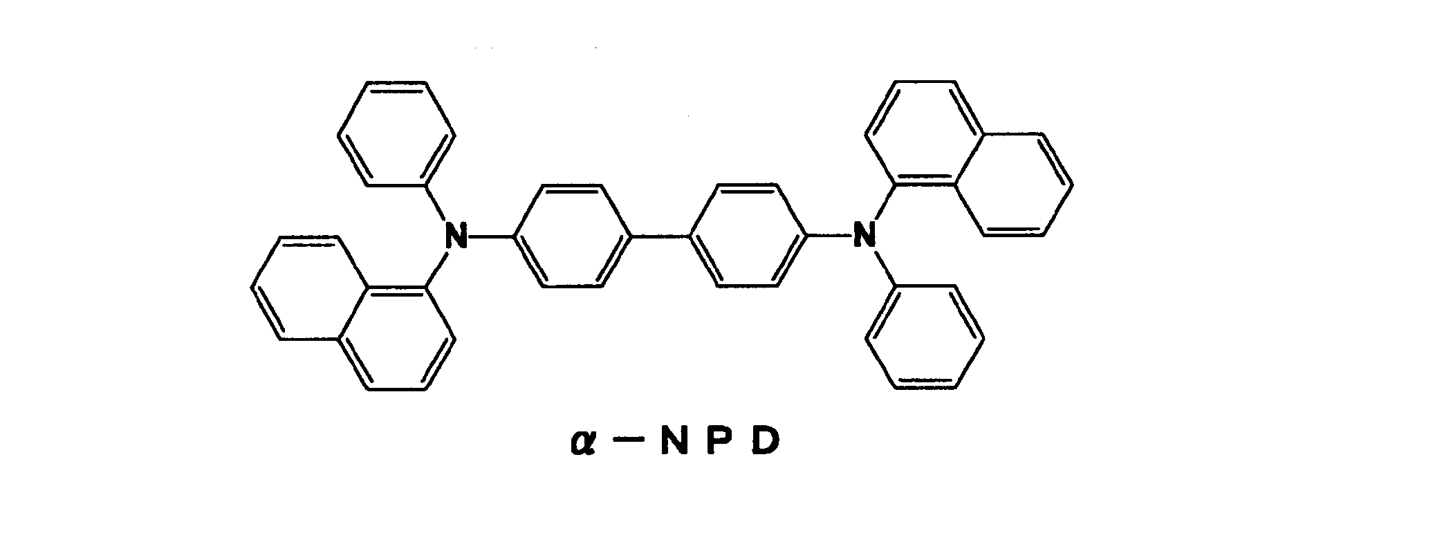
下記4,4’,4”-トリス(カルバゾール-9-イル)トリフェニルアミン(TCTA)について、Gaussian09Wを用いた非経験的分子軌道計算法のレベルB3LYP/6-31Gにより求めた安定構造を図6Aに、分子構造と前記計算法で求めたHOMOの分布を図6Bに、それぞれ示す。
正孔輸送性のTCTAは、正孔輸送に関与するHOMOが分子全体に分布しているが、カルバゾール骨格に最も面積の広いπ電子共役面を有するので、少なくともいずれかのカルバゾール骨格のπ電子共役面が基板表面に対して実質的に平行となるように、TCTAを配向させることで、キャリア移動度を高くできると考えられる。
正孔輸送性のTCTAは、正孔輸送に関与するHOMOが分子全体に分布しているが、カルバゾール骨格に最も面積の広いπ電子共役面を有するので、少なくともいずれかのカルバゾール骨格のπ電子共役面が基板表面に対して実質的に平行となるように、TCTAを配向させることで、キャリア移動度を高くできると考えられる。

下記2,9-ジメチル-4,7-ジフェニル-1,10-フェナントロリン(BCP)について、Gaussian09Wを用いた非経験的分子軌道計算法のレベルB3LYP/6-31Gにより求めた安定構造を図7Aに、分子構造と前記計算法で求めLUMOの分布を図7Bに、それぞれ示す。
BCPは、電子輸送層又は電子注入層の材質として好適であり、電子輸送に関与するLUMOがフェナントロリン骨格に主に分布している。したがって、BCPを電子輸送層又は電子注入層の形成に用いる場合には、フェナントロリン骨格のπ電子共役面が基板表面に対して実質的に平行となるように、BCPを配向させることで、キャリア移動度を高くできると考えられる。
BCPは、電子輸送層又は電子注入層の材質として好適であり、電子輸送に関与するLUMOがフェナントロリン骨格に主に分布している。したがって、BCPを電子輸送層又は電子注入層の形成に用いる場合には、フェナントロリン骨格のπ電子共役面が基板表面に対して実質的に平行となるように、BCPを配向させることで、キャリア移動度を高くできると考えられる。
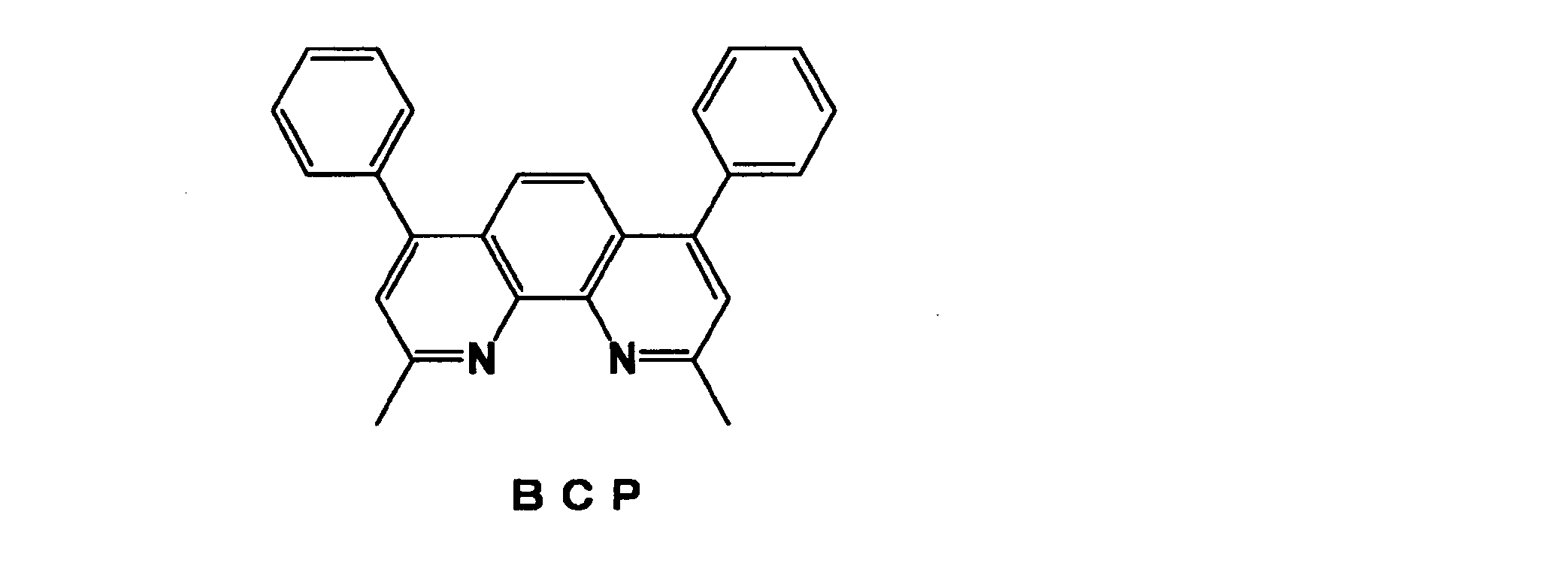
下記N,N-ジカルバゾリル-3,5-ベンゼン(m-CP)の安定構造を図8Aに、分子構造とHOMOの分布を図8Bに、それぞれ示す。
m-CPは、正孔輸送層、正孔注入層又は発光層(ホスト材料)の材質として好適であり、正孔輸送に関与するHOMOが、カルバゾール骨格に主に分布している。したがって、カルバゾール骨格のπ電子共役面が基板表面に対して実質的に平行となるように、m-CPを配向させることで、キャリア移動度を高くできると考えられる。
m-CPは、正孔輸送層、正孔注入層又は発光層(ホスト材料)の材質として好適であり、正孔輸送に関与するHOMOが、カルバゾール骨格に主に分布している。したがって、カルバゾール骨格のπ電子共役面が基板表面に対して実質的に平行となるように、m-CPを配向させることで、キャリア移動度を高くできると考えられる。

以下、同様に、Gaussian09Wを用いた非経験的分子軌道計算法のレベルB3LYP/6-31Gにより求めたHOMO及び/又はLUMOの分布と、分子の配向について説明する。
下記4,4’-(シクロヘキサン-1,1-ジイル)ビス(N,N-ジ-p-トリルアニリン)(TAPC)は、正孔輸送層又は正孔注入層の材質として好適であり、各ベンゼン骨格はそれぞれπ電子共役面を有し、各π電子共役面は6角形状又は円状になり、正孔輸送に関与するHOMOが、シクロヘキサン骨格に結合しているベンゼン骨格に主に分布している。したがって、前記ベンゼン骨格のπ電子共役面が基板表面に対して実質的に平行となるように、TAPCを配向させることで、キャリア移動度を高くできると考えられる。

下記2,2’-ビス(N,N-ジフェニルアミン)-9,9’-スピロビフルオレン(DPAS)は、正孔輸送層又は正孔注入層の材質として好適であり、各ベンゼン骨格はそれぞれπ電子共役面を有し、正孔輸送に関与するHOMOがジフェニルアミン骨格に主に分布している。したがって、ジフェニルアミン骨格のπ電子共役面が基板表面に対して実質的に平行となるように、DPASを配向させることで、キャリア移動度を高くできると考えられる。

下記N1,N1’-(ビフェニル-4,4’-ジイル)ビス(N1-フェニル-N4,N4-ジ-m-トリルベンゼン-1,4-ジアミン)(DNTPD)は、正孔輸送層又は正孔注入層の材質として好適であり、各ベンゼン骨格は同一平面状にはなく、各ベンゼン骨格はそれぞれπ電子共役面を有する。そして、HOMOが、窒素原子で挟まれた四つのベンゼン骨格(一つのビフェニレン基を構成する二つのフェニレン基、該フェニレン基に該当しない二つのフェニレン基)に広がっている。したがって、これらベンゼン骨格のπ電子共役面が基板表面に対して実質的に平行となるように、DNTPDを配向させることで、キャリア移動度を高くできると考えられる。

下記N3,N3,N3”’, N3”’-テトラ-p-トリル-[1,1’:2’,1”:2”,1”’-クオーターフェニル]-3,3”’-ジアミン(BTPD)は、正孔輸送層又は正孔注入層の材質として好適であり、各ベンゼン骨格は同一平面状にはなく、各ベンゼン骨格はそれぞれπ電子共役面を有する。そして、HOMOが、窒素原子に結合しているベンゼン骨格に主に分布している。したがって、これらベンゼン骨格のπ電子共役面が基板表面に対して実質的に平行となるように、BTPDを配向させることで、キャリア移動度を高くできると考えられる。

下記4,4’-(ジフェニルシランジイル)ビス(N,N-ジ-p-トリルアニリン)(DTASi)は、正孔輸送層又は正孔注入層の材質として好適であり、各ベンゼン骨格はそれぞれπ電子共役面を有する。そして、正孔輸送に関与するHOMOが、窒素原子に結合しているベンゼン骨格に主に分布している。したがって、これらベンゼン骨格のπ電子共役面が基板表面に対して実質的に平行となるように、DTASiを配向させることで、キャリア移動度を高くできると考えられる。

下記2,2-ビス(4-カルバゾール-9-イルフェニル)アダマンティン(Ad-Cz)は、正孔輸送層又は正孔注入層の材質として好適であり、各カルバゾール骨格、各ベンゼン骨格は、別々の互いに平行でないπ電子共役面を有する。そして、正孔輸送に関与するHOMOがカルバゾール骨格に主に分布している。したがって、カルバゾール骨格のπ電子共役面が基板表面に対して実質的に平行となるように、Ad-Czを配向させることで、キャリア移動度を高くできると考えられる。

下記4,4’-ビス(カルバゾール-9-イル)ビフェニル(CBP)は、発光層(ホスト材料)の材質として好適であり、各カルバゾール骨格、各ベンゼン骨格は、別々のπ電子共役面有し、全てのπ電子共役面が互いに平行ではない。そして、HOMOはカルバゾール骨格に主に分布している。したがって、カルバゾール骨格のπ電子共役面が基板表面に対して実質的に平行となるように、CBPを配向させることで、正孔移動度を高くできると考えられる。一方、LUMOは、窒素原子で挟まれたビフェニル骨格に主に分布している。したがって、前記ビフェニル骨格のπ電子共役面が基板表面に対して実質的に平行となるように、CBPを配向させることで、電子移動度を高くできると考えられる。

下記ジフェニル-ジ(o-トリル)シラン(UGH1)は、発光層(ホスト材料)の材質として好適であり、各ベンゼン骨格は、別々に互いに平行でないπ電子共役面を有する。そして、HOMOは、メチル基を有するベンゼン骨格(o-トリル基)に主に分布している。したがって、これらベンゼン骨格のπ電子共役面が基板表面に対して実質的に平行となるように、UGH1を配向させることで、正孔移動度を高くできると考えられる。一方、LUMOは、メチル基を有していないベンゼン骨格(フェニル基)に主に分布している。したがって、これらベンゼン骨格のπ電子共役面が基板表面に対して実質的に平行となるように、UGH1を配向させることで、電子移動度を高くできると考えられる。

下記1,4-ビストリフェニルシリルベンゼン(UGH2)は、発光層(ホスト材料)の材質として好適であり、各ベンゼン骨格は、別々に互いに平行でないπ電子共役面を有する。そして、HOMO及びLUMOは、ケイ素原子で挟まれたベンゼン骨格に主に分布している。したがって、前記ベンゼン骨格のπ電子共役面が基板表面に対して実質的に平行となるように、UGH2を配向させることで、キャリア移動度を高くできると考えられる。

下記9,9’-(5-(トリフェニルシリル)-1,3-フェニレン)ビス(9H-カルバゾール)(SimCP)は、発光層(ホスト材料)の材質として好適であり、各カルバゾール骨格、各ベンゼン骨格は、別々に互いに平行でないπ電子共役面を有する。そして、HOMOはカルバゾール骨格に主に分布している。したがって、カルバゾール骨格のπ電子共役面が基板表面に対して実質的に平行となるように、SimCPを配向させることで、正孔移動度を高くできると考えられる。一方、LUMOは、中央付近のベンゼン骨格(一つのトリフェニルシリル基、二つのカルバゾリル基がそれぞれ結合しているベンゼン骨格)に主に分布している。したがって、このベンゼン骨格のπ電子共役面が基板表面に対して実質的に平行となるように、SimCPを配向させることで、電子移動度を高くできると考えられる。

下記ビス(3,5-ジ(9H-カルバゾール-9-イル)フェニル)ジフェニルシラン(SimCP2)は、発光層(ホスト材料)の材質として好適であり、各カルバゾール骨格、各ベンゼン骨格は、別々に互いに平行でないπ電子共役面を有する。そして、HOMOはカルバゾール骨格に主に分布している。したがって、カルバゾール骨格のπ電子共役面が基板表面に対して実質的に平行となるように、SimCP2を配向させることで、正孔移動度を高くできると考えられる。一方、LUMOは、ケイ素原子及び窒素原子が共に結合しているベンゼン骨格に主に分布している。したがって、このベンゼン骨格のπ電子共役面が基板表面に対して実質的に平行となるように、SimCP2を配向させることで、電子移動度を高くできると考えられる。

下記9,9-スピロビフルオレン-2-イル-ジフェニル-フォスフィンオキサイド(SPPO1)は、発光層(ホスト材料)の材質として好適であり、各ベンゼン骨格は、別々に互いに平行でないπ電子共役面を有する。そして、正孔輸送に関与するHOMOが、リン原子に結合していない方のフルオレン骨格に主に分布している。したがって、このフルオレン骨格のπ電子共役面が基板表面に対して実質的に平行となるように、SPPO1を配向させることで、正孔移動度を高くできると考えられる。一方、電子輸送に関与するLUMOは、リン原子に結合している方のフルオレン骨格に主に分布している。したがって、このフルオレン骨格のπ電子共役面が基板表面に対して実質的に平行となるように、SPPO1を配向させることで、電子移動度を高くできると考えられる。

下記プロパン-2,2’-ジイルビス(4,1-フェニレン)ジベンゾエート(MMA1)は、発光層(ホスト材料)の材質として好適であり、各ベンゼン骨格は、別々に互いに平行でないπ電子共役面を有する。そして、HOMOは、酸素原子に結合したベンゼン骨格に主に分布している。したがって、このベンゼン骨格のπ電子共役面が基板表面に対して実質的に平行となるように、MMA1を配向させることで、正孔移動度を高くできると考えられる。一方、LUMOは、末端のベンゼン骨格(カルボニル基に結合しているベンゼン骨格)に主に分布している。したがって、このベンゼン骨格のπ電子共役面が基板表面に対して実質的に平行となるように、MMA1を配向させることで、電子移動度を高くできると考えられる。
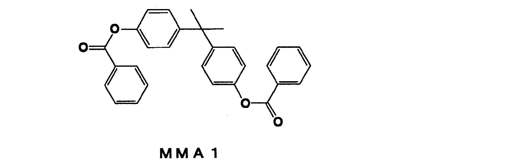
下記9-(4-tert-ブチルフェニル)-3,6-ビス(トリフェニルシリル)-9H-カルバゾール(CzSi)は、発光層(ホスト材料)の材質として好適であり、カルバゾール骨格、その他のベンゼン骨格は、別々に互いに平行でないπ電子共役面を有する。そして、HOMO及びLUMOがカルバゾール骨格に主に分布している。したがって、カルバゾール骨格のπ電子共役面が基板表面に対して実質的に平行となるように、CzSiを配向させることで、キャリア移動度を高くできると考えられる。
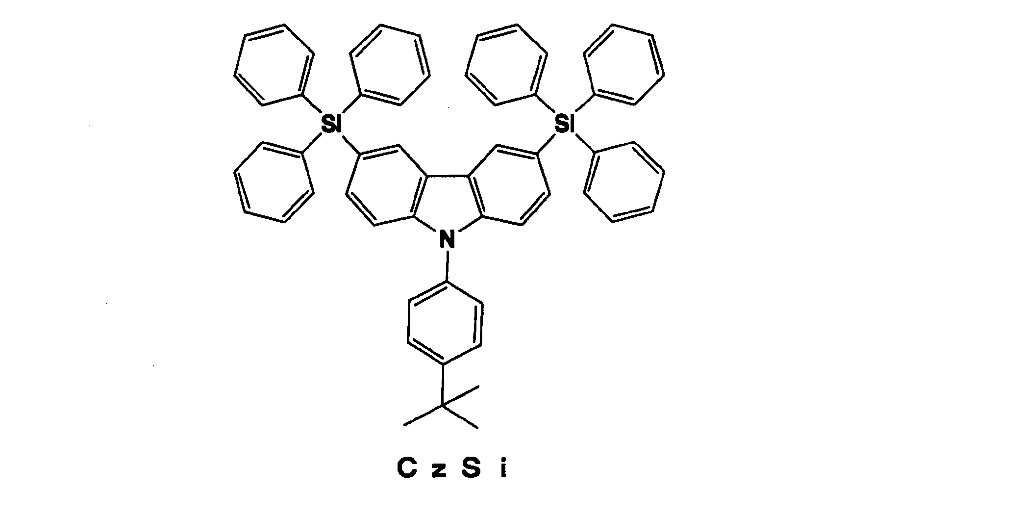
下記4,4’-ビス(ジフェニルフォスフィンオキサイド)ビフェニル(PO1)は、発光層(ホスト材料)の材質として好適であり、中央付近の二つのベンゼン骨格(ビフェニレン基を構成する二つのベンゼン骨格)が同一平面上にあり、一つのπ電子共役面を有し、その他のベンゼン骨格のπ電子共役面とは互いに平行でない。そして、HOMO及びLUMOが前記二つのベンゼン骨格に主に分布している。したがって、これら二つのベンゼン骨格のπ電子共役面が基板表面に対して実質的に平行となるように、PO1を配向させることで、キャリア移動度を高くできると考えられる。
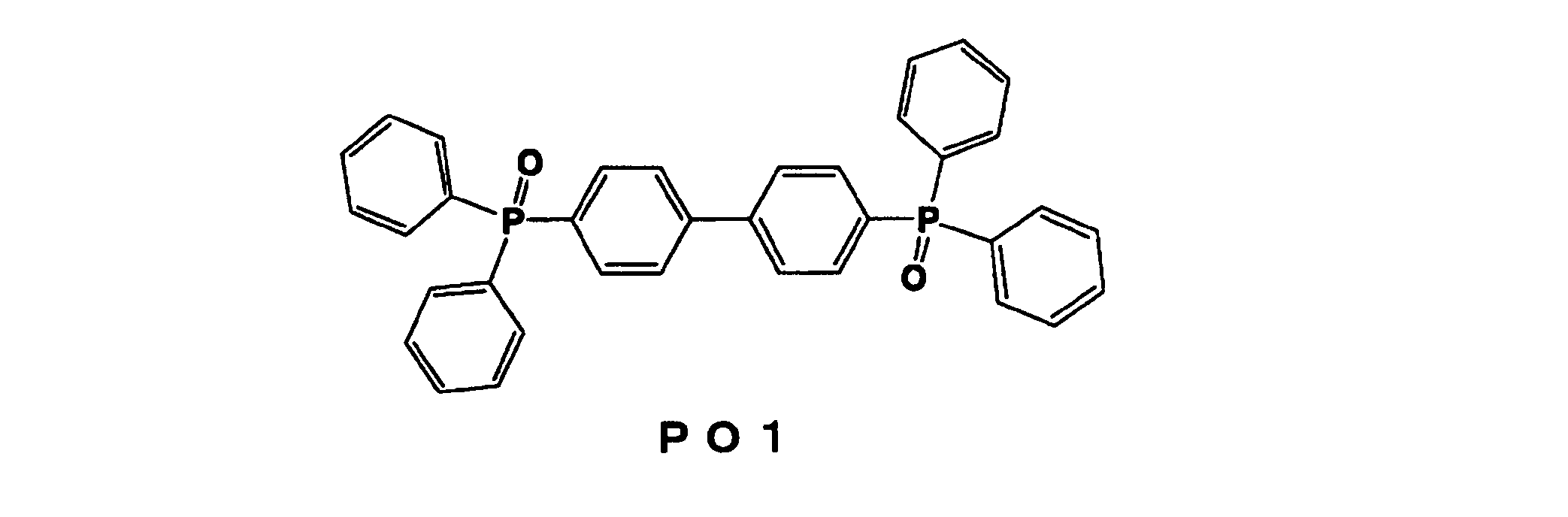
下記2,2’-ビス(4-カルバゾール-9-イル)フェニル)-ビフェニル(BCBP)は、発光層(ホスト材料)の材質として好適であり、両末端側のカルバゾール骨格と中央付近の四つのベンゼン骨格は同一平面上になく、互いに平行でないπ電子共役面を有する。そして、HOMOはカルバゾール骨格に主に分布している。したがって、カルバゾール骨格のπ電子共役面が基板表面に対して実質的に平行となるように、BCBPを配向させることで、正孔移動度を高くできると考えられる。一方、LUMOは、四つのベンゼン骨格に主に分布している。したがって、これらベンゼン骨格のπ電子共役面が基板表面に対して実質的に平行となるように、BCBPを配向させることで、電子移動度を高くできると考えられる。

下記2,8-ビス(ジフェニルフォスフォリル)ジベンゾ[b,d]チオフェン(PPT)は、発光層(ホスト材料)の材質として好適であり、中央付近のジベンゾチオフェン骨格とベンゼン骨格とが互いに平行でないπ電子共役面を有し、HOMO及びLUMOがジベンゾチオフェン骨格に主に分布している。したがって、ジベンゾチオフェン骨格のπ電子共役面が基板表面に対して実質的に平行となるように、PPTを配向させることで、キャリア移動度を高くできると考えられる。

下記4-(ジフェニルフォスフォイル)-N,N-ジフェニルアニリン(HM-A1)は、発光層(ホスト材料)の材質として好適であり、各ベンゼン骨格が別々に互いに平行でないπ電子共役面を有する。そして、HOMOはN,N-ジフェニルアニリン骨格に主に分布している。したがって、N,N-ジフェニルアニリン骨格のπ電子共役面が基板表面に対して実質的に平行となるように、HM-A1を配向させることで、正孔移動度を高くできると考えられる。一方、LUMOは、窒素原子及びリン原子で挟まれたベンゼン骨格に主に分布している。したがって、このベンゼン骨格のπ電子共役面が基板表面に対して実質的に平行となるように、HM-A1を配向させることで、電子移動度を高くできると考えられる。

下記9,9’-((2,6-ジフェニルベンゾ[1,2-b:4,5-b’]ジフラン-3,7-ジイル)ビス(4,1-フェニレン))ビス(9H-カルバゾール)(CZBDF)は、発光層(ホスト材料)の材質として好適であり、ベンゾジフラン骨格と両末端側のカルバゾール骨格、その他のベンゼン骨格が互いに平行でないπ電子共役面を有し、HOMO及びLUMOがベンゾジフラン骨格に主に分布している。したがって、ベンゾジフラン骨格のπ電子共役面が基板表面に対して実質的に平行となるように、CZBDFを配向させることで、キャリア移動度を高くできると考えられる。
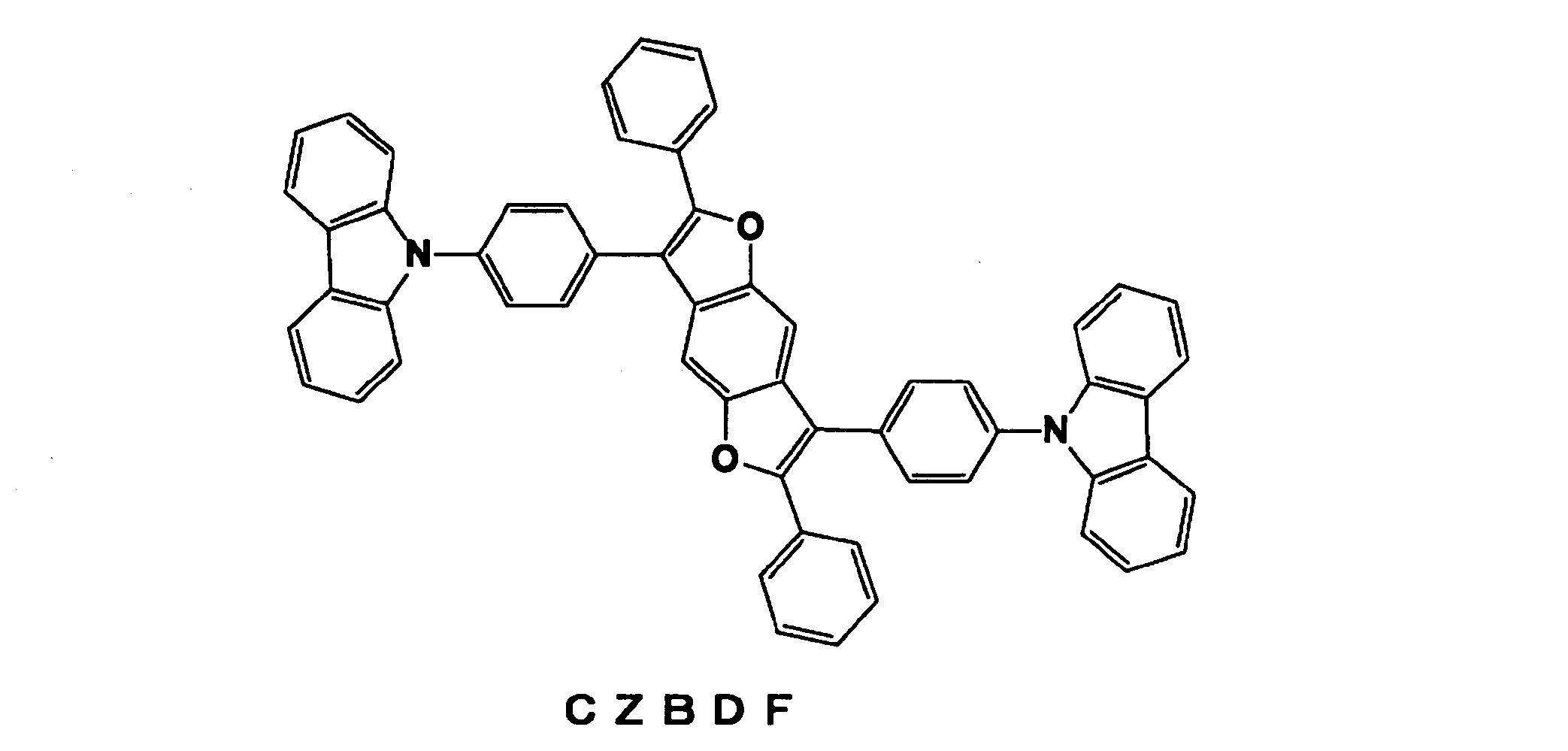
下記2,4-ビス(フェノキシ)-6-(3-メチルジフェニルアミノ)-1,3,5-トリアジン(BPMT)は、発光層(ホスト材料)の材質として好適であり、トリアジン骨格、各ベンゼン骨格が互いに平行でないπ電子共役面を有する。そして、HOMOはジフェニルアミノ骨格に主に分布している。したがって、ジフェニルアミノ骨格のπ電子共役面が基板表面に対して実質的に平行となるように、BPMTを配向させることで、正孔移動度を高くできると考えられる。一方、LUMOは、トリアジン骨格と、酸素原子に結合しているベンゼン骨格とに主に分布している。したがって、これらトリアジン骨格、ベンゼン骨格のπ電子共役面が基板表面に対して実質的に平行となるように、BPMTを配向させることで、電子移動度を高くできると考えられる。
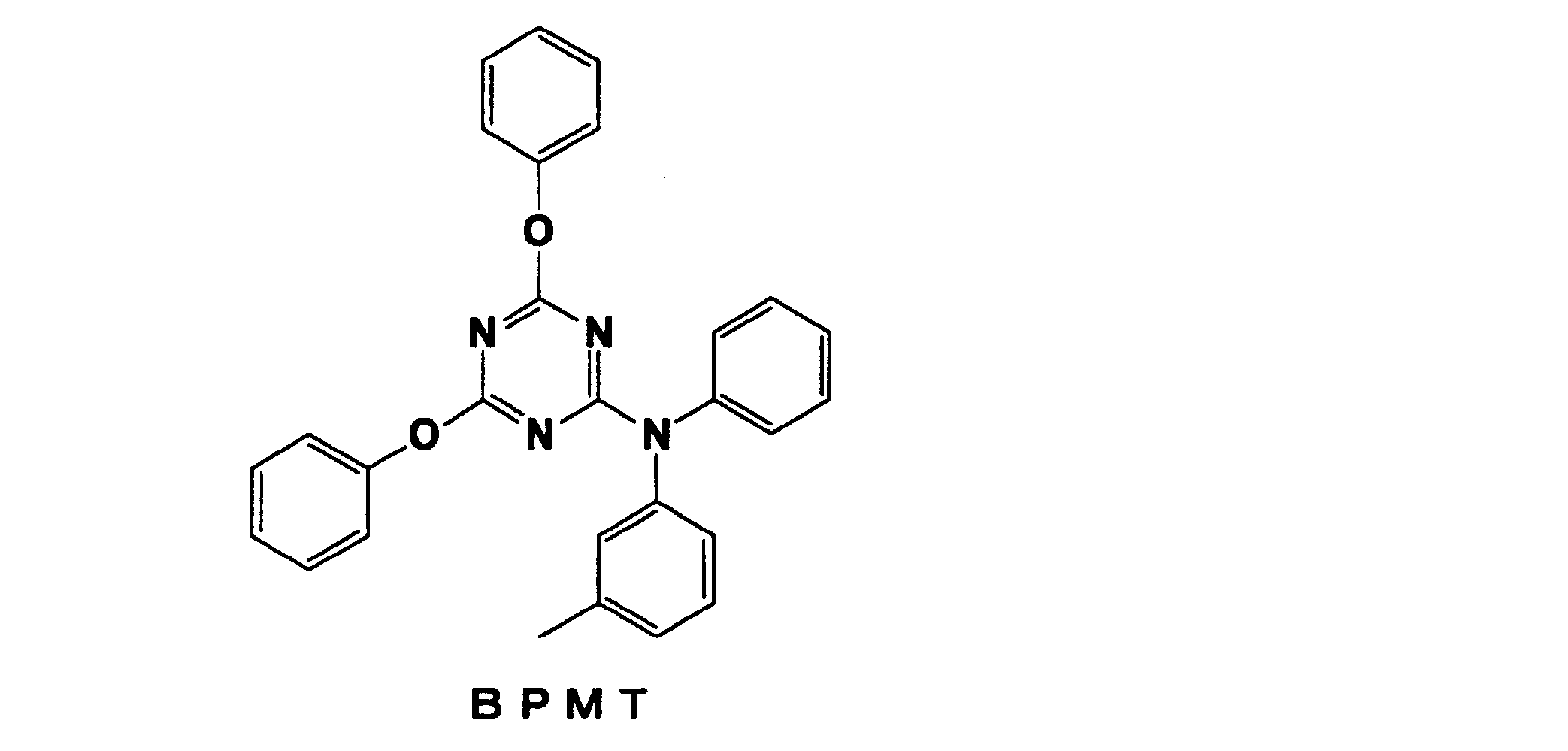
下記2,2’,2”-(1,3,5-ベンジントリル)-トリス(1-フェニル-1H-ベンゾイミダゾール)(TPBI)は、電子輸送層又は電子注入層の材質として好適であり、各ベンゾイミダゾール骨格と各ベンゼン骨格は互いに平行でないπ電子共役面を有し、電子輸送に関与するLUMOが中央付近のベンゼン骨格(三つのベンゾイミダゾール骨格が結合しているベンゼン骨格)に主に分布している。したがって、このベンゼン骨格のπ電子共役面が基板表面に対して実質的に平行となるように、TPBIを配向させることで、キャリア移動度を高くできると考えられる。

下記3-(4-ビフェニル)-4-フェニル-5-tert-ブチルフェニル-1,2,4-トリアゾール(TAZ)は、電子輸送層又は電子注入層の材質として好適であり、トリアゾール骨格と各ベンゼン骨格は互いに平行でないπ電子共役面を有し、電子輸送に関与するLUMOが、ビフェニル基を構成する二つのベンゼン骨格のうち、トリアゾール骨格に結合しているものに主に分布している。したがって、このベンゼン骨格のπ電子共役面が基板表面に対して実質的に平行となるように、TAZを配向させることで、キャリア移動度を高くできると考えられる。

下記4,7-ジフェニル-1,10-フェナントロリン(BPhen)は、電子輸送層又は電子注入層の材質として好適であり、フェナントロリン骨格と各ベンゼン骨格は互いに平行でないπ電子共役面を有し、電子輸送に関与するLUMOがフェナントロリン骨格に主に分布している。したがって、フェナントロリン骨格のπ電子共役面が基板表面に対して実質的に平行となるように、BPhenを配向させることで、キャリア移動度を高くできると考えられる。

下記ジフェニルビス(4-(ピリジン-3-イル)フェニル)シラン(DPPS)は、電子輸送層又は電子注入層の材質として好適であり、各ピリジン骨格と各ベンゼン骨格は互いに平行でないπ電子共役面を有し、電子輸送に関与するLUMOが、ピリジン骨格と、このピリジン骨格に結合しているベンゼン骨格に主に分布している。したがって、これらピリジン骨格、ベンゼン骨格のπ電子共役面が基板表面に対して実質的に平行となるように、DPPSを配向させることで、キャリア移動度を高くできると考えられる。

下記1,3,5-トリ[(3-ピリジル)-フェン-3-イル]ベンゼン(TmPyPB)は、電子輸送層又は電子注入層の材質として好適であり、各ピリジン骨格と各ベンゼン骨格は互いに平行でないπ電子共役面を有し、電子輸送に関与するLUMOが四つのベンゼン骨格に主に分布している。したがって、これらベンゼン骨格のπ電子共役面が基板表面に対して実質的に平行となるように、TmPyPBを配向させることで、キャリア移動度を高くできると考えられる。

下記1,3,5-トリ[(3-ピリジル)-フェン-3-イル]ベンゼン(TpPyPB)は、電子輸送層又は電子注入層の材質として好適であり、各ピリジン骨格と各ベンゼン骨格は互いに平行でないπ電子共役面を有し、電子輸送に関与するLUMOが四つのベンゼン骨格に主に分布している。したがって、これらベンゼン骨格のπ電子共役面が基板表面に対して実質的に平行となるように、TpPyPBを配向させることで、キャリア移動度を高くできると考えられる。

<表示装置>
前記有機EL素子を備えた表示装置としては、画像信号出力部と、駆動部と、発光部とを備えるものが例示できる。画像信号出力部は、画像信号を発生して出力する。駆動部は、前記画像信号に基づいて電流又は電圧を発生する。発光部は、前記有機EL素子であり、発生した前記電流又は電圧により発光する。そして、この有機EL素子を備えたこと以外は、従来の表示装置と同様の構成とすることができる。このような表示装置は、前記有機EL素子を備えたことで、電力消費量が少ないものとなる。
以下、図面を参照しながら説明する。
前記有機EL素子を備えた表示装置としては、画像信号出力部と、駆動部と、発光部とを備えるものが例示できる。画像信号出力部は、画像信号を発生して出力する。駆動部は、前記画像信号に基づいて電流又は電圧を発生する。発光部は、前記有機EL素子であり、発生した前記電流又は電圧により発光する。そして、この有機EL素子を備えたこと以外は、従来の表示装置と同様の構成とすることができる。このような表示装置は、前記有機EL素子を備えたことで、電力消費量が少ないものとなる。
以下、図面を参照しながら説明する。
図9A~図9Cは、前記有機EL素子を備えた表示装置の一実施形態の要部を例示する概略図である。図9Aは、図1に示す有機EL素子を備えた表示装置の一実施形態の要部を例示する平面図である。図9Bは、図1に示す有機EL素子を備えた表示装置の一実施形態の要部を例示する1画素の等価回路図である。図9Cは、図1に示す有機EL素子を備えた表示装置の一実施形態の要部を例示する1画素の平面図である。
ここに示す表示装置5Aは、前記有機EL素子1を用いた有機EL表示装置である。
表示装置5Aにおいては、複数の走査線(ゲート配線)50と、複数の信号線(ソース配線)51とが縦横に配されたマトリクスが形成されており、それぞれの交差部近傍に一つの画素が設けられた画素アレイが形成されている。画素アレイの周囲領域には、走査線50に接続された走査線駆動回路(ゲートドライバ)55と、信号線51に接続された信号線駆動回路(ソースドライバ)56が、それぞれ配置されている。そして、前記走査線駆動回路55及び信号線駆動回路56には、画像表示を行うためのタイミング信号やRGB輝度信号等の画像信号を供給するためのコントローラ57が接続され、さらに走査線50及び信号線51に与える信号電圧を供給するための電源回路59が接続されている。コントローラ57には、表示装置5Aに対して外部より水平・垂直同期信号や画像信号を与えるための外部処理装置58が接続されている。
表示装置5Aを構成する画素アレイの1画素は、図9Bに示すように、走査線50及び信号線51に接続されたスイッチング用トランジスタ52、画素を駆動するための駆動用トランジスタ53、並びに保持容量54を備え、駆動用トランジスタ53に有機EL素子1からなる画素部が接続されている。有機EL素子1は、駆動電流又は電圧により発光する。
スイッチング用トランジスタ52及び駆動用トランジスタ53は、例えば、一般的な多結晶シリコンを半導体として用いたトランジスタ等で構成できる。以上により表示装置5Aが構成されている。
有機EL素子としては、図1に示すものに限定されず、本実施形態に係る有機EL素子であれば、いずれも用いることができる。
ここに示す表示装置5Aは、前記有機EL素子1を用いた有機EL表示装置である。
表示装置5Aにおいては、複数の走査線(ゲート配線)50と、複数の信号線(ソース配線)51とが縦横に配されたマトリクスが形成されており、それぞれの交差部近傍に一つの画素が設けられた画素アレイが形成されている。画素アレイの周囲領域には、走査線50に接続された走査線駆動回路(ゲートドライバ)55と、信号線51に接続された信号線駆動回路(ソースドライバ)56が、それぞれ配置されている。そして、前記走査線駆動回路55及び信号線駆動回路56には、画像表示を行うためのタイミング信号やRGB輝度信号等の画像信号を供給するためのコントローラ57が接続され、さらに走査線50及び信号線51に与える信号電圧を供給するための電源回路59が接続されている。コントローラ57には、表示装置5Aに対して外部より水平・垂直同期信号や画像信号を与えるための外部処理装置58が接続されている。
表示装置5Aを構成する画素アレイの1画素は、図9Bに示すように、走査線50及び信号線51に接続されたスイッチング用トランジスタ52、画素を駆動するための駆動用トランジスタ53、並びに保持容量54を備え、駆動用トランジスタ53に有機EL素子1からなる画素部が接続されている。有機EL素子1は、駆動電流又は電圧により発光する。
スイッチング用トランジスタ52及び駆動用トランジスタ53は、例えば、一般的な多結晶シリコンを半導体として用いたトランジスタ等で構成できる。以上により表示装置5Aが構成されている。
有機EL素子としては、図1に示すものに限定されず、本実施形態に係る有機EL素子であれば、いずれも用いることができる。
以下、具体的実施例により、本発明の態様についてより詳細に説明する。ただし、本発明の態様は以下に示す実施例に何ら限定されるものではない。
<素子の製造>
[実施例1]
下記手順により、図10に示す構成を有する有機EL素子2を製造した。なお、図10では、図1に示す有機EL素子1の構成要素と同じものには、図1と同じ符号を付し、その詳細な説明は省略する。これは以降においても同様である。
厚さ0.7mmのガラス基板(基材11)上に、厚さ120nmのIZO膜(第一電極12、陽極)が成膜された基板を用い、これを水洗後、アルカリ性水溶液中で超音波洗浄を30分間行い、水洗後、超純水で超音波洗浄を15分間行って、110℃で30分間乾燥させた。
次いで、UVオゾンクリーナーを用いて、得られた基板を大気雰囲気下でUV-オゾン処理した。そして、基板を真空蒸着機にセットし、IZO膜上に酸化モリブデン(MoO3)膜(正孔注入層13a)を1nmの膜厚で成膜した後、4,4’,4”-トリス(カルバゾール-9-イル)トリフェニルアミン(TCTA、Tg151℃)膜(正孔注入層13a)を20nmの膜厚で成膜し、さらに、MADN(Tg120℃)膜(正孔輸送層13b)を20nmの膜厚で成膜した。この基板をグローブボックス内にセットし、窒素雰囲気下、135℃で30分間加熱処理した。
次いで、得られた基板を真空蒸着機にセットし、4,4’-ビス(カルバゾール-9-イル)ビフェニル(CBP、ホスト材料、Tg62℃)中に6質量%の濃度でトリス(2-フェニルピリジナート)イリジウム(Ir(ppy)3、ドーパント)をドープした膜(発光層13c)を、20nmの膜厚でMADN膜上に成膜し、TmPyPB(Tg79℃)膜(電子輸送層13e)を40nmの膜厚で成膜した。この基板をグローブボックス内にセットし、窒素雰囲気下、85℃で30分間加熱処理した。
次いで、得られた基板を真空蒸着機にセットし、シャドウマスクを基板のTmPyPB膜上に設置し、フッ化リチウム(LiF)膜(電子注入層13f)を1nmの膜厚で成膜し、アルミニウム(Al)膜(第二電極14、陰極)を100nmの膜厚で成膜することにより、陰極及び配線を形成した。そして、光硬化性樹脂を用いて、得られた基板をガラスで封止(図示略)することで、有機EL素子2を製造した。なお、図10において、符号23は有機EL層を示す。また、正孔注入層13aは、MoO3からなる層及びTCTAからなる層が積層された二層構造のものを一纏めに示している。
[実施例1]
下記手順により、図10に示す構成を有する有機EL素子2を製造した。なお、図10では、図1に示す有機EL素子1の構成要素と同じものには、図1と同じ符号を付し、その詳細な説明は省略する。これは以降においても同様である。
厚さ0.7mmのガラス基板(基材11)上に、厚さ120nmのIZO膜(第一電極12、陽極)が成膜された基板を用い、これを水洗後、アルカリ性水溶液中で超音波洗浄を30分間行い、水洗後、超純水で超音波洗浄を15分間行って、110℃で30分間乾燥させた。
次いで、UVオゾンクリーナーを用いて、得られた基板を大気雰囲気下でUV-オゾン処理した。そして、基板を真空蒸着機にセットし、IZO膜上に酸化モリブデン(MoO3)膜(正孔注入層13a)を1nmの膜厚で成膜した後、4,4’,4”-トリス(カルバゾール-9-イル)トリフェニルアミン(TCTA、Tg151℃)膜(正孔注入層13a)を20nmの膜厚で成膜し、さらに、MADN(Tg120℃)膜(正孔輸送層13b)を20nmの膜厚で成膜した。この基板をグローブボックス内にセットし、窒素雰囲気下、135℃で30分間加熱処理した。
次いで、得られた基板を真空蒸着機にセットし、4,4’-ビス(カルバゾール-9-イル)ビフェニル(CBP、ホスト材料、Tg62℃)中に6質量%の濃度でトリス(2-フェニルピリジナート)イリジウム(Ir(ppy)3、ドーパント)をドープした膜(発光層13c)を、20nmの膜厚でMADN膜上に成膜し、TmPyPB(Tg79℃)膜(電子輸送層13e)を40nmの膜厚で成膜した。この基板をグローブボックス内にセットし、窒素雰囲気下、85℃で30分間加熱処理した。
次いで、得られた基板を真空蒸着機にセットし、シャドウマスクを基板のTmPyPB膜上に設置し、フッ化リチウム(LiF)膜(電子注入層13f)を1nmの膜厚で成膜し、アルミニウム(Al)膜(第二電極14、陰極)を100nmの膜厚で成膜することにより、陰極及び配線を形成した。そして、光硬化性樹脂を用いて、得られた基板をガラスで封止(図示略)することで、有機EL素子2を製造した。なお、図10において、符号23は有機EL層を示す。また、正孔注入層13aは、MoO3からなる層及びTCTAからなる層が積層された二層構造のものを一纏めに示している。
[比較例1]
MADN膜の成膜後、及びTmPyPB膜の成膜後に、いずれも加熱処理しなかったこと以外は、実施例1と同様に、有機EL素子を製造した。
MADN膜の成膜後、及びTmPyPB膜の成膜後に、いずれも加熱処理しなかったこと以外は、実施例1と同様に、有機EL素子を製造した。
[実施例2]
下記手順により、図11に示す有機EL素子3を製造した。
厚さ0.7mmのガラス基板(基材11)上に、厚さ120nmのIZO膜(第一電極12、陽極)が成膜された基板を用い、これを水洗後、アルカリ性水溶液中で超音波洗浄を30分間行い、水洗後、超純水で超音波洗浄を15分間行って、110℃で30分間乾燥させた。
次いで、UVオゾンクリーナーを用いて、得られた基板を大気雰囲気下でUV-オゾン処理した。そして、基板を真空蒸着機にセットし、IZO膜上に2-メチル-9,10-ビス(ナフタレン-2-イル)アントラセン(MADN、Tg120℃)膜(正孔輸送層13b)を50nmの膜厚で成膜した。そして、この基板をグローブボックス内にセットし、窒素雰囲気下、135℃で30分間加熱処理した。
次いで、得られた基板を真空蒸着機にセットし、MADN膜上に1,3,5-トリ[(3-ピリジル)-フェン-3-イル]ベンゼン(TmPyPB、Tg79℃)膜(電子輸送層13e)を50nmの膜厚で成膜した。そして、この基板をグローブボックス内にセットし、窒素雰囲気下、85℃で30分間加熱処理した。
次いで、得られた基板を真空蒸着機にセットし、シャドウマスクを基板のTmPyPB膜上に設置し、フッ化リチウム(LiF)膜(電子注入層13f)を1nmの膜厚で成膜し、アルミニウム(Al)膜(第二電極14、陰極)を100nmの膜厚で成膜することにより、陰極及び配線を形成した。そして、光硬化性樹脂を用いて、得られた基板をガラスで封止(図示略)することで、有機EL素子3を製造した。なお、図11において、符号33は有機EL層を示す。
下記手順により、図11に示す有機EL素子3を製造した。
厚さ0.7mmのガラス基板(基材11)上に、厚さ120nmのIZO膜(第一電極12、陽極)が成膜された基板を用い、これを水洗後、アルカリ性水溶液中で超音波洗浄を30分間行い、水洗後、超純水で超音波洗浄を15分間行って、110℃で30分間乾燥させた。
次いで、UVオゾンクリーナーを用いて、得られた基板を大気雰囲気下でUV-オゾン処理した。そして、基板を真空蒸着機にセットし、IZO膜上に2-メチル-9,10-ビス(ナフタレン-2-イル)アントラセン(MADN、Tg120℃)膜(正孔輸送層13b)を50nmの膜厚で成膜した。そして、この基板をグローブボックス内にセットし、窒素雰囲気下、135℃で30分間加熱処理した。
次いで、得られた基板を真空蒸着機にセットし、MADN膜上に1,3,5-トリ[(3-ピリジル)-フェン-3-イル]ベンゼン(TmPyPB、Tg79℃)膜(電子輸送層13e)を50nmの膜厚で成膜した。そして、この基板をグローブボックス内にセットし、窒素雰囲気下、85℃で30分間加熱処理した。
次いで、得られた基板を真空蒸着機にセットし、シャドウマスクを基板のTmPyPB膜上に設置し、フッ化リチウム(LiF)膜(電子注入層13f)を1nmの膜厚で成膜し、アルミニウム(Al)膜(第二電極14、陰極)を100nmの膜厚で成膜することにより、陰極及び配線を形成した。そして、光硬化性樹脂を用いて、得られた基板をガラスで封止(図示略)することで、有機EL素子3を製造した。なお、図11において、符号33は有機EL層を示す。
[比較例2]
MADN膜の成膜後、及びTmPyPB膜の成膜後に、いずれも加熱処理しなかったこと以外は、実施例2と同様に、有機EL素子を製造した。
MADN膜の成膜後、及びTmPyPB膜の成膜後に、いずれも加熱処理しなかったこと以外は、実施例2と同様に、有機EL素子を製造した。
<薄膜の電気的特性の評価>
上記実施例及び比較例で得られた素子の電流-電圧(I-V)特性を測定し、有機薄膜の電気的特性を評価した。実施例2及び比較例2の電流-電圧特性の測定結果を図12に示す。
その結果、実施例1の方が比較例1よりも、印加電圧に対して電流が流れ易く、電圧4Vにおける電流密度は、実施例1が比較例1よりも10倍高かった。
また、実施例2の方が比較例2よりも、印加電圧に対して電流が流れ易く、電圧1Vにおける電流密度は、実施例2が比較例2よりも200倍高かった。
上記実施例及び比較例で得られた素子の電流-電圧(I-V)特性を測定し、有機薄膜の電気的特性を評価した。実施例2及び比較例2の電流-電圧特性の測定結果を図12に示す。
その結果、実施例1の方が比較例1よりも、印加電圧に対して電流が流れ易く、電圧4Vにおける電流密度は、実施例1が比較例1よりも10倍高かった。
また、実施例2の方が比較例2よりも、印加電圧に対して電流が流れ易く、電圧1Vにおける電流密度は、実施例2が比較例2よりも200倍高かった。
本発明の態様は、有機EL素子を備えた有機デバイスに利用可能である。
1,2,3・・・有機EL素子、11・・・基材、12・・・第一電極、13,23,33・・・有機EL層、13a・・・正孔注入層、13b・・・正孔輸送層、13c・・・発光層、13d・・・正孔ブロッキング層、13e・・・電子輸送層、13f・・・電子注入層、14・・・第二電極
Claims (8)
- 基材と、
前記基材上に設けられた一対の電極と、
前記一対の電極間に設けられた少なくとも二層の有機薄膜を有する有機エレクトロルミネッセンス層と、を備え
少なくとも二層の前記有機薄膜のうち、二層又はそれ以上の前記有機薄膜は、二層又はそれ以上の前記有機薄膜に含まれる材料のガラス転移点、又はガラス転移点を有していない場合には融点が高いほど、前記基材に近くなるように配置されている有機エレクトロルミネッセンス素子。 - 二層又はそれ以上の前記有機薄膜は発光層を含み、
前記発光層が、ホスト材料及び発光材料を含み、
二層又はそれ以上の前記有機薄膜は、前記発光材料以外の二層又はそれ以上の前記有機薄膜に含まれる材料のガラス転移点、又はガラス転移点を有していない場合には融点が高い層ほど、前記基材に近くなるように配置されている請求項1に記載の有機エレクトロルミネッセンス素子。 - 前記有機エレクトロルミネッセンス層が、二層又はそれ以上の前記有機薄膜として、発光層と、電子輸送層とを含み、
前記電子輸送層と前記基材との間に前記発光層が配置され、
前記発光層が、ホスト材料及び発光材料を含み、
前記ホスト材料のガラス転移点、又はガラス転移点を有していない場合には融点は、前記電子輸送層を構成する材料の前記ガラス転移点又は融点よりも高い請求項1に記載の有機エレクトロルミネッセンス素子。 - 前記有機エレクトロルミネッセンス層が、二層又はそれ以上の前記有機薄膜として、発光層と、正孔輸送層とを含み、
前記正孔輸送層と前記基材との間に前記発光層が配置され、
前記発光層が、ホスト材料及び発光材料を含み、
前記ホスト材料のガラス転移点、又はガラス転移点を有していない場合には融点は、前記正孔輸送層を構成する材料の前記ガラス転移点又は融点よりも高い請求項1に記載の有機エレクトロルミネッセンス素子。 - 二層又はそれ以上の前記有機薄膜は、互いに隣接し、
互いに隣接する二層又はそれ以上の前記有機薄膜は、前記有機薄膜を構成する材料の前記ガラス転移点又は融点の差が、10℃以上である請求項1に記載の有機エレクトロルミネッセンス素子。 - 前記有機薄膜の少なくとも一つに含まれる材料が、π電子共役有機分子である請求項1に記載の有機エレクトロルミネッセンス素子。
- 基材上に一方の電極、有機エレクトロルミネッセンス層、及び他方の電極をこの順に積層することを含み、
前記有機エレクトロルミネッセンス層の形成は、少なくとも二層の有機薄膜を形成することを含み、
少なくとも二層の前記有機薄膜のうち最下層以外は、その成膜中又は成膜後に、前記有機薄膜を構成する材料の前記ガラス転移点又は融点よりも20℃低い温度から20℃高い温度の温度域で、且つ直前に成膜した有機薄膜を構成する材料の前記ガラス転移点又は融点よりも低い温度で加熱処理されることを含む有機エレクトロルミネッセンス素子の製造方法。 - 前記有機エレクトロルミネッセンス層の形成は、少なくとも二層の前記有機薄膜のうち最下層以外が、その成膜中又は成膜後に、前記有機薄膜を構成する材料の前記ガラス転移点又は融点よりも20℃低い温度から20℃高い温度の温度域で、且つ直前に成膜した有機薄膜を構成する材料の前記ガラス転移点又は融点よりも10℃以上低い温度で加熱処理される請求項7に記載の有機エレクトロルミネッセンス素子の製造方法。
Applications Claiming Priority (2)
| Application Number | Priority Date | Filing Date | Title |
|---|---|---|---|
| JP2011168595A JP2014199830A (ja) | 2011-08-01 | 2011-08-01 | 有機エレクトロルミネッセンス素子及びその製造方法 |
| JP2011-168595 | 2011-08-01 |
Publications (1)
| Publication Number | Publication Date |
|---|---|
| WO2013018661A1 true WO2013018661A1 (ja) | 2013-02-07 |
Family
ID=47629186
Family Applications (1)
| Application Number | Title | Priority Date | Filing Date |
|---|---|---|---|
| PCT/JP2012/069034 Ceased WO2013018661A1 (ja) | 2011-08-01 | 2012-07-26 | 有機エレクトロルミネッセンス素子及びその製造方法 |
Country Status (2)
| Country | Link |
|---|---|
| JP (1) | JP2014199830A (ja) |
| WO (1) | WO2013018661A1 (ja) |
Cited By (2)
| Publication number | Priority date | Publication date | Assignee | Title |
|---|---|---|---|---|
| WO2015105315A1 (ko) * | 2014-01-10 | 2015-07-16 | 삼성에스디아이 주식회사 | 축합환 화합물, 및 이를 포함한 유기 발광 소자 |
| EP3054745A4 (en) * | 2013-10-01 | 2017-06-28 | Sumitomo Chemical Company Limited | Light emitting element |
Citations (6)
| Publication number | Priority date | Publication date | Assignee | Title |
|---|---|---|---|---|
| JP2000077192A (ja) * | 1998-09-01 | 2000-03-14 | Pioneer Electronic Corp | 有機エレクトロルミネッセンスパネルとその製造方法 |
| JP2005005149A (ja) * | 2003-06-12 | 2005-01-06 | Tohoku Pioneer Corp | 有機el素子及びその製造方法 |
| WO2006117914A1 (ja) * | 2005-04-27 | 2006-11-09 | Konica Minolta Holdings, Inc. | 有機エレクトロルミネッセンス素子の製造方法 |
| JP2007311223A (ja) * | 2006-05-19 | 2007-11-29 | Konica Minolta Holdings Inc | 有機el素子の製造方法 |
| JP2008034280A (ja) * | 2006-07-31 | 2008-02-14 | Sony Corp | 表示装置の製造方法 |
| JP2009283491A (ja) * | 2008-05-19 | 2009-12-03 | Toyota Central R&D Labs Inc | 有機発光素子およびその製造方法 |
-
2011
- 2011-08-01 JP JP2011168595A patent/JP2014199830A/ja not_active Withdrawn
-
2012
- 2012-07-26 WO PCT/JP2012/069034 patent/WO2013018661A1/ja not_active Ceased
Patent Citations (6)
| Publication number | Priority date | Publication date | Assignee | Title |
|---|---|---|---|---|
| JP2000077192A (ja) * | 1998-09-01 | 2000-03-14 | Pioneer Electronic Corp | 有機エレクトロルミネッセンスパネルとその製造方法 |
| JP2005005149A (ja) * | 2003-06-12 | 2005-01-06 | Tohoku Pioneer Corp | 有機el素子及びその製造方法 |
| WO2006117914A1 (ja) * | 2005-04-27 | 2006-11-09 | Konica Minolta Holdings, Inc. | 有機エレクトロルミネッセンス素子の製造方法 |
| JP2007311223A (ja) * | 2006-05-19 | 2007-11-29 | Konica Minolta Holdings Inc | 有機el素子の製造方法 |
| JP2008034280A (ja) * | 2006-07-31 | 2008-02-14 | Sony Corp | 表示装置の製造方法 |
| JP2009283491A (ja) * | 2008-05-19 | 2009-12-03 | Toyota Central R&D Labs Inc | 有機発光素子およびその製造方法 |
Cited By (8)
| Publication number | Priority date | Publication date | Assignee | Title |
|---|---|---|---|---|
| EP3054745A4 (en) * | 2013-10-01 | 2017-06-28 | Sumitomo Chemical Company Limited | Light emitting element |
| WO2015105315A1 (ko) * | 2014-01-10 | 2015-07-16 | 삼성에스디아이 주식회사 | 축합환 화합물, 및 이를 포함한 유기 발광 소자 |
| WO2015105313A1 (ko) * | 2014-01-10 | 2015-07-16 | 삼성에스디아이 주식회사 | 축합환 화합물, 및 이를 포함한 유기 발광 소자 |
| WO2015105316A1 (ko) * | 2014-01-10 | 2015-07-16 | 삼성에스디아이 주식회사 | 축합환 화합물, 및 이를 포함한 유기 발광 소자 |
| CN105899518A (zh) * | 2014-01-10 | 2016-08-24 | 三星Sdi株式会社 | 稠环化合物以及含有其的有机发光元件 |
| CN105899517A (zh) * | 2014-01-10 | 2016-08-24 | 三星Sdi株式会社 | 稠环化合物以及含有其的有机发光装置 |
| CN105934436A (zh) * | 2014-01-10 | 2016-09-07 | 三星Sdi株式会社 | 稠环化合物以及含有其的有机发光元件 |
| CN105899517B (zh) * | 2014-01-10 | 2019-05-21 | 三星Sdi株式会社 | 稠环化合物以及含有其的有机发光装置 |
Also Published As
| Publication number | Publication date |
|---|---|
| JP2014199830A (ja) | 2014-10-23 |
Similar Documents
| Publication | Publication Date | Title |
|---|---|---|
| CN104137289B (zh) | 发光元件 | |
| TWI586014B (zh) | 包含多層電洞傳輸層之有機發光二極體及包含該有機發光二極體之平面顯示裝置 | |
| TWI592464B (zh) | 有機電場發光元件 | |
| CN105849930B (zh) | 有机发光元件 | |
| KR101753428B1 (ko) | 발광 소자, 발광 장치, 조명 장치 및 전자 기기 | |
| US11114620B2 (en) | Organic light-emitting diode device and compound for charge generation layer included therein | |
| JP5397568B1 (ja) | 発光素子材料および発光素子 | |
| CN103430344B (zh) | 发光元件材料及发光元件 | |
| US12369490B2 (en) | Organic electroluminescent element, organic electroluminescent display device, and electronic device | |
| CN102918677A (zh) | 发光元件 | |
| KR20170029708A (ko) | 유기 발광 소자 | |
| CN103250264A (zh) | 发光元件材料及发光元件 | |
| Lim et al. | Enhanced triplet–triplet annihilation of blue fluorescent organic light-emitting diodes by generating excitons in trapped charge-free regions | |
| US20250351666A1 (en) | Organic el display device, and electronic apparatus | |
| JP2025016806A (ja) | 有機エレクトロルミネッセンス素子及び電子機器 | |
| WO2024090353A1 (ja) | 化合物、発光素子材料、発光素子、表示装置および照明装置 | |
| JP2013030406A (ja) | キャリア輸送性有機非晶質薄膜の製造方法 | |
| KR20230126721A (ko) | 유기 일렉트로루미네센스 소자, 발광 장치, 유기 일렉트로루미네센스표시 장치 및 전자 기기 | |
| JP6490685B2 (ja) | 電気光学素子およびその使用 | |
| JP4802671B2 (ja) | 低分子有機薄膜を備える有機el素子 | |
| WO2013018661A1 (ja) | 有機エレクトロルミネッセンス素子及びその製造方法 | |
| JP2016525781A (ja) | 電気光学素子およびその使用 | |
| CN103996795A (zh) | 有机发光元件 | |
| KR20230125260A (ko) | 유기 일렉트로루미네센스 소자 및 전자 기기 | |
| JP2013030674A (ja) | 電荷輸送性有機薄膜および有機エレクトロルミネッセンス素子 |
Legal Events
| Date | Code | Title | Description |
|---|---|---|---|
| 121 | Ep: the epo has been informed by wipo that ep was designated in this application |
Ref document number: 12820432 Country of ref document: EP Kind code of ref document: A1 |
|
| NENP | Non-entry into the national phase |
Ref country code: DE |
|
| 122 | Ep: pct application non-entry in european phase |
Ref document number: 12820432 Country of ref document: EP Kind code of ref document: A1 |
|
| NENP | Non-entry into the national phase |
Ref country code: JP |