WO2013021815A1 - Dispositif d'analyse à base de nanopore - Google Patents
Dispositif d'analyse à base de nanopore Download PDFInfo
- Publication number
- WO2013021815A1 WO2013021815A1 PCT/JP2012/068765 JP2012068765W WO2013021815A1 WO 2013021815 A1 WO2013021815 A1 WO 2013021815A1 JP 2012068765 W JP2012068765 W JP 2012068765W WO 2013021815 A1 WO2013021815 A1 WO 2013021815A1
- Authority
- WO
- WIPO (PCT)
- Prior art keywords
- electrode
- nanopore
- sample
- biopolymer
- electrodes
- Prior art date
- Legal status (The legal status is an assumption and is not a legal conclusion. Google has not performed a legal analysis and makes no representation as to the accuracy of the status listed.)
- Ceased
Links
Images











Classifications
-
- G—PHYSICS
- G01—MEASURING; TESTING
- G01N—INVESTIGATING OR ANALYSING MATERIALS BY DETERMINING THEIR CHEMICAL OR PHYSICAL PROPERTIES
- G01N27/00—Investigating or analysing materials by the use of electric, electrochemical, or magnetic means
- G01N27/26—Investigating or analysing materials by the use of electric, electrochemical, or magnetic means by investigating electrochemical variables; by using electrolysis or electrophoresis
- G01N27/416—Systems
- G01N27/447—Systems using electrophoresis
- G01N27/44756—Apparatus specially adapted therefor
- G01N27/44791—Microapparatus
-
- G—PHYSICS
- G01—MEASURING; TESTING
- G01N—INVESTIGATING OR ANALYSING MATERIALS BY DETERMINING THEIR CHEMICAL OR PHYSICAL PROPERTIES
- G01N33/00—Investigating or analysing materials by specific methods not covered by groups G01N1/00 - G01N31/00
- G01N33/48—Biological material, e.g. blood, urine; Haemocytometers
- G01N33/483—Physical analysis of biological material
- G01N33/487—Physical analysis of biological material of liquid biological material
- G01N33/48707—Physical analysis of biological material of liquid biological material by electrical means
- G01N33/48721—Investigating individual macromolecules, e.g. by translocation through nanopores
-
- G—PHYSICS
- G01—MEASURING; TESTING
- G01N—INVESTIGATING OR ANALYSING MATERIALS BY DETERMINING THEIR CHEMICAL OR PHYSICAL PROPERTIES
- G01N33/00—Investigating or analysing materials by specific methods not covered by groups G01N1/00 - G01N31/00
- G01N33/48—Biological material, e.g. blood, urine; Haemocytometers
- G01N33/483—Physical analysis of biological material
- G01N33/487—Physical analysis of biological material of liquid biological material
- G01N33/48707—Physical analysis of biological material of liquid biological material by electrical means
- G01N33/48728—Investigating individual cells, e.g. by patch clamp, voltage clamp
Definitions
- the present invention relates to an apparatus for analyzing a biopolymer such as DNA or protein through nanometer-sized pores (referred to as nanopores in the present application).
- the present invention relates to a nanopore type analyzer that can improve the passing frequency of nanopores of biopolymers.
- Non-patent Document 1 Development of a method for analyzing high molecular polymers such as DNA and proteins using nanopores called nanopores is in progress. Although it was technically difficult to open the nanopore, it was first realized in the bio field by introducing an ion channel into a lipid bilayer (Non-patent Document 1). As a measurement method using nanopores, a method according to the patch clamp method used for biological ion channel measurement has been developed. Next, attempts have been made to open nanopores using a semiconductor process, and a method using an ion beam (Non-Patent Document 2) and a method using an electron beam (Non-Patent Document 3) have been developed.
- Non-Patent Document 2 a method using an ion beam
- Non-Patent Document 3 a method using an electron beam
- nanopores could be created, methods for analyzing macromolecules such as DNA and proteins using nanopores were developed.
- the main technologies required for nanopore analysis are the following two.
- Detection technology Detects physical changes as the polymer passes through the nanopore. Movement control technology: Moves a polymer and passes it through a nanopore As the detection technology, a blocking current method, a tunnel current method, and a capacitance method are known. The blocking current method is a method for detecting the influence of the polymer partially blocking the opening of the nanopore (Non-patent Document 4). As a specific structure, the space is separated into two by a film having nanopores, each space is filled with a liquid containing ions, and electrodes are arranged. When a constant voltage is applied to the electrode, ions move through the nanopore and current flows (ion passing current).
- the blocking current method is a method for analyzing the presence and components of a polymer by detecting this decrease in current value. In addition to the opening area, the difficulty of ion flow is affected by the charge state of the polymer and the interaction with the nanopore wall surface.
- Non-Patent Document 5 when the polymer passes through the nanopore, the tunnel current flows through a slight gap between the tunnel current electrode and the polymer provided in the vicinity of the nanopore, and this is detected. This is a method for analyzing the presence and components of the odorant (Non-Patent Document 5, Non-Patent Document 6).
- Capacitance method means that when the polymer passes through the nanopore, the nanopore is partially blocked, so the capacitor of the membrane having the nanopore changes, and the presence and components of the polymer are analyzed by detecting it. It is a method (nonpatent literature 7).
- the movement control technology includes a potential difference transfer method, an enzyme transfer method, and a mechanical transfer method.
- the potential difference transfer method is a method in which an electrode is placed in two spaces separated by a membrane having a nanopore and a voltage is applied to the electrode to generate an electric field. As an advantage, it can be realized with a simple structure, and no extra addition is applied to the polymer.
- the enzyme transfer method is a method in which an enzyme is placed in the vicinity of the nanopore and the polymer is moved using a reaction between the polymer and the enzyme.
- an enzyme is placed in the vicinity of the nanopore and the polymer is moved using a reaction between the polymer and the enzyme.
- the polymer is single-stranded DNA
- the mechanical movement method is a method for realizing the movement of the polymer by fixing the polymer to the beads and moving the beads with optical tweezers. In this method, it is necessary to put an end portion without a polymer bead into the nanopore, and at that time, a potential difference transfer method is adopted.
- the potential difference transfer method is used in combination with any method as a driving force for transporting the sample to the nanopore opening.
- the sample passes through the nanopore after passing through the following three movement states to the nanopore opening.
- the first is movement due to sample diffusion
- the second is movement due to electrophoresis
- the third is the probability that the tip reaches the nanopore opening when the sample is long chain (Non-patent Document 8).
- the influence of the potential difference is greatly involved.
- the present invention relates to a nanopore-type biopolymer analyzer capable of improving the throughput of a low-concentration sample through a nanopore and improving the throughput in a measurement method using nanopores, and a biopolymer using the same
- An object is to provide an analysis method.
- the inventors of the present invention applied a voltage to an electrode disposed in the vicinity of the nanopore, thereby expanding the potential difference in the vicinity of the nanopore opening on the side where the sample was introduced.
- the biopolymer contained therein was collected in the opening of the nanopore and passed through the nanopore efficiently, and the present invention was completed.
- the present invention includes the following.
- a nanopore biopolymer analyzer A chamber having a sample introduction section and a sample outflow section separated by a substrate; A first electrode provided in the sample introduction section and a second electrode provided in the sample outflow section; A thin film formed on the substrate; A nanopore provided in the thin film of the substrate and communicating the sample introduction section and the sample outflow section; A third electrode disposed in the vicinity of the nanopore of the substrate; Voltage applying means; Having a chamber with The voltage applying means includes means for applying a voltage between the first electrode and the third electrode, between the first electrode and the second electrode, and between the third electrode and the second electrode.
- a nanopore type biopolymer analyzer characterized by the above.
- a third electrode and the measurement electrode are arranged in parallel along the axial direction of the nanopore, and the measurement electrode is provided at a position closer to the sample outflow section than the third electrode.
- Nanopore type biopolymer analyzer is arranged in parallel along the axial direction of the nanopore, and the measurement electrode is provided at a position closer to the sample outflow section than the third electrode.
- a sample solution containing a biopolymer is introduced into the sample introduction section of the nanopore biopolymer analyzer of [1] to [14], and a voltage is applied between the third electrode and the first electrode.
- a method for analyzing a biopolymer comprising collecting a charged biopolymer by applying, passing the nanopore, and measuring the biopolymer passing through the nanopore.
- the first, second, and third electrodes so that the potential of the third electrode is lower than the potential of the first electrode and equal to or lower than the potential of the second electrode.
- a positively charged biopolymer is collected by changing the voltage so that the potential of the third electrode is higher than the potential of the second electrode, and then promotes passage through the nanopore.
- biopolymer is selected from the group consisting of nucleic acids, peptide nucleic acids, proteins, polypeptides, and sugar chains.
- the frequency with which biopolymers pass through nanopores can be increased, and the throughput in the nanopore measurement method can be improved.
- FIG. 1 It is a schematic diagram of the analysis chamber part of the nanopore type
- FIG. 3 is a schematic diagram of a nanopore substrate in which electrodes are arranged around the nanopore by retreating from the end of the nanopore. It is a schematic diagram of the nanopore substrate in which electrodes are arranged on the entire surface around the nanopore excluding a portion retracted from the end portion of the nanopore.
- FIG. 4 is a schematic view of a nanopore substrate in which electrodes are arranged in multiple locations by retreating from the end of the nanopore around the nanopore.
- FIG. 3 is a schematic view of a nanopore substrate in which electrodes are arranged in multiple and multiple layers by retreating from the end of the nanopore around the nanopore.
- FIG. 1 It is a schematic diagram of the chamber part for analysis provided with the nanopore board
- FIG. 1 It is a schematic diagram of an analysis chamber part provided with a nanopore substrate in which biological nanopores are directly arranged in holes of a solid film (thin film) and a sample collection electrode is provided in the vicinity of the nanopores.
- FIG. 1 It is a schematic diagram of the analysis chamber part in which a plurality of nanopores having sample collection electrodes are arranged.
- the present invention is characterized in that a biopolymer is collected in the vicinity of the nanopore by applying a voltage to an electrode arranged in the vicinity of the nanopore and increasing a potential difference in the vicinity of the nanopore, and the biopolymer is passed through the nanopore at a high frequency.
- the present invention relates to a nanopore type biopolymer analyzer and a biopolymer analysis method using the same.
- the nanopore type biopolymer analyzer has a chamber part and a substrate disposed therein.
- the substrate includes a base (base material), a thin film formed facing the base material, a nanopore provided in the thin film and communicating with the sample introduction section and the sample outflow section, and a sample disposed in the vicinity of the nanopore.
- the electrode has a collecting electrode (also referred to as a third electrode in the present specification) and the like, and is disposed between the sample introduction section and the sample outflow section of the chamber.
- the substrate may have an insulating layer disposed facing the sample collection electrode (third electrode).
- the substrate is preferably a solid substrate.
- the substrate can be formed of an electrically insulating material, such as an inorganic material and an organic material (including a polymer material), excluding the electrodes.
- the electrical insulator material constituting the substrate include silicon (silicon), silicon compound, glass, quartz, polydimethylsiloxane (PDMS), polytetrafluoroethylene (PTFE), polystyrene, and polypropylene.
- the silicon compound include silicon oxynitride such as silicon nitride, silicon oxide, and silicon carbide.
- the base (base material) constituting the support portion of the substrate can be made from any of these materials, but may be, for example, silicon or a silicon compound.
- the size and thickness of the substrate are not particularly limited as long as nanopores can be provided.
- substrate can be produced by a well-known method in this technical field, or can also be obtained as a commercial item.
- the substrate can be fabricated using photolithography or electron beam lithography and techniques such as etching, laser ablation, injection molding, casting, molecular beam epitaxy, chemical vapor deposition (CVD), electron beam or focused ion beam. .
- the substrate may be coated to avoid adsorption of other molecules to the surface.
- the thickness of the substrate is preferably 100 ⁇ m to 1000 ⁇ m.
- the substrate has at least one nanopore.
- the nanopore is provided in the thin film, but may be provided in the base (base material), the electrode, and the insulator simultaneously.
- nanopore and pore are pores of nanometer (nm) size (ie, a diameter of 1 nm or more and less than 1 ⁇ m), and communicate with the sample introduction section and the sample outflow section through the substrate. It is a hole.
- the substrate preferably has a thin film for providing nanopores. That is, by forming a thin film having a material and thickness suitable for forming nano-sized pores on the substrate, the nanopore can be easily and efficiently provided on the substrate.
- the material of the thin film is preferably silicon oxide (SiO 2 ), silicon nitride (SiN), silicon oxynitride (SiON), metal oxide, metal silicate, or the like.
- the thin film (and possibly the entire substrate) may be substantially transparent.
- substantially transparent means that external light can be transmitted through approximately 50% or more, preferably 80% or more.
- the thin film may be a single layer or a multilayer.
- the thickness of the thin film is 1 nm to 200 nm, preferably 1 nm to 50 nm, more preferably 1 nm to 20 nm.
- the thin film can be formed on the substrate by techniques known in the art, for example, by low pressure chemical vapor deposition (LPCVD).
- LPCVD low pressure chemical vapor deposition
- the thickness of the insulating layer is preferably 5 nm to 50 nm.
- any insulating material can be used for the insulating layer, for example, silicon or a silicon compound (silicon nitride, silicon oxide, etc.) is preferably used.
- the “opening” of the nanopore or the pore refers to the opening circle of the nanopore or the pore where the nanopore or the pore is in contact with the sample solution.
- biopolymers and ions in the sample solution enter the nanopore from one opening and exit the nanopore from the same or opposite opening.
- the size of the nanopore can be selected appropriately depending on the type of biopolymer to be analyzed.
- the nanopore may have a uniform diameter, but may have a different diameter depending on the site.
- the nanopore may be connected to a pore having a diameter of 1 ⁇ m or more.
- the nanopore provided on the thin film of the substrate has a minimum diameter portion, that is, the smallest diameter of the nanopore is 100 nm or less, for example, 1 nm to 100 nm, preferably 1 nm to 50 nm, for example 1 nm to 10 nm, specifically 1 nm or more. It is preferably 5 nm or less, 3 nm or more and 5 nm or less.
- a detection part by disposing a measurement electrode on the nanopore having a diameter of 100 nm or less, preferably 10 nm or less, for example, 1 nm to 100 nm or 1 nm to 5 nm.
- the diameter of ssDNA is about 1.5 nm, and an appropriate range of the nanopore diameter for analyzing ssDNA is about 1.5 to 10 nm, preferably about 1.5 to 2.5 nm.
- the diameter of dsDNA double-stranded DNA
- an appropriate range of nanopore diameter for analyzing dsDNA is about 3 nm to 10 nm, preferably about 3 nm to 5 nm.
- the nanopore diameter corresponding to the outer diameter of the biopolymer can be selected.
- the depth (length) of the nanopore can be adjusted by adjusting the thickness of the substrate or the thin film of the substrate.
- the depth of the nanopore is preferably a monomer unit constituting the biopolymer to be analyzed.
- the depth of the nanopore is preferably 3 or more bases, for example, about 1 nm or more.
- the shape (cross-sectional shape) of the nanopore is basically circular or substantially circular, but may be elliptical or polygonal.
- At least one nanopore can be provided on the substrate, and may be regularly arranged when a plurality of nanopores are provided.
- the nanopore can be formed by a method known in the art, for example, by irradiating an electron beam of a transmission electron microscope (TEM) and using a nanolithography technique or an ion beam lithography technique.
- TEM transmission electron microscope
- Electrodes are metals, for example, platinum group such as platinum, palladium, rhodium, ruthenium, gold, silver, copper, aluminum, nickel, etc .; graphite, eg graphene (single layer) Or any of multiple layers), tungsten, tantalum, or the like.
- the electrode may have an arbitrary shape, but processing is facilitated by making it planar.
- the chamber section includes a sample introduction section and a sample outflow section, a substrate, voltage application means, and a measurement electrode for measuring a biopolymer passing through the nanopore.
- the chamber section includes a sample introduction section and a sample outflow section, a first electrode provided in the sample introduction section, a second electrode provided in the sample outflow section, a substrate having a third electrode, Voltage application means for the second and third electrodes, measurement electrodes for measuring the biopolymer passing through the nanopore, and the like are included.
- An ammeter may be disposed between the first electrode provided in the sample introduction section and the second electrode provided in the sample outflow section.
- the current between the first electrode and the second electrode may be determined as appropriate in terms of determining the nanopore passage speed of the sample. For example, when an ionic liquid not containing a sample is used, DNA is 100 mV to Although about 300mV is preferable, it is not limited to this.
- a blocking current method, a tunnel current method, a capacitance method, or the like can be used to measure the biopolymer passing through the nanopore, but is not limited thereto.
- the measurement electrodes those suitable for each of these measurement methods are used in an appropriate arrangement.
- the number of measurement electrodes may be one, but preferably one or more.
- the measurement is preferably performed in combination with the third electrode, although not limited thereto.
- the third electrode functions not only as a sample collection electrode but also as a measurement electrode.
- One or more sets of measurement electrodes may be arranged to face each other with the nanopore interposed therebetween, or may be arranged in parallel along the axial direction of the nanopore.
- an insulating layer may be arranged between the measurement electrodes.
- the measurement electrode is preferably arranged in the vicinity of the nanopore opening or in the thin film.
- the measurement electrode is not used for measurement in combination with the third electrode, it is more preferable that the measurement electrode is provided at a position closer to the sample outflow section than the third electrode.
- the third electrode is disposed in the vicinity of the nanopore of the substrate.
- the third electrode is “positioned in the vicinity of the nanopore” means that at least a part of the third electrode faces the nanopore or is slightly retracted from the end of the nanopore (for example, , which means that the nanopore is positioned at a position up to 100 nm vertically from the central axis of the nanopore.
- “facing the nanopore” means that at least a part of the third electrode is in contact with the axial wall surface of the nanopore.
- the third electrode may cover the entire surface of the thin film except the nanopore opening, or may be disposed around the nanopore opening.
- the third electrode “disposed around the nanopore” means that the third electrode completely surrounds or substantially surrounds the nanopore in the vicinity of the nanopore (preferably, the circumference is 70% or more, more preferably 80% or more, for example, 85% or more). Or the electrode arrange
- the third electrode may be an electrode arranged in multiple. In this context, “multiple” means that the electrodes are arranged concentrically or substantially concentrically in a plan view around the nanopore.
- the third electrode may be an electrode arranged in multiple layers.
- Multilayer in this context means that the electrodes are arranged in layers along the axial direction of the nanopore. For the electrodes arranged in multiple layers, it is preferable that an insulating layer is sandwiched between the electrodes of each layer. In the present invention, even if the first and second electrodes are not present, the first and second electrodes are not used for collecting biopolymers, or other electrodes are further present, the nanopores of the substrate The electrode disposed in the vicinity can be referred to as a “third electrode”.
- the third electrode is connected to another electrode, for example, an electrode provided outside the chamber (for example, an inflow path connected to the sample introduction section or a sample container connected to the inflow path).
- a voltage may be applied, and as a result, the sample may be configured to be collected in the vicinity of the nanopore.
- the nanopore type biopolymer analyzer is not limited, but typically includes, for example, an inflow / outflow path (channel) connected to the sample introduction section and the sample outflow section in addition to the chamber section. ), And a measurement unit for measuring the biopolymer passing through the nanopore.
- the measurement unit may include an amplifier (amplifier) that amplifies an electrical signal between the electrodes, an analog-digital converter that converts an analog output of the amplifier into a digital output, a recording device for recording measurement data, and the like.
- the measurement unit may be a data logger provided with both measurement means and measurement data recording means.
- the biopolymer is excited to generate Raman scattered light, and the characteristics of the biopolymer are determined based on the spectrum of the Raman scattered light.
- the said measurement part may have a light source for irradiating external light, and a detector (spectral detector etc.) which detects a Raman scattered light.
- the light source may be, for example, but not limited to, a krypton (Kr) ion laser, a neodymium (Nd) laser, an argon (Ar) ion laser, a YAG laser, a nitrogen laser, a sapphire laser, etc.
- the measurement unit may include a confocal lens and an objective lens, a filter, a half mirror, a confocal pin pole, and the like in combination with a light source.
- nanopore biopolymer analyzer may be connected to an external device (for example, a computer) for analyzing the measurement value acquired by the measurement unit.
- an external device for example, a computer
- the voltage application means for the first, second, and third electrodes may be a power supply unit that applies a voltage between the electrodes.
- the power supply unit may include a control unit that controls or switches the applied voltage.
- the voltage application means may include a plurality of power supplies or may have a single power supply.
- the voltage applying means for the third electrode may be means for applying a voltage between a plurality of electrodes arranged in multiple.
- the nanopore type biopolymer analyzer of the present invention is more generally A chamber having a sample introduction section and a sample outflow section separated by a substrate; A thin film formed on the substrate; A nanopore provided in the thin film of the substrate and communicating the sample introduction section and the sample outflow section; An electrode disposed in the vicinity of the nanopore of the substrate; Voltage applying means for the electrodes; With A sample, preferably a biopolymer (particularly, a charged biopolymer) is collected in the vicinity of the nanopore by generating a potential difference in the vicinity of the nanopore by the voltage application means.
- the nanopore type biopolymer analyzer of the present invention typically has A chamber having a sample introduction section and a sample outflow section separated by a substrate; A first electrode provided in the sample introduction section and a second electrode provided in the sample outflow section; A thin film formed on the substrate; A nanopore provided in the thin film of the substrate and communicating the sample introduction section and the sample outflow section; A third electrode disposed in the vicinity of the nanopore of the substrate; Voltage applying means; Having a chamber with Means for applying a voltage between the first electrode and the third electrode, between the first electrode and the second electrode, and between the third electrode and the second electrode; It is characterized by including.
- FIG. 1 schematically shows an embodiment of a nanopore biopolymer analyzer according to the present invention, which includes a nanopore substrate on which a third electrode for collecting a sample at a nanopore opening is arranged.
- FIG. 1 shows the configuration of the nanopore substrate and the chamber part in which the nanopore substrate is arranged.
- the chamber 101 includes two closed spaces, that is, a sample introduction section 104 and a sample outflow section 105 with a substrate 103 (nanopore substrate) having nanopores 102 therebetween.
- the sample introduction section 104 and the sample outflow section 105 communicate with each other through the nanopore 102.
- the sample introduction section 104 and the sample outflow section 105 are filled with liquids 110 and 111 introduced through inflow paths 106 and 107 connected to both sections, respectively.
- the liquids 110 and 111 flow out from the outflow paths 108 and 109 connected to the sample introduction section 104 and the sample outflow section 105.
- the inflow paths 106 and 107 may be provided at positions facing each other with the substrate interposed therebetween, but the present invention is not limited to this.
- the outflow paths 108 and 109 may be provided at positions facing each other with the substrate interposed therebetween, the present invention is not limited to this.
- the liquid 110 is preferably a sample solution including the sample 113 to be analyzed.
- the liquid 110 preferably contains a large amount of ions that are responsible for charge (hereinafter, ionic liquid 112).
- the liquid 110 preferably contains only the ionic liquid 112 other than the sample.
- the ionic liquid 112 is preferably an aqueous solution in which an electrolyte having a high degree of ionization is dissolved, and a salt solution such as an aqueous potassium chloride solution can be suitably used.
- the sample 113 has a charge in the ionic liquid 112.
- the sample 113 is typically a biopolymer.
- the sample introduction section 104 and the sample outflow section 105 are provided with electrodes 114 and 115 (a first electrode and a second electrode, respectively) arranged to face each other with the nanopore 102 interposed therebetween. Furthermore, an electrode 116 (third electrode) is disposed so as to surround the nanopore 102 in the vicinity of the opening of the nanopore 102 on the side in contact with the liquid 110.
- the chamber portion also includes voltage application means for the electrodes 114, 115, and 116.
- the voltage application means is an electrification application means for applying a voltage between the electrodes 114 and 116, the electrodes 114 and 115, and the electrodes 115 and 116.
- each electrode generated when applying a voltage to the electrodes 114, 115, and 116 is V1, V2, and V3, respectively, if the sample has a negative charge, the voltage is applied so that V1 ⁇ V3.
- the sample 113 is attracted and collected near the opening of the nanopore 102 on the sample introduction section 104 side.
- the sample 113 passes through the nanopore 102 and is drawn to the vicinity of the electrode 115 of the sample outflow section 105.
- the electrification applying means of the present invention can simultaneously apply a voltage so that the potential of each electrode is V1 (first electrode) ⁇ V3 (third electrode) ⁇ V2 (second electrode). It is preferable to be configured.
- the nanopore type biopolymer analyzer having the chamber portion of the present embodiment is used for biopolymer analysis, it is preferable to increase the potential difference between V1 and V3 in order to make the sample 113 reach the nanopore opening as quickly as possible. . Since the potential difference between V3 and V2 affects the speed at which the sample passes through the nanopore and outputs an electrical signal, it is preferably set to an appropriate value according to the sampling speed of the current detection system. For example, by reducing the potential difference between V3 and V2 and slowly passing the sample through the nanopore and measuring the state where the sample 113 is present a plurality of times, a highly accurate output can be obtained by averaging and statistical processing.
- the step of collecting the sample 113 near the nanopore 102 and the step of passing the sample 113 through the nanopore 102 may be performed separately.
- a voltage is applied so that V1 ⁇ V3.
- V2 may be any potential, but may be V3 ⁇ V2.
- a voltage is applied so that V1 ⁇ V3 ⁇ V2, or a voltage is applied with V1 ⁇ V2, and V3 may be opened.
- the voltage applying means of the present invention is such that the potential of each electrode is V1 (first electrode) ⁇ V3 (third electrode) and V3 (third potential) ⁇ V2 (second potential) simultaneously.
- the voltage can be applied, and then applied so that V1 ⁇ V3 ⁇ V2, or is applied so that V1 ⁇ V2 and V3 can be changed to open.
- the voltage between the third electrode and the second electrode can be switched reversibly.
- “reversibly” means that, for example, a voltage application state where V3 ⁇ V2 and a voltage application state where V3 ⁇ V2 or a V3 open state can be easily switched to each other.
- This method can control the detection start timing of the blocking current, so that only the time during which the sample passes through the nanopore can be detected, and efficient data collection becomes possible.
- the state in which the sample does not pass through the nanopore is useless data for analyzing the sample except when the baseline state is monitored.
- This measurement method which generates a huge amount of data in a short time, is an important technique because it can avoid such wasteful data collection and efficiently collect data.
- the above can also be carried out when the sample has a positive charge, and in that case, a potential difference opposite to that when the sample has a negative charge is generated between the electrodes.
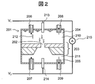
- FIG. 2 shows a configuration of a chamber portion in which the nanopore substrate is disposed, but the substrate does not have the third electrode.
- the chamber 201 is composed of two closed spaces 204 and 205 with a nanopore substrate 203 having nanopores 202 therebetween, and liquids 210 and 211 introduced through inflow paths 206 and 207 and outflow paths 208 and 209. Is filled with.
- the liquids 210 and 211 contain a large amount of ions (hereinafter referred to as ionic liquid) that are responsible for charge, and one of the liquids 210 and 211 contains a small amount of sample 212 to be analyzed and is arranged on both sides of the nanopore.
- ionic liquid is the same as in the present invention, and for example, an aqueous potassium chloride solution is used.
- the sample 212 passes through the nanopore 202, the components of the sample 212 are analyzed by detecting physical, electrical, and chemical interactions between the sample 212 and the nanopore 202.
- the sample 212 passes through the nanopore 202.
- Detecting a phenomenon in which the current value between the electrodes 213 and 214 decreases because the amount of ions passing through the nanopore decreases when it is present than when it is not present in the nanopore 202 (blocking current method). Analyze the sample.
- the frequency at which the sample 212 reaches the opening of the nanopore 202 is small, so the frequency at which the sample 212 detects signals through the nanopore 202 is also small.
- the problem is that the measurement throughput decreases.
- the arrival frequency can be increased by increasing the potential difference.
- the speed at which the sample 212 passes through the nanopore 202 also increases, it is difficult to accurately acquire the signal.
- the sample is DNA or RNA, it is necessary to distinguish adjacent bases at 0.3 to 0.7 nm.
- double-stranded DNA consisting of 1000 1nM bases.
- the frequency is 0.5 to 1 times / second and the passing speed is 1 msec or less.
- a signal corresponding to one base of about 100 pA must be acquired with high-speed sampling of 1 ⁇ sec or less.
- the concentration of the KCl aqueous solution is changed between the liquids 210 and 211 on both sides of the nanopore 202 to create a concentration gradient, and the potential difference in the vicinity of the nanopore opening is increased.
- the concentration is 3.4 mol / L at 20 ° C., and there is a limit to increasing the concentration gradient (M. Wanunu, W. Morrison, Y. Rabin, A. Y. Grosberg, A. Meller, 2009, Nat .Nano, 379).
- the frequency with which the sample passes through the nanopores remains the same, and increasing the number of nanopores in parallel can improve the measurement throughput, but it is difficult to manufacture multiple nanopores in a uniform size. In addition, manufacturing variations may become detection signal variations, and it is difficult to detect with high accuracy.
- the sample is a low-concentration DNA
- PCR method Polymerase Chain Reaction method
- problems with accuracy such as amplification errors and the presence of difficult sites, such as Polymerase It is preferable not to use the PCR method from the problem of high cost because an enzyme is used.
- the third electrode is arranged on the substrate of the chamber portion, and the electrode 114 (first electrode), the electrode 115 (second electrode), and the third electrode are arranged.
- the sample charged biopolymer
- the nanopore passage frequency can be easily improved.
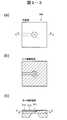
- FIG. 3A shows an embodiment of the substrate used in the present invention.
- FIG. 3A is a plan view of the substrate 301.
- FIG. 3-1 (b) is a cross-sectional view taken along line AA of FIG. 3-1 (c).
- FIG. 3-1 (c) is a cross-sectional view taken along the line II of FIG. 3-1 (a).
- the substrate 301 disposed in the chamber includes a base (base material) 302, a thin film 303, an electrode 304, and an insulating layer 305.
- the thin film of the substrate is provided with nanopores 306 that are nanometer-sized pores.
- the nanopore 306 penetrates the substrate.
- the size of the nanopore 306 is desirably 1 nm to 100 nm.
- the nanopore can be produced by a known method such as a method using a focused ion beam or a method using an electron beam (for example, J. Li, D. Stein et al., 2001, Nature, 412, 166, AJStorm et al., 2003, Nat. Mater. 2, 537540).
- silicon as the base 302
- silicon nitride, silicon oxide, or silicon carbide as the thin film 303
- gold, platinum, tungsten, or tantalum as the electrode 304
- insulation As the layer 305, silicon nitride, silicon oxide, or the like can be advantageously used.
- the substrate 301 preferably has a thickness of 100 ⁇ m to 1,000 ⁇ m.
- the base 302 has a thickness of 100 ⁇ m to 1000 ⁇ m
- the electrode 304 has a thickness of 1 nm to 100 nm
- the insulating layer has a thickness of 5 nm to 50 nm.
- the thickness of the thin film varies depending on the arrangement and number of third electrodes (sample collection electrodes) and measurement electrodes, but in the case of the configuration shown in FIG. 3-1, the thickness of the thin film is 1 nm to 10 nm, preferably 1 nm to 5 nm is preferable.
- the electrode 304 is disposed in the vicinity of the nanopore 306 of the substrate.
- the electrode 304 includes, for example, a portion surrounding the nanopore 306 and a portion that can function as a lead wire for applying a voltage extending from the portion toward the outer edge of the substrate, as shown in FIG. It may be a thing.
- the portion surrounding the nanopore 306 and the portion capable of functioning as a lead wire have a diameter of 10 nm to 1,000 nm and a width of 10 nm to 1,000 nm, respectively.
- the thin film 303 is deposited on the base 302, and the electrode 304 is processed by a selective etching using a pattern or a lift-off process. And a method of processing the nanopore 306 after the insulating layer 305 is deposited.
- the electrode 304 is processed by a selective etching using a pattern or a lift-off process.
- a method of processing the nanopore 306 after the insulating layer 305 is deposited.
- FIG. 3-2 shows another embodiment 307 of the substrate.
- FIG. 3-2 (a) shows a plan view of the substrate 307.
- FIG. FIG. 3-2 (b) is a cross-sectional view taken along line BB of FIG. 3-2 (c).
- FIG. 3-2 (c) is a cross-sectional view taken along the line II-II of FIG. 3-2 (a).
- the shape of the electrode (third electrode) is different from the structure of the substrate shown in FIG. 3-1, and the electrode 308 covers the entire surface of the thin film (except for nanopores) of the substrate. Is formed.
- the electrode 308 can be easily produced by vapor-depositing an electrode member on the entire surface of the substrate. Even when a plurality of nanopores are formed on a thin film, the same voltage can be applied to all nanopores at once by the electrode 308.
- FIG. 3-3 shows another embodiment 309 of the substrate.
- FIG. 3A shows a plan view of the substrate 309.
- FIG. 3-3 (b) is a sectional view taken along the line CC of FIG. 3-3 (c).
- FIG. 3-3 (c) is a cross-sectional view taken along line III-III of FIG. 3-3 (a).
- the structure of the substrate shown in FIG. 3A is different in the shape of the insulating layer.
- the insulating layer is exposed in the space 311 in the vicinity of the nanopore. 312 is formed.
- the space in which the sample can be attracted by the electrode 310 (electric field) is expanded, so that the sample can be easily collected over a wide range.
- 3-4 shows another embodiment 313 of the substrate.
- FIG. 3-4 (a) shows a plan view of the substrate 313.
- FIG. 3-4 (b) is a sectional view taken along the line DD of FIG. 3-4 (c).
- FIG. 3-4 (c) is a cross-sectional view taken along line IV-IV in FIG. 3-4 (a).
- the embodiment shown in FIG. 3-4 is a combination of the embodiment 307 in FIG. 3-2 and the embodiment 309 in FIG. 3-3.
- the electrode 314 is formed on the entire surface of the thin film, and the electrode 314 is formed in the space 315.
- An insulating layer 316 is formed so as to be exposed. This embodiment has the advantages of the embodiment 307 of FIG. 3-2 and the embodiment 309 of FIG. 3-3.
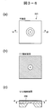
- 3-5 shows another embodiment 317 of the substrate.
- FIG. 3-5 (a) shows a plan view of the substrate 317.
- FIG. FIG. 3-5 (b) is a sectional view taken along line EE of FIG. 3-5 (c).
- FIG. 3-5 (c) is a cross-sectional view taken along line VV of FIG. 3-5 (a).
- the nanopore 318 is formed only on the thin film 319, and the electrode 320 is disposed around the nanopore 318 (that is, around the nanopore).
- a film 319 is deposited on the base 321, and an electrode 320 and an insulating layer 322 are formed on the film 319 in advance by a selective etching using a pattern, a lift-off process, or the like. Then, the nanopore 318 is processed in the thin film 319 by an electron beam or an ion beam.
- the thickness of the film targeted for nanopore processing is thinner, and the material is less likely to be mixed by processing only the thin film than by processing the nanopore on the thin film on which the insulating layer is deposited.
- nanopores are provided only on 319, easy and high-quality processing can be realized.
- FIGS. 3-6 Also shown in FIGS. 3-6 is another embodiment 323 of the substrate.
- FIG. 3-6 (a) shows a plan view of the substrate 323.
- FIG. 3-6 (b) is a sectional view taken along line FF of FIG. 3-6 (c).
- FIG. 3-6 (c) is a cross-sectional view taken along the line VI-VI of FIG. 3-6 (a).
- the embodiment shown in FIG. 3-6 differs from the substrate structure shown in Embodiment 317 in FIG. 3-5 in terms of the shape of the electrode, and the electrode 324 is formed on the entire surface of the thin film except for the portion that is recessed from the end of the nanopore. Is formed.
- FIGS. 3-7 Also shown in FIGS. 3-7 is another embodiment 325 of the substrate.
- FIG. 3-7 (a) shows a plan view of the substrate 325.
- FIG. 3-7 (b) shows a cross-sectional view taken along the line GG of FIG. 3-7 (c).
- FIG. 3-7 (c) is a sectional view taken along line VII-VII in FIG. 3-7 (a).
- the electrodes 327 and 328 around the nanopore 326 in multiple (double). For example, when the sample is negatively charged, the potential V327 applied to the inner electrode 327 and the potential V328 applied to the outer electrode 328 are set to satisfy V327> V328 so that the sample is in the vicinity of the nanopore 326. Can be collected. When the sample is positively charged, a reverse voltage may be applied. When the electrodes are triple and quadruple, it is possible to collect samples from a wider range in the vicinity of the nanopore. Furthermore, by applying a voltage so that V1 ⁇ V328 ⁇ V327 ⁇ V2, the sample collected in the vicinity of the nanopore can be passed through the nanopore with high efficiency.
- 3-8 show another embodiment 329 of the substrate.
- FIG. 3-8 (a) shows a plan view of the substrate 329.
- FIG. FIG. 3-8 (b) is a sectional view taken along line HH of FIG. 3-8 (c).
- FIG. 3-8 (c) is a cross-sectional view taken along line VIII-VIII in FIG. 3-8 (a).
- the embodiment shown in FIG. 3-8 is a method of surrounding electrodes around the nanopore in the same manner as the embodiment of FIG. 3-7.
- the electrodes can be further multilayered.
- the electrodes 330 and 331 have a structure in which electrode members are vapor-deposited on the entire surface of each layer (excluding the part retracted from the end of the nanopore).
- the potential V330 applied to the electrode 330 and the potential V331 applied to the electrode 331 are applied so that V330> V331.
- a reverse voltage may be applied.
- the multilayer arrangement makes it easier to arrange the lead wires on the electrodes.
- the substrate is described as a thin film on the top and the base on the bottom, but when placed in the chamber, the relationship between the top and bottom of the thin film and the base is reversed. It doesn't matter.
- the third electrode is preferably formed on the sample introduction section side.
- the nanopore biopolymer analyzer corresponding to the embodiment of FIG. 3 is separated into two sections with a thin film having one or a plurality of nanometer-size pores open and the thin film, separated from the sample introduction side.
- the first chamber and the second chamber on the sample outflow side, the outflow / inflow path for supplying the liquid to the two sections of the chamber, and the first chamber are provided for applying a voltage across the substrate.
- Near the chamber side of It may be those characterized.
- FIG. 4 shows another embodiment of the present invention.
- FIG. 4 (a) shows a nanopore measurement system 401 describing the chamber portion of the present invention.
- FIG. 4B shows a cross-sectional view taken along the line JJ in which the substrate shown in FIG. 4A is cut vertically in the axial direction of the nanopore 404 at the electrode 409.
- the arrangement of the chamber and the nanopore substrate, the liquid to be used, and the like are the same as those in the embodiment 101 of FIG. 1, but a tunnel current is used as a method of measuring the sample 402, unlike the blocking current of FIG. Therefore, it is preferable to dispose the electrodes 405 and 406 for measuring tunneling current facing the nanopore substrate 403 with the nanopore 404 interposed therebetween.
- a tunnel current flows when the sample 402 exists at a position between the electrodes in the chamber, and the component of the sample can be analyzed from the magnitude of the tunnel current.
- the electrodes 407, 408, and 409 contribute to passing the sample 402 through the nanopore 404.
- the electrode 409 has the function of collecting the sample 402 in the vicinity of the nanopore 404, similar to the electrode 116 of the embodiment 101 of FIG. Fulfill.
- the sample 402 can pass through the nanopore 404 with high frequency, and the measurement throughput can be improved.
- the nanopore-type biopolymer analyzer corresponding to the embodiment of FIG. 4 is separated into two sections with a thin film having one or a plurality of nanometer-size pores open and the thin film, separated from the sample introduction side.
- the first chamber and the second chamber on the sample outflow side, the outflow / inflow path for supplying the liquid to the two sections of the chamber, and the first chamber are provided for applying a voltage across the substrate.
- a thin film in which the arrangement of the third electrode is in the vicinity of the first chamber side of the nanopore opening, and the fourth and fifth electrodes are in the vicinity of the second chamber side or the nanopore is formed. It may be characterized by being inside.
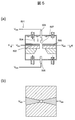
- FIG. 5 shows another embodiment of the present invention.
- FIG. 5 (a) shows a nanopore measurement system 501 describing the chamber portion of the present invention.
- FIG. 5B shows a cross-sectional view taken along the line KK of the substrate shown in FIG. 5A cut vertically in the axial direction of the nanopore at the electrodes 502 and 503.
- the electrodes 502 and 503, which are electrodes for tunnel current measurement, are substituted for the function of collecting the sample performed by the electrode 409 of the embodiment of FIG.
- the component analysis of the sample 504 is also performed by a tunnel current generated between the electrodes 502 and 503.
- the movement of the sample 504 is induced using a potential difference between the electrode 505 and the electrode 506.
- the potentials applied to the electrodes 505, 506, 502, and 503 are V505, V506, V502, and V503, respectively, V505 ⁇ V502 ⁇ V503 ⁇ V506, so that the electrode 505 A force depending on the potential difference acts on the sample 504 between the electrode 505 and the electrode 502 and between the electrode 505 and the electrode 503, and the sample 504 can be collected in the vicinity of the nanopore 507.
- the collected sample 504 is attracted to the electrode 506 and passes through the nanopore 507, and at that time, passes between the electrode 502 and the electrode 503. For this reason, the component of the sample can be measured by detecting a change in tunnel current generated between the electrode 502 and the electrode 503.
- the step of collecting the sample 504 near the nanopore and the step of detecting the components of the sample 504 may be performed separately.
- V505 ⁇ V502 ⁇ V503 and V506 ⁇ V502 ⁇ V503 are set, and in the stage of detecting the sample, a voltage may be applied so that V505 ⁇ V502 ⁇ V503 ⁇ V506.
- the nanopore-type biopolymer analyzer corresponding to the embodiment of FIG. 5 is, for example, a sample that is separated into two sections with a thin film having one or a plurality of nanometer-size pores open and the thin film.
- a fourth electrode a power source for applying a voltage to the electrodes, an amplifier for amplifying an electric signal between the electrodes, an analog-digital converter for converting the analog output of the amplifier into a digital output, and a data logger
- a third and 4 of the electrode may be characterized in that the first chamber side near the nanopore aperture.
- FIG. 6 shows another embodiment of the present invention.
- FIG. 6A shows a nanopore measurement system 601 in which the chamber portion of the present invention is described.
- FIG. 6B is a cross-sectional view taken along line LL in which the substrate shown in FIG. 6A is cut vertically in the axial direction of the nanopore 602 at the electrode 605.
- the measuring electrode 603 is arranged in parallel along the axial direction of the nanopore 602. 604 are arranged.
- the electrode 605 serves to collect the sample 606 in the vicinity of the nanopore 602, similarly to the electrode 409 of the embodiment of FIG.
- the measurement electrodes 603 and 604 are preferably arranged very close to each other.
- the distance between the electrodes 603 and 604 is preferably 0.3 nm to 20 nm, more preferably 5 nm or less, and further preferably 2 nm or less. It is also preferable that an insulating layer separates the electrodes 603 and 604.
- the distance between the electrode 605 that is a sample collection electrode and the measurement electrode 603 is preferably larger than the distance between the electrodes 603 and 604.
- the distance between the electrode 605 and the measurement electrode 603 is, for example, 10 nm or more, more preferably 20 nm or more, and further preferably 30 nm or more.
- a tunnel current corresponding to the component of the sample flows when the sample 606 passes through the nanopore 602.
- the movement of the sample is induced using the potential difference between the electrodes 607, 608, and 605.
- the potentials applied to the electrodes 607, 608, and 605 are V607, V608, and V605, a voltage is applied so that V607 ⁇ V605 ⁇ V608.
- the sample 606 can be passed through the nanopore 602. By increasing the potential difference between V607 and V605, more samples 606 gather near the nanopore 602, and the frequency with which the sample 606 passes through the nanopore 602 increases, thereby improving the measurement throughput.
- the nanopore-type biopolymer analyzer corresponding to the embodiment of FIG. 6 is, for example, a sample that is separated into two sections with a thin film having one or a plurality of nanometer-size pores open and the thin film.
- a voltage is applied to the first electrode disposed in one chamber, the second electrode disposed in the second chamber, the third, fourth, and fifth electrodes disposed in the vicinity of the nanopore.
- a power supply an amplifier that amplifies the electrical signal between the electrodes, an analog-to-digital converter that converts the analog output of the amplifier into a digital output and a data logger, and the arrangement of the third electrode is nanopore Near the first chamber side of the opening
- the fourth and fifth electrodes are in the vicinity of the second chamber side or inside the thin film in which the nanopores are formed, and each electrode is perpendicular to the nanopore axis direction, and the electrodes are parallel to each other. It may be characterized by being arranged.
- FIG. 7 shows another embodiment of the present invention.
- FIG. 7A shows a nanopore measurement system 701 in which the chamber portion of the present invention is described.
- FIG. 7B is a cross-sectional view taken along line MM in which the substrate shown in FIG. 7A is cut vertically in the axial direction of the nanopore at the electrode 702.
- the function of collecting the sample which the electrode 605 of the embodiment of FIG. 6 performed is also replaced by the electrode 702 which is an electrode for tunnel current measurement.
- the component analysis of the sample 703 is also performed using a tunnel current generated between the electrodes 702 and 704.
- the voltages applied to the electrodes 702, 704, 705, and 706 are V702, V704, V705, and V706, respectively, V705 ⁇ V702 ⁇ V704 ⁇ V706.
- the step of collecting the sample 703 and the step of detecting the sample 703 may be separated.
- V705 ⁇ V702 and V706 ⁇ V704 ⁇ V702 are set, and in the stage of detecting the sample, a voltage may be applied so that V705 ⁇ V702 ⁇ V704 ⁇ V706.
- the nanopore type biopolymer analyzer corresponding to the embodiment of FIG. 7 is, for example, a sample that is separated into two sections with a thin film having one or more nanometer-sized pores open and the thin film.
- An amplifier that amplifies an electrical signal between the electrodes, an analog-to-digital converter that converts the analog output of the amplifier into a digital output and a data logger, and the arrangement of the third electrode is the first of the nanopore opening 1 near the chamber side, 4 electrodes are arranged in the vicinity of the second chamber side or inside the thin film in which the nanopores are formed, each electrode is perpendicular to the nanopore axis direction, and the electrodes are arranged in parallel to each other.
- the distance between the electrode and the fourth electrode may be 5 nm or less, for example, 2 nm or less.
- the detection method may be other methods.
- FIG. 8 shows another embodiment of the present invention showing the configuration of the chamber, nanopore, and electrode when analyzing the component of the sample by capacitance measurement.
- FIG. 8 (a) shows a nanopore measurement system 801 describing the chamber portion of the present invention.
- FIG. 8B shows a cross-sectional view of the substrate shown in FIG. 8A taken along the line NN along the electrode 802 perpendicular to the axial direction of the nanopore.
- the electrodes 802, 804, and 805 are arranged in parallel along the axial direction of the nanopore 803, and the electrode 802 faces the nanopore 803 and is arranged in the vicinity of the nanopore.
- the electrode 804 and the electrode 805 are disposed at a position inside the thin film inside the opening of the nanopore 803 closer to the electrode 802, that is, a position closer to the sample outflow section than the electrode 802.
- the distance between the measurement electrode 804 and the electrode 805 is the same as that in the embodiment of FIG. 6 and is preferably arranged very close to each other.
- the distance between the electrodes 804 and 805 is preferably 0.3 nm to 20 nm, more preferably 5 nm or less, and further preferably 2 nm or less. It is also preferable that an insulating layer separates the electrodes 804 and 805.
- the distance between the electrode 802 for sample collection and the electrode for measurement 804 is the same as that in the embodiment of FIG. 6 and is preferably larger than the distance between the electrodes 804 and 805.
- the capacitance can be measured and the components of the sample can be analyzed.
- the electrode 802 functions to collect the sample 806 in the vicinity of the nanopore 803.
- the potential applied to each of the electrodes 802, 807, and 808 is V802, V807, and V808, when the sample is negatively charged, a voltage is applied so that V807 ⁇ V802 ⁇ V808. It can be efficiently passed through the nanopore 803.
- FIG. 9 shows another embodiment of the present invention that uses capacitance measurement.
- FIG. 9A shows a nanopore measurement system 901 describing the chamber portion of the present invention.
- FIG. 9B is a cross-sectional view taken along the line OO of the substrate shown in FIG. 9A cut at the electrode 902 perpendicularly in the axial direction of the nanopore.
- the function of collecting the sample that the electrode 802 of the embodiment of FIG. 8 has collected is replaced by the electrode 902 that is an electrode for capacitance measurement.
- Component analysis of the sample 903 can also be performed by measuring the capacitance between the electrodes 902 and 904. For example, when the sample 903 is negatively charged and the voltages applied to the electrodes 902, 904, 905, and 906 are V902, V905, and V906, respectively, the voltages are applied so that V905 ⁇ V902 ⁇ V906. By doing so, a sample can be collected between the electrode 905 and the electrode 902. Then, the component of the sample 903 can be analyzed by measuring the capacitance between the electrode 902 and the electrode 904.
- the step of collecting the sample 903 and the step of detecting the sample 903 may be performed separately.
- V905 ⁇ V902 and V906 ⁇ V902 are set, and in the stage of detecting the sample, a voltage may be applied so that V905 ⁇ V902 ⁇ V906.
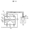
- FIG. 10 shows an example of an embodiment in which a sample is introduced into a chamber in the present invention. Specifically, a nanopore measurement system 1001 in which a chamber part, a sample container, and a flow path of the present invention are described is shown.
- the sample 1003 exists in the sample container 1002, and the sample 1003 can be sucked into the chamber 1004 and further collected near the opening of the nanopore 1005.
- An electrode 1007 may be disposed on the sample container side of the flow path 1006 connecting the sample container 1002 and the chamber 1004 or in the vicinity of the flow path. A voltage is applied between the electrode 1007 and the electrode 1008 disposed in the opening of the nanopore 1005, and the sample 1003 is moved from the sample container 1002 to the opening of the nanopore 1005 by electrophoresis.
- the channel 1006 may be coated to prevent or promote electroosmotic flow according to the charge state of the sample 1003.
- the detection unit 1009 of the sample 1003 is disposed in a region farther from the opening of the nanopore 1005 than the electrode 1008.
- Examples of the detection method include the aforementioned blocking current method, tunneling current method, capacitance method, and a method of detecting physical, electrical, and chemical changes caused by the interaction between the nanopore and the sample.
- the function of moving the sample 1003 included in the electrode 1008 may be replaced with the electrode of the detection unit 1009.
- the detection unit 1009 can be arranged in the vicinity of the opening into which the sample 1003 of the nanopore 1005 is introduced.
- a voltage is applied between the electrode 1010 and the electrode 1011 and a change in current value when the sample 1003 passes through the nanopore 1005 is measured.
- the electrode 1007 moves the sample 1003 from the sample container 1002 to the chamber 1004 and also functions to collect the sample 1003 in the vicinity of the nanopore 1005.
- FIG. 11A shows a nanopore measurement system 1101 in which an analysis chamber unit including a nanopore substrate having a sample collection electrode in the vicinity of a biological nanopore is described as another embodiment of the present invention.
- biological nanopores 1102 made of ⁇ -hemo-lysine or the like are arranged on a lipid bilayer membrane 1103, and the lipid bilayer membrane 1103 is formed on a solid membrane 1104 that can be made of a resin or a material such as a silicon compound. It can be placed in the drilled hole 1105.
- a voltage to the electrode 1106 disposed so as to surround the hole 1105 on the solid film 1104, the sample 1107 is encouraged to gather at the opening of the nanopore 1102.
- a blocking current method can be used for detection as shown in FIG. 11A.
- a voltage is applied to the electrode 1108 and the electrode 1109, and the gap between the electrode 1108 and the electrode 1109 when the sample 1107 passes through the biological nanopore 1102 is detected. What is necessary is just to measure the change of the flowing current value.
- voltages applied to the electrodes 1106, 1108, 1109 are V1106, V1108, V1109, when the sample 1107 is negatively charged, by applying a voltage so that V1108 ⁇ V1106 ⁇ V1109, the electrode 1108 And the electrode 1106 can collect a sample. Further, the component of the sample 1107 may be analyzed by measuring the blocking current generated in the electrodes 1108 and 1109.
- the step of collecting the sample 1107 and the step of detecting the sample 1107 may be performed separately.
- V1108 ⁇ V1106 and V1109 ⁇ V1106 are set, and in the stage of detecting the sample 1107, by setting V1108 ⁇ V1106 ⁇ V1109, the sample can be efficiently passed through the nanopore.
- a biological nanopore is provided directly in a hole of a solid film (thin film), and a nanopore substrate having a sample collection electrode in the vicinity of the nanopore is provided.
- a nanopore measurement system 1101 ′ in which an analysis chamber portion is described is shown.
- a biological nanopore 1102 ′ may be directly disposed in a hole 1105 ′ on a solid membrane 1104 ′ without using a lipid bilayer membrane.
- Biological nanopores should be produced as described in AR Hall; A. Scott; D. Rotem; Kl Mehta; H. Bayley; C. Dekker: ekNat. Nano. 5, 874 (2010) Can do.
- FIG. 12 shows another embodiment 1201 of the present invention using an analysis chamber portion in which a plurality of nanopores having sample collection electrodes are arranged.
- Samples 1203 and 1203 ′ can be collected in the vicinity of each nanopore 1202 and 1202 ′ by the arranged electrodes 1204 and 1204 ′.
- the frequency at which the samples 1203 and 1203 ′ pass through the nanopores 1202 and 1202 ′ can be changed by separately changing the potentials applied to the electrodes 1204 and 1204 ′.
- the detection units 1205 and 1205 ′ for the samples 1203 and 1203 ′ are positioned away from the openings of the nanopores 1202 and 1202 ′ into which the samples 1203 and 1203 ′ are introduced, and the electrodes 1204 and 1204 ′, that is, the electrodes 1204 and 1204 ′. It is preferable to arrange it on the sample outflow compartment side.
- the sample detection method used may be, for example, a blocking current method, a tunnel current method, a capacitance method, or a method for detecting physical, electrical, or chemical changes caused by the interaction between the nanopore and the sample.
- the component of the sample may be detected.
- the samples 1203 and 1203 ′ are passed through the nanopores 1202 and 1202 ′ by applying a voltage to the electrodes 1206, 1206 ′, 1207, and 1207 ′.
- the electrodes 1204 and 1204 ′ may be at the same potential, or may be integrated. In that case, the samples 1203 and 1203 ′ can be collected to the same extent in the vicinity of the respective 1202 and 1202 ′.
- FIG. 12 shows the case where the detection units 1205 and 1205 ′ are of the blocking current method, but in the case of the tunnel current method and the capacitance method, the electrodes 1206, 1206 ′, 1207, and 1207 ′ move the samples 1203 and 1203 ′. Only used and does not contribute to detection. Therefore, the electrode 1206 and the electrode 1206 ′ may be at the same potential or may be integrated. Similarly, the electrode 1207 and the electrode 1207 ′ may be at the same potential or may be integrated.
- the nanopore type biopolymer analyzer of the present invention may have a plurality of the above chamber diagrams. There may be two or more chamber portions, for example, 2 to 10 chamber portions. The plurality of chamber portions may be connected so as to communicate with each other inside the chamber.
- a plurality of electrodes / channels, a plurality of chamber portions, a plurality of nanopores, and a plurality of electrodes indicate a structure in which a plurality of elements are arranged one-dimensionally or two-dimensionally.
- each element is displayed in two, but each element in this embodiment is not limited to two, and the nanopore type biopolymer analyzer has three, four, or individual elements. You may include more.
- a biopolymer analysis method using a nanopore biopolymer analyzer will be described. If the nanopore type biopolymer analyzer according to the present invention as described above is used, a sample, particularly a biopolymer, in a sample solution can be collected in the vicinity of the nanopore with high efficiency, and the nanopore can be passed through with high frequency. . As a result, the analysis efficiency of the biopolymer can be greatly increased, and the time required for analysis can be shortened.
- a sample solution containing a biopolymer is introduced into the sample introduction section of the nanopore biopolymer analyzer.
- the biopolymer may be any polymeric biomolecule.
- the biopolymer may be naturally derived, but may be synthesized, or may be a derivative that does not exist in nature.
- biopolymers include, for example, nucleic acids such as single-stranded DNA (ssDNA) and double-stranded DNA (dsDNA), single-stranded RNA (ssRNA) and double-stranded RNA (dsRNA), DNA and RNA Hybrid nucleic acids, etc .; peptide nucleic acids; proteins, polypeptides (including peptides such as 100-mer or less) such as proteins and polypeptides consisting of D- or L-amino acids; and sugar chains, such as polysaccharides, sugars of glycoproteins It can be a chain or the like, but is not limited thereto.
- nucleic acids such as single-stranded DNA (ssDNA) and double-stranded DNA (dsDNA), single-stranded RNA (ssRNA) and double-stranded RNA (dsRNA), DNA and RNA Hybrid nucleic acids, etc .
- peptide nucleic acids proteins, polypeptides (including peptide
- the concentration of the sample solution containing the biopolymer is not particularly limited, but good analysis is possible even at a low concentration.
- the concentration of the sample solution may be 0.1 nM or more, 0.001 nm or more, 0.01 nM to 1000 nM, preferably 0.01 nM to 1 nM.
- the sample solution containing the biopolymer is stored in the sample introduction section, and the charged biopolymer is drawn to the vicinity of the nanopore opening by generating a potential difference in the vicinity of the nanopore opening by using the voltage applying means. Can be collected. Subsequently, by generating a potential difference between the sample introduction section and the sample outflow section, the biopolymer gathered in the vicinity of the nanopore opening is guided into the nanopore, passed through the nanopore, and drawn to the sample outflow section. be able to.
- voltage application between the electrodes may be performed as described in the above embodiments.
- a sample solution containing a biopolymer is accommodated in the sample introduction section, and a voltage is applied between the third electrode and the first electrode.
- the charged biopolymer can be collected and passed through the nanopore.
- the first, second, and third electrodes are set so that the potential of the third electrode is higher than the potential of the first electrode and equal to or lower than the potential of the second electrode.
- a negatively charged biopolymer may be collected by applying a voltage.
- voltage is applied to the first, second, and third electrodes so that the potential of the third electrode is higher than the potential of the first electrode and equal to or higher than the potential of the second electrode. Is applied, and then the voltage is changed so that the potential of the third electrode is lower than the potential of the second electrode, thereby collecting negatively charged biopolymers and facilitating passage through the nanopores.
- the voltage is preferably changed by a reversible switching means as described above.
- the reversible switching means is, for example, a control device.
- first, second, and third electrodes have a voltage so that the potential of the third electrode is lower than the potential of the first electrode and equal to or higher than the potential of the second electrode. May be applied to collect positively charged biopolymers.
- voltage is applied to the first, second, and third electrodes so that the potential of the third electrode is lower than the potential of the first electrode and equal to or lower than the potential of the second electrode. And then the voltage is changed so that the potential of the third electrode is higher than the potential of the second electrode, thereby collecting positively charged biopolymers and facilitating passage through the nanopores. .
- the biopolymer passing through the nanopore can be measured by the measurement unit of the nanopore biopolymer analyzer.
- a conventionally known nanopore measurement method may be used.
- a detection method such as a blocking current method, a tunnel current method, or a capacitance method can be used.
- detection based on the spectrum of Raman scattered light generated by irradiating the biopolymer with external light may be performed.
- the method of the present invention By using the method of the present invention, not only can a biopolymer be detected, but it can also be quantified, and further, the sequence and composition of each monomer constituting the biopolymer can be analyzed, and a sequence analysis can be performed. it can.
- the method and the analysis apparatus of the present invention are suitable for the analysis of a relatively large size biopolymer that has been difficult to analyze.
- the method and the analysis apparatus of the present invention can be well analyzed, of course, for DNA as short as less than lkb, but preferably 1 kb or more, more preferably 3 kb or more, particularly preferably 4 kb or more, for example 1 to 5 kb. Those of length are particularly suitable for analysis through a nanopore.
- the method of the present invention is also suitable for analyzing low concentrations of biopolymers in a sample solution.
- Nanopore meter System 902 ... Electrode, 903 ... Sample, 904 ... Electrode, 905 ... Electrode, 906 ... Electrode, 1001 ... Nanopore measurement system, 1002 ... Sample container, 1003 ... Sample, 1004 ... Chamber, 1005 ... Nanopore, 1006 ... Channel, 1007 ... Electrode, 1008 ... Electrode, 1009 ... Detection part, 1010 ... Electrode, 1011 ... Electrode, 1101 ... Nanopore measurement system, 1102 ... Biological nanopore, 1103 ... Bilayer lipid, 1104 ... Solid membrane, 1105 ... Hole, 1106 ... Electrode, 1107 ... Sample, 1108 ... Electrode, 1109 ... Electrode , 1201 ...
- Nanopore measurement system 1202 ... Nanopore, 1202 '... Nanopore, 1203 ... Sample, 1203' ... Sample, 1204 ... Electrode, 1204 '... Electrode, 1205 ... Detector, 1205' ... Detector, 1206 ... Electrode, 1206 '... electrode, 1207 ... electrode, 1207' ... electrode
Landscapes
- Health & Medical Sciences (AREA)
- Life Sciences & Earth Sciences (AREA)
- Engineering & Computer Science (AREA)
- Chemical & Material Sciences (AREA)
- Physics & Mathematics (AREA)
- Biomedical Technology (AREA)
- Molecular Biology (AREA)
- Immunology (AREA)
- Analytical Chemistry (AREA)
- Pathology (AREA)
- General Physics & Mathematics (AREA)
- General Health & Medical Sciences (AREA)
- Biochemistry (AREA)
- Food Science & Technology (AREA)
- Medicinal Chemistry (AREA)
- Biophysics (AREA)
- Urology & Nephrology (AREA)
- Spectroscopy & Molecular Physics (AREA)
- Nanotechnology (AREA)
- Hematology (AREA)
- Dispersion Chemistry (AREA)
- Chemical Kinetics & Catalysis (AREA)
- Electrochemistry (AREA)
- Investigating Or Analyzing Materials By The Use Of Electric Means (AREA)
- Investigating Or Analysing Biological Materials (AREA)
Abstract
La présente invention porte sur un dispositif d'analyse de biopolymère à base de nanopore, apte, dans un procédé de mesure utilisant un nanopore, à améliorer une fréquence de passage à laquelle un échantillon à faible concentration passe à travers le nanopore et d'améliorer le débit, et porte également sur un dispositif d'analyse de biopolymère utilisant le dispositif d'analyse de biopolymère à base de nanopore. La présente invention concerne en particulier un dispositif d'analyse de biopolymère à base de nanopore caractérisé par le fait qu'il possède une partie chambre comprenant : une chambre ayant une section d'introduction d'échantillon et une section de flux sortant d'échantillon séparées par un substrat ; une première électrode disposée dans la section d'introduction d'échantillon et une deuxième électrode disposée dans la section de flux sortant d'échantillon ; un film mince formé sur le substrat ; un nanopore disposé dans le film mince formé sur le substrat et reliant à communication la section d'introduction d'échantillon et la section de flux sortant d'échantillon ; une troisième électrode disposée près du nanopore du substrat ; et un moyen d'application de tension pour les électrodes. Dans le dispositif d'analyse de biopolymère à base de nanopore, le moyen d'application de tension comprend un moyen d'application de tensions entre les première et troisième électrodes, entre les première et deuxième électrodes, et entre les troisième et deuxième électrode, respectivement. La présente invention concerne également le procédé d'analyse de biopolymère utilisant le dispositif d'analyse de biopolymère à base de nanopore.
Priority Applications (3)
| Application Number | Priority Date | Filing Date | Title |
|---|---|---|---|
| CN201280038456.6A CN103718029B (zh) | 2011-08-09 | 2012-07-25 | 纳米孔式分析装置 |
| US14/237,176 US10222348B2 (en) | 2011-08-09 | 2012-07-25 | Nanopore-based analysis device |
| EP12822028.2A EP2743690B1 (fr) | 2011-08-09 | 2012-07-25 | Dispositif d'analyse à base de nanopore |
Applications Claiming Priority (2)
| Application Number | Priority Date | Filing Date | Title |
|---|---|---|---|
| JP2011173567A JP5670278B2 (ja) | 2011-08-09 | 2011-08-09 | ナノポア式分析装置 |
| JP2011-173567 | 2011-08-09 |
Publications (1)
| Publication Number | Publication Date |
|---|---|
| WO2013021815A1 true WO2013021815A1 (fr) | 2013-02-14 |
Family
ID=47668330
Family Applications (1)
| Application Number | Title | Priority Date | Filing Date |
|---|---|---|---|
| PCT/JP2012/068765 Ceased WO2013021815A1 (fr) | 2011-08-09 | 2012-07-25 | Dispositif d'analyse à base de nanopore |
Country Status (5)
| Country | Link |
|---|---|
| US (1) | US10222348B2 (fr) |
| EP (1) | EP2743690B1 (fr) |
| JP (1) | JP5670278B2 (fr) |
| CN (1) | CN103718029B (fr) |
| WO (1) | WO2013021815A1 (fr) |
Cited By (14)
| Publication number | Priority date | Publication date | Assignee | Title |
|---|---|---|---|---|
| CN103193189A (zh) * | 2013-02-21 | 2013-07-10 | 东南大学 | 一种用于dna检测的多电极纳米孔装置及其制造方法 |
| EP2908128A1 (fr) * | 2014-02-14 | 2015-08-19 | Ecole Polytechnique Federale de Lausanne (EPFL) | Dispositif de détection moléculaire |
| WO2015121394A1 (fr) * | 2014-02-14 | 2015-08-20 | Ecole Polytechnique Federale De Lausanne (Epfl) | Dispositif de détection moléculaire |
| US20160194698A1 (en) * | 2014-12-16 | 2016-07-07 | Arizona Board Of Regents On Behalf Of Arizona State University | Systems, apparatuses and methods for reading polymer sequence |
| WO2017212647A1 (fr) * | 2016-06-10 | 2017-12-14 | 株式会社日立ハイテクノロジーズ | Procédé et appareil pour l'analyse de biomolécules |
| CN110055168A (zh) * | 2014-04-03 | 2019-07-26 | 意法半导体股份有限公司 | 用于基于纳米通道的核酸测序的设备和方法 |
| CN112567233A (zh) * | 2018-08-28 | 2021-03-26 | 株式会社日立高新技术 | 生物分子分析装置 |
| JP2022523435A (ja) * | 2019-03-12 | 2022-04-22 | オックスフォード ナノポール テクノロジーズ ピーエルシー | ナノ細孔センシングデバイスと操作方法およびその成形方法 |
| US11371980B2 (en) | 2016-10-20 | 2022-06-28 | Hitachi High-Tech Corporation | Method for treating biomolecules and method for analyzing biomolecules |
| US12140563B2 (en) | 2007-12-19 | 2024-11-12 | Oxford Nanopore Technologies Plc | Formation of layers of amphiphilic molecules |
| US12411125B2 (en) | 2020-07-17 | 2025-09-09 | Oxford Nanopore Technologies Plc | Nanopore sensing device |
| US12458945B2 (en) | 2012-10-26 | 2025-11-04 | Oxford Nanopore Technologies Plc | Formation of array of membranes and apparatus therefor |
| US12540937B2 (en) | 2012-02-13 | 2026-02-03 | Oxford Nanopore Technologies Plc | Apparatus for supporting an array of layers of amphiphilic molecules and method of forming an array of layers of amphiphilic molecules |
| US12552661B2 (en) | 2018-05-24 | 2026-02-17 | Oxford Nanopore Technologies Plc | Nanopore array with electrode connectors protected from electrostatic discharge |
Families Citing this family (54)
| Publication number | Priority date | Publication date | Assignee | Title |
|---|---|---|---|---|
| US9194838B2 (en) | 2010-03-03 | 2015-11-24 | Osaka University | Method and device for identifying nucleotide, and method and device for determining nucleotide sequence of polynucleotide |
| KR20150041146A (ko) | 2012-08-17 | 2015-04-15 | 오사카 유니버시티 | 시료의 분석 방법 |
| JP6282036B2 (ja) | 2012-12-27 | 2018-02-21 | クオンタムバイオシステムズ株式会社 | 物質の移動速度の制御方法および制御装置 |
| JP5904958B2 (ja) | 2013-03-07 | 2016-04-20 | 株式会社東芝 | 半導体マイクロ分析チップ及びその製造方法 |
| JP5951527B2 (ja) | 2013-03-07 | 2016-07-13 | 株式会社東芝 | 検体検出装置及び検出方法 |
| US9322820B2 (en) * | 2013-03-14 | 2016-04-26 | Wisconsin Alumni Research Foundation | System and apparatus for nanopore sequencing |
| CA3116407C (fr) * | 2013-03-15 | 2023-02-07 | President And Fellows Of Harvard College | Methode de mouillage de surface |
| JP6151128B2 (ja) | 2013-08-12 | 2017-06-21 | 株式会社東芝 | 半導体マイクロ分析チップ及びその製造方法 |
| EP3047282B1 (fr) | 2013-09-18 | 2019-05-15 | Quantum Biosystems Inc. | Dispositifs, systèmes et procédés de séquençage de biomolécules |
| JP2015077652A (ja) | 2013-10-16 | 2015-04-23 | クオンタムバイオシステムズ株式会社 | ナノギャップ電極およびその製造方法 |
| JP2015099031A (ja) * | 2013-11-18 | 2015-05-28 | 株式会社東芝 | 半導体マイクロ分析チップ及びその製造方法 |
| WO2015079510A1 (fr) * | 2013-11-27 | 2015-06-04 | 株式会社日立製作所 | Dispositif, procédé et trousse de mesure de courant |
| US10724147B2 (en) * | 2013-12-25 | 2020-07-28 | Hitachi, Ltd. | Hole forming method, measuring apparatus and chip set |
| WO2015130781A1 (fr) * | 2014-02-25 | 2015-09-03 | Arizona Board Of Regents Acting For And On Behalf Of Arizona State University | Procédés, appareils et systèmes de stabilisation de dispositifs nano-électroniques en contact avec des solutions |
| JP6189231B2 (ja) * | 2014-02-26 | 2017-08-30 | 株式会社東芝 | 微粒子検査装置と微粒子検査システム及び微粒子検査方法 |
| US10438811B1 (en) | 2014-04-15 | 2019-10-08 | Quantum Biosystems Inc. | Methods for forming nano-gap electrodes for use in nanosensors |
| JP6378924B2 (ja) * | 2014-04-23 | 2018-08-22 | 株式会社日立ハイテクノロジーズ | 核酸分析装置および核酸分析方法 |
| EP3158330B1 (fr) * | 2014-06-19 | 2019-03-06 | The Board of Trustees of The Leland Stanford Junior University | Appareils et procédés pour la détermination d'une charge d'analyte |
| GB201411285D0 (en) * | 2014-06-25 | 2014-08-06 | Prosser Joseph | Sequencer |
| JP6258145B2 (ja) | 2014-07-18 | 2018-01-10 | 株式会社東芝 | 微粒子検査システム及びその駆動方法 |
| CN104789468B (zh) * | 2014-07-22 | 2017-10-20 | 奥克莱流体公司 | 颗粒筛选装置 |
| CN104792845A (zh) * | 2014-08-07 | 2015-07-22 | 中国科学院微电子研究所 | 传感装置 |
| JP6538348B2 (ja) * | 2014-12-26 | 2019-07-03 | 株式会社東芝 | 粒子測定装置 |
| CA2976043A1 (fr) | 2015-02-10 | 2016-10-06 | Multerra Bio, Inc. | Appareils et procedes pour detecter des molecules et de l'energie de liaison |
| WO2016157513A1 (fr) * | 2015-04-03 | 2016-10-06 | 株式会社日立製作所 | Procédé et dispositif permettant d'identifier une quantité d'interaction antigène-anticorps |
| CN107683337B (zh) * | 2015-06-23 | 2021-10-22 | 深圳华大生命科学研究院 | 微孔电极及分析化学物质的方法 |
| JP2017053808A (ja) * | 2015-09-11 | 2017-03-16 | 株式会社東芝 | 半導体分析チップ及び微粒子検査方法 |
| JP6831839B2 (ja) * | 2015-10-14 | 2021-02-17 | エスエフシー フルーイディクス、インコーポレイテッド | 溶液中の電気活性種の存在又は流れを検出する電気信号の測定 |
| JP6667896B2 (ja) * | 2015-11-06 | 2020-03-18 | 国立研究開発法人産業技術総合研究所 | リボ核酸固定化担体及びそれを用いたリボ核酸の分離回収方法 |
| US11333626B2 (en) * | 2016-02-22 | 2022-05-17 | Hitachi, Ltd. | Biological sample analysis chip, biological sample analyzer and biological sample analysis method |
| WO2017149756A1 (fr) * | 2016-03-04 | 2017-09-08 | 株式会社日立製作所 | Dispositif d'analyse de particules et procédé d'analyse de particules |
| KR101868221B1 (ko) * | 2016-03-14 | 2018-06-15 | 고려대학교 산학협력단 | 이온 채널 압력 센서 및 이의 제조방법 |
| US11486873B2 (en) | 2016-03-31 | 2022-11-01 | Ontera Inc. | Multipore determination of fractional abundance of polynucleotide sequences in a sample |
| WO2018081178A1 (fr) | 2016-10-24 | 2018-05-03 | Two Pore Guys, Inc. | Abondance fractionnaire de séquences polynucléotidiques dans un échantillon |
| KR20190075010A (ko) | 2016-04-27 | 2019-06-28 | 퀀텀 바이오시스템즈 가부시키가이샤 | 생체분자의 측정 및 시퀀싱을 위한 시스템 및 방법 |
| EP3464622B1 (fr) * | 2016-05-31 | 2021-04-28 | F. Hoffmann-La Roche AG | Procédés et systèmes de séquençage d'acide nucléique par reconnaissance tunnel |
| JP6592402B2 (ja) * | 2016-06-03 | 2019-10-16 | 株式会社日立ハイテクノロジーズ | 生体分子計測装置 |
| US10444179B2 (en) | 2016-08-10 | 2019-10-15 | Multerra Bio, Inc. | Apparatuses and methods for detecting molecules and binding energy |
| JP2018048950A (ja) * | 2016-09-23 | 2018-03-29 | 株式会社東芝 | 分析チップ |
| EP3532843B1 (fr) * | 2016-10-26 | 2020-11-18 | F. Hoffmann-La Roche AG | Encapsulation multi-puce de circuits intégrés et cellules d'écoulement pour séquençage nanopore |
| JP6730171B2 (ja) * | 2016-12-07 | 2020-07-29 | 株式会社日立製作所 | 液槽形成方法,測定装置及び分析デバイス |
| JP6846309B2 (ja) * | 2017-08-09 | 2021-03-24 | 株式会社日立製作所 | 溶液槽デバイス |
| US20190094179A1 (en) * | 2017-09-22 | 2019-03-28 | Applied Materials, Inc. | Method for simple fluidic addressing of a nanopore |
| JP6959121B2 (ja) * | 2017-12-05 | 2021-11-02 | 株式会社日立ハイテク | 孔形成方法及び孔形成装置 |
| JP6739121B2 (ja) * | 2018-04-19 | 2020-08-12 | ティーイーアイソリューションズ株式会社 | 分析装置 |
| JP7051632B2 (ja) | 2018-07-30 | 2022-04-11 | 浜松ホトニクス株式会社 | 試料支持体、試料のイオン化方法、及び質量分析方法 |
| US11175260B2 (en) * | 2018-10-30 | 2021-11-16 | International Business Machines Corporation | Adjusting nanopore diameter in situ for molecule characterization |
| JP2020076720A (ja) * | 2018-11-09 | 2020-05-21 | 地方独立行政法人神奈川県立産業技術総合研究所 | 計測装置 |
| JP7162283B2 (ja) * | 2019-05-27 | 2022-10-28 | 国立大学法人山形大学 | 脂質二分子膜チャネル評価チップ及びその製造方法並びに評価装置 |
| CN114846130A (zh) * | 2019-12-03 | 2022-08-02 | 国立研究开发法人科学技术振兴机构 | 纳米孔结构体及包含纳米孔结构体的碱基序列分析装置 |
| US20230103446A1 (en) * | 2020-04-10 | 2023-04-06 | Hewlett-Packard Development Company, L.P. | Microfluidic nanopore sensing devices |
| JP2020153996A (ja) * | 2020-05-29 | 2020-09-24 | 株式会社東芝 | 分析チップ |
| WO2022059698A1 (fr) * | 2020-09-16 | 2022-03-24 | 国立大学法人大阪大学 | Système et procédé spectroscopiques |
| WO2023021627A1 (fr) | 2021-08-18 | 2023-02-23 | 株式会社日立ハイテク | Dispositif d'analyse d'échantillons biologiques |
Citations (8)
| Publication number | Priority date | Publication date | Assignee | Title |
|---|---|---|---|---|
| JP2004233353A (ja) * | 2003-01-31 | 2004-08-19 | Agilent Technol Inc | ナノポアを介するバイオポリマーの転位を制御するための装置及び方法 |
| JP2004233356A (ja) * | 2003-01-27 | 2004-08-19 | Agilent Technol Inc | ナノポアを通って移動するバイオポリマーの識別装置及び方法 |
| JP2005257687A (ja) * | 2004-03-10 | 2005-09-22 | Agilent Technol Inc | トンネルコンダクタンスの変化を検出することによってポリマーをシーケンシングするための方法及び装置 |
| JP2006113057A (ja) * | 2004-10-05 | 2006-04-27 | Agilent Technol Inc | ナノポア分離装置及びその使用方法 |
| JP2008536124A (ja) * | 2005-04-06 | 2008-09-04 | ザ プレジデント アンド フェロウズ オブ ハーバード カレッジ | カーボンナノチューブコントロールを用いる分子特性解析 |
| JP2010230614A (ja) * | 2009-03-30 | 2010-10-14 | Hitachi High-Technologies Corp | ナノポアを用いたバイオポリマー決定方法、システム、及びキット |
| JP2011501806A (ja) * | 2007-10-02 | 2011-01-13 | プレジデント アンド フェロウズ オブ ハーバード カレッジ | ナノポアによる分子の捕捉、再捕捉およびトラッピング |
| JP2011173567A (ja) | 2010-02-25 | 2011-09-08 | Toyota Motor Corp | 車両のシール構造及び車両用ドア |
Family Cites Families (13)
| Publication number | Priority date | Publication date | Assignee | Title |
|---|---|---|---|---|
| EP2383776B1 (fr) * | 1999-06-22 | 2015-02-25 | President and Fellows of Harvard College | Dispositif de nanopore à corps solide pour l'évaluation de biopolymères |
| US7250115B2 (en) * | 2003-06-12 | 2007-07-31 | Agilent Technologies, Inc | Nanopore with resonant tunneling electrodes |
| US8563237B2 (en) * | 2004-09-30 | 2013-10-22 | Agilent Technologies, Inc. | Biopolymer resonant tunneling with a gate voltage source |
| US20070020146A1 (en) * | 2005-06-29 | 2007-01-25 | Young James E | Nanopore structure and method using an insulating substrate |
| US8123922B2 (en) * | 2006-09-07 | 2012-02-28 | University Of Utah Research Foundation | Nanopore based ion-selective electrodes |
| US8003319B2 (en) * | 2007-02-02 | 2011-08-23 | International Business Machines Corporation | Systems and methods for controlling position of charged polymer inside nanopore |
| WO2009035647A1 (fr) * | 2007-09-12 | 2009-03-19 | President And Fellows Of Harvard College | Capteur moléculaire haute résolution en feuille de carbone avec ouverture dans la couche de feuille de carbone |
| US20100122907A1 (en) * | 2008-05-06 | 2010-05-20 | Government of the United States of America, | Single molecule mass or size spectrometry in solution using a solitary nanopore |
| WO2010111605A2 (fr) * | 2009-03-27 | 2010-09-30 | Nabsys, Inc. | La présente invention concerne des dispositifs et des procédés d'analyse de biomolécules et des sondes liées à celles-ci |
| US8986928B2 (en) | 2009-04-10 | 2015-03-24 | Pacific Biosciences Of California, Inc. | Nanopore sequencing devices and methods |
| CN102095768B (zh) * | 2010-11-16 | 2014-07-09 | 浙江大学 | 一种亚纳米厚度的纳米孔传感器 |
| KR101715355B1 (ko) * | 2010-11-30 | 2017-03-13 | 삼성전자주식회사 | 그래핀 전자 소자 |
| US8852407B2 (en) * | 2011-01-28 | 2014-10-07 | International Business Machines Corporation | Electron beam sculpting of tunneling junction for nanopore DNA sequencing |
-
2011
- 2011-08-09 JP JP2011173567A patent/JP5670278B2/ja not_active Expired - Fee Related
-
2012
- 2012-07-25 CN CN201280038456.6A patent/CN103718029B/zh active Active
- 2012-07-25 EP EP12822028.2A patent/EP2743690B1/fr not_active Not-in-force
- 2012-07-25 US US14/237,176 patent/US10222348B2/en active Active
- 2012-07-25 WO PCT/JP2012/068765 patent/WO2013021815A1/fr not_active Ceased
Patent Citations (8)
| Publication number | Priority date | Publication date | Assignee | Title |
|---|---|---|---|---|
| JP2004233356A (ja) * | 2003-01-27 | 2004-08-19 | Agilent Technol Inc | ナノポアを通って移動するバイオポリマーの識別装置及び方法 |
| JP2004233353A (ja) * | 2003-01-31 | 2004-08-19 | Agilent Technol Inc | ナノポアを介するバイオポリマーの転位を制御するための装置及び方法 |
| JP2005257687A (ja) * | 2004-03-10 | 2005-09-22 | Agilent Technol Inc | トンネルコンダクタンスの変化を検出することによってポリマーをシーケンシングするための方法及び装置 |
| JP2006113057A (ja) * | 2004-10-05 | 2006-04-27 | Agilent Technol Inc | ナノポア分離装置及びその使用方法 |
| JP2008536124A (ja) * | 2005-04-06 | 2008-09-04 | ザ プレジデント アンド フェロウズ オブ ハーバード カレッジ | カーボンナノチューブコントロールを用いる分子特性解析 |
| JP2011501806A (ja) * | 2007-10-02 | 2011-01-13 | プレジデント アンド フェロウズ オブ ハーバード カレッジ | ナノポアによる分子の捕捉、再捕捉およびトラッピング |
| JP2010230614A (ja) * | 2009-03-30 | 2010-10-14 | Hitachi High-Technologies Corp | ナノポアを用いたバイオポリマー決定方法、システム、及びキット |
| JP2011173567A (ja) | 2010-02-25 | 2011-09-08 | Toyota Motor Corp | 車両のシール構造及び車両用ドア |
Non-Patent Citations (13)
| Title |
|---|
| A. R. HALL; A. SCOTT; D. ROTEM; K. L MEHTA; H. BAYLEY; C. DEKKER, NAT. NANO., vol. 5, 2010, pages 874 |
| A.J. STORM ET AL., NAT. MATER., vol. 2, 2003, pages 537 - 540 |
| D. FOLOGEA; M. GERSHOW; B. LEDDEN; D. S. MCNABB; J. A. GOLVCHENKO; J. LI, NANO LETT, vol. 5, no. 10, 2005, pages 1905 |
| G. SIGALOV; J. COMER; G. TIMP; A. AKSIMENTIEV, NANO LETT, vol. 8, no. 1, 2008, pages 56 |
| J. LI; D. STEIN ET AL., NATURE, vol. 412, 2001, pages 166 |
| KASIANOWICZ J.J.; BRANDIN E.; BRANTON D.; DEAMER D. W., PROC. NATL. ACAD. SCI. U.S.A., vol. 93, 1996, pages 13770 - 13773 |
| LI J.; D. STEIN; C. MCMULLAN; D. BRANTON; M. J. AZIZ; J. A. GOLOVCHENKO J. A., NATURE, vol. 412, 2001, pages 166 |
| M. TANIGUCHI; M. TSUTSUI; K. YOKOTA; T. KAWAI, APPL PHYS LETT, vol. 95, 2009, pages 123701 |
| M. WANUNU; W. MORRISON; Y. RABIN; A.Y. GROSBERG; A. MELLER, NAT. NANO, vol. 5, 2009, pages 160 |
| M. ZWOLAK; M. D. VENTRA, NANO LETT, vol. 5, no. 3, 2005, pages 421 |
| M.WANUNU; W. MORRISON; Y. RABIN; A.V. GROSBERG; A. MELLER, NAT. NANO, 2009, pages 379 |
| See also references of EP2743690A4 |
| STORM A. J.; J. H. CHEN; X. S. LING; H. ZANDBERGEN; C. DEKKER, NAT. MATER., vol. 2, 2003, pages 537540 |
Cited By (20)
| Publication number | Priority date | Publication date | Assignee | Title |
|---|---|---|---|---|
| US12140563B2 (en) | 2007-12-19 | 2024-11-12 | Oxford Nanopore Technologies Plc | Formation of layers of amphiphilic molecules |
| US12540937B2 (en) | 2012-02-13 | 2026-02-03 | Oxford Nanopore Technologies Plc | Apparatus for supporting an array of layers of amphiphilic molecules and method of forming an array of layers of amphiphilic molecules |
| US12458945B2 (en) | 2012-10-26 | 2025-11-04 | Oxford Nanopore Technologies Plc | Formation of array of membranes and apparatus therefor |
| CN103193189A (zh) * | 2013-02-21 | 2013-07-10 | 东南大学 | 一种用于dna检测的多电极纳米孔装置及其制造方法 |
| US10648965B2 (en) | 2014-02-14 | 2020-05-12 | École Polytechnique Fédérale De Lausanne (Epfl) | Molecular sensing device |
| EP2908128A1 (fr) * | 2014-02-14 | 2015-08-19 | Ecole Polytechnique Federale de Lausanne (EPFL) | Dispositif de détection moléculaire |
| WO2015121394A1 (fr) * | 2014-02-14 | 2015-08-20 | Ecole Polytechnique Federale De Lausanne (Epfl) | Dispositif de détection moléculaire |
| CN110055168A (zh) * | 2014-04-03 | 2019-07-26 | 意法半导体股份有限公司 | 用于基于纳米通道的核酸测序的设备和方法 |
| CN110055168B (zh) * | 2014-04-03 | 2023-02-17 | 意法半导体股份有限公司 | 用于基于纳米通道的核酸测序的设备和方法 |
| US20160194698A1 (en) * | 2014-12-16 | 2016-07-07 | Arizona Board Of Regents On Behalf Of Arizona State University | Systems, apparatuses and methods for reading polymer sequence |
| GB2565954A (en) * | 2016-06-10 | 2019-02-27 | Hitachi High Tech Corp | Method and apparatus for analyzing biomolecules |
| WO2017212647A1 (fr) * | 2016-06-10 | 2017-12-14 | 株式会社日立ハイテクノロジーズ | Procédé et appareil pour l'analyse de biomolécules |
| GB2565954B (en) * | 2016-06-10 | 2022-09-07 | Hitachi High Tech Corp | Method and apparatus for analyzing biomolecules |
| US11371980B2 (en) | 2016-10-20 | 2022-06-28 | Hitachi High-Tech Corporation | Method for treating biomolecules and method for analyzing biomolecules |
| US12552661B2 (en) | 2018-05-24 | 2026-02-17 | Oxford Nanopore Technologies Plc | Nanopore array with electrode connectors protected from electrostatic discharge |
| CN112567233A (zh) * | 2018-08-28 | 2021-03-26 | 株式会社日立高新技术 | 生物分子分析装置 |
| JP7492200B2 (ja) | 2019-03-12 | 2024-05-29 | オックスフォード ナノポール テクノロジーズ ピーエルシー | ナノ細孔センシングデバイスと操作方法およびその成形方法 |
| US12392766B2 (en) | 2019-03-12 | 2025-08-19 | Oxford Nanopore Technologies Plc | Nanopore sensing device, components and method of operation |
| JP2022523435A (ja) * | 2019-03-12 | 2022-04-22 | オックスフォード ナノポール テクノロジーズ ピーエルシー | ナノ細孔センシングデバイスと操作方法およびその成形方法 |
| US12411125B2 (en) | 2020-07-17 | 2025-09-09 | Oxford Nanopore Technologies Plc | Nanopore sensing device |
Also Published As
| Publication number | Publication date |
|---|---|
| EP2743690B1 (fr) | 2017-09-13 |
| CN103718029B (zh) | 2015-07-01 |
| JP5670278B2 (ja) | 2015-02-18 |
| US10222348B2 (en) | 2019-03-05 |
| CN103718029A (zh) | 2014-04-09 |
| US20140158540A1 (en) | 2014-06-12 |
| EP2743690A1 (fr) | 2014-06-18 |
| EP2743690A4 (fr) | 2015-04-01 |
| JP2013036865A (ja) | 2013-02-21 |
Similar Documents
| Publication | Publication Date | Title |
|---|---|---|
| JP5670278B2 (ja) | ナノポア式分析装置 | |
| Rhee et al. | Nanopore sequencing technology: nanopore preparations | |
| Yamazaki et al. | Photothermally assisted thinning of silicon nitride membranes for ultrathin asymmetric nanopores | |
| Tahvildari et al. | Integrating nanopore sensors within microfluidic channel arrays using controlled breakdown | |
| JP2013090576A (ja) | 核酸分析デバイス及びそれを用いた核酸分析装置 | |
| Healy et al. | Solid-state nanopore technologies for nanopore-based DNA analysis | |
| Fu et al. | Nanopore electrochemistry: a nexus for molecular control of electron transfer reactions | |
| Liu et al. | Atomically thin molybdenum disulfide nanopores with high sensitivity for DNA translocation | |
| JP7254366B2 (ja) | ナノポア装置およびその製造方法 | |
| Venta et al. | Differentiation of short, single-stranded DNA homopolymers in solid-state nanopores | |
| Roman et al. | Functionalized solid-state nanopore integrated in a reusable microfluidic device for a better stability and nanoparticle detection | |
| US8409410B2 (en) | Conductivity sensor device comprising diamond film with at least one nanopore or micropore | |
| US11673136B2 (en) | Nanopore devices for sensing biomolecules | |
| Kudr et al. | Fabrication of solid‐state nanopores and its perspectives | |
| JP6579948B2 (ja) | 生体ポリマを分析するための測定試薬及び分析デバイス | |
| US20120267729A1 (en) | Self-sealed fluidic channels for nanopore array | |
| CN105368938B (zh) | 一种基于电击穿在氮化硅薄膜上精确制备纳米孔的方法 | |
| Cadinu et al. | Individually addressable multi-nanopores for single-molecule targeted operations | |
| ITRM20110252A1 (it) | Metodo di analisi di singola molecola mediante rilevazione delle collisioni di una molecola target su nanopori funzionalizzati. | |
| Xu et al. | Controllable shrinking of glass capillary nanopores down to sub-10 nm by wet-chemical silanization for signal-enhanced DNA translocation | |
| Lin et al. | Nanopore confinement for electrochemical sensing at the single-molecule level | |
| KR20140021245A (ko) | 티올기를 갖는 물질이 부착된 금층을 포함한 나노포어를 갖는 장치를 제조하는 방법 및 그를 이용한 핵산 분석 방법 | |
| US20250067722A1 (en) | Devices for single-molecule sequencing, including related methods and processes | |
| Rosenstein et al. | Single‐molecule bioelectronics | |
| Wei et al. | Nanopore-based sensors for DNA sequencing: a review |
Legal Events
| Date | Code | Title | Description |
|---|---|---|---|
| 121 | Ep: the epo has been informed by wipo that ep was designated in this application |
Ref document number: 12822028 Country of ref document: EP Kind code of ref document: A1 |
|
| REEP | Request for entry into the european phase |
Ref document number: 2012822028 Country of ref document: EP |
|
| WWE | Wipo information: entry into national phase |
Ref document number: 2012822028 Country of ref document: EP |
|
| WWE | Wipo information: entry into national phase |
Ref document number: 14237176 Country of ref document: US |
|
| NENP | Non-entry into the national phase |
Ref country code: DE |