WO2013027712A1 - 整流装置、トランジスタおよび整流方法 - Google Patents
整流装置、トランジスタおよび整流方法 Download PDFInfo
- Publication number
- WO2013027712A1 WO2013027712A1 PCT/JP2012/071025 JP2012071025W WO2013027712A1 WO 2013027712 A1 WO2013027712 A1 WO 2013027712A1 JP 2012071025 W JP2012071025 W JP 2012071025W WO 2013027712 A1 WO2013027712 A1 WO 2013027712A1
- Authority
- WO
- WIPO (PCT)
- Prior art keywords
- magnetic field
- electrons
- dimensional channel
- spin
- external magnetic
- Prior art date
- Legal status (The legal status is an assumption and is not a legal conclusion. Google has not performed a legal analysis and makes no representation as to the accuracy of the status listed.)
- Ceased
Links
Images



Classifications
-
- H—ELECTRICITY
- H10—SEMICONDUCTOR DEVICES; ELECTRIC SOLID-STATE DEVICES NOT OTHERWISE PROVIDED FOR
- H10N—ELECTRIC SOLID-STATE DEVICES NOT OTHERWISE PROVIDED FOR
- H10N52/00—Hall-effect devices
- H10N52/101—Semiconductor Hall-effect devices
-
- B—PERFORMING OPERATIONS; TRANSPORTING
- B82—NANOTECHNOLOGY
- B82Y—SPECIFIC USES OR APPLICATIONS OF NANOSTRUCTURES; MEASUREMENT OR ANALYSIS OF NANOSTRUCTURES; MANUFACTURE OR TREATMENT OF NANOSTRUCTURES
- B82Y10/00—Nanotechnology for information processing, storage or transmission, e.g. quantum computing or single electron logic
-
- H—ELECTRICITY
- H01—ELECTRIC ELEMENTS
- H01F—MAGNETS; INDUCTANCES; TRANSFORMERS; SELECTION OF MATERIALS FOR THEIR MAGNETIC PROPERTIES
- H01F10/00—Thin magnetic films, e.g. of one-domain structure
-
- H—ELECTRICITY
- H10—SEMICONDUCTOR DEVICES; ELECTRIC SOLID-STATE DEVICES NOT OTHERWISE PROVIDED FOR
- H10B—ELECTRONIC MEMORY DEVICES
- H10B61/00—Magnetic memory devices, e.g. magnetoresistive RAM [MRAM] devices
-
- H—ELECTRICITY
- H10—SEMICONDUCTOR DEVICES; ELECTRIC SOLID-STATE DEVICES NOT OTHERWISE PROVIDED FOR
- H10D—INORGANIC ELECTRIC SEMICONDUCTOR DEVICES
- H10D48/00—Individual devices not covered by groups H10D1/00 - H10D44/00
- H10D48/385—Devices using spin-polarised carriers
-
- H—ELECTRICITY
- H10—SEMICONDUCTOR DEVICES; ELECTRIC SOLID-STATE DEVICES NOT OTHERWISE PROVIDED FOR
- H10D—INORGANIC ELECTRIC SEMICONDUCTOR DEVICES
- H10D48/00—Individual devices not covered by groups H10D1/00 - H10D44/00
- H10D48/40—Devices controlled by magnetic fields
-
- H—ELECTRICITY
- H10—SEMICONDUCTOR DEVICES; ELECTRIC SOLID-STATE DEVICES NOT OTHERWISE PROVIDED FOR
- H10D—INORGANIC ELECTRIC SEMICONDUCTOR DEVICES
- H10D62/00—Semiconductor bodies, or regions thereof, of devices having potential barriers
- H10D62/80—Semiconductor bodies, or regions thereof, of devices having potential barriers characterised by the materials
- H10D62/81—Semiconductor bodies, or regions thereof, of devices having potential barriers characterised by the materials of structures exhibiting quantum-confinement effects, e.g. single quantum wells; of structures having periodic or quasi-periodic potential variation
- H10D62/812—Single quantum well structures
- H10D62/813—Quantum wire structures
-
- H—ELECTRICITY
- H10—SEMICONDUCTOR DEVICES; ELECTRIC SOLID-STATE DEVICES NOT OTHERWISE PROVIDED FOR
- H10D—INORGANIC ELECTRIC SEMICONDUCTOR DEVICES
- H10D64/00—Electrodes of devices having potential barriers
- H10D64/20—Electrodes characterised by their shapes, relative sizes or dispositions
- H10D64/27—Electrodes not carrying the current to be rectified, amplified, oscillated or switched, e.g. gates
- H10D64/311—Gate electrodes for field-effect devices
- H10D64/411—Gate electrodes for field-effect devices for FETs
- H10D64/511—Gate electrodes for field-effect devices for FETs for IGFETs
- H10D64/512—Disposition of the gate electrodes, e.g. buried gates
-
- H—ELECTRICITY
- H10—SEMICONDUCTOR DEVICES; ELECTRIC SOLID-STATE DEVICES NOT OTHERWISE PROVIDED FOR
- H10N—ELECTRIC SOLID-STATE DEVICES NOT OTHERWISE PROVIDED FOR
- H10N50/00—Galvanomagnetic devices
- H10N50/10—Magnetoresistive devices
-
- H—ELECTRICITY
- H10—SEMICONDUCTOR DEVICES; ELECTRIC SOLID-STATE DEVICES NOT OTHERWISE PROVIDED FOR
- H10N—ELECTRIC SOLID-STATE DEVICES NOT OTHERWISE PROVIDED FOR
- H10N50/00—Galvanomagnetic devices
- H10N50/80—Constructional details
- H10N50/85—Materials of the active region
-
- H—ELECTRICITY
- H10—SEMICONDUCTOR DEVICES; ELECTRIC SOLID-STATE DEVICES NOT OTHERWISE PROVIDED FOR
- H10D—INORGANIC ELECTRIC SEMICONDUCTOR DEVICES
- H10D30/00—Field-effect transistors [FET]
- H10D30/40—FETs having zero-dimensional [0D], one-dimensional [1D] or two-dimensional [2D] charge carrier gas channels
- H10D30/43—FETs having zero-dimensional [0D], one-dimensional [1D] or two-dimensional [2D] charge carrier gas channels having one-dimensional [1D] charge carrier gas channels, e.g. quantum wire FETs or transistors having 1D quantum-confined channels
-
- H—ELECTRICITY
- H10—SEMICONDUCTOR DEVICES; ELECTRIC SOLID-STATE DEVICES NOT OTHERWISE PROVIDED FOR
- H10D—INORGANIC ELECTRIC SEMICONDUCTOR DEVICES
- H10D30/00—Field-effect transistors [FET]
- H10D30/40—FETs having zero-dimensional [0D], one-dimensional [1D] or two-dimensional [2D] charge carrier gas channels
- H10D30/47—FETs having zero-dimensional [0D], one-dimensional [1D] or two-dimensional [2D] charge carrier gas channels having two-dimensional [2D] charge carrier gas channels, e.g. nanoribbon FETs or high electron mobility transistors [HEMT]
- H10D30/471—High electron mobility transistors [HEMT] or high hole mobility transistors [HHMT]
- H10D30/473—High electron mobility transistors [HEMT] or high hole mobility transistors [HHMT] having confinement of carriers by multiple heterojunctions, e.g. quantum well HEMT
- H10D30/4732—High electron mobility transistors [HEMT] or high hole mobility transistors [HHMT] having confinement of carriers by multiple heterojunctions, e.g. quantum well HEMT using Group III-V semiconductor material
-
- H—ELECTRICITY
- H10—SEMICONDUCTOR DEVICES; ELECTRIC SOLID-STATE DEVICES NOT OTHERWISE PROVIDED FOR
- H10D—INORGANIC ELECTRIC SEMICONDUCTOR DEVICES
- H10D62/00—Semiconductor bodies, or regions thereof, of devices having potential barriers
- H10D62/10—Shapes, relative sizes or dispositions of the regions of the semiconductor bodies; Shapes of the semiconductor bodies
- H10D62/117—Shapes of semiconductor bodies
- H10D62/118—Nanostructure semiconductor bodies
- H10D62/119—Nanowire, nanosheet or nanotube semiconductor bodies
- H10D62/121—Nanowire, nanosheet or nanotube semiconductor bodies oriented parallel to substrates
-
- H—ELECTRICITY
- H10—SEMICONDUCTOR DEVICES; ELECTRIC SOLID-STATE DEVICES NOT OTHERWISE PROVIDED FOR
- H10D—INORGANIC ELECTRIC SEMICONDUCTOR DEVICES
- H10D62/00—Semiconductor bodies, or regions thereof, of devices having potential barriers
- H10D62/80—Semiconductor bodies, or regions thereof, of devices having potential barriers characterised by the materials
- H10D62/82—Heterojunctions
- H10D62/824—Heterojunctions comprising only Group III-V materials heterojunctions, e.g. GaN/AlGaN heterojunctions
-
- H—ELECTRICITY
- H10—SEMICONDUCTOR DEVICES; ELECTRIC SOLID-STATE DEVICES NOT OTHERWISE PROVIDED FOR
- H10D—INORGANIC ELECTRIC SEMICONDUCTOR DEVICES
- H10D8/00—Diodes
Definitions
- the present invention relates to a rectifying device, a transistor, and a rectifying method, and more particularly, to a rectifying device, a transistor, and a rectifying method using spin orbit interaction.
- Non-Patent Document 1 proposes a spin field effect transistor utilizing an effective magnetic field caused by spin-orbit interaction. In such a spin electronics field, a spin injector having a high spin polarization is required.
- An object of the present invention is to provide a rectifying device and a rectifying method in which electrons having a high spin polarization rate are obtained when electrons are caused to flow in one direction but electrons are not flowed in the opposite direction, and a transistor using them. To do.
- the present invention provides a one-dimensional channel made of a semiconductor in which electrons travel, and an electric field applied to the one-dimensional channel so that the electrons have an effective magnetic field caused by spin-orbit interaction on the electrons traveling in the one-dimensional channel.
- a rectifier comprising: an electrode that is generated in a direction intersecting a traveling direction; and an external magnetic field generation unit that generates an external magnetic field in the one-dimensional channel. According to the present invention, it is possible to provide a rectifying device in which electrons having a high spin polarization rate are obtained when electrons are caused to flow in one direction, but electrons are not flowed in the opposite direction.
- the one-dimensional channel may be a quantum point contact.
- the external magnetic field generation unit may generate the external magnetic field in a direction of the effective magnetic field or in a direction opposite to the effective magnetic field.
- the one-dimensional channel may have a zinc blende type crystal structure.
- the one-dimensional channel may be formed on the (001) plane or the (110) plane.
- the one-dimensional channel may be a semiconductor formed in a portion constricted from both sides in the direction in which the electrons travel.
- a side gate for forming a depletion layer on both sides of the constricted portion of the one-dimensional channel can be provided.
- the present invention is a transistor including the rectifier.
- a source for injecting electrons into the one-dimensional channel and a drain for receiving electrons from the one-dimensional channel may be provided, and the electrode may be a gate electrode.
- the electrons by applying an electric field to a one-dimensional channel made of a semiconductor and traveling with electrons, the electrons travel an effective magnetic field caused by spin-orbit interaction with the electrons traveling on the one-dimensional channel. And generating the external magnetic field in the one-dimensional channel. According to the present invention, it is possible to provide a rectification method in which electrons with high spin polarization are obtained when electrons are caused to flow in one direction, but electrons do not flow in the opposite direction.
- the present invention it is possible to provide a rectifying device and a rectifying method in which electrons having a high spin polarization rate are obtained when electrons are caused to flow in one direction but electrons are not flowed in the opposite direction, and a transistor using them. it can.
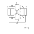
- FIG. 1A is a top view of the rectifier according to the first embodiment
- FIG. 1B is a cross-sectional view taken along line XX of FIG. 1A
- FIG. 1C is a cross-sectional view of FIG. It is a YY sectional view
- FIG. 2 is a schematic plan view of the rectifier according to the first embodiment.
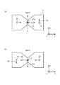
- FIG. 3A and FIG. 3B are diagrams illustrating an effective magnetic field applied to electrons traveling through the quantum point contact.
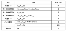
- FIG. 4 is a diagram showing a sample semiconductor stacked structure.
- FIG. 5A shows the conductance between the source and the drain with respect to the side gate voltage
- FIG. 5B shows the spin polarization with respect to the side gate voltage.
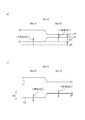
- FIGS. 7A and 7B are schematic diagrams of spin splitting levels depending on the traveling direction of electrons.
- FIG. 8A and FIG. 8B are diagrams for explaining the principle of the transistor according to the second embodiment.
- FIGS. 9A and 9B are schematic diagrams of spin splitting levels depending on the traveling direction of electrons.
- FIG. 10A and FIG. 10B are schematic plan views for explaining the operation of the third embodiment.
- FIG. 1A is a top view of the rectifier according to the first embodiment
- FIG. 1B is a cross-sectional view taken along line XX of FIG. 1A
- FIG. 1C is a cross-sectional view of FIG. It is a YY sectional view.
- a barrier layer 12, a well layer 14, and a barrier layer 16 are sequentially formed as a semiconductor layer 11 on a (001) plane semiconductor substrate 10.
- a groove 30 reaching the substrate 10 is formed in the semiconductor layer 11.
- By making the band gap of the well layer 14 smaller than that of the barrier layers 12 and 16 electrons can be confined in the vicinity of the well layer 14.
- a two-dimensional channel is formed in the well layer 14.
- a source 20 and a drain 22 are formed so as to be in contact with the well layer 14.
- the groove 30 is formed in a V shape from both side surfaces of the semiconductor layer 11 so that a one-dimensional channel 18 through which electrons traveling from the source 20 to the drain 22 pass is formed. Thereby, a constriction is formed in the semiconductor layer 11 (particularly, the well layer 14). In this way, a two-dimensional channel is formed by the well layer 14 and a one-dimensional channel 18 having a constriction is formed by the groove 30.
- An insulating film 24 is formed on the barrier layer 16.
- a gate electrode 26 made of metal is formed on the insulating film 24. The gate electrode 26 applies an electric field to the one-dimensional channel 18.
- a side gate 32 is in contact with the region 34 of the semiconductor layer 11 separated from the channel by the groove 30.
- a side gate voltage can be applied to the semiconductor layer 11 in the region 34 by the side gate 32. Furthermore, an external magnetic field generator 38 that applies an external magnetic field Bex to the one-dimensional channel 18 is provided. As the external magnetic field generator 38, a magnetized ferromagnetic material can be used. Further, an external magnetic field may be generated by current.
- FIG. 2 is a schematic plan view of the rectifier according to the first embodiment.
- FIG. 2 illustrates the semiconductor layer 11, the source 20, the drain 22, and the side gate 32.
- the left to right direction (source 20 to drain 22 direction) is the + X direction
- the bottom to top direction is the + Y direction
- the depth-to-front direction is the + Z direction.
- the side gate 32 is illustrated integrally with the region 34 in FIG.
- a drain voltage Vds is applied to the drain 22 with respect to the source 20.
- a side gate voltage VSG is applied to the side gate 32 with respect to the source 20.
- By applying a positive drain voltage Vds electrons travel from the source 20 to the drain 22.
- a negative drain voltage Vds electrons travel from the drain 22 to the source 20.
- the drain 22 and the source 20 substantially function as a source and a drain, respectively.
- the depletion layer 36 is formed in the semiconductor layer 11 (particularly, the well layer 14) near the trench 30.
- a one-dimensional channel 18 is formed between the depletion layers 36.
- the width of the one-dimensional channel 18 can be adjusted by the magnitude of the side gate voltage VSG. In order to behave as the one-dimensional channel 18, the width of the one-dimensional channel 18 is approximately equal to or less than the Fermi wavelength, and is preferably 50 nm to 100 nm.
- the one-dimensional channel 18 formed in a point shape having a channel width of about 100 nm or less and a constriction length in the channel direction of about 500 nm or less is called a quantum point contact.
- FIGS. 3A and 3B are diagrams illustrating an effective magnetic field applied to electrons traveling through the quantum point contact.
- the drain voltage Vds is positive, and the electrons 40 are traveling in the + X direction.
- An electric field E in the + Z direction is applied to the one-dimensional channel by the gate electrode 26.
- an effective magnetic field B ⁇ is applied in the + Y direction to the electrons 40 that travel through the one-dimensional channel 18 (arrow 44).
- the spin orbit interaction in the semiconductor acts as an effective magnetic field on the electrons.
- An effective magnetic field is a magnetic field received by electrons traveling.
- a Rashbaspin orbital interaction there are two types of compound semiconductors having a zinc blende type crystal structure: a Rashbaspin orbital interaction and a dresser house spin orbital interaction.
- the intensity ⁇ of the dresser house spin orbit interaction is determined by the direction in which the electrons travel and is constant regardless of the electric field.
- the strength ⁇ of the Rashbaspin orbit interaction is variable depending on the electric field.
- the effective magnetic field B ⁇ in FIGS. 3A and 3B is generated by the Rashbaspin orbit interaction.
- the magnitude of the effective magnetic field B ⁇ increases as the traveling speed of electrons increases.
- the electrons 42 that have passed through the one-dimensional channel 18 are spin-polarized (arrow 41a) in the + Y direction by the effective magnetic field B ⁇ .
- the spin polarization rate can be improved by spin-polarizing electrons passing through the one-dimensional channel 18 using the effective magnetic field B ⁇ .
- electrons traveling in two or three dimensions travel at a drift velocity due to scattering such as lattice vibration. For this reason, the effective magnetic field B ⁇ acting on the electrons is small.
- the mean free path of electrons is sufficiently longer than the length of the constriction. In this case, the electrons pass ballistically through the one-dimensional channel 18. Thereby, the electrons travel through the one-dimensional channel 18 at the Fermi velocity. The Fermi velocity is more than 100 times the drift velocity. For this reason, in the one-dimensional channel 18, the effective magnetic field B ⁇ acting on the electrons can be increased. Therefore, the spin polarization rate of the electrons 42 can be increased.
- the drain voltage Vds is negative and the electrons 40 are traveling in the ⁇ X direction.
- the effective magnetic field B ⁇ is generated in the ⁇ Y direction in the one-dimensional channel 18. Therefore, the electrons 42 are spin-polarized (arrow 41b) in the -Y direction.
- the spin polarization rate of the electrons 42 can be improved as in FIG. Note that when the voltage applied to the gate electrode 26 is inverted and the electric field applied to the one-dimensional channel 18 is set to the ⁇ Z direction, the direction of the effective magnetic field B ⁇ is reversed.
- the direction of the effective magnetic field B ⁇ is the ⁇ Y direction, and the electrons 42 are spin-polarized in the ⁇ Y direction.
- the effective magnetic field B ⁇ is in the + Y direction, and the electrons 42 are spin-polarized in the + Y direction.
- FIG. 4 is a diagram showing a sample semiconductor stacked structure.
- the buffer layer 50, the barrier layer 12, the first semiconductor layer 52, the second semiconductor layer 54, the third semiconductor layer 56, and the barrier layer 16 are stacked.
- the first semiconductor layer 52 to the third semiconductor layer 56 correspond to the well layer 14.
- the substrate 10 is a semi-insulating InP substrate and has a (001) plane as a main surface.
- Buffer layer 50 has a thickness of undoped In 0.52 Al 0.48 As layer with 200 nm, electron concentration 4 ⁇ 10 18 cm -3 in the film thickness of In 0.52 Al 0.48 As layer of 6nm It is.
- the barrier layer 12 is an undoped In 0.52 Al 0.48 As layer having a thickness of 15 nm.
- the first semiconductor layer 52 is an undoped (In 0.53 Ga 0.47 As) 0.41 (InP) 0.59 layer having a thickness of 5 nm.
- the second semiconductor layer 54 is an undoped In 0.8 Ga 0.2 As layer having a thickness of 5 nm.
- the third semiconductor layer 56 is an undoped (In 0.52 Al 0.48 As) 0.3 (In 0.53 Ga 0.47 As) 0.7 layer having a thickness of 3 nm.
- the barrier layer 16 is an undoped In 0.52 Al 0.48 As layer having a thickness of 25 nm. Since In 0.53 Al 0.47 As and In 0.53 Ga 0.47 As are lattice-matched with InP, the layers other than the second semiconductor layer 54 are lattice-matched with InP.
- the semiconductor stacked structure in FIG. The structure is less distorted.
- the insulating film 24 is aluminum oxide (Al 2 O 3 ) having a thickness of 150 nm formed using an atomic layer deposition apparatus.
- the gate electrode 26 is a Cr film having a thickness of 10 nm and an Au film having a thickness of 200 nm from the insulating film 24 side.
- the source 20 and the drain 22 are AuGeNi films having a thickness of 200 nm.
- the side gate 32 is an AuGeNi film having a thickness of 200 nm formed on the barrier layer 16.
- the groove 30 is formed to have a width of about 400 nm, the width W1 in FIG. 1A is 400 nm, and the width W2 is 800 nm.
- FIG. 5A shows the conductance G between the source and drain with respect to the side gate voltage VSG
- FIG. 5B shows the spin polarization with respect to the side gate voltage VSG.
- electrical conduction is discretized.
- a step structure appears where conductance G is an integral multiple of (2e 2 / h).
- the conductance G of 1 ⁇ (2e 2 / h) indicates that there is only one channel through which electrons conduct at the quantum point contact portion. In this state, when an effective magnetic field of electrons works, only upspin or downspin passes. Therefore, the conductance G is 0.5 ⁇ (2e 2 / h).
- the conductance G normalized by (2e 2 / h) is approximately 0.5. This indicates that the quantum point contact functions as a one-dimensional channel with only up-spin or down-spin.
- the side gate voltage VSG functioning as the one-dimensional channel 18 has a high spin polarization rate of 0.5 to 0.7 in the range of ⁇ 3.26V to ⁇ 3.17V. Is obtained. As described above, electrons having a high polarization rate can be generated without using a ferromagnetic material.
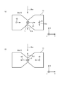
- FIG. 6A and FIG. 6B are diagrams illustrating the principle of the rectifier according to the first embodiment.
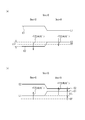
- FIGS. 7A and 7B are schematic diagrams of spin splitting levels depending on the traveling direction of electrons.
- the external magnetic field generation unit 38 generates an external magnetic field Bex in the ⁇ Y direction.
- the drain voltage Vds is positive and the electrons are traveling in the + X direction.
- the effective magnetic field B ⁇ applied to the electrons 40 is in the + Y direction.
- FIG. 7A when the external magnetic field Bex is 0, the level of the electron 40 is spin-separated by the effective magnetic field B ⁇ .
- the spin level E1 spin-polarized in the + Y direction is lower than the spin level E2 spin-polarized in the -Y direction.
- the direction of the external magnetic field Bex is opposite to the direction of the effective magnetic field B ⁇ .
- the energy ⁇ E that increases the spin level E1 by applying the external magnetic field Bex is 1 ⁇ 2 g ⁇ B Bex.
- g is a g factor
- ⁇ B is a magnetic permeability.
- the drain voltage Vds is negative and the electrons are traveling in the ⁇ X direction.
- the effective magnetic field B ⁇ applied to the electrons 40 is in the ⁇ Y direction.
- the external magnetic field Bex when the external magnetic field Bex is 0, the level of the electron 40 is spin-separated by the effective magnetic field B ⁇ .
- the spin level E2 in the ⁇ Y direction is lower than the spin level E1 in the Y direction.
- the energy ⁇ E that lowers the spin level E2 by applying the external magnetic field Bex is 1 ⁇ 2 g ⁇ B Bex.
- the electrons 40 are spin-polarized in the Y direction by the effective magnetic field B ⁇ (see FIG. 6A).
- the energy of the spin level E1 in the + Y direction is increased by the external magnetic field Bex.
- the spin level E1 becomes higher than the Fermi level EF.
- traveling in the X direction of electrons that are spin-polarized in the -Y direction is hindered.
- the electrons 40 are spin-polarized in the ⁇ Y direction by the effective magnetic field B ⁇ (see FIG. 6B). Due to the external magnetic field Bex, the energy of the spin level E2 in the -Y direction is lowered. For example, the spin level E2 is lower than the Fermi level EF.
- the gate electrode 26 applies an electric field to the one-dimensional channel 18, thereby causing the electrons traveling in the one-dimensional channel 18 to travel in an effective magnetic field B ⁇ caused by spin-orbit interaction in the direction in which the electrons travel. Generate in the intersecting direction.
- the external magnetic field generation unit 38 causes the one-dimensional channel 18 to generate an external magnetic field Bex.
- the one-dimensional channel 18 can be formed using a quantum point contact as shown in FIG.
- the external magnetic field Bex generated by the external magnetic field generator 38 is preferably not orthogonal to the effective magnetic field B ⁇ .
- (DELTA) E can be enlarged and a rectification characteristic can be improved more.
- the external magnetic field Bex is preferably generated in the direction of the effective magnetic field B ⁇ as shown in FIG. 7B or in the direction opposite to the effective magnetic field B ⁇ as shown in FIG. Accordingly, ⁇ E in FIGS. 7A and 7B can be maximized, and the rectification characteristics can be further improved.
- the one-dimensional channel 18 preferably has a zinc blende type crystal structure.
- a III-V compound semiconductor is preferable.
- GaAs, InAs, AlAs, GaP, InP, AlP, GaSb, InSb, AlSb, GaN, InN, and AlN can be used as the one-dimensional channel 18.
- these mixed crystals can be used.
- a II-IV group compound semiconductor can also be used as the one-dimensional channel 18.
- the one-dimensional channel 18 When the one-dimensional channel 18 has a zinc blende type crystal structure, it is preferably formed on the (001) plane, the (110) plane, or a plane equivalent to these planes in order to obtain an effective magnetic field B ⁇ .
- the traveling direction of electrons in the one-dimensional channel 18 may be any of in-plane directions.
- the one-dimensional channel 18 is a semiconductor formed in a portion constricted from both sides in the direction in which electrons travel.
- a quantum point contact can be formed by providing a constriction in the semiconductor layer 11 (in particular, the well layer 14).
- side gates 32 for forming a depletion layer are provided on both sides of the constricted portion of the well layer 14.
- the one-dimensional channel 18 can be formed from the depletion layers on both sides of the constricted portion as shown in FIG.
- the rectifier according to the first embodiment can be used for initialization of qubits in quantum computing, for example.
- quantum computing calculations are first performed after the electron spins are aligned in one direction (this is called initialization).
- a qubit is used as one qubit.
- a spin injection source having a size comparable to that of the qubit (for example, several hundred nm).
- spin injection is performed on a semiconductor using a ferromagnetic material, spin injection with a size of several hundred nm has not been realized.
- Example 1 since spin injection can be performed through a one-dimensional channel of about 100 nm, electrons having the same spin direction can be injected into the qubit. Thereby, this rectifier can be used for initialization of qubits in quantum computing, for example.
- the rectifier according to Embodiment 1 can be used for, for example, a spin field effect transistor.
- a spin field effect transistor a ferromagnetic material is used to perform spin injection into a semiconductor. For this reason, a high-quality heterojunction between the ferromagnetic material and the semiconductor is formed. Therefore, an advanced thin film formation technique is required.
- spin polarization can be generated using only a semiconductor. Therefore, this rectifier is a spin polarization source more suitable for a semiconductor device than when a ferromagnetic material is used.
- this rectifier by using the spin rectification effect, it is possible to generate a current with uniform spin using a random energy change, so that it can also be used as a power saving spin polarization source.
- FIG. 8A and FIG. 8B are diagrams for explaining the principle of the transistor according to the second embodiment.
- FIGS. 9A and 9B are schematic diagrams of spin splitting levels depending on the traveling direction of electrons.
- an electric field E in the ⁇ Z direction is applied to the one-dimensional channel by the gate electrode 26.
- the external magnetic field generator 38 generates an external magnetic field Bex in the ⁇ Y direction.
- the drain voltage Vds is positive, and the electrons 40 are traveling in the + X direction.
- the effective magnetic field B ⁇ applied to the electrons 40 is in the ⁇ Y direction.
- the spin level E2 spin-polarized in the ⁇ Y direction is lower than the spin level E2 spin-polarized in the + Y direction.
- the drain voltage Vds is negative and the electrons are traveling in the ⁇ X direction.
- the effective magnetic field B ⁇ applied to the electrons 40 is in the + Y direction.
- the level of the electron 40 is spin-separated by the effective magnetic field B ⁇ .
- the spin level E1 in the + Y direction is lower than the spin level E2 in the -Y direction.
- the source 20 injects electrons into the one-dimensional channel 18 and the drain 22 receives electrons from the one-dimensional channel 18 (that is, when Vds> 0)
- a negative voltage is applied, as shown in FIGS. 6A and 7A, traveling of electrons having spin in the ⁇ Y direction from the source 20 to the drain 22 is suppressed.
- a positive voltage is applied to the gate electrode, as shown in FIGS. 8 (a) and 9 (a)
- the electron 42 travels from the source 20 to the drain 22 in the ⁇ Y direction (arrow 41b). .
- a transistor that turns on or off the flow of electrons spin-polarized in the ⁇ Y direction by the gate voltage can be realized.
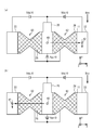
- FIG. 10A and FIG. 10B are schematic plan views for explaining the operation of the third embodiment.
- the crosses in FIG. 10A and FIG. 10B indicate that the gate electrode 26 is formed on the semiconductor layer 11.
- a plurality of transistors 60 and 62 described in the second embodiment are connected.
- the sources 20 of the two transistors 60 and 62 are shared.
- a positive drain voltage Vds is applied between the source 20 and the drain 22. This causes electrons to move in the ⁇ X direction in the transistor 60 and in the X direction in the transistor 62.
- a positive voltage Vgs is applied to the gate electrode 26.
- the transistor 62 electrons that are spin-polarized in the -Y direction flow in the X direction. Therefore, the transistor 60 is cut off. The transistor 62 becomes conductive, and spin-polarized electrons flow from the source 20 to the drain 22.
- a positive drain voltage Vds is applied between the source 20 and the drain 22 and a negative voltage Vgs is applied to the gate electrode 26.
- Vds negative voltage
- Vgs negative voltage
- the transistor 60 electrons that are spin-polarized in the ⁇ Y direction in the ⁇ X direction. 42 flows.
- the transistor 62 the electrons 40 do not flow in the X direction. Thus, the transistor 62 is cut off.
- the transistor 60 becomes conductive, and spin-polarized electrons flow from the source 20 to the drain 22.
- a 1-input 2-output switch circuit can be easily realized.
- various electronic circuits can be realized by using the rectifier of the first embodiment.
- the transistor may have another configuration as long as the transistor includes the rectifier according to the first embodiment.
- the rectifier of Example 1 can also be used for a magnetic sensor or the like.
- the first to third embodiments can be used as electronic parts constituting electronic devices such as home electric devices such as monitors and televisions, communication devices, and computers.
Landscapes
- Engineering & Computer Science (AREA)
- Chemical & Material Sciences (AREA)
- Nanotechnology (AREA)
- Physics & Mathematics (AREA)
- Mathematical Physics (AREA)
- Theoretical Computer Science (AREA)
- Crystallography & Structural Chemistry (AREA)
- Power Engineering (AREA)
- Hall/Mr Elements (AREA)
Abstract
Description
18 一次元チャネル
20 ソース
22 ドレイン
26 ゲート電極
32 サイドゲート
38 外部磁場生成部
60、62 トランジスタ
Claims (10)
- 半導体からなり電子が走行する一次元チャネルと、
前記一次元チャネルに電界を印加することにより、前記一次元チャネルを走行する電子にスピン軌道相互作用に起因する有効磁場を前記電子が走行する方向と交差する方向に生成させる電極と、
前記一次元チャネルに外部磁場を生成する外部磁場生成部と、
を具備することを特徴とする整流装置。 - 前記一次元チャネルは量子ポイントコンタクトであることを特徴とする請求項1記載の整流装置。
- 前記外部磁場生成部は、前記外部磁場を、前記有効磁場の方向または前記有効磁場と反対方向に生成することを特徴とする請求項1記載の整流装置。
- 前記一次元チャネルは、閃亜鉛鉱型結晶構造を有することを特徴とする請求項1から3のいずれか一項記載の整流装置。
- 前記一次元チャネルは、(001)面または(110)面上に形成されていることを特徴とする請求項4記載の整流装置。
- 前記一次元チャネルは、前記電子が走行する方向に対し両側からくびれた箇所に形成される半導体であることを特徴とする請求項1から5のいずれか一項記載の整流装置。
- 前記一次元チャネルの前記くびれた箇所の両側に空乏層を形成するサイドゲートを具備することを特徴とする請求項6記載の整流装置。
- 請求項1から7のいずれか一項記載の整流装置を含むトランジスタ。
- 前記一次元チャネルに電子を注入するソースと、
前記一次元チャネルから電子を受けるドレインと、を具備し、
前記電極はゲート電極であることを特徴とする請求項8記載のトランジスタ。 - 半導体からなり電子が走行している一次元チャネルに、電界を印加することにより、前記一次元チャネルを走行している電子にスピン軌道相互作用に起因する有効磁場を前記電子が走行している方向と交差する方向に生成させるステップと、
前記一次元チャネルに外部磁場を生成するステップと、
を含むことを特徴とする整流方法。
Priority Applications (5)
| Application Number | Priority Date | Filing Date | Title |
|---|---|---|---|
| CN201280039425.2A CN103718303B (zh) | 2011-08-22 | 2012-08-21 | 整流装置、晶体管以及整流方法 |
| JP2013502951A JP5260810B1 (ja) | 2011-08-22 | 2012-08-21 | 整流装置、トランジスタおよび整流方法 |
| EP12825398.6A EP2736080B1 (en) | 2011-08-22 | 2012-08-21 | Spin rectifying device, spin transistor, and spin rectifying method |
| US14/240,219 US9450176B2 (en) | 2011-08-22 | 2012-08-21 | Rectifying device, transistor, and rectifying method |
| KR1020147004002A KR101421075B1 (ko) | 2011-08-22 | 2012-08-21 | 정류 장치, 트랜지스터 및 정류 방법 |
Applications Claiming Priority (2)
| Application Number | Priority Date | Filing Date | Title |
|---|---|---|---|
| JP2011-180767 | 2011-08-22 | ||
| JP2011180767 | 2011-08-22 |
Publications (1)
| Publication Number | Publication Date |
|---|---|
| WO2013027712A1 true WO2013027712A1 (ja) | 2013-02-28 |
Family
ID=47746451
Family Applications (1)
| Application Number | Title | Priority Date | Filing Date |
|---|---|---|---|
| PCT/JP2012/071025 Ceased WO2013027712A1 (ja) | 2011-08-22 | 2012-08-21 | 整流装置、トランジスタおよび整流方法 |
Country Status (6)
| Country | Link |
|---|---|
| US (1) | US9450176B2 (ja) |
| EP (1) | EP2736080B1 (ja) |
| JP (1) | JP5260810B1 (ja) |
| KR (1) | KR101421075B1 (ja) |
| CN (1) | CN103718303B (ja) |
| WO (1) | WO2013027712A1 (ja) |
Cited By (1)
| Publication number | Priority date | Publication date | Assignee | Title |
|---|---|---|---|---|
| JP7658551B2 (ja) | 2020-11-30 | 2025-04-08 | 国立大学法人東北大学 | 電子スピン波の多重伝送方法および電子スピン波の多重伝送装置 |
Families Citing this family (6)
| Publication number | Priority date | Publication date | Assignee | Title |
|---|---|---|---|---|
| US11276756B2 (en) * | 2016-09-30 | 2022-03-15 | Intel Corporation | Quantum dot devices with single electron transistor detectors |
| FR3068518B1 (fr) | 2017-06-28 | 2019-08-30 | Commissariat A L'energie Atomique Et Aux Energies Alternatives | Procede de controle d'un dispositif quantique a qubit de spin |
| WO2019002761A1 (fr) * | 2017-06-28 | 2019-01-03 | Commissariat A L'energie Atomique Et Aux Energies Alternatives | Procede de controle d'un dispositif quantique a qubit de spin |
| CN108100992B (zh) * | 2017-12-20 | 2019-05-28 | 郑州云海信息技术有限公司 | 一种纳米环的量子纠缠态获取方法及其装置 |
| US20240349624A1 (en) * | 2020-10-29 | 2024-10-17 | The Regents Of The University Of California | Spin-orbit rectifier for weak radio frequency energy harvesting |
| CN115775745B (zh) * | 2022-11-14 | 2025-08-08 | 天狼芯半导体(杭州)有限公司 | 一种沟道缺陷检测方法及晶圆检测方法 |
Citations (3)
| Publication number | Priority date | Publication date | Assignee | Title |
|---|---|---|---|---|
| JP2006032570A (ja) * | 2004-07-14 | 2006-02-02 | Nippon Telegr & Teleph Corp <Ntt> | スピンフィルタ及びスピン状態分離方法 |
| JP2011071255A (ja) * | 2009-09-25 | 2011-04-07 | Japan Science & Technology Agency | 電子スピン共鳴生成装置および電子スピン共鳴の生成方法 |
| JP2011082388A (ja) * | 2009-10-08 | 2011-04-21 | Saitama Univ | スピントロニクス装置及び論理演算素子 |
Family Cites Families (22)
| Publication number | Priority date | Publication date | Assignee | Title |
|---|---|---|---|---|
| US4204132A (en) * | 1976-08-11 | 1980-05-20 | Agency Of Industrial Science & Technology, Ministry Of International Trade & Industry | Highly sensitive Hall element |
| JPS5426369U (ja) * | 1977-07-25 | 1979-02-21 | ||
| US4276555A (en) * | 1978-07-13 | 1981-06-30 | International Business Machines Corporation | Controlled avalanche voltage transistor and magnetic sensor |
| US4488164A (en) * | 1982-06-10 | 1984-12-11 | At&T Bell Laboratories | Quantized Hall effect switching devices |
| US5497015A (en) * | 1988-11-12 | 1996-03-05 | Sony Corporation | Quantum interference transistor |
| EP0517647A3 (en) * | 1991-06-04 | 1993-07-21 | Fujitsu Limited | Quantum semiconductor device that uses a quantum point contact for producing a quantum mechanical carrier wave with directivity |
| JP2701633B2 (ja) * | 1991-12-09 | 1998-01-21 | 日本電気株式会社 | 半導体装置 |
| JPH05315598A (ja) * | 1992-05-08 | 1993-11-26 | Fujitsu Ltd | 半導体装置 |
| JP3257034B2 (ja) * | 1992-06-03 | 2002-02-18 | ソニー株式会社 | 化合物半導体装置とその製造方法 |
| JPH06244216A (ja) * | 1992-12-21 | 1994-09-02 | Mitsubishi Electric Corp | Ipgトランジスタ及びその製造方法,並びに半導体集積回路装置及びその製造方法 |
| GB9311111D0 (en) * | 1993-05-28 | 1993-07-14 | Hitachi Europ Ltd | Quantum structure devices |
| JP3621367B2 (ja) * | 2001-09-17 | 2005-02-16 | 株式会社東芝 | スピントランジスタ |
| CN100511748C (zh) * | 2002-01-15 | 2009-07-08 | 旭化成电子材料元件株式会社 | 霍尔元件 |
| KR20050081125A (ko) * | 2004-02-11 | 2005-08-18 | 최중범 | 두 양자비트 양자전산 게이트 |
| US7135697B2 (en) * | 2004-02-25 | 2006-11-14 | Wisconsin Alumni Research Foundation | Spin readout and initialization in semiconductor quantum dots |
| US7492022B2 (en) * | 2004-02-27 | 2009-02-17 | University Of Iowa Research Foundation | Non-magnetic semiconductor spin transistor |
| JP2006066603A (ja) | 2004-08-26 | 2006-03-09 | Nippon Telegr & Teleph Corp <Ntt> | 原子核スピン状態制御装置及び検出装置 |
| KR100619300B1 (ko) * | 2005-09-14 | 2006-09-06 | 한국과학기술연구원 | 스핀-궤도 결합 유도 자장을 이용한 스핀 트랜지스터 |
| EP1830410A1 (en) | 2006-02-24 | 2007-09-05 | Hitachi, Ltd. | Single-charge tunnelling device |
| KR100709395B1 (ko) * | 2006-06-23 | 2007-04-20 | 한국과학기술연구원 | 강자성체를 이용한 스핀 트랜지스터 |
| KR100855105B1 (ko) * | 2007-06-14 | 2008-08-29 | 한국과학기술연구원 | 수직자화를 이용한 스핀 트랜지스터 |
| JP4496242B2 (ja) | 2007-08-29 | 2010-07-07 | 株式会社東芝 | スピントランジスタ及び磁気メモリ |
-
2012
- 2012-08-21 WO PCT/JP2012/071025 patent/WO2013027712A1/ja not_active Ceased
- 2012-08-21 EP EP12825398.6A patent/EP2736080B1/en active Active
- 2012-08-21 KR KR1020147004002A patent/KR101421075B1/ko active Active
- 2012-08-21 JP JP2013502951A patent/JP5260810B1/ja active Active
- 2012-08-21 US US14/240,219 patent/US9450176B2/en active Active
- 2012-08-21 CN CN201280039425.2A patent/CN103718303B/zh active Active
Patent Citations (3)
| Publication number | Priority date | Publication date | Assignee | Title |
|---|---|---|---|---|
| JP2006032570A (ja) * | 2004-07-14 | 2006-02-02 | Nippon Telegr & Teleph Corp <Ntt> | スピンフィルタ及びスピン状態分離方法 |
| JP2011071255A (ja) * | 2009-09-25 | 2011-04-07 | Japan Science & Technology Agency | 電子スピン共鳴生成装置および電子スピン共鳴の生成方法 |
| JP2011082388A (ja) * | 2009-10-08 | 2011-04-21 | Saitama Univ | スピントロニクス装置及び論理演算素子 |
Non-Patent Citations (2)
| Title |
|---|
| APPL. PHYS. LETT., vol. 56, 1990, pages 665 |
| See also references of EP2736080A4 |
Cited By (1)
| Publication number | Priority date | Publication date | Assignee | Title |
|---|---|---|---|---|
| JP7658551B2 (ja) | 2020-11-30 | 2025-04-08 | 国立大学法人東北大学 | 電子スピン波の多重伝送方法および電子スピン波の多重伝送装置 |
Also Published As
| Publication number | Publication date |
|---|---|
| US20140166985A1 (en) | 2014-06-19 |
| EP2736080A1 (en) | 2014-05-28 |
| CN103718303B (zh) | 2015-05-20 |
| EP2736080A4 (en) | 2015-06-24 |
| JPWO2013027712A1 (ja) | 2015-03-19 |
| CN103718303A (zh) | 2014-04-09 |
| KR20140029547A (ko) | 2014-03-10 |
| US9450176B2 (en) | 2016-09-20 |
| JP5260810B1 (ja) | 2013-08-14 |
| EP2736080B1 (en) | 2017-02-01 |
| KR101421075B1 (ko) | 2014-07-18 |
Similar Documents
| Publication | Publication Date | Title |
|---|---|---|
| JP5260810B1 (ja) | 整流装置、トランジスタおよび整流方法 | |
| US7492022B2 (en) | Non-magnetic semiconductor spin transistor | |
| KR100832583B1 (ko) | 누설자장을 이용한 스핀 트랜지스터 | |
| Chen et al. | Electric-field control of interfacial spin–orbit fields | |
| US20150311305A1 (en) | Spin mosfet | |
| Marin et al. | Tunnel-field-effect spin filter from two-dimensional antiferromagnetic stanene | |
| US8058676B2 (en) | Spin transistor using double carrier supply layer structure | |
| Sun et al. | Spin injection, relaxation, and manipulation in GaN-based semiconductors | |
| Ciorga | Perspective on the spin field-effect transistor | |
| Şaşıoğlu et al. | Multifunctional steep-slope spintronic transistors with spin-gapless-semiconductor or spin-gapped-metal electrodes | |
| KR100709395B1 (ko) | 강자성체를 이용한 스핀 트랜지스터 | |
| Ciorga | Electrical spin injection and detection in high mobility 2DEG systems | |
| JP5237232B2 (ja) | 電子スピン共鳴生成装置および電子スピン共鳴の生成方法 | |
| KR101753342B1 (ko) | 상온 작동 스핀제어전자소자 | |
| JP5248446B2 (ja) | 電子回路 | |
| GB2560936A (en) | Spin electronic device | |
| KR101084020B1 (ko) | 이중 전하 공급층 구조를 이용한 스핀 트랜지스터 | |
| Claeys et al. | Challenges for advanced end of the roadmap, beyond Si and beyond CMOS technologies | |
| EP3975275B1 (en) | Insulator-based field effect topological transistor structure | |
| Patel et al. | Investigation of the DC Performance and Linearity of InAlN/GaN HFETs via Studying the Impact of the Scaling of L GS and L G on the Source Access Resistance | |
| Weißhaupt et al. | Lateral Mn5Ge3 spin-valve in contact with a high-mobility Ge two-dimensional hole gas | |
| Böer et al. | Carrier transport in low-dimensional semiconductors | |
| Gupta et al. | 19 Applications of Graphene-Based | |
| Modarresi | The Spin Field-Effect Transistor: Can It Be Realized? | |
| Heedt et al. | Toward spin electronic devices based on semiconductor nanowires |
Legal Events
| Date | Code | Title | Description |
|---|---|---|---|
| ENP | Entry into the national phase |
Ref document number: 2013502951 Country of ref document: JP Kind code of ref document: A |
|
| 121 | Ep: the epo has been informed by wipo that ep was designated in this application |
Ref document number: 12825398 Country of ref document: EP Kind code of ref document: A1 |
|
| ENP | Entry into the national phase |
Ref document number: 20147004002 Country of ref document: KR Kind code of ref document: A |
|
| REEP | Request for entry into the european phase |
Ref document number: 2012825398 Country of ref document: EP |
|
| WWE | Wipo information: entry into national phase |
Ref document number: 14240219 Country of ref document: US Ref document number: 2012825398 Country of ref document: EP |
|
| NENP | Non-entry into the national phase |
Ref country code: DE |